EP2434539A2 - System and method of chip package build-up - Google Patents
System and method of chip package build-up Download PDFInfo
- Publication number
- EP2434539A2 EP2434539A2 EP11174096A EP11174096A EP2434539A2 EP 2434539 A2 EP2434539 A2 EP 2434539A2 EP 11174096 A EP11174096 A EP 11174096A EP 11174096 A EP11174096 A EP 11174096A EP 2434539 A2 EP2434539 A2 EP 2434539A2
- Authority
- EP
- European Patent Office
- Prior art keywords
- die
- adhesive layer
- layer
- base
- chip package
- Prior art date
- Legal status (The legal status is an assumption and is not a legal conclusion. Google has not performed a legal analysis and makes no representation as to the accuracy of the status listed.)
- Granted
Links
Images


Classifications
-
- H—ELECTRICITY
- H10—SEMICONDUCTOR DEVICES; ELECTRIC SOLID-STATE DEVICES NOT OTHERWISE PROVIDED FOR
- H10W—GENERIC PACKAGES, INTERCONNECTIONS, CONNECTORS OR OTHER CONSTRUCTIONAL DETAILS OF DEVICES COVERED BY CLASS H10
- H10W42/00—Arrangements for protection of devices
- H10W42/121—Arrangements for protection of devices protecting against mechanical damage
-
- H—ELECTRICITY
- H10—SEMICONDUCTOR DEVICES; ELECTRIC SOLID-STATE DEVICES NOT OTHERWISE PROVIDED FOR
- H10W—GENERIC PACKAGES, INTERCONNECTIONS, CONNECTORS OR OTHER CONSTRUCTIONAL DETAILS OF DEVICES COVERED BY CLASS H10
- H10W72/00—Interconnections or connectors in packages
-
- H—ELECTRICITY
- H10—SEMICONDUCTOR DEVICES; ELECTRIC SOLID-STATE DEVICES NOT OTHERWISE PROVIDED FOR
- H10W—GENERIC PACKAGES, INTERCONNECTIONS, CONNECTORS OR OTHER CONSTRUCTIONAL DETAILS OF DEVICES COVERED BY CLASS H10
- H10W72/00—Interconnections or connectors in packages
- H10W72/01—Manufacture or treatment
- H10W72/013—Manufacture or treatment of die-attach connectors
-
- H—ELECTRICITY
- H10—SEMICONDUCTOR DEVICES; ELECTRIC SOLID-STATE DEVICES NOT OTHERWISE PROVIDED FOR
- H10W—GENERIC PACKAGES, INTERCONNECTIONS, CONNECTORS OR OTHER CONSTRUCTIONAL DETAILS OF DEVICES COVERED BY CLASS H10
- H10W20/00—Interconnections in chips, wafers or substrates
- H10W20/20—Interconnections within wafers or substrates, e.g. through-silicon vias [TSV]
-
- H—ELECTRICITY
- H10—SEMICONDUCTOR DEVICES; ELECTRIC SOLID-STATE DEVICES NOT OTHERWISE PROVIDED FOR
- H10W—GENERIC PACKAGES, INTERCONNECTIONS, CONNECTORS OR OTHER CONSTRUCTIONAL DETAILS OF DEVICES COVERED BY CLASS H10
- H10W20/00—Interconnections in chips, wafers or substrates
- H10W20/40—Interconnections external to wafers or substrates, e.g. back-end-of-line [BEOL] metallisations or vias connecting to gate electrodes
- H10W20/41—Interconnections external to wafers or substrates, e.g. back-end-of-line [BEOL] metallisations or vias connecting to gate electrodes characterised by their conductive parts
- H10W20/42—Vias, e.g. via plugs
-
- H—ELECTRICITY
- H10—SEMICONDUCTOR DEVICES; ELECTRIC SOLID-STATE DEVICES NOT OTHERWISE PROVIDED FOR
- H10W—GENERIC PACKAGES, INTERCONNECTIONS, CONNECTORS OR OTHER CONSTRUCTIONAL DETAILS OF DEVICES COVERED BY CLASS H10
- H10W70/00—Package substrates; Interposers; Redistribution layers [RDL]
- H10W70/01—Manufacture or treatment
- H10W70/05—Manufacture or treatment of insulating or insulated package substrates, or of interposers, or of redistribution layers
- H10W70/08—Manufacture or treatment of insulating or insulated package substrates, or of interposers, or of redistribution layers by depositing layers on the chip or wafer, e.g. "chip-first" RDLs
- H10W70/09—Manufacture or treatment of insulating or insulated package substrates, or of interposers, or of redistribution layers by depositing layers on the chip or wafer, e.g. "chip-first" RDLs extending onto an encapsulation that laterally surrounds the chip or wafer, e.g. fan-out wafer level package [FOWLP] RDLs
-
- H—ELECTRICITY
- H10—SEMICONDUCTOR DEVICES; ELECTRIC SOLID-STATE DEVICES NOT OTHERWISE PROVIDED FOR
- H10W—GENERIC PACKAGES, INTERCONNECTIONS, CONNECTORS OR OTHER CONSTRUCTIONAL DETAILS OF DEVICES COVERED BY CLASS H10
- H10W70/00—Package substrates; Interposers; Redistribution layers [RDL]
- H10W70/60—Insulating or insulated package substrates; Interposers; Redistribution layers
-
- H—ELECTRICITY
- H10—SEMICONDUCTOR DEVICES; ELECTRIC SOLID-STATE DEVICES NOT OTHERWISE PROVIDED FOR
- H10W—GENERIC PACKAGES, INTERCONNECTIONS, CONNECTORS OR OTHER CONSTRUCTIONAL DETAILS OF DEVICES COVERED BY CLASS H10
- H10W72/00—Interconnections or connectors in packages
- H10W72/30—Die-attach connectors
-
- H—ELECTRICITY
- H10—SEMICONDUCTOR DEVICES; ELECTRIC SOLID-STATE DEVICES NOT OTHERWISE PROVIDED FOR
- H10W—GENERIC PACKAGES, INTERCONNECTIONS, CONNECTORS OR OTHER CONSTRUCTIONAL DETAILS OF DEVICES COVERED BY CLASS H10
- H10W70/00—Package substrates; Interposers; Redistribution layers [RDL]
- H10W70/01—Manufacture or treatment
- H10W70/05—Manufacture or treatment of insulating or insulated package substrates, or of interposers, or of redistribution layers
- H10W70/093—Connecting or disconnecting other interconnections thereto or therefrom, e.g. connecting bond wires or bumps
-
- H—ELECTRICITY
- H10—SEMICONDUCTOR DEVICES; ELECTRIC SOLID-STATE DEVICES NOT OTHERWISE PROVIDED FOR
- H10W—GENERIC PACKAGES, INTERCONNECTIONS, CONNECTORS OR OTHER CONSTRUCTIONAL DETAILS OF DEVICES COVERED BY CLASS H10
- H10W70/00—Package substrates; Interposers; Redistribution layers [RDL]
- H10W70/60—Insulating or insulated package substrates; Interposers; Redistribution layers
- H10W70/67—Insulating or insulated package substrates; Interposers; Redistribution layers characterised by their insulating layers or insulating parts
- H10W70/68—Shapes or dispositions thereof
- H10W70/681—Shapes or dispositions thereof comprising holes not having chips therein, e.g. for outgassing, underfilling or bond wire passage
-
- H—ELECTRICITY
- H10—SEMICONDUCTOR DEVICES; ELECTRIC SOLID-STATE DEVICES NOT OTHERWISE PROVIDED FOR
- H10W—GENERIC PACKAGES, INTERCONNECTIONS, CONNECTORS OR OTHER CONSTRUCTIONAL DETAILS OF DEVICES COVERED BY CLASS H10
- H10W72/00—Interconnections or connectors in packages
- H10W72/01—Manufacture or treatment
- H10W72/0198—Manufacture or treatment batch processes
-
- H—ELECTRICITY
- H10—SEMICONDUCTOR DEVICES; ELECTRIC SOLID-STATE DEVICES NOT OTHERWISE PROVIDED FOR
- H10W—GENERIC PACKAGES, INTERCONNECTIONS, CONNECTORS OR OTHER CONSTRUCTIONAL DETAILS OF DEVICES COVERED BY CLASS H10
- H10W72/00—Interconnections or connectors in packages
- H10W72/071—Connecting or disconnecting
- H10W72/073—Connecting or disconnecting of die-attach connectors
-
- H—ELECTRICITY
- H10—SEMICONDUCTOR DEVICES; ELECTRIC SOLID-STATE DEVICES NOT OTHERWISE PROVIDED FOR
- H10W—GENERIC PACKAGES, INTERCONNECTIONS, CONNECTORS OR OTHER CONSTRUCTIONAL DETAILS OF DEVICES COVERED BY CLASS H10
- H10W72/00—Interconnections or connectors in packages
- H10W72/071—Connecting or disconnecting
- H10W72/073—Connecting or disconnecting of die-attach connectors
- H10W72/07331—Connecting techniques
- H10W72/07337—Connecting techniques using a polymer adhesive, e.g. an adhesive based on silicone or epoxy
- H10W72/07338—Connecting techniques using a polymer adhesive, e.g. an adhesive based on silicone or epoxy hardening the adhesive by curing, e.g. thermosetting
-
- H—ELECTRICITY
- H10—SEMICONDUCTOR DEVICES; ELECTRIC SOLID-STATE DEVICES NOT OTHERWISE PROVIDED FOR
- H10W—GENERIC PACKAGES, INTERCONNECTIONS, CONNECTORS OR OTHER CONSTRUCTIONAL DETAILS OF DEVICES COVERED BY CLASS H10
- H10W72/00—Interconnections or connectors in packages
- H10W72/30—Die-attach connectors
- H10W72/351—Materials of die-attach connectors
- H10W72/352—Materials of die-attach connectors comprising metals or metalloids, e.g. solders
-
- H—ELECTRICITY
- H10—SEMICONDUCTOR DEVICES; ELECTRIC SOLID-STATE DEVICES NOT OTHERWISE PROVIDED FOR
- H10W—GENERIC PACKAGES, INTERCONNECTIONS, CONNECTORS OR OTHER CONSTRUCTIONAL DETAILS OF DEVICES COVERED BY CLASS H10
- H10W72/00—Interconnections or connectors in packages
- H10W72/30—Die-attach connectors
- H10W72/351—Materials of die-attach connectors
- H10W72/353—Materials of die-attach connectors not comprising solid metals or solid metalloids, e.g. ceramics
- H10W72/354—Materials of die-attach connectors not comprising solid metals or solid metalloids, e.g. ceramics comprising polymers
-
- H—ELECTRICITY
- H10—SEMICONDUCTOR DEVICES; ELECTRIC SOLID-STATE DEVICES NOT OTHERWISE PROVIDED FOR
- H10W—GENERIC PACKAGES, INTERCONNECTIONS, CONNECTORS OR OTHER CONSTRUCTIONAL DETAILS OF DEVICES COVERED BY CLASS H10
- H10W72/00—Interconnections or connectors in packages
- H10W72/90—Bond pads, in general
- H10W72/941—Dispositions of bond pads
- H10W72/9413—Dispositions of bond pads on encapsulations
-
- H—ELECTRICITY
- H10—SEMICONDUCTOR DEVICES; ELECTRIC SOLID-STATE DEVICES NOT OTHERWISE PROVIDED FOR
- H10W—GENERIC PACKAGES, INTERCONNECTIONS, CONNECTORS OR OTHER CONSTRUCTIONAL DETAILS OF DEVICES COVERED BY CLASS H10
- H10W76/00—Containers; Fillings or auxiliary members therefor; Seals
- H10W76/10—Containers or parts thereof
- H10W76/12—Containers or parts thereof characterised by their shape
- H10W76/167—Containers or parts thereof characterised by their shape the container walls comprising an aperture, e.g. for pressure control
-
- H—ELECTRICITY
- H10—SEMICONDUCTOR DEVICES; ELECTRIC SOLID-STATE DEVICES NOT OTHERWISE PROVIDED FOR
- H10W—GENERIC PACKAGES, INTERCONNECTIONS, CONNECTORS OR OTHER CONSTRUCTIONAL DETAILS OF DEVICES COVERED BY CLASS H10
- H10W99/00—Subject matter not provided for in other groups of this subclass
Definitions
- Embodiments of the invention relate generally to integrated circuit chip packages and, more particularly, to chip package build-up. Chip packages are manufactured using a technique that protects the die from contamination during a build-up process of the chip package.
- Integrated circuit (IC) chip packages are typically fabricated to include one or more dies that are attached to a laminate re-distribution layer.
- the laminate re-distribution layer is comprised of a dielectric laminate material, such as Kapton®, and is affixed to the die by way of an adhesive layer.
- the die(s) are electrically connected to an input/output system by way of metal interconnects routed through a plurality of additional laminate re-distribution layers that are adhered to the base re-distribution layer.
- a standard chip package manufacturing or build-up process typically begins with providing of the base laminate re-distribution layer and application of an adhesive on one surface thereof.
- the one or more dies are then secured relative to the base laminate re-distribution layer by applying a front or active face of the die(s) onto the adhesive layer such that a bond is formed between the active face of the die(s) and the adhesive layer across the full face of the die(s).
- Metal interconnects are then formed and routed through the base laminate re-distribution layer and through any additional laminate re-distribution layers that are subsequently added during build-up of the chip package.
- Deposition of the die(s) onto the base re-distribution layer in this manner has inherent limitations in regards to the production process and the structure and functionality of the resulting chip package that is produced. That is, in some applications it is desirable that the active face of the die(s) be protected from possible contamination during the build-up process of the chip package. For example, for application of the chip package in an imaging device such as an ultra camera or similar sensing device, it is desired that the imager area (i.e., the die) be protected from contamination during the build-up process.
- Various embodiments of the invention address the aforementioned drawbacks by providing a method of chip fabrication in which the chip package is manufactured using a removable shield element that is placed over the die and separated therefrom by an air pocket.
- the shield element protects the die from contamination during the build-up process and can be subsequently removed therefrom to expose a clean front surface of the die.
- a chip package in accordance with one aspect of the invention, includes a base re-distribution layer having an opening formed therein in a center area of the base re-distribution layer, an adhesive layer applied to one side of the base re-distribution layer having a window formed therein free of adhesive material, and a die having a front surface affixed to the base re-distribution layer by way of the adhesive layer, wherein the die is aligned with the window formed in the adhesive layer such that only a perimeter of the front surface of the die is in contact with the adhesive layer.
- the chip package also includes a plurality of vias and a plurality of metal interconnects formed in the base re-distribution layer to electrically connect the base re-distribution layer to the die and a shield element positioned between the base re-distribution layer and the adhesive layer and generally aligned with the opening formed in the base re-distribution layer and the window of the adhesive layer such that only a perimeter of the shield element is attached to the adhesive layer, with the shield element being separated from the die by an air gap.
- the shield element is configured to be selectively removable from the adhesive layer so as to expose the front surface of the die.
- a method of forming a chip package includes providing an initial polymer laminate layer, depositing a metallic shield element on one surface of the initial polymer laminate layer so as to cover a portion thereof, and applying an adhesive layer to the initial polymer laminate layer and over the metallic shield element, the adhesive layer having a portion removed therefrom to form a window in the adhesive layer that corresponds substantially to a surface area of the metallic shield element and aligned therewith.
- the method also includes adhering a die to the initial polymer laminate layer by way of the adhesive layer, with the die being positioned over the window such a perimeter of the die is in contact with the adhesive layer and an air pocket is formed between a center portion of the die and the shield element.
- the method further includes patterning the initial polymer laminate layer to include a plurality of vias and a plurality of metal interconnects so as to electrically connect the initial polymer laminate layer to the die, defining a portion of the initial polymer laminate layer corresponding to the window in the adhesive layer, and removing the portion of the initial polymer laminate layer and the metallic shield element from the adhesive layer so as to expose a front surface of the die.
- a method for manufacturing a chip module includes providing a base re-distribution layer, depositing a shield element on one surface of the base re-distribution layer so as to cover a portion thereof, applying an adhesive layer to the base re-distribution layer and over the shield element, ablating a portion of the adhesive layer in an area adjacent to the shield element so as to expose at least a majority of the shield element, and applying a front surface of a die to the adhesive layer such that the die is aligned with the shield element, wherein a perimeter of the die is in contact with the adhesive layer and a center portion of the die is separated from the shield element by an air gap formed therebetween.
- the method also includes maintaining the shield element in place during a subsequent patterning of the base re-distribution layer that forms a plurality of vias and a plurality of metal interconnects to electrically connect the base re-distribution layer to the die, ablating a portion of the base re-distribution layer adjacent to the shield element, and removing the shield element and the portion of the base distribution layer so as to expose the front surface of the die.
- Various embodiments of the present invention provide for a method of forming a chip package.
- the chip package is manufactured using a shield element or protective layer to protect the surface of a die during build-up and patterning of laminate re-distribution layers of the chip package.
- Each chip package 10 includes a die 12 connected with a plurality of re-distribution layers 14 (i.e., laminate layers).
- Each die 12 is formed from a monosilicon crystal ingot or polysilicon crystal ingot and prepared such that an integrated circuit (IC) layout is formed on its surface.
- IC integrated circuit
- die 12 is configured for use in an imaging device such as an ultra camera, cellular phone camera, or similar sensing device. Die 12 is thus constructed as a "camera die” that forms an imaging area for image sensing.
- each of the plurality of re-distribution layers 14 is in the form of a pre-formed laminate sheet or film that can be placed relative to the die 12.
- the re-distribution layers 14 can be formed of Kapton®, Ultem®, polytetrafluoroethylene (PTFE), or another polymer film, such as a liquid crystal polymer (LCP) or a polyimide material.
- PTFE polytetrafluoroethylene
- LCP liquid crystal polymer
- polyimide material such as a liquid crystal polymer (LCP) or a polyimide material.
- each chip package 10 is formed by dicing through re-distribution layers 14 in an area between adjacent chip packages 10.
- steps in a technique for manufacturing a plurality of chip packages 10 are set forth, according to an embodiment of the invention, with side cross-sectional views and top views of chip package(s) 10 being shown at various stages of the build-up process.
- a complete frame of an initial or base re-distribution layer 16 is provided and mounted on a frame 18 to allow for additional manufacturing steps to be performed thereon.
- the initial re-distribution layer 16 is in the form of a flexible polymer laminate layer, such as Kapton®, Ultem®, polytetrafluoroethylene (PTFE), or another polymer/polyimide film, and is of a size that allows for the production of a plurality of chip packages 10 therefrom.
- a flexible polymer laminate layer such as Kapton®, Ultem®, polytetrafluoroethylene (PTFE), or another polymer/polyimide film
- FIGS. 3-9 A portion of the complete frame of the initial re-distribution layer 16, and of additional layers and components added thereto, is shown in FIGS. 3-9 , such that build-up of a single chip package 10 is illustrated.
- initial re-distribution layer 16 is provided.
- a metal layer 18 is then deposited on one side of initial re-distribution layer 16, as shown in FIGS. 4A and 4B , with the metal layer 18 being formed of a material that will provide a suitable bond with an adhesive that will subsequently be applied (e.g., Ti/Cu/Ti, chrome, etc.).
- the metal layer 18 may be sputtered on initial re-distribution layer 16 or added in any other suitable manner, such as electroplating.
- the metal layer 18 is patterned such that a protective shield element 20 is formed having an area that, according to one embodiment, substantially matches an area of die 12 ( FIG. 1 ) to be subsequently added to chip package 10, as will be explained in detail below. Alternatively, it is recognized that protective shield element 20 could be formed to have an area much smaller than an area of a die 12 ( FIG. 1 ).
- metal layer 18 is further patterned to form a vent base 21 that extends out from shield element 20 past an area of die 12 ( FIG. 1 ) to be added.
- metal layer 18 may be further patterned so as to form a plurality of base metal interconnects 22 on initial re-distribution layer 16.
- an adhesive layer 24 is applied to initial re-distribution layer 16 and over metal layer 18.
- the adhesive layer 24 may be applied to initial re-distribution layer 16 via a spin coating application of an ablatable epoxy or may alternatively be in the form of an adhesive film that is applied onto initial re-distribution layer 16.
- the adhesive layer 24 is then partially cured or baked. Upon partial curing, the adhesive layer 24 is ablated, such as by way of an ultraviolet (UV) laser, so as to form a window 26 as shown in FIGS. 6A and 6B .
- UV ultraviolet
- the adhesive layer 24 that was applied over shield element 20 is laser ablated so as to form a window 26 that exposes the shield element 20.
- the adhesive layer 24 that was applied over vent base 21 is laser ablated so as to also form a small vent 28 to the outside of the die area (i.e., extending out from window 26).
- shield element 20 and vent base 21 act as a "back stop" that prevents the laser from passing therethrough to the initial re-distribution layer 16.
- a pre-cut laminate film could be applied to initial re-distribution layer 16. That is, rather than applying a continuous adhesive layer 24 via spin coating and subsequently laser ablating the adhesive layer 24 to form window 26, as shown in FIGS. 5 and 6A/6B , an adhesive film with a window pre-formed therein could be applied to initial re-distribution layer 16, such that no laser ablating of the adhesive layer is required.
- a portion 30 of the adhesive layer 24 surrounding the ablated area i.e., window 26
- UV light This exposure to UV light partially cures portion 30 such that the adhesive layer 24 is prevented from encroaching into the ablated window 26.
- the build-up of chip package 10 continues with the aligning and placing of die 12 (i.e., IC) onto initial re-distribution layer 16 by way of adhesive layer 24.
- the die 12 is centered over window 26 and is pressed onto adhesive layer 24, at which time the adhesive layer 24 is fully cured so as to secure the die 12 to initial re-distribution layer 16, such as by way of a vacuum lamination and pressure bake curing process.
- the die 12 is sized such that it extends out past shield element 20.
- die pads 32 formed around a periphery of the die 12 thus are positioned outside the area of die 12 covered by shield element 20, allowing for subsequent electrical connection to the die pads 32. Additionally, as die 12 extends out past shield element 20, the die 12 thus rests on adhesive layer 24 and forms an air pocket 36 between the die 12 and shield element 20.
- the air gap 36 in conjunction with shield element 20, functions to keep a top surface of die 12 clean of contamination.
- a vent port 28 is ablated into adhesive layer 24, with the vent port 28 extending outward from air pocket 36 to a region of chip package 10 outside of that covered by die 12. As the vent port 28 provides fluid communication between air gap 36 and an ambient environment outside an area covered by die 12, pressure in the air gap 36 can thus be controlled, such as pressure that might otherwise increase in air pocket 36 during temperature cycling associated with the build-up process of chip package 10.
- the initial re-distribution layer 16 is patterned to have a plurality of vias 38 which are drilled through the polymer material forming the re-distribution layer 16.
- the vias 38 are formed by way of a laser ablation or laser drilling process and are formed at positions corresponding to base metal interconnects 22 and to die pads 32, so as to expose the base metal interconnects 22 and die pads 32.
- vias 38 may be formed by way of other methods including: plasma etching, photo-defmition, or mechanical drilling processes.
- the patterning of the initial re-distribution layer 16 includes the application of a metal layer/material (e.g., a seed metal and/or copper) applied onto the re-distribution layer 16 by way of, for example, a sputtering or electroplating process and the subsequent patterning/etching of the deposited metal layer/material to form metal interconnects 40.
- the metal layer/material is patterned and etched such that metal interconnects 40 are formed that extend from a top surface of initial re-distribution layer 16 and down through vias 38. Metal interconnects 40 thus form an electrical connection with base metal interconnects 22 and die pads 32.
- one or more additional re-distribution layers 42 are laminated onto the initial re-distribution layer 16 on a side of chip package 10 opposite from which the die 12 was applied.
- the additional re-distribution layer(s) 42 are applied to the initial re-distribution layer 16 through a series of lamination and patterning steps.
- An adhesive layer 44 is applied between the initial re-distribution layer 16 and an additional re-distribution layer 42 applied thereto.
- a plurality of vias 38 is formed in the additional re-distribution layer(s) 42, and metal interconnects 40 are formed/patterned to extend down through vias 38 and through the additional re-distribution layer(s) 42, so as to electrically connect each additional re-distribution layer 42. While only one additional re-distribution layer 42 is shown applied to initial re-distribution layer 16 to form chip package 10, it is recognized that more re-distribution layers could be applied based on a desired configuration. As shown in FIG. 9 , in further steps of the build-up process, a solder mask 46 can be applied to an outermost additional re-distribution layer 42 and subsequently patterned so as to provide protection thereto. It is also envisioned that additional components, such as passive devices (not shown), may also be added to chip package 10, with the passive attach being performed while protective shield 20 is in place, such that die 12 is protected during such a passive attach.
- passive devices may also be added to chip package 10, with the passive
- the initial re-distribution layer 16, additional re-distribution layer(s) 42, and adhesive layer(s) 44 are laser ablated along a path 48 corresponding to a perimeter of protective shield 20, so as to define or separate out a portion 50 of the initial re-distribution layer 16, additional re-distribution layer(s) 42, and adhesive layer(s) 44.
- the laser ablation is performed through the initial re-distribution layer 16, additional re-distribution layer(s) 42, and adhesive layer(s) 44 down to protective shield 20, where the laser is stopped by the protective shield 20.
- portion 50 of the initial re-distribution layer 16, additional re-distribution layer(s) 42, and adhesive layer(s) 44 positioned above protective shield 20, about which the laser ablation was performed, is removed from chip package 10 along with protective shield 20. That is, protective shield 20 sticks to initial re-distribution layer 16 and tears readily from adhesive layer 24, such that it can be removed from chip package 10 along with portion 50 in a single removal step. According to embodiments of the invention, portion 50 and protective shield 20 can be removed via one of several techniques, such as vacuum pickup or water scrubbing.
- portion 50 and protective shield 20 exposes the front surface 52 of die 12 (i.e., die front) in the completed chip package 10.
- the die front 52 should be clean of contamination.
- chip package 10 provides for a chip package build-up that protects die 12 from contamination during the build-up process. Additionally, the build-up technique provides for manufacturing of a chip package 10 having a decreased thickness, limited only be minimum thickness requirements of die 12 and re-distribution layer(s) 16, 42.
- a reduced thickness chip package 10 may be configured for use in an imaging device such as an ultra camera, cellular phone camera, or similar sensing device, with the build-up process allowing for mounting of a camera lens (not shown) directly to chip package 10.
- the reduced thickness chip package 10 could be configured for use in other device types, such as microwave devices, or other devices that would benefit from the manufacturing technique set forth above.
- a chip package includes a base re-distribution layer having an opening formed therein in a center area of the base re-distribution layer, an adhesive layer applied to one side of the base re-distribution layer having a window formed therein free of adhesive material, and a die having a front surface affixed to the base re-distribution layer by way of the adhesive layer, wherein the die is aligned with the window formed in the adhesive layer such that only a perimeter of the front surface of the die is in contact with the adhesive layer.
- the chip package also includes a plurality of vias and a plurality of metal interconnects formed in the base re-distribution layer to electrically connect the base re-distribution layer to the die and a shield element positioned between the base re-distribution layer and the adhesive layer and generally aligned with the opening formed in the base re-distribution layer and the window of the adhesive layer such that only a perimeter of the shield element is attached to the adhesive layer, with the shield element being separated from the die by an air gap.
- the shield element is configured to be selectively removable from the adhesive layer so as to expose the front surface of the die.
- a method of forming a chip package includes providing an initial polymer laminate layer, depositing a metallic shield element on one surface of the initial polymer laminate layer so as to cover a portion thereof, and applying an adhesive layer to the initial polymer laminate layer and over the metallic shield element, the adhesive layer having a portion removed therefrom to form a window in the adhesive layer that corresponds substantially to a surface area of the metallic shield element and aligned therewith.
- the method also includes adhering a die to the initial polymer laminate layer by way of the adhesive layer, with the die being positioned over the window such a perimeter of the die is in contact with the adhesive layer and an air pocket is formed between a center portion of the die and the shield element.
- the method further includes patterning the initial polymer laminate layer to include a plurality of vias and a plurality of metal interconnects so as to electrically connect the initial polymer laminate layer to the die, defining a portion of the initial polymer laminate layer corresponding to the window in the adhesive layer, and removing the portion of the initial polymer laminate layer and the metallic shield element from the adhesive layer so as to expose a front surface of the die.
- a method for manufacturing a chip module includes providing a base re-distribution layer, depositing a shield element on one surface of the base re-distribution layer so as to cover a portion thereof, applying an adhesive layer to the base re-distribution layer and over the shield element, ablating a portion of the adhesive layer in an area adjacent to the shield element so as to expose at least a majority of the shield element, and applying a front surface of a die to the adhesive layer such that the die is aligned with the shield element, wherein a perimeter of the die is in contact with the adhesive layer and a center portion of the die is separated from the shield element by an air gap formed therebetween.
- the method also includes maintaining the shield element in place during a subsequent patterning of the base re-distribution layer that forms a plurality of vias and a plurality of metal interconnects to electrically connect the base re-distribution layer to the die, ablating a portion of the base re-distribution layer adjacent to the shield element, and removing the shield element and the portion of the base distribution layer so as to expose the front surface of the die.
Landscapes
- Encapsulation Of And Coatings For Semiconductor Or Solid State Devices (AREA)
- Production Of Multi-Layered Print Wiring Board (AREA)
- Shielding Devices Or Components To Electric Or Magnetic Fields (AREA)
- Die Bonding (AREA)
- Solid State Image Pick-Up Elements (AREA)
- Structures Or Materials For Encapsulating Or Coating Semiconductor Devices Or Solid State Devices (AREA)
Abstract
Description
- Embodiments of the invention relate generally to integrated circuit chip packages and, more particularly, to chip package build-up. Chip packages are manufactured using a technique that protects the die from contamination during a build-up process of the chip package.
- Integrated circuit (IC) chip packages are typically fabricated to include one or more dies that are attached to a laminate re-distribution layer. The laminate re-distribution layer is comprised of a dielectric laminate material, such as Kapton®, and is affixed to the die by way of an adhesive layer. The die(s) are electrically connected to an input/output system by way of metal interconnects routed through a plurality of additional laminate re-distribution layers that are adhered to the base re-distribution layer.
- A standard chip package manufacturing or build-up process typically begins with providing of the base laminate re-distribution layer and application of an adhesive on one surface thereof. The one or more dies are then secured relative to the base laminate re-distribution layer by applying a front or active face of the die(s) onto the adhesive layer such that a bond is formed between the active face of the die(s) and the adhesive layer across the full face of the die(s). Metal interconnects are then formed and routed through the base laminate re-distribution layer and through any additional laminate re-distribution layers that are subsequently added during build-up of the chip package.
- Deposition of the die(s) onto the base re-distribution layer in this manner, however, has inherent limitations in regards to the production process and the structure and functionality of the resulting chip package that is produced. That is, in some applications it is desirable that the active face of the die(s) be protected from possible contamination during the build-up process of the chip package. For example, for application of the chip package in an imaging device such as an ultra camera or similar sensing device, it is desired that the imager area (i.e., the die) be protected from contamination during the build-up process. As the imager area/die in such an application is to be left exposed upon completion of the build-up of the chip package, it is undesirable for a bond to be formed between the active face of the die and the adhesive layer across the full face of the die during the build-up process. Such a build-up would require subsequent removal of the adhesive from the imaging area and could introduce contaminates to the imaging area, thereby negatively affecting the performance of the ultra camera/sensing device.
- Accordingly there is a need for a method for chip package fabrication that protects the die from contamination during the build-up process. There is a further need for the fabrication method to be readily incorporated into an assembly process, be compatible with laser drilling, be scalable, and provide for a low cost assembly.
- Various embodiments of the invention address the aforementioned drawbacks by providing a method of chip fabrication in which the chip package is manufactured using a removable shield element that is placed over the die and separated therefrom by an air pocket. The shield element protects the die from contamination during the build-up process and can be subsequently removed therefrom to expose a clean front surface of the die.
- In accordance with one aspect of the invention, a chip package includes a base re-distribution layer having an opening formed therein in a center area of the base re-distribution layer, an adhesive layer applied to one side of the base re-distribution layer having a window formed therein free of adhesive material, and a die having a front surface affixed to the base re-distribution layer by way of the adhesive layer, wherein the die is aligned with the window formed in the adhesive layer such that only a perimeter of the front surface of the die is in contact with the adhesive layer. The chip package also includes a plurality of vias and a plurality of metal interconnects formed in the base re-distribution layer to electrically connect the base re-distribution layer to the die and a shield element positioned between the base re-distribution layer and the adhesive layer and generally aligned with the opening formed in the base re-distribution layer and the window of the adhesive layer such that only a perimeter of the shield element is attached to the adhesive layer, with the shield element being separated from the die by an air gap. The shield element is configured to be selectively removable from the adhesive layer so as to expose the front surface of the die.
- In accordance with another aspect of the invention, a method of forming a chip package includes providing an initial polymer laminate layer, depositing a metallic shield element on one surface of the initial polymer laminate layer so as to cover a portion thereof, and applying an adhesive layer to the initial polymer laminate layer and over the metallic shield element, the adhesive layer having a portion removed therefrom to form a window in the adhesive layer that corresponds substantially to a surface area of the metallic shield element and aligned therewith. The method also includes adhering a die to the initial polymer laminate layer by way of the adhesive layer, with the die being positioned over the window such a perimeter of the die is in contact with the adhesive layer and an air pocket is formed between a center portion of the die and the shield element. The method further includes patterning the initial polymer laminate layer to include a plurality of vias and a plurality of metal interconnects so as to electrically connect the initial polymer laminate layer to the die, defining a portion of the initial polymer laminate layer corresponding to the window in the adhesive layer, and removing the portion of the initial polymer laminate layer and the metallic shield element from the adhesive layer so as to expose a front surface of the die.
- In accordance with yet another aspect of the invention, a method for manufacturing a chip module includes providing a base re-distribution layer, depositing a shield element on one surface of the base re-distribution layer so as to cover a portion thereof, applying an adhesive layer to the base re-distribution layer and over the shield element, ablating a portion of the adhesive layer in an area adjacent to the shield element so as to expose at least a majority of the shield element, and applying a front surface of a die to the adhesive layer such that the die is aligned with the shield element, wherein a perimeter of the die is in contact with the adhesive layer and a center portion of the die is separated from the shield element by an air gap formed therebetween. The method also includes maintaining the shield element in place during a subsequent patterning of the base re-distribution layer that forms a plurality of vias and a plurality of metal interconnects to electrically connect the base re-distribution layer to the die, ablating a portion of the base re-distribution layer adjacent to the shield element, and removing the shield element and the portion of the base distribution layer so as to expose the front surface of the die.
- Various advantages and features will be more readily understood from the following detailed description of preferred embodiments of the invention that is provided in connection with the accompanying drawings, in which:
-
FIG. 1 is a top view of a plurality of embedded chip packages according to an embodiment of the invention. -
FIGS. 2-11 are cross-sectional side views and top views of an embedded chip package during various stages of a manufacturing/build-up process according to an embodiment of the invention. - Various embodiments of the present invention provide for a method of forming a chip package. The chip package is manufactured using a shield element or protective layer to protect the surface of a die during build-up and patterning of laminate re-distribution layers of the chip package.
- Referring to
FIG. 1 , a plurality of manufacturedchip packages 10 or chip modules are shown. Eachchip package 10 includes a die 12 connected with a plurality of re-distribution layers 14 (i.e., laminate layers). Each die 12 is formed from a monosilicon crystal ingot or polysilicon crystal ingot and prepared such that an integrated circuit (IC) layout is formed on its surface. According to one embodiment of the invention, die 12 is configured for use in an imaging device such as an ultra camera, cellular phone camera, or similar sensing device. Die 12 is thus constructed as a "camera die" that forms an imaging area for image sensing. Regardingre-distribution layers 14 ofchip package 10, each of the plurality ofre-distribution layers 14 is in the form of a pre-formed laminate sheet or film that can be placed relative to the die 12. There-distribution layers 14 can be formed of Kapton®, Ultem®, polytetrafluoroethylene (PTFE), or another polymer film, such as a liquid crystal polymer (LCP) or a polyimide material. As shown inFIG. 1 , eachchip package 10 is formed by dicing throughre-distribution layers 14 in an area betweenadjacent chip packages 10. - As shown in
FIGS. 2-9 , steps in a technique for manufacturing a plurality of chip packages 10 (i.e., a chip build-up) are set forth, according to an embodiment of the invention, with side cross-sectional views and top views of chip package(s) 10 being shown at various stages of the build-up process. Referring toFIG. 2 , a complete frame of an initial orbase re-distribution layer 16 is provided and mounted on aframe 18 to allow for additional manufacturing steps to be performed thereon. As set forth above, theinitial re-distribution layer 16 is in the form of a flexible polymer laminate layer, such as Kapton®, Ultem®, polytetrafluoroethylene (PTFE), or another polymer/polyimide film, and is of a size that allows for the production of a plurality ofchip packages 10 therefrom. - A portion of the complete frame of the
initial re-distribution layer 16, and of additional layers and components added thereto, is shown inFIGS. 3-9 , such that build-up of asingle chip package 10 is illustrated. As shown inFIG. 3 ,initial re-distribution layer 16 is provided. According to the build-up process, ametal layer 18 is then deposited on one side ofinitial re-distribution layer 16, as shown inFIGS. 4A and 4B , with themetal layer 18 being formed of a material that will provide a suitable bond with an adhesive that will subsequently be applied (e.g., Ti/Cu/Ti, chrome, etc.). Themetal layer 18 may be sputtered oninitial re-distribution layer 16 or added in any other suitable manner, such as electroplating. Themetal layer 18 is patterned such that aprotective shield element 20 is formed having an area that, according to one embodiment, substantially matches an area of die 12 (FIG. 1 ) to be subsequently added tochip package 10, as will be explained in detail below. Alternatively, it is recognized thatprotective shield element 20 could be formed to have an area much smaller than an area of a die 12 (FIG. 1 ). As further shown inFIGS. 4A and 4B ,metal layer 18 is further patterned to form avent base 21 that extends out fromshield element 20 past an area of die 12 (FIG. 1 ) to be added. According to one embodiment,metal layer 18 may be further patterned so as to form a plurality ofbase metal interconnects 22 oninitial re-distribution layer 16. - Referring now to
FIG. 5 , in a next step of the build-up technique ofchip package 10, anadhesive layer 24 is applied toinitial re-distribution layer 16 and overmetal layer 18. Theadhesive layer 24 may be applied toinitial re-distribution layer 16 via a spin coating application of an ablatable epoxy or may alternatively be in the form of an adhesive film that is applied ontoinitial re-distribution layer 16. Theadhesive layer 24 is then partially cured or baked. Upon partial curing, theadhesive layer 24 is ablated, such as by way of an ultraviolet (UV) laser, so as to form awindow 26 as shown inFIGS. 6A and 6B . Specifically, theadhesive layer 24 that was applied overshield element 20 is laser ablated so as to form awindow 26 that exposes theshield element 20. Additionally, theadhesive layer 24 that was applied overvent base 21 is laser ablated so as to also form asmall vent 28 to the outside of the die area (i.e., extending out from window 26). During laser ablation ofadhesive layer 24 to formwindow 26 andvent 28, it is recognized thatshield element 20 andvent base 21 act as a "back stop" that prevents the laser from passing therethrough to theinitial re-distribution layer 16. - In an alternative embodiment of the manufacturing technique for build-up of
chip package 10, it is recognized that a pre-cut laminate film could be applied toinitial re-distribution layer 16. That is, rather than applying a continuousadhesive layer 24 via spin coating and subsequently laser ablating theadhesive layer 24 to formwindow 26, as shown inFIGS. 5 and 6A/6B , an adhesive film with a window pre-formed therein could be applied toinitial re-distribution layer 16, such that no laser ablating of the adhesive layer is required. - Upon completion of the laser ablation of
adhesive layer 24, aportion 30 of theadhesive layer 24 surrounding the ablated area (i.e., window 26) is exposed to UV light. This exposure to UV light partially curesportion 30 such that theadhesive layer 24 is prevented from encroaching into the ablatedwindow 26. - Referring now to
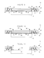
FIGS. 7A and 7B , the build-up ofchip package 10 continues with the aligning and placing of die 12 (i.e., IC) ontoinitial re-distribution layer 16 by way ofadhesive layer 24. Thedie 12 is centered overwindow 26 and is pressed ontoadhesive layer 24, at which time theadhesive layer 24 is fully cured so as to secure the die 12 toinitial re-distribution layer 16, such as by way of a vacuum lamination and pressure bake curing process. As shown inFIGS. 7A and 7B , thedie 12 is sized such that it extends outpast shield element 20. Beneficially, diepads 32 formed around a periphery of the die 12 thus are positioned outside the area ofdie 12 covered byshield element 20, allowing for subsequent electrical connection to thedie pads 32. Additionally, as die 12 extends outpast shield element 20, the die 12 thus rests onadhesive layer 24 and forms anair pocket 36 between the die 12 andshield element 20. Theair gap 36, in conjunction withshield element 20, functions to keep a top surface ofdie 12 clean of contamination. As set forth above inFIG. 5 , avent port 28 is ablated intoadhesive layer 24, with thevent port 28 extending outward fromair pocket 36 to a region ofchip package 10 outside of that covered bydie 12. As thevent port 28 provides fluid communication betweenair gap 36 and an ambient environment outside an area covered bydie 12, pressure in theair gap 36 can thus be controlled, such as pressure that might otherwise increase inair pocket 36 during temperature cycling associated with the build-up process ofchip package 10. - Referring now to
FIG. 8 , upon securing of the die 12 toinitial re-distribution layer 16, theinitial re-distribution layer 16 is patterned to have a plurality ofvias 38 which are drilled through the polymer material forming there-distribution layer 16. According to an exemplary embodiment, thevias 38 are formed by way of a laser ablation or laser drilling process and are formed at positions corresponding to base metal interconnects 22 and to diepads 32, so as to expose the base metal interconnects 22 and diepads 32. Alternatively, it is also recognized thatvias 38 may be formed by way of other methods including: plasma etching, photo-defmition, or mechanical drilling processes. - As further shown in
FIG. 8 , the patterning of theinitial re-distribution layer 16 includes the application of a metal layer/material (e.g., a seed metal and/or copper) applied onto there-distribution layer 16 by way of, for example, a sputtering or electroplating process and the subsequent patterning/etching of the deposited metal layer/material to form metal interconnects 40. According to one embodiment of the invention, the metal layer/material is patterned and etched such that metal interconnects 40 are formed that extend from a top surface ofinitial re-distribution layer 16 and down throughvias 38. Metal interconnects 40 thus form an electrical connection with base metal interconnects 22 and diepads 32. - Referring now to
FIG. 9 , in a next step of the manufacturing technique, one or more additionalre-distribution layers 42 are laminated onto theinitial re-distribution layer 16 on a side ofchip package 10 opposite from which thedie 12 was applied. The additional re-distribution layer(s) 42 are applied to theinitial re-distribution layer 16 through a series of lamination and patterning steps. Anadhesive layer 44 is applied between theinitial re-distribution layer 16 and anadditional re-distribution layer 42 applied thereto. A plurality ofvias 38 is formed in the additional re-distribution layer(s) 42, andmetal interconnects 40 are formed/patterned to extend down throughvias 38 and through the additional re-distribution layer(s) 42, so as to electrically connect eachadditional re-distribution layer 42. While only oneadditional re-distribution layer 42 is shown applied toinitial re-distribution layer 16 to formchip package 10, it is recognized that more re-distribution layers could be applied based on a desired configuration. As shown inFIG. 9 , in further steps of the build-up process, asolder mask 46 can be applied to an outermostadditional re-distribution layer 42 and subsequently patterned so as to provide protection thereto. It is also envisioned that additional components, such as passive devices (not shown), may also be added tochip package 10, with the passive attach being performed whileprotective shield 20 is in place, such that die 12 is protected during such a passive attach. - In a next step of the chip manufacturing technique, and as shown in
FIG. 10 , theinitial re-distribution layer 16, additional re-distribution layer(s) 42, and adhesive layer(s) 44 are laser ablated along apath 48 corresponding to a perimeter ofprotective shield 20, so as to define or separate out aportion 50 of theinitial re-distribution layer 16, additional re-distribution layer(s) 42, and adhesive layer(s) 44. The laser ablation is performed through theinitial re-distribution layer 16, additional re-distribution layer(s) 42, and adhesive layer(s) 44 down toprotective shield 20, where the laser is stopped by theprotective shield 20. Upon completion of the ablation, theportion 50 of theinitial re-distribution layer 16, additional re-distribution layer(s) 42, and adhesive layer(s) 44 positioned aboveprotective shield 20, about which the laser ablation was performed, is removed fromchip package 10 along withprotective shield 20. That is,protective shield 20 sticks toinitial re-distribution layer 16 and tears readily fromadhesive layer 24, such that it can be removed fromchip package 10 along withportion 50 in a single removal step. According to embodiments of the invention,portion 50 andprotective shield 20 can be removed via one of several techniques, such as vacuum pickup or water scrubbing. - As shown in
FIG. 11 , removal ofportion 50 andprotective shield 20 exposes thefront surface 52 of die 12 (i.e., die front) in the completedchip package 10. Beneficially, and based on the presence ofprotective shield 20 above die front 52 (spaced therefrom by air pocket 36) during a duration of the build-up process, thedie front 52 should be clean of contamination. - Beneficially, construction of
chip package 10 according to the technique illustrated inFIGS. 2-9 , provides for a chip package build-up that protects die 12 from contamination during the build-up process. Additionally, the build-up technique provides for manufacturing of achip package 10 having a decreased thickness, limited only be minimum thickness requirements ofdie 12 and re-distribution layer(s) 16, 42. Such a reducedthickness chip package 10 may be configured for use in an imaging device such as an ultra camera, cellular phone camera, or similar sensing device, with the build-up process allowing for mounting of a camera lens (not shown) directly tochip package 10. However, it is also recognized that the reducedthickness chip package 10 could be configured for use in other device types, such as microwave devices, or other devices that would benefit from the manufacturing technique set forth above. - While the invention has been described in detail in connection with only a limited number of embodiments, it should be readily understood that the invention is not limited to such disclosed embodiments. Rather, the invention can be modified to incorporate any number of variations, alterations, substitutions or equivalent arrangements not heretofore described, but which are commensurate with the spirit and scope of the invention. Additionally, while various embodiments of the invention have been described, it is to be understood that aspects of the invention may include only some of the described embodiments. Accordingly, the invention is not to be seen as limited by the foregoing description, but is only limited by the scope of the appended claims.
- Therefore, according to one embodiment of the invention, a chip package includes a base re-distribution layer having an opening formed therein in a center area of the base re-distribution layer, an adhesive layer applied to one side of the base re-distribution layer having a window formed therein free of adhesive material, and a die having a front surface affixed to the base re-distribution layer by way of the adhesive layer, wherein the die is aligned with the window formed in the adhesive layer such that only a perimeter of the front surface of the die is in contact with the adhesive layer. The chip package also includes a plurality of vias and a plurality of metal interconnects formed in the base re-distribution layer to electrically connect the base re-distribution layer to the die and a shield element positioned between the base re-distribution layer and the adhesive layer and generally aligned with the opening formed in the base re-distribution layer and the window of the adhesive layer such that only a perimeter of the shield element is attached to the adhesive layer, with the shield element being separated from the die by an air gap. The shield element is configured to be selectively removable from the adhesive layer so as to expose the front surface of the die.
- According to another embodiment of the invention, a method of forming a chip package includes providing an initial polymer laminate layer, depositing a metallic shield element on one surface of the initial polymer laminate layer so as to cover a portion thereof, and applying an adhesive layer to the initial polymer laminate layer and over the metallic shield element, the adhesive layer having a portion removed therefrom to form a window in the adhesive layer that corresponds substantially to a surface area of the metallic shield element and aligned therewith. The method also includes adhering a die to the initial polymer laminate layer by way of the adhesive layer, with the die being positioned over the window such a perimeter of the die is in contact with the adhesive layer and an air pocket is formed between a center portion of the die and the shield element. The method further includes patterning the initial polymer laminate layer to include a plurality of vias and a plurality of metal interconnects so as to electrically connect the initial polymer laminate layer to the die, defining a portion of the initial polymer laminate layer corresponding to the window in the adhesive layer, and removing the portion of the initial polymer laminate layer and the metallic shield element from the adhesive layer so as to expose a front surface of the die.
- According to yet another embodiment of the invention, a method for manufacturing a chip module includes providing a base re-distribution layer, depositing a shield element on one surface of the base re-distribution layer so as to cover a portion thereof, applying an adhesive layer to the base re-distribution layer and over the shield element, ablating a portion of the adhesive layer in an area adjacent to the shield element so as to expose at least a majority of the shield element, and applying a front surface of a die to the adhesive layer such that the die is aligned with the shield element, wherein a perimeter of the die is in contact with the adhesive layer and a center portion of the die is separated from the shield element by an air gap formed therebetween. The method also includes maintaining the shield element in place during a subsequent patterning of the base re-distribution layer that forms a plurality of vias and a plurality of metal interconnects to electrically connect the base re-distribution layer to the die, ablating a portion of the base re-distribution layer adjacent to the shield element, and removing the shield element and the portion of the base distribution layer so as to expose the front surface of the die.
- Various aspects and embodiments of the present invention are defined by the following numbered clauses:
- 1. A chip package comprising:
- a base re-distribution layer having an opening formed therein in a center area of the base re-distribution layer;
- an adhesive layer applied to one side of the base re-distribution layer, the adhesive layer having a window formed therein free of adhesive material;
- a die having a front surface affixed to the base re-distribution layer by way of the adhesive layer, wherein the die is aligned with the window formed in the adhesive layer such that only a perimeter of the front surface of the die is in contact with the adhesive layer;
- a plurality of vias and a plurality of metal interconnects formed in the base re-distribution layer to electrically connect the base re-distribution layer to the die; and
- a shield element positioned between the base re-distribution layer and the adhesive layer and generally aligned with the opening formed in the base re-distribution layer and the window of the adhesive layer such that only a perimeter of the shield element is attached to the adhesive layer, the shield element being separated from the die by an air gap;
- wherein the shield element is configured to be selectively removable from the adhesive layer so as to expose the front surface of the die.
- 2. The chip package of
clause 1 further comprising a vent port formed in the adhesive layer, the vent port extending out from the air gap and past the perimeter of the die. - 3. The chip package of any preceding clause wherein the vent port is configured to place the air gap in fluid communication with an ambient environment.
- 4. The chip package of any preceding clause further comprising:
- at least one additional re-distribution layer adhered to the base re-distribution layer on a side opposite from the die; and
- a plurality of vias and a plurality of metal interconnects formed in each of the additional re-distribution layers.
- 5. The chip package of any preceding clause wherein the shield element comprises a patterned metallic shield.
- 6. The chip package of any preceding clause wherein the die comprises a camera die configured to form an image sensing area.
- 7. A method of forming a chip package comprising:
- providing an initial polymer laminate layer;
- depositing a metallic shield element on one surface of the initial polymer laminate layer so as to cover a portion thereof;
- applying an adhesive layer to the initial polymer laminate layer and over the metallic shield element, the adhesive layer having a portion removed therefrom to form a window in the adhesive layer that corresponds substantially to a surface area of the metallic shield element and aligned therewith;
- adhering a die to the initial polymer laminate layer by way of the adhesive layer, the die being positioned over the window such a perimeter of the die is in contact with the adhesive layer and an air pocket is formed between a center portion of the die and the shield element;
- patterning the initial polymer laminate layer to include a plurality of vias and a plurality of metal interconnects, so as to electrically connect the initial polymer laminate layer to the die;
- defining a portion of the initial polymer laminate layer corresponding to the window in the adhesive layer; and
- removing the portion of the initial polymer laminate layer and the metallic shield element from the adhesive layer so as to expose a front surface of the die.
- 8. The method of any preceding clause further comprising laser ablating through the adhesive layer to form the window therein, the metallic shield element acting as a back stop during the laser ablation.
- 9. The method of any preceding clause further comprising laser ablating a vent port in the adhesive layer, the vent port extending out from the window formed in the adhesive layer and past the perimeter of the die to be placed on the adhesive layer.
- 10. The method of any preceding clause further comprising partially curing the adhesive layer along a perimeter of the window so as to prevent adhesive material from encroaching into the window.
- 11. The method of any preceding clause wherein defining the portion of the initial polymer laminate layer comprises laser ablating down through the initial polymer laminate layer to the metallic shield element.
- 12. The method of any preceding clause wherein removing the portion of the initial polymer laminate layer and the metallic shield element comprises performing one of a vacuum pick-up and a water scrubbing.
- 13. The method of any preceding clause further comprising:
- adhering at least one additional polymer layer to the initial polymer laminate layer; and
- patterning each of the at least one additional polymer laminate layers to include a plurality of vias and a plurality of metal interconnects.
- 14. A method for manufacturing a chip module comprising:
- providing a base re-distribution layer;
- depositing a shield element on one surface of the base re-distribution layer so as to cover a portion thereof;
- applying an adhesive layer to the base re-distribution layer and over the shield element;
- ablating a portion of the adhesive layer in an area adjacent to the shield element so as to expose at least a majority of the shield element;
- applying a front surface of a die to the adhesive layer such that the die is aligned with the shield element, wherein a perimeter of the die is in contact with the adhesive layer and a center portion of the die is separated from the shield element by an air gap formed therebetween;
- maintaining the shield element in place during a subsequent patterning of the base re-distribution layer, the patterning forming a plurality of vias and a plurality of metal interconnects to electrically connect the base re-distribution layer to the die;
- ablating a portion of the base re-distribution layer adjacent to the shield element; and
- removing the shield element and the portion of the base distribution layer so as to expose the front surface of the die.
- 15. The method of any preceding clause wherein ablating the adhesive layer comprises laser ablating through the adhesive layer to the shield element.
- 16. The method of any preceding clause further comprising forming a metallic vent base on the one surface of the base re-distribution layer that extends out from the shield element.
- 17. The method of any preceding clause further comprising laser ablating a vent port in the adhesive layer using the vent base as a backstop, the vent port extending out from the air gap and past the perimeter of the die to be placed on the adhesive layer so as to place the air gap in fluid communication with an ambient environment.
- 18. The method of any preceding clause further comprising, upon ablation of the adhesive layer, partially curing an edge of the adhesive layer along the area adjacent to the shield element.
- 19. The method of any preceding clause further comprising:
- adhering at least one additional re-distribution layer to the base re-distribution layer; and
- patterning each of the at least one additional re-distribution layers to include a plurality of vias and a plurality of metal interconnects;
- wherein a portion of the at least one additional re-distribution layer is ablated adjacent to the shield element along with ablating of the portion of the base re-distribution layer, and wherein the portion of the at least one additional re-distribution layer, the portion of the base re-distribution layer, and the shield element are removed so as to expose the front surface of the die.
- 20. The method of any preceding clause wherein ablating the base re-distribution layer comprises laser cutting around a perimeter of the portion of the base re-distribution layer adjacent to the shield element and down to the shield element, such that the portion of the base re-distribution layer and the shield element can be removed to expose the front surface of the die.
Claims (10)
- A chip package (10) comprising:a base re-distribution layer (16) having an opening formed therein in a center area of the base re-distribution layer (16);an adhesive layer (24) applied to one side of the base re-distribution layer (16), the adhesive layer (24) having a window (26) formed therein free of adhesive material;a die (12) having a front surface (52) affixed to the base re-distribution layer (16) by way of the adhesive layer (24), wherein the die (12) is aligned with the window (26) formed in the adhesive layer (24) such that only a perimeter of the front surface (52) of the die (12) is in contact with the adhesive layer (24);a plurality of vias (38) and a plurality of metal interconnects (40) formed in the base re-distribution layer (16) to electrically connect the base re-distribution layer (16) to the die (12); anda shield element (20) positioned between the base re-distribution layer (16) and the adhesive layer (24) and generally aligned with the opening formed in the base re-distribution layer (16) and the window (26) of the adhesive layer (24) such that only a perimeter of the shield element (20) is attached to the adhesive layer (24), the shield element (20) being separated from the die (12) by an air gap (36);wherein the shield element (20) is configured to be selectively removable from the adhesive layer (24) so as to expose the front surface (52) of the die (12).
- The chip package (10) of claim 1 further comprising a vent port (28) formed in the adhesive layer (24), the vent port (28) extending out from the air gap (36) and past the perimeter of the die (12).
- The chip package (10) of claim 2 wherein the vent port (28) is configured to place the air gap (36) in fluid communication with an ambient environment.
- The chip package (10) of claim 2 or claim 3 further comprising a metallic vent base (21) positioned below the vent port (28) to provide for formation of the vent port (28).
- The chip package (10) of any preceding claim further comprising:at least one additional re-distribution layer (42) adhered to the base re-distribution layer (16) on a side opposite from the die (12); anda plurality of vias (38) and a plurality of metal interconnects (40) formed in each of the additional re-distribution layers (42).
- The chip package (10) of any preceding claim further comprising a solder mask (46) positioned on a top-most additional re-distribution layer (42).
- The chip package (10) of any preceding claim wherein the shield element (20) comprises a patterned metallic shield.
- The chip package (10) of any preceding claim wherein the die (12) comprises a camera die configured to form an image sensing area.
- The chip package (10) of any preceding claim wherein the shield element (20) has an area smaller than an area of the die (12).
- The chip package (10) of any preceding claim wherein the die (12) further comprises a plurality of die pads (32) formed around a periphery thereof, the plurality of die pads (32) being positioned outside an area of die (12) covered by shield element (20).
Applications Claiming Priority (1)
| Application Number | Priority Date | Filing Date | Title |
|---|---|---|---|
| US12/843,606 US8623699B2 (en) | 2010-07-26 | 2010-07-26 | Method of chip package build-up |
Publications (3)
| Publication Number | Publication Date |
|---|---|
| EP2434539A2 true EP2434539A2 (en) | 2012-03-28 |
| EP2434539A3 EP2434539A3 (en) | 2018-01-17 |
| EP2434539B1 EP2434539B1 (en) | 2022-01-26 |
Family
ID=44532619
Family Applications (1)
| Application Number | Title | Priority Date | Filing Date |
|---|---|---|---|
| EP11174096.5A Active EP2434539B1 (en) | 2010-07-26 | 2011-07-15 | System and method of chip package build-up |
Country Status (6)
| Country | Link |
|---|---|
| US (2) | US8623699B2 (en) |
| EP (1) | EP2434539B1 (en) |
| JP (1) | JP5806534B2 (en) |
| KR (1) | KR101846548B1 (en) |
| CN (1) | CN102347301B (en) |
| TW (1) | TWI536509B (en) |
Cited By (1)
| Publication number | Priority date | Publication date | Assignee | Title |
|---|---|---|---|---|
| EP2674970A3 (en) * | 2012-06-15 | 2014-03-26 | General Electric Company | Integrated circuit build-up package and method of manufacturing the same with adhesive die mounting to a dielectric layer |
Families Citing this family (7)
| Publication number | Priority date | Publication date | Assignee | Title |
|---|---|---|---|---|
| US8618652B2 (en) | 2010-04-16 | 2013-12-31 | Intel Corporation | Forming functionalized carrier structures with coreless packages |
| US8969176B2 (en) * | 2010-12-03 | 2015-03-03 | Raytheon Company | Laminated transferable interconnect for microelectronic package |
| US8658473B2 (en) * | 2012-03-27 | 2014-02-25 | General Electric Company | Ultrathin buried die module and method of manufacturing thereof |
| US9324664B2 (en) * | 2013-02-22 | 2016-04-26 | Unimicron Technology Corp. | Embedded chip package structure |
| KR102647496B1 (en) * | 2015-09-30 | 2024-03-15 | 스카이워크스 솔루션즈, 인코포레이티드 | Devices and methods for manufacturing shielded modules |
| CN110164839B (en) * | 2019-05-27 | 2020-01-31 | 广东工业大学 | Fan-out type packaging structure and method for embedding and transferring high-density lines |
| CN115642092B (en) * | 2022-09-13 | 2023-11-17 | 盛合晶微半导体(江阴)有限公司 | System-level fan-out type packaging structure and manufacturing method thereof |
Family Cites Families (13)
| Publication number | Priority date | Publication date | Assignee | Title |
|---|---|---|---|---|
| US5355102A (en) * | 1990-04-05 | 1994-10-11 | General Electric Company | HDI impedance matched microwave circuit assembly |
| US5401687A (en) * | 1993-04-15 | 1995-03-28 | Martin Marietta Corporation | Process for high density interconnection of substrates and integrated circuit chips containing sensitive structures |
| US5635762A (en) * | 1993-05-18 | 1997-06-03 | U.S. Philips Corporation | Flip chip semiconductor device with dual purpose metallized ground conductor |
| US5527741A (en) * | 1994-10-11 | 1996-06-18 | Martin Marietta Corporation | Fabrication and structures of circuit modules with flexible interconnect layers |
| US5561085A (en) * | 1994-12-19 | 1996-10-01 | Martin Marietta Corporation | Structure for protecting air bridges on semiconductor chips from damage |
| US6255137B1 (en) * | 1999-07-01 | 2001-07-03 | Lockheed Martin Corp. | Method for making air pockets in an HDI context |
| US6671948B2 (en) * | 2000-12-18 | 2004-01-06 | General Electric Company | Interconnection method using an etch stop |
| US6964881B2 (en) * | 2002-08-27 | 2005-11-15 | Micron Technology, Inc. | Multi-chip wafer level system packages and methods of forming same |
| US7880297B2 (en) * | 2007-12-31 | 2011-02-01 | Mediatek Inc. | Semiconductor chip having conductive member for reducing localized voltage drop |
| US8259454B2 (en) | 2008-04-14 | 2012-09-04 | General Electric Company | Interconnect structure including hybrid frame panel |
| US20110156261A1 (en) * | 2009-03-24 | 2011-06-30 | Christopher James Kapusta | Integrated circuit package and method of making same |
| US8319318B2 (en) * | 2010-04-06 | 2012-11-27 | Intel Corporation | Forming metal filled die back-side film for electromagnetic interference shielding with coreless packages |
| US8618652B2 (en) * | 2010-04-16 | 2013-12-31 | Intel Corporation | Forming functionalized carrier structures with coreless packages |
-
2010
- 2010-07-26 US US12/843,606 patent/US8623699B2/en active Active
-
2011
- 2011-07-15 EP EP11174096.5A patent/EP2434539B1/en active Active
- 2011-07-20 JP JP2011158524A patent/JP5806534B2/en active Active
- 2011-07-26 TW TW100126447A patent/TWI536509B/en active
- 2011-07-26 KR KR1020110074112A patent/KR101846548B1/en active Active
- 2011-07-26 CN CN201110264934.2A patent/CN102347301B/en active Active
-
2013
- 2013-12-23 US US14/138,333 patent/US8829690B2/en active Active
Non-Patent Citations (1)
| Title |
|---|
| None |
Cited By (3)
| Publication number | Priority date | Publication date | Assignee | Title |
|---|---|---|---|---|
| EP2674970A3 (en) * | 2012-06-15 | 2014-03-26 | General Electric Company | Integrated circuit build-up package and method of manufacturing the same with adhesive die mounting to a dielectric layer |
| US9117813B2 (en) | 2012-06-15 | 2015-08-25 | General Electric Company | Integrated circuit package and method of making same |
| US9613932B2 (en) | 2012-06-15 | 2017-04-04 | General Electric Company | Integrated circuit package and method of making same |
Also Published As
| Publication number | Publication date |
|---|---|
| CN102347301A (en) | 2012-02-08 |
| US8829690B2 (en) | 2014-09-09 |
| JP5806534B2 (en) | 2015-11-10 |
| US20140110866A1 (en) | 2014-04-24 |
| TW201216420A (en) | 2012-04-16 |
| KR20120010985A (en) | 2012-02-06 |
| CN102347301B (en) | 2015-11-25 |
| EP2434539A3 (en) | 2018-01-17 |
| TWI536509B (en) | 2016-06-01 |
| US8623699B2 (en) | 2014-01-07 |
| JP2012069918A (en) | 2012-04-05 |
| EP2434539B1 (en) | 2022-01-26 |
| US20120018857A1 (en) | 2012-01-26 |
| KR101846548B1 (en) | 2018-04-06 |
Similar Documents
| Publication | Publication Date | Title |
|---|---|---|
| US8829690B2 (en) | System of chip package build-up | |
| KR102566839B1 (en) | Integrated circuit packaging system with shielding and method of manufacture thereof | |
| US8432022B1 (en) | Shielded embedded electronic component substrate fabrication method and structure | |
| US20110018076A1 (en) | MEMS Component, Method for Producing a MEMS Component, and Method for Handling a MEMS Component | |
| US7811857B2 (en) | Method of manufacturing semiconductor device | |
| US20100110656A1 (en) | Chip package and manufacturing method thereof | |
| KR100852597B1 (en) | Manufacturing Method of Semiconductor Device | |
| WO2008018524A1 (en) | Semiconductor device and its manufacturing method | |
| US9966400B2 (en) | Photosensitive module and method for forming the same | |
| TW201227937A (en) | Image sensor chip package and method for forming the same | |
| US20040101995A1 (en) | Method for manufacturing circuit devices | |
| CN113838751A (en) | A method of cutting package substrate unit | |
| EP2040294B1 (en) | Method of manufacturing a semiconductor device | |
| US8338918B2 (en) | Method for manufacturing a semiconductor device, method for detecting a semiconductor substrate and semiconductor chip package | |
| US20130017651A1 (en) | Method for manufacturing a semiconductor package | |
| US20160218133A1 (en) | Photosensitive module and method for forming the same | |
| KR20060116894A (en) | Surface acoustic wave device package and manufacturing method thereof | |
| JP4619308B2 (en) | Semiconductor device manufacturing method and supporting tape | |
| JP2008047786A (en) | Insulating film formation method | |
| CN119050165A (en) | Sensor package and method of forming the same | |
| JP2010147292A (en) | Method of manufacturing semiconductor device |
Legal Events
| Date | Code | Title | Description |
|---|---|---|---|
| PUAI | Public reference made under article 153(3) epc to a published international application that has entered the european phase |
Free format text: ORIGINAL CODE: 0009012 |
|
| AK | Designated contracting states |
Kind code of ref document: A2 Designated state(s): AL AT BE BG CH CY CZ DE DK EE ES FI FR GB GR HR HU IE IS IT LI LT LU LV MC MK MT NL NO PL PT RO RS SE SI SK SM TR |
|
| AX | Request for extension of the european patent |
Extension state: BA ME |
|
| PUAL | Search report despatched |
Free format text: ORIGINAL CODE: 0009013 |
|
| AK | Designated contracting states |
Kind code of ref document: A3 Designated state(s): AL AT BE BG CH CY CZ DE DK EE ES FI FR GB GR HR HU IE IS IT LI LT LU LV MC MK MT NL NO PL PT RO RS SE SI SK SM TR |
|
| AX | Request for extension of the european patent |
Extension state: BA ME |
|
| RIC1 | Information provided on ipc code assigned before grant |
Ipc: H01L 23/48 20060101ALI20171212BHEP Ipc: H01L 21/60 20060101AFI20171212BHEP |
|
| STAA | Information on the status of an ep patent application or granted ep patent |
Free format text: STATUS: REQUEST FOR EXAMINATION WAS MADE |
|
| 17P | Request for examination filed |
Effective date: 20180717 |
|
| RBV | Designated contracting states (corrected) |
Designated state(s): AL AT BE BG CH CY CZ DE DK EE ES FI FR GB GR HR HU IE IS IT LI LT LU LV MC MK MT NL NO PL PT RO RS SE SI SK SM TR |
|
| GRAP | Despatch of communication of intention to grant a patent |
Free format text: ORIGINAL CODE: EPIDOSNIGR1 |
|
| STAA | Information on the status of an ep patent application or granted ep patent |
Free format text: STATUS: GRANT OF PATENT IS INTENDED |
|
| INTG | Intention to grant announced |
Effective date: 20210816 |
|
| GRAS | Grant fee paid |
Free format text: ORIGINAL CODE: EPIDOSNIGR3 |
|
| GRAA | (expected) grant |
Free format text: ORIGINAL CODE: 0009210 |
|
| STAA | Information on the status of an ep patent application or granted ep patent |
Free format text: STATUS: THE PATENT HAS BEEN GRANTED |
|
| AK | Designated contracting states |
Kind code of ref document: B1 Designated state(s): AL AT BE BG CH CY CZ DE DK EE ES FI FR GB GR HR HU IE IS IT LI LT LU LV MC MK MT NL NO PL PT RO RS SE SI SK SM TR |
|
| REG | Reference to a national code |
Ref country code: GB Ref legal event code: FG4D |
|
| REG | Reference to a national code |
Ref country code: CH Ref legal event code: EP |
|
| REG | Reference to a national code |
Ref country code: AT Ref legal event code: REF Ref document number: 1465934 Country of ref document: AT Kind code of ref document: T Effective date: 20220215 |
|
| REG | Reference to a national code |
Ref country code: IE Ref legal event code: FG4D |
|
| REG | Reference to a national code |
Ref country code: DE Ref legal event code: R096 Ref document number: 602011072443 Country of ref document: DE |
|
| REG | Reference to a national code |
Ref country code: LT Ref legal event code: MG9D |
|
| REG | Reference to a national code |
Ref country code: NL Ref legal event code: MP Effective date: 20220126 |
|
| REG | Reference to a national code |
Ref country code: AT Ref legal event code: MK05 Ref document number: 1465934 Country of ref document: AT Kind code of ref document: T Effective date: 20220126 |
|
| PG25 | Lapsed in a contracting state [announced via postgrant information from national office to epo] |
Ref country code: NL Free format text: LAPSE BECAUSE OF FAILURE TO SUBMIT A TRANSLATION OF THE DESCRIPTION OR TO PAY THE FEE WITHIN THE PRESCRIBED TIME-LIMIT Effective date: 20220126 |
|
| PG25 | Lapsed in a contracting state [announced via postgrant information from national office to epo] |
Ref country code: SE Free format text: LAPSE BECAUSE OF FAILURE TO SUBMIT A TRANSLATION OF THE DESCRIPTION OR TO PAY THE FEE WITHIN THE PRESCRIBED TIME-LIMIT Effective date: 20220126 Ref country code: RS Free format text: LAPSE BECAUSE OF FAILURE TO SUBMIT A TRANSLATION OF THE DESCRIPTION OR TO PAY THE FEE WITHIN THE PRESCRIBED TIME-LIMIT Effective date: 20220126 Ref country code: PT Free format text: LAPSE BECAUSE OF FAILURE TO SUBMIT A TRANSLATION OF THE DESCRIPTION OR TO PAY THE FEE WITHIN THE PRESCRIBED TIME-LIMIT Effective date: 20220526 Ref country code: NO Free format text: LAPSE BECAUSE OF FAILURE TO SUBMIT A TRANSLATION OF THE DESCRIPTION OR TO PAY THE FEE WITHIN THE PRESCRIBED TIME-LIMIT Effective date: 20220426 Ref country code: LT Free format text: LAPSE BECAUSE OF FAILURE TO SUBMIT A TRANSLATION OF THE DESCRIPTION OR TO PAY THE FEE WITHIN THE PRESCRIBED TIME-LIMIT Effective date: 20220126 Ref country code: HR Free format text: LAPSE BECAUSE OF FAILURE TO SUBMIT A TRANSLATION OF THE DESCRIPTION OR TO PAY THE FEE WITHIN THE PRESCRIBED TIME-LIMIT Effective date: 20220126 Ref country code: ES Free format text: LAPSE BECAUSE OF FAILURE TO SUBMIT A TRANSLATION OF THE DESCRIPTION OR TO PAY THE FEE WITHIN THE PRESCRIBED TIME-LIMIT Effective date: 20220126 Ref country code: BG Free format text: LAPSE BECAUSE OF FAILURE TO SUBMIT A TRANSLATION OF THE DESCRIPTION OR TO PAY THE FEE WITHIN THE PRESCRIBED TIME-LIMIT Effective date: 20220426 |
|
| PG25 | Lapsed in a contracting state [announced via postgrant information from national office to epo] |
Ref country code: PL Free format text: LAPSE BECAUSE OF FAILURE TO SUBMIT A TRANSLATION OF THE DESCRIPTION OR TO PAY THE FEE WITHIN THE PRESCRIBED TIME-LIMIT Effective date: 20220126 Ref country code: LV Free format text: LAPSE BECAUSE OF FAILURE TO SUBMIT A TRANSLATION OF THE DESCRIPTION OR TO PAY THE FEE WITHIN THE PRESCRIBED TIME-LIMIT Effective date: 20220126 Ref country code: GR Free format text: LAPSE BECAUSE OF FAILURE TO SUBMIT A TRANSLATION OF THE DESCRIPTION OR TO PAY THE FEE WITHIN THE PRESCRIBED TIME-LIMIT Effective date: 20220427 Ref country code: FI Free format text: LAPSE BECAUSE OF FAILURE TO SUBMIT A TRANSLATION OF THE DESCRIPTION OR TO PAY THE FEE WITHIN THE PRESCRIBED TIME-LIMIT Effective date: 20220126 Ref country code: AT Free format text: LAPSE BECAUSE OF FAILURE TO SUBMIT A TRANSLATION OF THE DESCRIPTION OR TO PAY THE FEE WITHIN THE PRESCRIBED TIME-LIMIT Effective date: 20220126 |
|
| PG25 | Lapsed in a contracting state [announced via postgrant information from national office to epo] |
Ref country code: IS Free format text: LAPSE BECAUSE OF FAILURE TO SUBMIT A TRANSLATION OF THE DESCRIPTION OR TO PAY THE FEE WITHIN THE PRESCRIBED TIME-LIMIT Effective date: 20220526 |
|
| REG | Reference to a national code |
Ref country code: DE Ref legal event code: R097 Ref document number: 602011072443 Country of ref document: DE |
|
| PG25 | Lapsed in a contracting state [announced via postgrant information from national office to epo] |
Ref country code: SM Free format text: LAPSE BECAUSE OF FAILURE TO SUBMIT A TRANSLATION OF THE DESCRIPTION OR TO PAY THE FEE WITHIN THE PRESCRIBED TIME-LIMIT Effective date: 20220126 Ref country code: SK Free format text: LAPSE BECAUSE OF FAILURE TO SUBMIT A TRANSLATION OF THE DESCRIPTION OR TO PAY THE FEE WITHIN THE PRESCRIBED TIME-LIMIT Effective date: 20220126 Ref country code: RO Free format text: LAPSE BECAUSE OF FAILURE TO SUBMIT A TRANSLATION OF THE DESCRIPTION OR TO PAY THE FEE WITHIN THE PRESCRIBED TIME-LIMIT Effective date: 20220126 Ref country code: EE Free format text: LAPSE BECAUSE OF FAILURE TO SUBMIT A TRANSLATION OF THE DESCRIPTION OR TO PAY THE FEE WITHIN THE PRESCRIBED TIME-LIMIT Effective date: 20220126 Ref country code: DK Free format text: LAPSE BECAUSE OF FAILURE TO SUBMIT A TRANSLATION OF THE DESCRIPTION OR TO PAY THE FEE WITHIN THE PRESCRIBED TIME-LIMIT Effective date: 20220126 Ref country code: CZ Free format text: LAPSE BECAUSE OF FAILURE TO SUBMIT A TRANSLATION OF THE DESCRIPTION OR TO PAY THE FEE WITHIN THE PRESCRIBED TIME-LIMIT Effective date: 20220126 |
|
| PG25 | Lapsed in a contracting state [announced via postgrant information from national office to epo] |
Ref country code: AL Free format text: LAPSE BECAUSE OF FAILURE TO SUBMIT A TRANSLATION OF THE DESCRIPTION OR TO PAY THE FEE WITHIN THE PRESCRIBED TIME-LIMIT Effective date: 20220126 |
|
| PLBE | No opposition filed within time limit |
Free format text: ORIGINAL CODE: 0009261 |
|
| STAA | Information on the status of an ep patent application or granted ep patent |
Free format text: STATUS: NO OPPOSITION FILED WITHIN TIME LIMIT |
|
| 26N | No opposition filed |
Effective date: 20221027 |
|
| PG25 | Lapsed in a contracting state [announced via postgrant information from national office to epo] |
Ref country code: SI Free format text: LAPSE BECAUSE OF FAILURE TO SUBMIT A TRANSLATION OF THE DESCRIPTION OR TO PAY THE FEE WITHIN THE PRESCRIBED TIME-LIMIT Effective date: 20220126 Ref country code: MC Free format text: LAPSE BECAUSE OF FAILURE TO SUBMIT A TRANSLATION OF THE DESCRIPTION OR TO PAY THE FEE WITHIN THE PRESCRIBED TIME-LIMIT Effective date: 20220126 |
|
| REG | Reference to a national code |
Ref country code: CH Ref legal event code: PL |
|
| REG | Reference to a national code |
Ref country code: BE Ref legal event code: MM Effective date: 20220731 |
|
| PG25 | Lapsed in a contracting state [announced via postgrant information from national office to epo] |
Ref country code: LU Free format text: LAPSE BECAUSE OF NON-PAYMENT OF DUE FEES Effective date: 20220715 Ref country code: LI Free format text: LAPSE BECAUSE OF NON-PAYMENT OF DUE FEES Effective date: 20220731 Ref country code: CH Free format text: LAPSE BECAUSE OF NON-PAYMENT OF DUE FEES Effective date: 20220731 |
|
| PG25 | Lapsed in a contracting state [announced via postgrant information from national office to epo] |
Ref country code: BE Free format text: LAPSE BECAUSE OF NON-PAYMENT OF DUE FEES Effective date: 20220731 |
|
| PG25 | Lapsed in a contracting state [announced via postgrant information from national office to epo] |
Ref country code: IT Free format text: LAPSE BECAUSE OF FAILURE TO SUBMIT A TRANSLATION OF THE DESCRIPTION OR TO PAY THE FEE WITHIN THE PRESCRIBED TIME-LIMIT Effective date: 20220126 Ref country code: IE Free format text: LAPSE BECAUSE OF NON-PAYMENT OF DUE FEES Effective date: 20220715 |
|
| PG25 | Lapsed in a contracting state [announced via postgrant information from national office to epo] |
Ref country code: HU Free format text: LAPSE BECAUSE OF FAILURE TO SUBMIT A TRANSLATION OF THE DESCRIPTION OR TO PAY THE FEE WITHIN THE PRESCRIBED TIME-LIMIT; INVALID AB INITIO Effective date: 20110715 |
|
| PG25 | Lapsed in a contracting state [announced via postgrant information from national office to epo] |
Ref country code: MK Free format text: LAPSE BECAUSE OF FAILURE TO SUBMIT A TRANSLATION OF THE DESCRIPTION OR TO PAY THE FEE WITHIN THE PRESCRIBED TIME-LIMIT Effective date: 20220126 Ref country code: CY Free format text: LAPSE BECAUSE OF FAILURE TO SUBMIT A TRANSLATION OF THE DESCRIPTION OR TO PAY THE FEE WITHIN THE PRESCRIBED TIME-LIMIT Effective date: 20220126 |
|
| PG25 | Lapsed in a contracting state [announced via postgrant information from national office to epo] |
Ref country code: TR Free format text: LAPSE BECAUSE OF FAILURE TO SUBMIT A TRANSLATION OF THE DESCRIPTION OR TO PAY THE FEE WITHIN THE PRESCRIBED TIME-LIMIT Effective date: 20220126 |
|
| PG25 | Lapsed in a contracting state [announced via postgrant information from national office to epo] |
Ref country code: MT Free format text: LAPSE BECAUSE OF FAILURE TO SUBMIT A TRANSLATION OF THE DESCRIPTION OR TO PAY THE FEE WITHIN THE PRESCRIBED TIME-LIMIT Effective date: 20220126 |
|
| PGFP | Annual fee paid to national office [announced via postgrant information from national office to epo] |
Ref country code: GB Payment date: 20250619 Year of fee payment: 15 |
|
| PGFP | Annual fee paid to national office [announced via postgrant information from national office to epo] |
Ref country code: FR Payment date: 20250619 Year of fee payment: 15 |
|
| PGFP | Annual fee paid to national office [announced via postgrant information from national office to epo] |
Ref country code: DE Payment date: 20250620 Year of fee payment: 15 |
|
| REG | Reference to a national code |
Ref country code: DE Ref legal event code: R079 Ref document number: 602011072443 Country of ref document: DE Free format text: PREVIOUS MAIN CLASS: H01L0021600000 Ipc: H10W0070010000 |