EP2434031A1 - Weiße Zierverkleidung, Dekoartikel und Verfahren - Google Patents
Weiße Zierverkleidung, Dekoartikel und Verfahren Download PDFInfo
- Publication number
- EP2434031A1 EP2434031A1 EP10193388A EP10193388A EP2434031A1 EP 2434031 A1 EP2434031 A1 EP 2434031A1 EP 10193388 A EP10193388 A EP 10193388A EP 10193388 A EP10193388 A EP 10193388A EP 2434031 A1 EP2434031 A1 EP 2434031A1
- Authority
- EP
- European Patent Office
- Prior art keywords
- layer
- rough
- substrate
- depositing
- decorative
- Prior art date
- Legal status (The legal status is an assumption and is not a legal conclusion. Google has not performed a legal analysis and makes no representation as to the accuracy of the status listed.)
- Granted
Links
- 238000000034 method Methods 0.000 title claims abstract description 35
- 239000010410 layer Substances 0.000 claims abstract description 81
- 239000000758 substrate Substances 0.000 claims abstract description 34
- 238000000151 deposition Methods 0.000 claims abstract description 29
- 238000005240 physical vapour deposition Methods 0.000 claims abstract description 15
- BQCADISMDOOEFD-UHFFFAOYSA-N Silver Chemical group [Ag] BQCADISMDOOEFD-UHFFFAOYSA-N 0.000 claims abstract description 12
- 229910052709 silver Inorganic materials 0.000 claims abstract description 12
- 239000004332 silver Substances 0.000 claims abstract description 12
- 229910052782 aluminium Inorganic materials 0.000 claims abstract description 11
- XAGFODPZIPBFFR-UHFFFAOYSA-N aluminium Chemical compound [Al] XAGFODPZIPBFFR-UHFFFAOYSA-N 0.000 claims abstract description 11
- 238000004544 sputter deposition Methods 0.000 claims abstract description 11
- 239000011241 protective layer Substances 0.000 claims abstract description 7
- 238000009500 colour coating Methods 0.000 claims abstract 2
- 238000000576 coating method Methods 0.000 claims description 30
- 239000011248 coating agent Substances 0.000 claims description 27
- 230000008021 deposition Effects 0.000 claims description 15
- XLOMVQKBTHCTTD-UHFFFAOYSA-N Zinc monoxide Chemical compound [Zn]=O XLOMVQKBTHCTTD-UHFFFAOYSA-N 0.000 claims description 7
- GWEVSGVZZGPLCZ-UHFFFAOYSA-N Titan oxide Chemical compound O=[Ti]=O GWEVSGVZZGPLCZ-UHFFFAOYSA-N 0.000 claims description 5
- 239000000203 mixture Substances 0.000 claims description 5
- 229910018072 Al 2 O 3 Inorganic materials 0.000 claims description 4
- OKTJSMMVPCPJKN-UHFFFAOYSA-N Carbon Chemical compound [C] OKTJSMMVPCPJKN-UHFFFAOYSA-N 0.000 claims description 4
- 229910052799 carbon Inorganic materials 0.000 claims description 4
- 229910017083 AlN Inorganic materials 0.000 claims description 3
- 229910004298 SiO 2 Inorganic materials 0.000 claims description 3
- 229910010413 TiO 2 Inorganic materials 0.000 claims description 3
- GEIAQOFPUVMAGM-UHFFFAOYSA-N ZrO Inorganic materials [Zr]=O GEIAQOFPUVMAGM-UHFFFAOYSA-N 0.000 claims description 3
- PNEYBMLMFCGWSK-UHFFFAOYSA-N aluminium oxide Inorganic materials [O-2].[O-2].[O-2].[Al+3].[Al+3] PNEYBMLMFCGWSK-UHFFFAOYSA-N 0.000 claims description 3
- 229910052593 corundum Inorganic materials 0.000 claims description 3
- 229910001845 yogo sapphire Inorganic materials 0.000 claims description 3
- 229910017109 AlON Inorganic materials 0.000 claims description 2
- 229910052804 chromium Inorganic materials 0.000 claims description 2
- 238000005034 decoration Methods 0.000 claims description 2
- 229910052719 titanium Inorganic materials 0.000 claims description 2
- VYPSYNLAJGMNEJ-UHFFFAOYSA-N Silicium dioxide Chemical compound O=[Si]=O VYPSYNLAJGMNEJ-UHFFFAOYSA-N 0.000 claims 2
- MCMNRKCIXSYSNV-UHFFFAOYSA-N Zirconium dioxide Chemical compound O=[Zr]=O MCMNRKCIXSYSNV-UHFFFAOYSA-N 0.000 claims 2
- PIGFYZPCRLYGLF-UHFFFAOYSA-N Aluminum nitride Chemical compound [Al]#N PIGFYZPCRLYGLF-UHFFFAOYSA-N 0.000 claims 1
- 229910052681 coesite Inorganic materials 0.000 claims 1
- 229910052906 cristobalite Inorganic materials 0.000 claims 1
- PUIYMUZLKQOUOZ-UHFFFAOYSA-N isoproturon Chemical compound CC(C)C1=CC=C(NC(=O)N(C)C)C=C1 PUIYMUZLKQOUOZ-UHFFFAOYSA-N 0.000 claims 1
- 239000000377 silicon dioxide Substances 0.000 claims 1
- 235000012239 silicon dioxide Nutrition 0.000 claims 1
- 229910052682 stishovite Inorganic materials 0.000 claims 1
- 229910052905 tridymite Inorganic materials 0.000 claims 1
- 238000005507 spraying Methods 0.000 description 7
- KDLHZDBZIXYQEI-UHFFFAOYSA-N Palladium Chemical compound [Pd] KDLHZDBZIXYQEI-UHFFFAOYSA-N 0.000 description 5
- 238000004519 manufacturing process Methods 0.000 description 4
- 239000000463 material Substances 0.000 description 4
- 238000005137 deposition process Methods 0.000 description 3
- 239000007789 gas Substances 0.000 description 3
- 229910052751 metal Inorganic materials 0.000 description 3
- 239000002184 metal Substances 0.000 description 3
- 229910052763 palladium Inorganic materials 0.000 description 3
- 239000010948 rhodium Substances 0.000 description 3
- 239000000126 substance Substances 0.000 description 3
- 238000005494 tarnishing Methods 0.000 description 3
- XKRFYHLGVUSROY-UHFFFAOYSA-N Argon Chemical compound [Ar] XKRFYHLGVUSROY-UHFFFAOYSA-N 0.000 description 2
- 239000012298 atmosphere Substances 0.000 description 2
- 210000003298 dental enamel Anatomy 0.000 description 2
- 150000002500 ions Chemical class 0.000 description 2
- 238000001755 magnetron sputter deposition Methods 0.000 description 2
- 150000002739 metals Chemical class 0.000 description 2
- 239000011859 microparticle Substances 0.000 description 2
- 239000002245 particle Substances 0.000 description 2
- 239000000049 pigment Substances 0.000 description 2
- BASFCYQUMIYNBI-UHFFFAOYSA-N platinum Chemical compound [Pt] BASFCYQUMIYNBI-UHFFFAOYSA-N 0.000 description 2
- 229910052703 rhodium Inorganic materials 0.000 description 2
- MHOVAHRLVXNVSD-UHFFFAOYSA-N rhodium atom Chemical compound [Rh] MHOVAHRLVXNVSD-UHFFFAOYSA-N 0.000 description 2
- 239000011787 zinc oxide Substances 0.000 description 2
- 239000004923 Acrylic lacquer Substances 0.000 description 1
- RYGMFSIKBFXOCR-UHFFFAOYSA-N Copper Chemical compound [Cu] RYGMFSIKBFXOCR-UHFFFAOYSA-N 0.000 description 1
- 239000000020 Nitrocellulose Substances 0.000 description 1
- 206010030924 Optic ischaemic neuropathy Diseases 0.000 description 1
- 241001085205 Prenanthella exigua Species 0.000 description 1
- 239000000956 alloy Substances 0.000 description 1
- 229910045601 alloy Inorganic materials 0.000 description 1
- 229910052786 argon Inorganic materials 0.000 description 1
- 239000012300 argon atmosphere Substances 0.000 description 1
- 230000015572 biosynthetic process Effects 0.000 description 1
- 229910000420 cerium oxide Inorganic materials 0.000 description 1
- 238000004140 cleaning Methods 0.000 description 1
- 239000003086 colorant Substances 0.000 description 1
- 229920000547 conjugated polymer Polymers 0.000 description 1
- 238000004320 controlled atmosphere Methods 0.000 description 1
- 238000001816 cooling Methods 0.000 description 1
- 229910052802 copper Inorganic materials 0.000 description 1
- 239000010949 copper Substances 0.000 description 1
- 230000000694 effects Effects 0.000 description 1
- 238000004049 embossing Methods 0.000 description 1
- 239000010408 film Substances 0.000 description 1
- 239000011521 glass Substances 0.000 description 1
- PCHJSUWPFVWCPO-UHFFFAOYSA-N gold Chemical compound [Au] PCHJSUWPFVWCPO-UHFFFAOYSA-N 0.000 description 1
- 229910052737 gold Inorganic materials 0.000 description 1
- 239000010931 gold Substances 0.000 description 1
- 239000011261 inert gas Substances 0.000 description 1
- 229910052500 inorganic mineral Inorganic materials 0.000 description 1
- 238000009434 installation Methods 0.000 description 1
- 238000010849 ion bombardment Methods 0.000 description 1
- 239000004922 lacquer Substances 0.000 description 1
- 230000002045 lasting effect Effects 0.000 description 1
- 239000002932 luster Substances 0.000 description 1
- 239000011707 mineral Substances 0.000 description 1
- 239000005445 natural material Substances 0.000 description 1
- 229920001220 nitrocellulos Polymers 0.000 description 1
- 239000012044 organic layer Substances 0.000 description 1
- TWNQGVIAIRXVLR-UHFFFAOYSA-N oxo(oxoalumanyloxy)alumane Chemical compound O=[Al]O[Al]=O TWNQGVIAIRXVLR-UHFFFAOYSA-N 0.000 description 1
- BMMGVYCKOGBVEV-UHFFFAOYSA-N oxo(oxoceriooxy)cerium Chemical compound [Ce]=O.O=[Ce]=O BMMGVYCKOGBVEV-UHFFFAOYSA-N 0.000 description 1
- 238000005289 physical deposition Methods 0.000 description 1
- 238000005554 pickling Methods 0.000 description 1
- 229910052697 platinum Inorganic materials 0.000 description 1
- 230000010287 polarization Effects 0.000 description 1
- 229920000642 polymer Polymers 0.000 description 1
- 238000004626 scanning electron microscopy Methods 0.000 description 1
- 239000007921 spray Substances 0.000 description 1
- 238000005477 sputtering target Methods 0.000 description 1
- 239000013077 target material Substances 0.000 description 1
- 239000010409 thin film Substances 0.000 description 1
- 238000000427 thin-film deposition Methods 0.000 description 1
- 239000010936 titanium Substances 0.000 description 1
- 239000004408 titanium dioxide Substances 0.000 description 1
- OGIDPMRJRNCKJF-UHFFFAOYSA-N titanium oxide Inorganic materials [Ti]=O OGIDPMRJRNCKJF-UHFFFAOYSA-N 0.000 description 1
- 238000012876 topography Methods 0.000 description 1
- 230000007704 transition Effects 0.000 description 1
- 239000012808 vapor phase Substances 0.000 description 1
- 239000002966 varnish Substances 0.000 description 1
- 238000001429 visible spectrum Methods 0.000 description 1
Images
Classifications
-
- C—CHEMISTRY; METALLURGY
- C23—COATING METALLIC MATERIAL; COATING MATERIAL WITH METALLIC MATERIAL; CHEMICAL SURFACE TREATMENT; DIFFUSION TREATMENT OF METALLIC MATERIAL; COATING BY VACUUM EVAPORATION, BY SPUTTERING, BY ION IMPLANTATION OR BY CHEMICAL VAPOUR DEPOSITION, IN GENERAL; INHIBITING CORROSION OF METALLIC MATERIAL OR INCRUSTATION IN GENERAL
- C23C—COATING METALLIC MATERIAL; COATING MATERIAL WITH METALLIC MATERIAL; SURFACE TREATMENT OF METALLIC MATERIAL BY DIFFUSION INTO THE SURFACE, BY CHEMICAL CONVERSION OR SUBSTITUTION; COATING BY VACUUM EVAPORATION, BY SPUTTERING, BY ION IMPLANTATION OR BY CHEMICAL VAPOUR DEPOSITION, IN GENERAL
- C23C14/00—Coating by vacuum evaporation, by sputtering or by ion implantation of the coating forming material
- C23C14/0015—Coating by vacuum evaporation, by sputtering or by ion implantation of the coating forming material characterized by the colour of the layer
-
- C—CHEMISTRY; METALLURGY
- C23—COATING METALLIC MATERIAL; COATING MATERIAL WITH METALLIC MATERIAL; CHEMICAL SURFACE TREATMENT; DIFFUSION TREATMENT OF METALLIC MATERIAL; COATING BY VACUUM EVAPORATION, BY SPUTTERING, BY ION IMPLANTATION OR BY CHEMICAL VAPOUR DEPOSITION, IN GENERAL; INHIBITING CORROSION OF METALLIC MATERIAL OR INCRUSTATION IN GENERAL
- C23C—COATING METALLIC MATERIAL; COATING MATERIAL WITH METALLIC MATERIAL; SURFACE TREATMENT OF METALLIC MATERIAL BY DIFFUSION INTO THE SURFACE, BY CHEMICAL CONVERSION OR SUBSTITUTION; COATING BY VACUUM EVAPORATION, BY SPUTTERING, BY ION IMPLANTATION OR BY CHEMICAL VAPOUR DEPOSITION, IN GENERAL
- C23C14/00—Coating by vacuum evaporation, by sputtering or by ion implantation of the coating forming material
- C23C14/02—Pretreatment of the material to be coated
- C23C14/024—Deposition of sublayers, e.g. to promote adhesion of the coating
-
- C—CHEMISTRY; METALLURGY
- C23—COATING METALLIC MATERIAL; COATING MATERIAL WITH METALLIC MATERIAL; CHEMICAL SURFACE TREATMENT; DIFFUSION TREATMENT OF METALLIC MATERIAL; COATING BY VACUUM EVAPORATION, BY SPUTTERING, BY ION IMPLANTATION OR BY CHEMICAL VAPOUR DEPOSITION, IN GENERAL; INHIBITING CORROSION OF METALLIC MATERIAL OR INCRUSTATION IN GENERAL
- C23C—COATING METALLIC MATERIAL; COATING MATERIAL WITH METALLIC MATERIAL; SURFACE TREATMENT OF METALLIC MATERIAL BY DIFFUSION INTO THE SURFACE, BY CHEMICAL CONVERSION OR SUBSTITUTION; COATING BY VACUUM EVAPORATION, BY SPUTTERING, BY ION IMPLANTATION OR BY CHEMICAL VAPOUR DEPOSITION, IN GENERAL
- C23C14/00—Coating by vacuum evaporation, by sputtering or by ion implantation of the coating forming material
- C23C14/06—Coating by vacuum evaporation, by sputtering or by ion implantation of the coating forming material characterised by the coating material
- C23C14/14—Metallic material, boron or silicon
-
- C—CHEMISTRY; METALLURGY
- C23—COATING METALLIC MATERIAL; COATING MATERIAL WITH METALLIC MATERIAL; CHEMICAL SURFACE TREATMENT; DIFFUSION TREATMENT OF METALLIC MATERIAL; COATING BY VACUUM EVAPORATION, BY SPUTTERING, BY ION IMPLANTATION OR BY CHEMICAL VAPOUR DEPOSITION, IN GENERAL; INHIBITING CORROSION OF METALLIC MATERIAL OR INCRUSTATION IN GENERAL
- C23C—COATING METALLIC MATERIAL; COATING MATERIAL WITH METALLIC MATERIAL; SURFACE TREATMENT OF METALLIC MATERIAL BY DIFFUSION INTO THE SURFACE, BY CHEMICAL CONVERSION OR SUBSTITUTION; COATING BY VACUUM EVAPORATION, BY SPUTTERING, BY ION IMPLANTATION OR BY CHEMICAL VAPOUR DEPOSITION, IN GENERAL
- C23C14/00—Coating by vacuum evaporation, by sputtering or by ion implantation of the coating forming material
- C23C14/22—Coating by vacuum evaporation, by sputtering or by ion implantation of the coating forming material characterised by the process of coating
- C23C14/34—Sputtering
- C23C14/3435—Applying energy to the substrate during sputtering
- C23C14/345—Applying energy to the substrate during sputtering using substrate bias
-
- G—PHYSICS
- G02—OPTICS
- G02B—OPTICAL ELEMENTS, SYSTEMS OR APPARATUS
- G02B5/00—Optical elements other than lenses
- G02B5/02—Diffusing elements; Afocal elements
- G02B5/0205—Diffusing elements; Afocal elements characterised by the diffusing properties
- G02B5/021—Diffusing elements; Afocal elements characterised by the diffusing properties the diffusion taking place at the element's surface, e.g. by means of surface roughening or microprismatic structures
- G02B5/0221—Diffusing elements; Afocal elements characterised by the diffusing properties the diffusion taking place at the element's surface, e.g. by means of surface roughening or microprismatic structures the surface having an irregular structure
-
- G—PHYSICS
- G02—OPTICS
- G02B—OPTICAL ELEMENTS, SYSTEMS OR APPARATUS
- G02B5/00—Optical elements other than lenses
- G02B5/02—Diffusing elements; Afocal elements
- G02B5/0268—Diffusing elements; Afocal elements characterized by the fabrication or manufacturing method
-
- G—PHYSICS
- G02—OPTICS
- G02B—OPTICAL ELEMENTS, SYSTEMS OR APPARATUS
- G02B5/00—Optical elements other than lenses
- G02B5/02—Diffusing elements; Afocal elements
- G02B5/0273—Diffusing elements; Afocal elements characterized by the use
- G02B5/0284—Diffusing elements; Afocal elements characterized by the use used in reflection
-
- G—PHYSICS
- G04—HOROLOGY
- G04B—MECHANICALLY-DRIVEN CLOCKS OR WATCHES; MECHANICAL PARTS OF CLOCKS OR WATCHES IN GENERAL; TIME PIECES USING THE POSITION OF THE SUN, MOON OR STARS
- G04B19/00—Indicating the time by visual means
- G04B19/06—Dials
- G04B19/12—Selection of materials for dials or graduations markings
Definitions
- the present invention relates to a decorative coating having the white surface obtained by physical vapor deposition under vapor (PVD) such as sputtering.
- PVD physical vapor deposition under vapor
- Embodiments of the invention relate to decorative articles with a white surface for the production of watch elements, jewelery, eyeglasses or other decorative objects, as well as a method for producing such a surface.
- the surface of metals such as silver, platinum, palladium, rhodium offers a bright white appearance. It is also possible to obtain such an appearance by the galvanic (electrolytic) deposition of these metals. However, they reflect the light specularly, giving the surface a shiny metallic sheen. The judicious parameterization of the galvanic deposition process allows a reduction of the brightness of this coating which becomes matt white.
- PVD physical vapor deposition
- pigments consisting of microparticles of mineral substances such as titanium oxide or aluminum oxide. These particles, which are part of a mother-of-pearl or an email, reflect light diffusely. The particle size is responsible for the white appearance of the surface.
- the white color comes from the ability of a surface to reflect white light in a diffuse way. To effectively diffuse the light, the surface must be rough, with the size of the asperities comparable to the wavelengths of the visible spectrum (a few tens or hundreds of nanometers).
- Light diffusers are well known in photography, in photovoltaic cells and for backlighting screens.
- the diffusers are composed of either surfaces coated with films containing microparticles of pigments, such as titanium dioxide, zinc oxide or cerium oxide (patent application WO 2007081484 ), or microstructured surfaces.
- the document EP1363143 quotes a surface having structures of size between 50 and 450 nanometers in height. These structures being manufactured by a "hot-embossing" process. The surface is then coated with a layer of a conjugated polymer.
- the colorimetric coordinates of the inventive surface are expressed using the CIEL color space * a * b * measured according to CIE1976 standard (SCI mode, illuminant D65-10 °).
- An object of the present invention is to provide a method of manufacturing a matte or slightly glossy white coating, and a decorative article with a surface coated with a white thin film obtained by this method.
- Vapor phase physical deposition techniques such as sputtering, provide thin coatings on substrates of different types on a complex (three-dimensional) geometry with a matte white color close to the appearance obtained by the galvanic deposit or by the application of nacres and enamels. This deposit is based on silver however it does not have the metallic luster of silver.
- This solution has the advantage over the prior art to allow obtaining matte white color on a wide variety of substrates (conductive and non-conductive, bi- and three-dimensional).
- the white color is obtained thanks to the surface topography of the coating. By judiciously choosing process conditions, it is possible to obtain a structured surface that effectively reflects the white light diffusely.
- the white color is comparable to that of the matte paper or, depending on the condition of the substrate, may be more or less shiny, without however the metallic or specular appearance of polished silver.
- the deposition of the coatings conferring a matt or glossy white color on the surface of the decorative article is carried out by a PVD method, in particular magnetron sputtering.
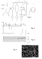
- the figure 1 is a very simplified embodiment of a magnetron-type sputtering chamber which can be used in the context of the invention, and comprising an arrangement of magnets 45, cooling channels, two sputtering targets 31 and 32, for example an aluminum target 31 and a metallic silver target 32, and voltage sources 38 capable of carrying the targets 31 and 32, as well as the desired electric potential substrate holder 35.
- the sources can be DC, RF or pulsed sources, depending on the case.
- the spraying system also includes a vacuum installation 47 and filling lines 41 making it possible to produce, within the enclosure, a controlled atmosphere of reactive or inert type. The operation of this spraying device is described in the scientific and technical literature, and it will be repeated here only in outline.
- Magnetron sputtering involves spraying a target made of a thin film deposition material.
- the target for example one of the targets 31 and 32, is negatively charged, the rest of the enclosure including the substrate holder is grounded.
- the inert gas such as argon
- the atoms of the gas will be ionized, the plasma will be created inside the enclosure.
- the presence of the magnets behind the target confines the plasma close to the target.
- the gas ions move towards the target and bombard it. This causes sputtering of the target atoms that condense on the interior walls of the enclosure, including the substrate. Spraying in a non-reactive mode (in a pure argon atmosphere) results in deposition of the target material.
- the white surface is composed of a coating comprising at least two layers 23, 24 on a substrate 21.
- the method of the invention comprises a step 220 of deposition of an underlayer 22 on the substrate 21.
- the underlayer may be for example composed of Al 2 O 3.
- the voltage V b of the substrate 21 is close to zero.
- the duration of this step can be, for example 5 ', as indicated by the figure 2 , but this is not an essential feature of the invention, the duration being higher or lower depending on the desired thickness, the power of the source and the geometry of deposition.
- Step 230 involves the manufacture of a rough layer 23, for example, a first of pure metallic aluminum and serves to create a rough surface. It is preferably done in two stages. First, a first aluminum sub-layer 23a is deposited under "normal" conditions, for example polarizing the aluminum target negatively and leaving the substrate holder 35 to ground, or at a potential close to zero, and in an inert atmosphere of Ar gas. The purpose of this deposition is to obtain an aluminum layer which will serve as a basis for further deposition. Then, the deposition of aluminum continues with the application of a negative bias on the substrate holder 35, for example -100V. In this way, an underlayer 23b is generated which has the optimum roughness necessary for the creation of a structured surface.
- a first aluminum sub-layer 23a is deposited under "normal" conditions, for example polarizing the aluminum target negatively and leaving the substrate holder 35 to ground, or at a potential close to zero, and in an inert atmosphere of Ar gas. The purpose of this deposition is to obtain an aluminum layer which
- the effect of the negative polarization of the substrate holder 35 causes a plasma formation in proximity thereto, so that the sublayer 23b is the target of a vigorous ion bombardment and is, at least in part, repulverized during the deposition.
- the roughness of the layer 23b is invisible to the naked eye and imperceptible to the touch, the average size of the asperities is preferably less than 10 microns, more preferably less than 2 microns. It has been found that these results can be obtained by depositions lasting between 1 'and 5' with a voltage of -100V at the substrate holder 35.
- the distinction between the two sublayers 23a, 23b relates solely to the spraying conditions, which differ by the application of a negative electric voltage during the deposition of the sublayer 23b.
- the two layers in this example have in fact the same chemical composition and are not necessarily distinguishable in the article of the invention.
- the first layer 23a could be omitted, or could envisage a gradual transition of the voltage of the substrate holder 35, without discontinuities between the two sub-layers.
- the second target 32 is activated, while the target 31 is deactivated, and the substrate holder 35 is brought back to a zero or zero electrical potential.
- Target 32 is preferably a target of pure silver, or other highly reflective material.
- a reflective layer 24 is then deposited on the rough layer 23. The reflective layer follows the profile of the underlying layer 23b and has a roughness comparable to that of the rough layer 23b. The outer surface of the reflective layer 24 effectively reflects the white light diffusely and non-specularly.
- the substrate 21 has a structured or decorated surface, for example a timepiece with an engraved, beaded, satin-finished, Geneva-ribbed, guilloché surface, etc.
- the decorative coating of the invention is thin enough to allow the decoration of the underlying substrate to be seen. We then obtain a surface white decorated.
- the reflective layer and the rough layer have a thickness of less than 10 ⁇ m, preferably less than 4 ⁇ m, more preferably between 1 and 3 ⁇ m.
- a colored undercoat could be deposited to obtain surfaces having a color shade.
- a non-metallic underlayer 22 for example Al2O3, improves roughness and uniformity of the rough layer.
- this underlayer could be metallic in nature, this is to improve the adhesion of the coating to the substrate.
- the layers 23, 24 could be deposited on a sub-layer 22 having one of the following compositions: Cr, Ti, Al 2 O 3, AlN, AlON, SiO 2, TiO 2, ZrO 2, DLC (diamond-like carbon).
- Aluminum and silver could also be replaced by other materials, for example layers of gold, copper, palladium, rhodium or any other material could be deposited to produce dull surfaces having a hue. It would also be possible to deposit silver-containing alloy layers 24, for example Ag-Pd, Ag-Al, Ag-Rh.
- the invention is also not limited to a spraying process, but includes any other deposition process applicable to the disclosed process.
- the invention could also provide for the deposition of additional layers, for example protective layers against tarnishing or / and transparent anti-wear layers 25.
- the protective layer could for example have one of the following inorganic compositions: Al2O3, AlN, AION, ZnO, SiO 2, TiO 2, ZrO 2, DLC (diamond-like carbon) and combinations thereof.
- the protective layer 25 could also be an organic layer painted, sprayed or applied by any suitable method.
- it could be a layer of lacquer, acrylic lacquer, nitrocellulose varnish (zapon), a polymer layer, etc.
- the reflective layer is made of silver, it will be possible to apply the methods known and normally employed to prevent tarnishing of this metal, for example chemical, galvanic or physical anti-tarnishing processes.
- the inventive method could also include steps of cleaning the substrates prior to ion pickling deposition.
- the method of the invention makes it possible to deposit a white coating on various articles in order to obtain particularly attractive decorative articles.
- a matt or glossy white coating can be deposited by the inventive method on watch elements, in particular internal trim components such as dials, hands, indexes, bridges, plates, barrels.
- the method of the invention can be applied also to other decorative items, for example jewelry or glasses frames.
Landscapes
- Chemical & Material Sciences (AREA)
- Physics & Mathematics (AREA)
- Engineering & Computer Science (AREA)
- Chemical Kinetics & Catalysis (AREA)
- Materials Engineering (AREA)
- Mechanical Engineering (AREA)
- Metallurgy (AREA)
- Organic Chemistry (AREA)
- General Physics & Mathematics (AREA)
- Optics & Photonics (AREA)
- Manufacturing & Machinery (AREA)
- Physical Vapour Deposition (AREA)
Applications Claiming Priority (1)
| Application Number | Priority Date | Filing Date | Title |
|---|---|---|---|
| CH15782010 | 2010-09-28 |
Publications (2)
| Publication Number | Publication Date |
|---|---|
| EP2434031A1 true EP2434031A1 (de) | 2012-03-28 |
| EP2434031B1 EP2434031B1 (de) | 2013-05-15 |
Family
ID=44904687
Family Applications (1)
| Application Number | Title | Priority Date | Filing Date |
|---|---|---|---|
| EP20100193388 Active EP2434031B1 (de) | 2010-09-28 | 2010-12-01 | Weiße Zierverkleidung, Dekoartikel und Verfahren |
Country Status (1)
| Country | Link |
|---|---|
| EP (1) | EP2434031B1 (de) |
Cited By (2)
| Publication number | Priority date | Publication date | Assignee | Title |
|---|---|---|---|---|
| CN103374724A (zh) * | 2012-04-12 | 2013-10-30 | 钜永真空科技股份有限公司 | 一种有色膜及其制作方法 |
| EP3220212A1 (de) * | 2016-03-16 | 2017-09-20 | The Swatch Group Research and Development Ltd. | Dekorationsverfahren für eine uhrkomponente |
Citations (7)
| Publication number | Priority date | Publication date | Assignee | Title |
|---|---|---|---|---|
| GB1460784A (en) * | 1973-06-01 | 1977-01-06 | Citizen Watch Co Ltd | Timepiece dial machine base with hydraulic controls for injection moulding machine |
| US4583866A (en) * | 1983-09-29 | 1986-04-22 | Kabushiki Kaisha Suwa Seikosha | Watch dial and method for preparation |
| US5282902A (en) * | 1991-05-09 | 1994-02-01 | Canon Kabushiki Kaisha | Solar cell provided with a light reflection layer |
| US5985469A (en) * | 1993-12-28 | 1999-11-16 | Citizen Watch Co., Ltd. | White decorative part and process for producing the same |
| EP1363143A1 (de) | 2002-05-17 | 2003-11-19 | Rolic AG | Helle und weisse optische Streuschicht |
| WO2007081484A1 (en) | 2006-01-04 | 2007-07-19 | Guardian Industries Corp. | Optical diffuser having frit based coating with inorganic light diffusing pigments with variable particle size therein |
| US20090176121A1 (en) * | 2008-01-08 | 2009-07-09 | Kabushiki Kaisha Kobe Seiko Sho (Kobe Steel, Ltd.) | Electroconductive diffuse reflective film and method of producing the same |
-
2010
- 2010-12-01 EP EP20100193388 patent/EP2434031B1/de active Active
Patent Citations (7)
| Publication number | Priority date | Publication date | Assignee | Title |
|---|---|---|---|---|
| GB1460784A (en) * | 1973-06-01 | 1977-01-06 | Citizen Watch Co Ltd | Timepiece dial machine base with hydraulic controls for injection moulding machine |
| US4583866A (en) * | 1983-09-29 | 1986-04-22 | Kabushiki Kaisha Suwa Seikosha | Watch dial and method for preparation |
| US5282902A (en) * | 1991-05-09 | 1994-02-01 | Canon Kabushiki Kaisha | Solar cell provided with a light reflection layer |
| US5985469A (en) * | 1993-12-28 | 1999-11-16 | Citizen Watch Co., Ltd. | White decorative part and process for producing the same |
| EP1363143A1 (de) | 2002-05-17 | 2003-11-19 | Rolic AG | Helle und weisse optische Streuschicht |
| WO2007081484A1 (en) | 2006-01-04 | 2007-07-19 | Guardian Industries Corp. | Optical diffuser having frit based coating with inorganic light diffusing pigments with variable particle size therein |
| US20090176121A1 (en) * | 2008-01-08 | 2009-07-09 | Kabushiki Kaisha Kobe Seiko Sho (Kobe Steel, Ltd.) | Electroconductive diffuse reflective film and method of producing the same |
Cited By (6)
| Publication number | Priority date | Publication date | Assignee | Title |
|---|---|---|---|---|
| CN103374724A (zh) * | 2012-04-12 | 2013-10-30 | 钜永真空科技股份有限公司 | 一种有色膜及其制作方法 |
| EP3220212A1 (de) * | 2016-03-16 | 2017-09-20 | The Swatch Group Research and Development Ltd. | Dekorationsverfahren für eine uhrkomponente |
| US20170268111A1 (en) * | 2016-03-16 | 2017-09-21 | The Swatch Group Research And Development Ltd | Method for decorating a timepiece component |
| JP2017167138A (ja) * | 2016-03-16 | 2017-09-21 | ザ・スウォッチ・グループ・リサーチ・アンド・ディベロップメント・リミテッド | 計時器用部品を装飾する方法 |
| CN107203122A (zh) * | 2016-03-16 | 2017-09-26 | 斯沃奇集团研究和开发有限公司 | 装饰钟表部件的方法 |
| US11208715B2 (en) | 2016-03-16 | 2021-12-28 | The Swatch Group Research And Development Ltd | Method for decorating a timepiece component |
Also Published As
| Publication number | Publication date |
|---|---|
| EP2434031B1 (de) | 2013-05-15 |
Similar Documents
| Publication | Publication Date | Title |
|---|---|---|
| EP0258283B1 (de) | Verfahren zum beschichten eines substrates mit einem verschleissfesten, dekorativen überzug und ein gemäss diesem verfahren hergestellter artikel | |
| Constantin et al. | Performance of hard coatings, made by balanced and unbalanced magnetron sputtering, for decorative applications | |
| FR2572421A1 (fr) | Procede pour appliquer un revetement de microcouches de deux matieres alternees, et objets revetus obtenus | |
| JP5930783B2 (ja) | 有色硬質装飾部材 | |
| US20130164472A1 (en) | Housing and method for making the same | |
| US20120121856A1 (en) | Coated article and method for making same | |
| EP2392689B1 (de) | Dekorationsartikel mit roter Beschichtung, und Verfahren | |
| CH711122A2 (fr) | Revêtement protecteur, décoratif blanc, et procédé de déposition. | |
| CH709669A1 (fr) | Couche protectrice, décorative et procédé de déposition. | |
| EP2434031B1 (de) | Weiße Zierverkleidung, Dekoartikel und Verfahren | |
| EP3835452A1 (de) | Herstellungsverfahren einer dekoroberfläche | |
| TWI448385B (zh) | 有色膜結構作為增加產品外觀之用途與用於增加產品外觀之有色膜結構之製造方法 | |
| CN106637128A (zh) | 金及其合金表面透明类金刚石纳米薄膜及其制备方法 | |
| FR2943072B1 (fr) | Decoration par pulverisation plasma magnetron sur des contenants en verre pour les secteurs de la cosmetique. | |
| WO2022033741A1 (fr) | Composant noir et son procede de fabrication | |
| Shankernath et al. | Optical response of ultra-thin titanium nitride films on brass and gold plated brass surfaces | |
| FR2843130A1 (fr) | Procede de revetement de la surface d'un materiau metallique, dispositif pour sa mise en oeuvre et produit ainsi obtenu | |
| EP4060386A1 (de) | Verkleidungsteil einer uhr oder eines schmuckstücks mit einer interferenzfarbbeschichtung und verfahren zur herstellung dieses teils | |
| Yate et al. | Control of the bias voltage in dc PVD processes on insulator substrates | |
| CN113151794A (zh) | 一种镁合金表面增硬耐磨防腐彩色涂层及其制备工艺 | |
| EP1614764B1 (de) | Dekorative Beschichtung durch die Abscheidung von abwechselnden Nitridschichten | |
| Frach et al. | Advanced key technologies for magnetron sputtering and PECVD of inorganic and hybrid transparent coatings | |
| CH717875A2 (fr) | Composant noir et son procédé de fabrication. | |
| JP2010072347A (ja) | 光学干渉薄膜 | |
| EP4344576A1 (de) | Verfahren zur herstellung eines verkleidungsbauteils mit einer schutzschicht |
Legal Events
| Date | Code | Title | Description |
|---|---|---|---|
| PUAI | Public reference made under article 153(3) epc to a published international application that has entered the european phase |
Free format text: ORIGINAL CODE: 0009012 |
|
| AK | Designated contracting states |
Kind code of ref document: A1 Designated state(s): AL AT BE BG CH CY CZ DE DK EE ES FI FR GB GR HR HU IE IS IT LI LT LU LV MC MK MT NL NO PL PT RO RS SE SI SK SM TR |
|
| AX | Request for extension of the european patent |
Extension state: BA ME |
|
| 17P | Request for examination filed |
Effective date: 20120707 |
|
| 17Q | First examination report despatched |
Effective date: 20120928 |
|
| GRAP | Despatch of communication of intention to grant a patent |
Free format text: ORIGINAL CODE: EPIDOSNIGR1 |
|
| GRAS | Grant fee paid |
Free format text: ORIGINAL CODE: EPIDOSNIGR3 |
|
| GRAA | (expected) grant |
Free format text: ORIGINAL CODE: 0009210 |
|
| AK | Designated contracting states |
Kind code of ref document: B1 Designated state(s): AL AT BE BG CH CY CZ DE DK EE ES FI FR GB GR HR HU IE IS IT LI LT LU LV MC MK MT NL NO PL PT RO RS SE SI SK SM TR |
|
| REG | Reference to a national code |
Ref country code: GB Ref legal event code: FG4D Free format text: NOT ENGLISH Ref country code: CH Ref legal event code: EP |
|
| REG | Reference to a national code |
Ref country code: AT Ref legal event code: REF Ref document number: 612202 Country of ref document: AT Kind code of ref document: T Effective date: 20130615 |
|
| REG | Reference to a national code |
Ref country code: IE Ref legal event code: FG4D Free format text: LANGUAGE OF EP DOCUMENT: FRENCH |
|
| REG | Reference to a national code |
Ref country code: DE Ref legal event code: R096 Ref document number: 602010007074 Country of ref document: DE Effective date: 20130711 |
|
| REG | Reference to a national code |
Ref country code: AT Ref legal event code: MK05 Ref document number: 612202 Country of ref document: AT Kind code of ref document: T Effective date: 20130515 |
|
| REG | Reference to a national code |
Ref country code: LT Ref legal event code: MG4D |
|
| REG | Reference to a national code |
Ref country code: NL Ref legal event code: VDEP Effective date: 20130515 Ref country code: DE Ref legal event code: R082 Ref document number: 602010007074 Country of ref document: DE Representative=s name: WOHLMUTH, JOHANNES, DIPL.-PHYS., CH |
|
| PG25 | Lapsed in a contracting state [announced via postgrant information from national office to epo] |
Ref country code: IS Free format text: LAPSE BECAUSE OF FAILURE TO SUBMIT A TRANSLATION OF THE DESCRIPTION OR TO PAY THE FEE WITHIN THE PRESCRIBED TIME-LIMIT Effective date: 20130915 Ref country code: GR Free format text: LAPSE BECAUSE OF FAILURE TO SUBMIT A TRANSLATION OF THE DESCRIPTION OR TO PAY THE FEE WITHIN THE PRESCRIBED TIME-LIMIT Effective date: 20130816 Ref country code: ES Free format text: LAPSE BECAUSE OF FAILURE TO SUBMIT A TRANSLATION OF THE DESCRIPTION OR TO PAY THE FEE WITHIN THE PRESCRIBED TIME-LIMIT Effective date: 20130826 Ref country code: PT Free format text: LAPSE BECAUSE OF FAILURE TO SUBMIT A TRANSLATION OF THE DESCRIPTION OR TO PAY THE FEE WITHIN THE PRESCRIBED TIME-LIMIT Effective date: 20130916 Ref country code: AT Free format text: LAPSE BECAUSE OF FAILURE TO SUBMIT A TRANSLATION OF THE DESCRIPTION OR TO PAY THE FEE WITHIN THE PRESCRIBED TIME-LIMIT Effective date: 20130515 Ref country code: SE Free format text: LAPSE BECAUSE OF FAILURE TO SUBMIT A TRANSLATION OF THE DESCRIPTION OR TO PAY THE FEE WITHIN THE PRESCRIBED TIME-LIMIT Effective date: 20130515 Ref country code: NO Free format text: LAPSE BECAUSE OF FAILURE TO SUBMIT A TRANSLATION OF THE DESCRIPTION OR TO PAY THE FEE WITHIN THE PRESCRIBED TIME-LIMIT Effective date: 20130815 Ref country code: SI Free format text: LAPSE BECAUSE OF FAILURE TO SUBMIT A TRANSLATION OF THE DESCRIPTION OR TO PAY THE FEE WITHIN THE PRESCRIBED TIME-LIMIT Effective date: 20130515 Ref country code: LT Free format text: LAPSE BECAUSE OF FAILURE TO SUBMIT A TRANSLATION OF THE DESCRIPTION OR TO PAY THE FEE WITHIN THE PRESCRIBED TIME-LIMIT Effective date: 20130515 Ref country code: FI Free format text: LAPSE BECAUSE OF FAILURE TO SUBMIT A TRANSLATION OF THE DESCRIPTION OR TO PAY THE FEE WITHIN THE PRESCRIBED TIME-LIMIT Effective date: 20130515 |
|
| REG | Reference to a national code |
Ref country code: CH Ref legal event code: PUE Owner name: L.A.C. SARL, LABORATORY FOR ADVANCED COATINGS, CH Free format text: FORMER OWNER: HAUTE ECOLE ARC, CH Ref country code: CH Ref legal event code: NV Representative=s name: P&TS SA, CH |
|
| RAP2 | Party data changed (patent owner data changed or rights of a patent transferred) |
Owner name: L.A.C. SARL |
|
| PG25 | Lapsed in a contracting state [announced via postgrant information from national office to epo] |
Ref country code: RS Free format text: LAPSE BECAUSE OF FAILURE TO SUBMIT A TRANSLATION OF THE DESCRIPTION OR TO PAY THE FEE WITHIN THE PRESCRIBED TIME-LIMIT Effective date: 20130515 Ref country code: PL Free format text: LAPSE BECAUSE OF FAILURE TO SUBMIT A TRANSLATION OF THE DESCRIPTION OR TO PAY THE FEE WITHIN THE PRESCRIBED TIME-LIMIT Effective date: 20130515 Ref country code: BG Free format text: LAPSE BECAUSE OF FAILURE TO SUBMIT A TRANSLATION OF THE DESCRIPTION OR TO PAY THE FEE WITHIN THE PRESCRIBED TIME-LIMIT Effective date: 20130815 Ref country code: HR Free format text: LAPSE BECAUSE OF FAILURE TO SUBMIT A TRANSLATION OF THE DESCRIPTION OR TO PAY THE FEE WITHIN THE PRESCRIBED TIME-LIMIT Effective date: 20130515 |
|
| REG | Reference to a national code |
Ref country code: DE Ref legal event code: R082 Ref document number: 602010007074 Country of ref document: DE Representative=s name: WOHLMUTH, JOHANNES, DIPL.-PHYS., CH Effective date: 20131030 Ref country code: DE Ref legal event code: R082 Ref document number: 602010007074 Country of ref document: DE Representative=s name: WOHLMUTH, JOHANNES, DIPL.-PHYS., DE Effective date: 20131030 Ref country code: DE Ref legal event code: R081 Ref document number: 602010007074 Country of ref document: DE Owner name: L.A.C. SARL, CH Free format text: FORMER OWNER: HAUTE ECOLE ARC, ST.-IMIER, CH Effective date: 20131030 |
|
| PG25 | Lapsed in a contracting state [announced via postgrant information from national office to epo] |
Ref country code: LV Free format text: LAPSE BECAUSE OF FAILURE TO SUBMIT A TRANSLATION OF THE DESCRIPTION OR TO PAY THE FEE WITHIN THE PRESCRIBED TIME-LIMIT Effective date: 20130515 |
|
| PG25 | Lapsed in a contracting state [announced via postgrant information from national office to epo] |
Ref country code: CZ Free format text: LAPSE BECAUSE OF FAILURE TO SUBMIT A TRANSLATION OF THE DESCRIPTION OR TO PAY THE FEE WITHIN THE PRESCRIBED TIME-LIMIT Effective date: 20130515 Ref country code: DK Free format text: LAPSE BECAUSE OF FAILURE TO SUBMIT A TRANSLATION OF THE DESCRIPTION OR TO PAY THE FEE WITHIN THE PRESCRIBED TIME-LIMIT Effective date: 20130515 Ref country code: SK Free format text: LAPSE BECAUSE OF FAILURE TO SUBMIT A TRANSLATION OF THE DESCRIPTION OR TO PAY THE FEE WITHIN THE PRESCRIBED TIME-LIMIT Effective date: 20130515 Ref country code: EE Free format text: LAPSE BECAUSE OF FAILURE TO SUBMIT A TRANSLATION OF THE DESCRIPTION OR TO PAY THE FEE WITHIN THE PRESCRIBED TIME-LIMIT Effective date: 20130515 |
|
| PG25 | Lapsed in a contracting state [announced via postgrant information from national office to epo] |
Ref country code: RO Free format text: LAPSE BECAUSE OF FAILURE TO SUBMIT A TRANSLATION OF THE DESCRIPTION OR TO PAY THE FEE WITHIN THE PRESCRIBED TIME-LIMIT Effective date: 20130515 Ref country code: NL Free format text: LAPSE BECAUSE OF FAILURE TO SUBMIT A TRANSLATION OF THE DESCRIPTION OR TO PAY THE FEE WITHIN THE PRESCRIBED TIME-LIMIT Effective date: 20130515 |
|
| PLBE | No opposition filed within time limit |
Free format text: ORIGINAL CODE: 0009261 |
|
| STAA | Information on the status of an ep patent application or granted ep patent |
Free format text: STATUS: NO OPPOSITION FILED WITHIN TIME LIMIT |
|
| 26N | No opposition filed |
Effective date: 20140218 |
|
| REG | Reference to a national code |
Ref country code: DE Ref legal event code: R097 Ref document number: 602010007074 Country of ref document: DE Effective date: 20140218 |
|
| BERE | Be: lapsed |
Owner name: HAUTE ECOLE ARC Effective date: 20131231 |
|
| PG25 | Lapsed in a contracting state [announced via postgrant information from national office to epo] |
Ref country code: LU Free format text: LAPSE BECAUSE OF FAILURE TO SUBMIT A TRANSLATION OF THE DESCRIPTION OR TO PAY THE FEE WITHIN THE PRESCRIBED TIME-LIMIT Effective date: 20131201 |
|
| REG | Reference to a national code |
Ref country code: IE Ref legal event code: MM4A |
|
| PG25 | Lapsed in a contracting state [announced via postgrant information from national office to epo] |
Ref country code: BE Free format text: LAPSE BECAUSE OF NON-PAYMENT OF DUE FEES Effective date: 20131231 Ref country code: IE Free format text: LAPSE BECAUSE OF NON-PAYMENT OF DUE FEES Effective date: 20131201 |
|
| PG25 | Lapsed in a contracting state [announced via postgrant information from national office to epo] |
Ref country code: MC Free format text: LAPSE BECAUSE OF FAILURE TO SUBMIT A TRANSLATION OF THE DESCRIPTION OR TO PAY THE FEE WITHIN THE PRESCRIBED TIME-LIMIT Effective date: 20130515 |
|
| PG25 | Lapsed in a contracting state [announced via postgrant information from national office to epo] |
Ref country code: SM Free format text: LAPSE BECAUSE OF FAILURE TO SUBMIT A TRANSLATION OF THE DESCRIPTION OR TO PAY THE FEE WITHIN THE PRESCRIBED TIME-LIMIT Effective date: 20130515 |
|
| PG25 | Lapsed in a contracting state [announced via postgrant information from national office to epo] |
Ref country code: TR Free format text: LAPSE BECAUSE OF FAILURE TO SUBMIT A TRANSLATION OF THE DESCRIPTION OR TO PAY THE FEE WITHIN THE PRESCRIBED TIME-LIMIT Effective date: 20130515 Ref country code: CY Free format text: LAPSE BECAUSE OF FAILURE TO SUBMIT A TRANSLATION OF THE DESCRIPTION OR TO PAY THE FEE WITHIN THE PRESCRIBED TIME-LIMIT Effective date: 20130515 |
|
| PG25 | Lapsed in a contracting state [announced via postgrant information from national office to epo] |
Ref country code: MK Free format text: LAPSE BECAUSE OF FAILURE TO SUBMIT A TRANSLATION OF THE DESCRIPTION OR TO PAY THE FEE WITHIN THE PRESCRIBED TIME-LIMIT Effective date: 20130515 Ref country code: HU Free format text: LAPSE BECAUSE OF FAILURE TO SUBMIT A TRANSLATION OF THE DESCRIPTION OR TO PAY THE FEE WITHIN THE PRESCRIBED TIME-LIMIT; INVALID AB INITIO Effective date: 20101201 |
|
| GBPC | Gb: european patent ceased through non-payment of renewal fee |
Effective date: 20141201 |
|
| PG25 | Lapsed in a contracting state [announced via postgrant information from national office to epo] |
Ref country code: MT Free format text: LAPSE BECAUSE OF FAILURE TO SUBMIT A TRANSLATION OF THE DESCRIPTION OR TO PAY THE FEE WITHIN THE PRESCRIBED TIME-LIMIT Effective date: 20130515 |
|
| PG25 | Lapsed in a contracting state [announced via postgrant information from national office to epo] |
Ref country code: GB Free format text: LAPSE BECAUSE OF NON-PAYMENT OF DUE FEES Effective date: 20141201 |
|
| REG | Reference to a national code |
Ref country code: FR Ref legal event code: PLFP Year of fee payment: 6 |
|
| REG | Reference to a national code |
Ref country code: DE Ref legal event code: R082 Ref document number: 602010007074 Country of ref document: DE Representative=s name: BECK & ROESSIG - EUROPEAN PATENT ATTORNEYS, DE Ref country code: DE Ref legal event code: R082 Ref document number: 602010007074 Country of ref document: DE Representative=s name: WOHLMUTH, JOHANNES, DIPL.-PHYS., DE |
|
| REG | Reference to a national code |
Ref country code: FR Ref legal event code: PLFP Year of fee payment: 7 |
|
| REG | Reference to a national code |
Ref country code: FR Ref legal event code: PLFP Year of fee payment: 8 |
|
| PG25 | Lapsed in a contracting state [announced via postgrant information from national office to epo] |
Ref country code: AL Free format text: LAPSE BECAUSE OF FAILURE TO SUBMIT A TRANSLATION OF THE DESCRIPTION OR TO PAY THE FEE WITHIN THE PRESCRIBED TIME-LIMIT Effective date: 20130515 |
|
| REG | Reference to a national code |
Ref country code: DE Ref legal event code: R082 Ref document number: 602010007074 Country of ref document: DE Representative=s name: BECK & ROESSIG - EUROPEAN PATENT ATTORNEYS, DE |
|
| PGFP | Annual fee paid to national office [announced via postgrant information from national office to epo] |
Ref country code: DE Payment date: 20211210 Year of fee payment: 12 |
|
| PGFP | Annual fee paid to national office [announced via postgrant information from national office to epo] |
Ref country code: IT Payment date: 20211224 Year of fee payment: 12 |
|
| PGFP | Annual fee paid to national office [announced via postgrant information from national office to epo] |
Ref country code: FR Payment date: 20221222 Year of fee payment: 13 |
|
| REG | Reference to a national code |
Ref country code: DE Ref legal event code: R119 Ref document number: 602010007074 Country of ref document: DE |
|
| PG25 | Lapsed in a contracting state [announced via postgrant information from national office to epo] |
Ref country code: DE Free format text: LAPSE BECAUSE OF NON-PAYMENT OF DUE FEES Effective date: 20230701 |
|
| PG25 | Lapsed in a contracting state [announced via postgrant information from national office to epo] |
Ref country code: IT Free format text: LAPSE BECAUSE OF NON-PAYMENT OF DUE FEES Effective date: 20221201 |
|
| PGFP | Annual fee paid to national office [announced via postgrant information from national office to epo] |
Ref country code: CH Payment date: 20240307 Year of fee payment: 14 |