EP2433296B1 - Semiconductor device contacts - Google Patents
Semiconductor device contacts Download PDFInfo
- Publication number
- EP2433296B1 EP2433296B1 EP10725837.8A EP10725837A EP2433296B1 EP 2433296 B1 EP2433296 B1 EP 2433296B1 EP 10725837 A EP10725837 A EP 10725837A EP 2433296 B1 EP2433296 B1 EP 2433296B1
- Authority
- EP
- European Patent Office
- Prior art keywords
- contact
- semiconductor
- accordance
- oxide
- contact material
- Prior art date
- Legal status (The legal status is an assumption and is not a legal conclusion. Google has not performed a legal analysis and makes no representation as to the accuracy of the status listed.)
- Active
Links
Images

Classifications
-
- H—ELECTRICITY
- H10—SEMICONDUCTOR DEVICES; ELECTRIC SOLID-STATE DEVICES NOT OTHERWISE PROVIDED FOR
- H10D—INORGANIC ELECTRIC SEMICONDUCTOR DEVICES
- H10D62/00—Semiconductor bodies, or regions thereof, of devices having potential barriers
- H10D62/80—Semiconductor bodies, or regions thereof, of devices having potential barriers characterised by the materials
- H10D62/86—Semiconductor bodies, or regions thereof, of devices having potential barriers characterised by the materials being Group II-VI materials, e.g. ZnO
- H10D62/8603—Binary Group II-VI materials wherein cadmium is the Group II element, e.g. CdTe
-
- H—ELECTRICITY
- H10—SEMICONDUCTOR DEVICES; ELECTRIC SOLID-STATE DEVICES NOT OTHERWISE PROVIDED FOR
- H10D—INORGANIC ELECTRIC SEMICONDUCTOR DEVICES
- H10D64/00—Electrodes of devices having potential barriers
- H10D64/60—Electrodes characterised by their materials
- H10D64/62—Electrodes ohmically coupled to a semiconductor
Definitions
- the invention relates to a method of fabrication of electrical contact structures for a semiconductor and to a method of fabrication of a semiconductor device incorporating such electrical contact structures.
- the invention in particular relates to the fabrication of a semiconductor device for high energy physics applications, such as a detector for high energy radiation.
- the invention in particular relates to the fabrication of a semiconductor device comprising a large direct band gap semiconductor material, for example a group II-VI semiconductor material such as cadmium telluride (CdTe), cadmium zinc telluride (CZT), cadmium manganese telluride (CMT) or the like, for example formed as a bulk single crystal.
- a group II-VI semiconductor material such as cadmium telluride (CdTe), cadmium zinc telluride (CZT), cadmium manganese telluride (CMT) or the like, for example formed as a bulk single crystal.
- Cadmium telluride and similar semiconductor materials have found application in recent years in a variety of high energy physics applications, such high energy radiation detection. In particular their ability to resolve high energy electromagnetic radiation such as x-rays or gamma rays spectroscopically has been utilised. This may be especially the case where the material is fabricated as a bulk scale single crystal, which has become a more practical proposition as a result of the development of bulk vapour deposition techniques, for example multi-tube physical vapour phase transport methods, such as that disclosed in EP-B-1019568 .
- the performance of the devices based on such materials depends both on the electrical properties of the semiconductor and on the qualities of the deposited contacts and more precisely on the interface formed between contact/semiconductor.
- the contact material can inherently affect the overall device behaviour, as can the choice of the deposition method since this can have an important influence on the composition of the interfacial layer formed between contact/ semiconductor.
- Current practical methods for deposition of contacts include evaporation, sputtering, electrolytic and electroless chemical deposition.
- the deposition of contact done by a physical deposition method is following by an annealing process to diffuse the metal in the CdTe and, like this, to have a good contact between the two elements.
- Deposition by a chemical electroless process is often preferred as a method simpler and quicker to carry out than the physical deposition and as a method that creates a stronger chemical bonding between the contacts and the material CdTe without necessity to anneal.
- three standard types of contacts, gold, platinum and palladium contacts, are typically produced by this method. The range of practical chemical electroless contacts is thus generally limited.
- US Patent No 5731634 describes a method of forming a metal oxide film on an insulating film formed on a semiconductor substrate.
- a method of fabrication of contacts on a semiconductor material comprises the steps of:
- the method is characterised in that the step of depositing an oxide of a desired contact material by a chemical electroless process on a face of the semiconductor material comprises applying a deposition solution selected such that a relatively insoluble oxide of a desired contact material is deposited onto the face of the semiconductor material in that the relatively insoluble oxide is formed chemically at the semiconductor surface by oxidation of the semiconductor material at the surface.
- a method of fabrication of a semiconductor device comprises:
- Deposition is via a two-stage chemical electroless process.
- the use of the chemical electroless method may present a number of advantages in comparison with the other methods of deposition such as evaporation, sputtering; including one or more of:
- the two stage process is found to increase significantly the range of contact materials available for use.
- Contact materials must comprise suitable electrical conductors in the reduced state. Subject to this proviso they may be metal or non-metallic semiconductor, pure element or alloy.
- the step of depositing an oxide of a desired contact material by a chemical electroless process on a face of the semiconductor material conveniently comprises applying to the semiconductor, and in particular immersing the semiconductor in, a solution from which a relatively insoluble oxide of a desired contact material is deposited onto the semiconductor material.
- a solution thus comprises a deposition solution.
- the relatively insoluble oxide layer is formed chemically at the semiconductor surface by oxidation of the semiconductor material at the surface.
- the step of depositing an oxide of a desired contact material is performed in an acidic environment, for example by applying to and for example immersing in an acidic solution.
- the deposition solution is acidic.
- the solution includes oxoacid anions of the desired contact material.
- the deposition solution comprises a solution of a metal oxoacid of a desired metal contact material.
- the step of reducing the resultant oxide via a chemical electroless process to produce a contact of the desired contact material conveniently comprises applying to the semiconductor, and in particular immersing the semiconductor in, a reducing agent.
- the step of depositing an oxide of a desired contact material is performed in a basic environment, for example by applying to and for example immersing in a basic solution.
- a convenient reducing agent might include ammonia solution.
- the method comprises dipping the semiconductor successively into a first, deposition solution by means of which an oxide layer is formed via a chemical electroless process and for example oxidatively at the semiconductor surface and into a second, reducing solution by means of which the oxide layer is reduced via a chemical electroless process to a layer of desired contact material.
- the semiconductor material onto which the contact is deposited is preferably a material adapted for high energy physics applications, such as a material able to act as a detector for high energy radiation, and for example high energy electromagnetic radiation such as x-rays or gamma rays or subatomic particle radiation.
- the resultant device comprises at least one layer of such material and is thus a device adapted for high energy physics applications, and a detector for high energy radiation such as x-rays or gamma rays or subatomic particle radiation.
- the semiconductor device is a detector device adapted to exhibit a spectroscopically variable response to incident radiation across at least a substantial part of the radiation spectrum in use.
- the semiconductor material preferably exhibits inherently as a direct material property a direct variable electrical and for example photoelectric response to different parts of the radiation spectrum in use.
- the semiconductor material is formed as a bulk crystal, and for example as a bulk single crystal (where bulk crystal in this context indicates a thickness of at least 500 ⁇ m, and preferably of at least 1 mm).
- the semiconductor material may be selected from Group II-VI semiconductors and in particular may be selected from cadmium telluride, cadmium zinc telluride (CZT), cadmium manganese telluride (CMT), and alloys thereof, and for example comprise crystalline Cd 1-(a+b) Mn a Zn b Te where a+b ⁇ 1 and a and/ or b may be zero.
- contacts for such materials applied by a chemical electroless process have typically been limited to the three standard types of contacts, gold, platinum and palladium.
- the method of the invention makes a greater range of contact materials more practical.
- the invention makes it possible to select as a contact material a material to form an ohmic contact, for example a material having a high work function offering potentially better ohmic behaviour than Au, Pt or Pd.
- a contact material for example a material having a high work function offering potentially better ohmic behaviour than Au, Pt or Pd.
- examples of such materials include materials selected from the group comprising Ge, W, Mo, Cu, Ir, Rh, Ru, Se, Sn, Os, Re, Ni, Sb and alloys and combinations thereof.
- the invention makes it possible to select as a contact material a material to form a Schottky diode/ blocking contact. Examples of such materials include include materials selected from the group comprising Bi, In, Tl and alloys and combinations thereof.
- Transition metals and in particular those with a larger number of valence electrons may be preferred.
- Metals which form oxoanions soluble in aqueous acid conditions with a valency of at least five, and more preferably at least six, which are capable of being reduced by electroless reaction with the surface of the semiconductor material to form a stable relatively insoluble oxide layer may be preferred.
- Tungsten and molybdenum are particularly suited to the method of the invention.
- W and Mo are particularly interesting elements because both have a higher work function than CdTe and a rich number of valence electrons.
- the tungsten contacts are carried out by dipping the CdTe into two baths.
- the first bath comprises an acid solution from which insoluble oxides of tungsten may be deposited at the CdTe semiconductor surface.
- the second bath reduces these oxides to tungsten metal.
- the first bath has the purpose to create a strong chemical bonding between CdTe and W through a layer of tungsten oxide.
- This bath is a mixture of tungstic acid (H 2 WO 4 ) in main component.
- the tungsten compound is under the form WO 4 2- ions in the solution.
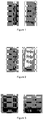
- the detector After a few seconds of dipping, the detector is covered with a brown layer (WO 2 ) with blue reflections (W 2 O 5 ) like shown on the Fig 1 .
- WO 2 brown layer
- W 2 O 5 blue reflections
- the second bath is an ammonia solution; it has the purpose to reduce the oxide layers to tungsten metal: W 2 O 5 (s) ⁇ WO 2 (s) ⁇ W(s) After few minutes of dipping, the coating of oxides is reduced in tungsten as shown on the Fig 2 .
- molybdenum contacts are created by dipping CdTe semiconductor material into two baths.
- the first bath creates an oxide layer at the surface of CdTe.
- This bath is a mixture of molybdic acid (H 2 MoO 4 ) mainly.
- the ions HMoO 4 - and MoO 4 2- are in the majority in the solution.
- the choice of reactants (other than molybdic acid) in the solution is critical to stabilize one or two forms of oxides. After few minutes of dipping, the detector is covered with a gray layer.
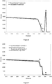
- Detector characterisation data is shown in figure 4 and 5 and in the tables below for tungsten and molybdenum and platinum contacts.
- Table 1 - Data for figures 4 and 5 example Size (mm) Voltage (V) I (nA) P/V FWHM (KeV) Efficiency Pt/Pt contact 4x4x2 100 70 3.5 8.1 202 Mo/Mo contact 4x4x2 100 90 3.5 8.2 206 W/W contact 4x4x2 100 100 2.4 14 198
- tungsten and molybdenum are described as suitable preferred example contacts and CdTe as a suitable preferred example semiconductor, but that the principles of the two stage electroless contact deposition described in accordance with the invention may be appropriate to a range of semiconductor materials and to the deposition of other contact materials exhibiting similar chemistry.
Landscapes
- Electrodes Of Semiconductors (AREA)
- Light Receiving Elements (AREA)
- Internal Circuitry In Semiconductor Integrated Circuit Devices (AREA)
Description
- The invention relates to a method of fabrication of electrical contact structures for a semiconductor and to a method of fabrication of a semiconductor device incorporating such electrical contact structures.
- The invention in particular relates to the fabrication of a semiconductor device for high energy physics applications, such as a detector for high energy radiation.
- The invention in particular relates to the fabrication of a semiconductor device comprising a large direct band gap semiconductor material, for example a group II-VI semiconductor material such as cadmium telluride (CdTe), cadmium zinc telluride (CZT), cadmium manganese telluride (CMT) or the like, for example formed as a bulk single crystal.
- Cadmium telluride and similar semiconductor materials have found application in recent years in a variety of high energy physics applications, such high energy radiation detection. In particular their ability to resolve high energy electromagnetic radiation such as x-rays or gamma rays spectroscopically has been utilised. This may be especially the case where the material is fabricated as a bulk scale single crystal, which has become a more practical proposition as a result of the development of bulk vapour deposition techniques, for example multi-tube physical vapour phase transport methods, such as that disclosed in
EP-B-1019568 . - The performance of the devices based on such materials depends both on the electrical properties of the semiconductor and on the qualities of the deposited contacts and more precisely on the interface formed between contact/semiconductor. Indeed, the contact material can inherently affect the overall device behaviour, as can the choice of the deposition method since this can have an important influence on the composition of the interfacial layer formed between contact/ semiconductor. Current practical methods for deposition of contacts include evaporation, sputtering, electrolytic and electroless chemical deposition.
- To make a good nuclear detector in CdTe, it is important to have two types of contacts: one is injecting type on one face of the detector and the other is blocking type on the other face. The choice of an optimized couple injecting/blocking assures to limit the leakage current and allows the application of a high voltage into the device, without having a polarisation effect.
- At the present time, the deposition of contact done by a physical deposition method (e.g. sputtering) is following by an annealing process to diffuse the metal in the CdTe and, like this, to have a good contact between the two elements.
- Deposition by a chemical electroless process is often preferred as a method simpler and quicker to carry out than the physical deposition and as a method that creates a stronger chemical bonding between the contacts and the material CdTe without necessity to anneal. At the present time three standard types of contacts, gold, platinum and palladium contacts, are typically produced by this method. The range of practical chemical electroless contacts is thus generally limited.
-
US Patent No 5731634 describes a method of forming a metal oxide film on an insulating film formed on a semiconductor substrate. - According to the invention in a first aspect a method of fabrication of contacts on a semiconductor material comprises the steps of:
- depositing an oxide of a desired contact material by a chemical electroless process on a face of the semiconductor material; and
- reducing the oxide via a chemical electroless process to produce a contact of the desired material.
- The method is characterised in that the step of depositing an oxide of a desired contact material by a chemical electroless process on a face of the semiconductor material comprises applying a deposition solution selected such that a relatively insoluble oxide of a desired contact material is deposited onto the face of the semiconductor material in that the relatively insoluble oxide is formed chemically at the semiconductor surface by oxidation of the semiconductor material at the surface.
- According to the invention in a further aspect, a method of fabrication of a semiconductor device comprises:
- providing a semiconductor structure having at least a first layer of semiconductor material on which it is desired to create an electrical contact;
- and fabricating a contact thereon via the method of the first aspect.
- Deposition is via a two-stage chemical electroless process. The use of the chemical electroless method may present a number of advantages in comparison with the other methods of deposition such as evaporation, sputtering; including one or more of:
- Easy and fast deposition (few minutes).
- Avoids sources of contamination and reduces the formation of oxide layers before contact deposition.
- Allows the deposition of injecting contacts, which are able to solve the problem of polarisation.
- Low cost.
- The two stage process is found to increase significantly the range of contact materials available for use. In particular, it may become possible to deposit contact materials having a work function substantially different from the semiconductor material and of Au, Pt or Pd. Contact materials must comprise suitable electrical conductors in the reduced state. Subject to this proviso they may be metal or non-metallic semiconductor, pure element or alloy.
- The step of depositing an oxide of a desired contact material by a chemical electroless process on a face of the semiconductor material conveniently comprises applying to the semiconductor, and in particular immersing the semiconductor in, a solution from which a relatively insoluble oxide of a desired contact material is deposited onto the semiconductor material. Such a solution thus comprises a deposition solution. The relatively insoluble oxide layer is formed chemically at the semiconductor surface by oxidation of the semiconductor material at the surface. Preferably the step of depositing an oxide of a desired contact material is performed in an acidic environment, for example by applying to and for example immersing in an acidic solution. Preferably the deposition solution is acidic. Particularly preferably the solution includes oxoacid anions of the desired contact material. For example the deposition solution comprises a solution of a metal oxoacid of a desired metal contact material.
- The step of reducing the resultant oxide via a chemical electroless process to produce a contact of the desired contact material conveniently comprises applying to the semiconductor, and in particular immersing the semiconductor in, a reducing agent. Preferably the step of depositing an oxide of a desired contact material is performed in a basic environment, for example by applying to and for example immersing in a basic solution.
- A convenient reducing agent might include ammonia solution.
- Thus in the preferred case the method comprises dipping the semiconductor successively into a first, deposition solution by means of which an oxide layer is formed via a chemical electroless process and for example oxidatively at the semiconductor surface and into a second, reducing solution by means of which the oxide layer is reduced via a chemical electroless process to a layer of desired contact material.
- The semiconductor material onto which the contact is deposited is preferably a material adapted for high energy physics applications, such as a material able to act as a detector for high energy radiation, and for example high energy electromagnetic radiation such as x-rays or gamma rays or subatomic particle radiation. The resultant device comprises at least one layer of such material and is thus a device adapted for high energy physics applications, and a detector for high energy radiation such as x-rays or gamma rays or subatomic particle radiation.
- In an example the semiconductor device is a detector device adapted to exhibit a spectroscopically variable response to incident radiation across at least a substantial part of the radiation spectrum in use. In particular the semiconductor material preferably exhibits inherently as a direct material property a direct variable electrical and for example photoelectric response to different parts of the radiation spectrum in use.
- In a preferred embodiment the semiconductor material is formed as a bulk crystal, and for example as a bulk single crystal (where bulk crystal in this context indicates a thickness of at least 500 µm, and preferably of at least 1 mm).
- In a preferred embodiment the semiconductor material may be selected from Group II-VI semiconductors and in particular may be selected from cadmium telluride, cadmium zinc telluride (CZT), cadmium manganese telluride (CMT), and alloys thereof, and for example comprise crystalline Cd1-(a+b)MnaZnbTe where a+b <1 and a and/ or b may be zero.
- Conventionally, contacts for such materials applied by a chemical electroless process have typically been limited to the three standard types of contacts, gold, platinum and palladium. The method of the invention makes a greater range of contact materials more practical.
- In particular, the invention makes it possible to select as a contact material a material to form an ohmic contact, for example a material having a high work function offering potentially better ohmic behaviour than Au, Pt or Pd. Examples of such materials include materials selected from the group comprising Ge, W, Mo, Cu, Ir, Rh, Ru, Se, Sn, Os, Re, Ni, Sb and alloys and combinations thereof. Alternatively, the invention makes it possible to select as a contact material a material to form a Schottky diode/ blocking contact. Examples of such materials include include materials selected from the group comprising Bi, In, Tl and alloys and combinations thereof.
- Materials which form stable relatively insoluble oxide structures during the first deposition step are likely to be preferred. Transition metals and in particular those with a larger number of valence electrons may be preferred. Metals which form oxoanions soluble in aqueous acid conditions with a valency of at least five, and more preferably at least six, which are capable of being reduced by electroless reaction with the surface of the semiconductor material to form a stable relatively insoluble oxide layer may be preferred. Tungsten and molybdenum are particularly suited to the method of the invention. In particular, it appears that W and Mo are particularly interesting elements because both have a higher work function than CdTe and a rich number of valence electrons.
- The invention will now be described by way of example only with reference to examples of deposition of tungsten and molybdenum contacts, and with reference to
figures 1 to 5 in which: -
Figure 1 shows a CdTe device before and after a first bath in a process to apply a W contact; -
Figure 2 shows a CdTe device before and after a second bath in a process to apply a W contact; -
Figure 3 shows a CdTe device before and after application of a Mo contact; -
Figure 4 shows the current-voltage data for a CdTe device with a Pt, W and Mo contact compared; -
Figure 5 shows 57Co Gamma ray spectrum for a CdTe device with a Pt, W and Pt contact compared; -
Figure 6 shows the RBS data for a CdTe device with a Pt contact; -
Figure 7 shows the RBS data for a CdTe device with a W and Mo contact compared. - The tungsten contacts are carried out by dipping the CdTe into two baths. The first bath comprises an acid solution from which insoluble oxides of tungsten may be deposited at the CdTe semiconductor surface. The second bath reduces these oxides to tungsten metal.
- The first bath has the purpose to create a strong chemical bonding between CdTe and W through a layer of tungsten oxide. This bath is a mixture of tungstic acid (H2WO4) in main component. Under the acidic solution environment, the tungsten compound is under the form WO4 2- ions in the solution. These ions react with CdTe at the surface to form a layer of insoluble oxides WO2 and W2O5 on the surface of the semiconductor, as described by these equations:
2 WO4 2- + 6 H+ + Te2- ⇔ W2O5(s) + 3H2O + Te0 ΔE = 1.941 V
2 WO4 2- + 8 H+ + Te2- ⇔ 2 WO2(s) + 4H2O + Te0 ΔE = 1.526 V
W2O5(s) + 2 H+ + Te2- ⇔ 2 WO2(s) + H2O + Te0 ΔE = 1.109 V
- After a few seconds of dipping, the detector is covered with a brown layer (WO2) with blue reflections (W2O5) like shown on the
Fig 1 . - The second bath is an ammonia solution; it has the purpose to reduce the oxide layers to tungsten metal:
W2O5(s) ⇒ WO2(s) ⇒ W(s)
After few minutes of dipping, the coating of oxides is reduced in tungsten as shown on theFig 2 . - Like the tungsten contacts, molybdenum contacts are created by dipping CdTe semiconductor material into two baths.
- In like manner to the example given for tungsten contacts, the first bath creates an oxide layer at the surface of CdTe. This bath is a mixture of molybdic acid (H2MoO4) mainly. The ions HMoO4 - and MoO4 2- are in the majority in the solution. They react with CdTe to form a layer of MoO2 and Mo2O5, as describe by these equations:
MoO4 2- + 4 H+ + Te2- ⇔ MoO2(s) + 2 H2O + Te0 ΔE = 1.526 V
2 MoVI + Te2- ⇔ 2 MoV + Te0 ΔE = 1.35 V
HMoO4 - + 3 H+ + Te2- ⇔ MoO2(s) + 2 H2O + Te0 ΔE = 1.349 V
- Like tungsten contacts, the choice of reactants (other than molybdic acid) in the solution is critical to stabilize one or two forms of oxides.
After few minutes of dipping, the detector is covered with a gray layer. - After a few minutes of dipping in ammonia solution, the coating of oxides is reduced to molybdenum as shown on the
Fig 3 . - Detector characterisation data is shown in
figure 4 and 5 and in the tables below for tungsten and molybdenum and platinum contacts.Table 1 - Data for figures 4 and 5 example Size (mm) Voltage (V) I (nA) P/V FWHM (KeV) Efficiency Pt/ Pt contact 4x4x2 100 70 3.5 8.1 202 Mo/ Mo contact 4x4x2 100 90 3.5 8.2 206 W/ W contact 4x4x2 100 100 2.4 14 198 - Rutherford Back Scattering (RBS) spectrums were shown on the
figures 6 and 7 for Pt, Mo and W contacts. The RBS peaks for these three contacts are well visible on the same figures. The measured thicknesses of Pt, Mo and W contact layers are respectively 250 Å, 60 Å and ∼10 Å. - It will be appreciated that tungsten and molybdenum are described as suitable preferred example contacts and CdTe as a suitable preferred example semiconductor, but that the principles of the two stage electroless contact deposition described in accordance with the invention may be appropriate to a range of semiconductor materials and to the deposition of other contact materials exhibiting similar chemistry.
Claims (15)
- A method of fabrication of contacts on a semiconductor material comprising the steps of:depositing an oxide of a desired contact material by a chemical electroless process on a face of the semiconductor material; andreducing the oxide via a chemical electroless process to produce a contact of the desired contact material;characterised in that the step of depositing an oxide of a desired contact material by a chemical electroless process on a face of the semiconductor material comprises applying a deposition solution selected such that a relatively insoluble oxide of a desired contact material is deposited onto the face of the semiconductor material in that said relatively insoluble oxide is formed chemically at the semiconductor surface by oxidation of the semiconductor material at the surface.
- A method in accordance with claim 1 wherein the step of depositing an oxide of a desired contact material by a chemical electroless process on a face of the semiconductor material comprises immersing the semiconductor in the deposition solution.
- A method in accordance with any preceding claim wherein the deposition solution includes oxoacid anions of the desired contact material.
- A method in accordance with claim 3 wherein the deposition solution comprises a metal oxoacid of a desired metal contact material.
- A method in accordance with any preceding claim wherein the step of reducing the oxide via a chemical electroless process comprises applying a reducing solution to the semiconductor.
- A method in accordance with claim 5 wherein the step of reducing the oxide via a chemical electroless process comprises immersing the semiconductor in a reducing solution.
- A method in accordance with one of claims 5 to 6 wherein the reducing solution includes ammonia solution.
- A method in accordance with any preceding claim wherein the semiconductor material onto which the contact is deposited is selected from cadmium telluride, cadmium zinc telluride (CZT), cadmium manganese telluride (CMT), and alloys thereof.
- A method in accordance with any preceding claim wherein the contact material is a material having a higher work function than Au, Pt or Pd.
- A method in accordance with any preceding claim wherein the contact material is selected to form an ohmic contact.
- A method in accordance with claim 9 or claim 10 wherein the contact material is selected from the group comprising Ge, W, Mo, Cu, Ir, Rh, Ru, Se, Sn, Os, Re, Ni, Sb and alloys and combinations thereof.
- A method in accordance with claim 11 wherein the contact material is selected from tungsten and molybdenum.
- A method in accordance with one of claims 1 to 8 wherein the contact material is selected to form a Schottky diode or blocking contact.
- A method in accordance with claim 13 wherein the contact material is selected from the group comprising Bi, In, Tl and alloys and combinations thereof.
- A method of fabrication of a semiconductor device comprising:providing a semiconductor structure having at least a first layer of semiconductor material on which it is desired to create an electrical contact;fabricating a contact thereon via the method of any preceding claim.
Applications Claiming Priority (2)
| Application Number | Priority Date | Filing Date | Title |
|---|---|---|---|
| GBGB0908583.8A GB0908583D0 (en) | 2009-05-19 | 2009-05-19 | Semiconductor device contacts |
| PCT/GB2010/050804 WO2010133869A1 (en) | 2009-05-19 | 2010-05-18 | Semiconductor device contacts |
Publications (2)
| Publication Number | Publication Date |
|---|---|
| EP2433296A1 EP2433296A1 (en) | 2012-03-28 |
| EP2433296B1 true EP2433296B1 (en) | 2018-11-07 |
Family
ID=40834219
Family Applications (1)
| Application Number | Title | Priority Date | Filing Date |
|---|---|---|---|
| EP10725837.8A Active EP2433296B1 (en) | 2009-05-19 | 2010-05-18 | Semiconductor device contacts |
Country Status (5)
| Country | Link |
|---|---|
| US (1) | US8563434B2 (en) |
| EP (1) | EP2433296B1 (en) |
| JP (1) | JP5735490B2 (en) |
| GB (1) | GB0908583D0 (en) |
| WO (1) | WO2010133869A1 (en) |
Families Citing this family (5)
| Publication number | Priority date | Publication date | Assignee | Title |
|---|---|---|---|---|
| DE102011081322B4 (en) * | 2011-08-22 | 2015-03-26 | Siemens Aktiengesellschaft | Detector element, radiation detector and medical device with such detector elements and method for generating a detector element |
| CN102683490A (en) * | 2012-05-09 | 2012-09-19 | 上海大学 | Method for preparing In heavily-doped Au/In ohmic contact electrode on surface of cadmium zinc telluride crystal |
| GB201214567D0 (en) | 2012-08-15 | 2012-09-26 | Kromek Ltd | Detector and method of operation |
| DE102012215041A1 (en) * | 2012-08-23 | 2014-02-27 | Siemens Aktiengesellschaft | Method for producing a semiconductor element of a direct-converting X-ray detector |
| CN112436062B (en) * | 2020-12-01 | 2022-12-02 | 上海大学 | Composite electrode for cadmium zinc telluride radiation detector and preparation method thereof |
Family Cites Families (15)
| Publication number | Priority date | Publication date | Assignee | Title |
|---|---|---|---|---|
| JPS59227168A (en) * | 1983-06-08 | 1984-12-20 | Fuji Electric Corp Res & Dev Ltd | Semiconductor radioactive ray detector |
| JPH02152228A (en) * | 1988-12-02 | 1990-06-12 | Matsushita Electric Ind Co Ltd | Manufacture of semiconductor radiation detector |
| JPH05145068A (en) * | 1991-11-21 | 1993-06-11 | Oki Electric Ind Co Ltd | Manufacture of semiconductor device |
| JP2885616B2 (en) * | 1992-07-31 | 1999-04-26 | 株式会社東芝 | Semiconductor device and manufacturing method thereof |
| US5561082A (en) * | 1992-07-31 | 1996-10-01 | Kabushiki Kaisha Toshiba | Method for forming an electrode and/or wiring layer by reducing copper oxide or silver oxide |
| JPH07321111A (en) * | 1994-05-26 | 1995-12-08 | Meidensha Corp | Method of forming electroless plated interconnection for integrated circuit |
| GB9717726D0 (en) | 1997-08-22 | 1997-10-29 | Univ Durham | Improvements in and relating to crystal growth |
| JP3486864B2 (en) * | 1999-09-13 | 2004-01-13 | 株式会社トッパン エヌイーシー・サーキット ソリューションズ 富山 | Method for forming copper wiring on substrate and substrate on which copper wiring is formed |
| US7494927B2 (en) * | 2000-05-15 | 2009-02-24 | Asm International N.V. | Method of growing electrical conductors |
| US6455422B1 (en) * | 2000-11-02 | 2002-09-24 | Advanced Micro Devices, Inc. | Densification process hillock suppression method in integrated circuits |
| JP5135651B2 (en) * | 2001-05-15 | 2013-02-06 | 株式会社アクロラド | Semiconductor radiation detector |
| JP2005220402A (en) * | 2004-02-05 | 2005-08-18 | Asahi Kasei Corp | Metal oxide dispersion |
| JP4407311B2 (en) * | 2004-02-20 | 2010-02-03 | セイコーエプソン株式会社 | Thin film transistor manufacturing method |
| JP2007087735A (en) * | 2005-09-21 | 2007-04-05 | Asahi Kasei Corp | Metal oxide dispersion |
| JP2007109905A (en) * | 2005-10-14 | 2007-04-26 | Hitachi Ltd | Radiation detector |
-
2009
- 2009-05-19 GB GBGB0908583.8A patent/GB0908583D0/en not_active Ceased
-
2010
- 2010-05-18 EP EP10725837.8A patent/EP2433296B1/en active Active
- 2010-05-18 US US13/258,849 patent/US8563434B2/en active Active
- 2010-05-18 WO PCT/GB2010/050804 patent/WO2010133869A1/en not_active Ceased
- 2010-05-18 JP JP2012511350A patent/JP5735490B2/en active Active
Non-Patent Citations (1)
| Title |
|---|
| None * |
Also Published As
| Publication number | Publication date |
|---|---|
| JP2012527759A (en) | 2012-11-08 |
| JP5735490B2 (en) | 2015-06-17 |
| US20120045868A1 (en) | 2012-02-23 |
| GB0908583D0 (en) | 2009-06-24 |
| EP2433296A1 (en) | 2012-03-28 |
| US8563434B2 (en) | 2013-10-22 |
| WO2010133869A1 (en) | 2010-11-25 |
Similar Documents
| Publication | Publication Date | Title |
|---|---|---|
| JP3513154B2 (en) | Solar cell having chalcopyrite absorption layer | |
| EP4235820B1 (en) | Photovoltaic devices | |
| KR101869337B1 (en) | Tin sulfide thin film and method of forming the same, thin film solar cell and method of manufacturing the same | |
| EP3933940B1 (en) | Method for manufacturing multi-layered thin film, method for manufacturing solar cell, and method for manufacturing solar cell module | |
| EP2992556B1 (en) | Photovoltaic devices and method of making | |
| US9853177B2 (en) | Photovoltaic device including a back contact and method of manufacturing | |
| US8563434B2 (en) | Semiconductor device contacts | |
| EP1981089A2 (en) | Transparent electrode film based on indium oxide with titanium and tungsten admixtures and manufacturing method thereof | |
| KR20140148407A (en) | Multi-layer back electrode for a photovoltaic thin-film solar cell, use of the same for producing thin-film solar cells and modules, photovoltaic thin-film solar cells and modules containing the multi-layer back electrode and method for the production thereof | |
| EP3252839A1 (en) | Solar cell and solar cell manufacturing method | |
| CN104350606B (en) | For the multilamellar back electrode of photoelectricity thin-layer solar cell and for manufacturing thin-layer solar cell and the application of module, the photoelectricity thin-layer solar cell comprising multilamellar back electrode and module and manufacture method thereof | |
| EP2377163A2 (en) | Chalcogenide-based photovoltaic devices and methods of manufacturing the same | |
| KR20190057318A (en) | Structure, manufacturing method thereof, semiconductor device and electronic circuit | |
| EP2800145B1 (en) | Back contact substrate for a photovoltaic cell or module | |
| Simchi et al. | Improved Performance of Ultrathin Cu (InGa) Se $ _ {\bf 2} $ Solar Cells With a Backwall Superstrate Configuration | |
| EP2800144A1 (en) | Back contact substrate for a photovoltaic cell or module | |
| JP7086304B2 (en) | Metallic oxynitride back contact layer for photovoltaic devices | |
| CN102956740B (en) | Detector element, radiation detector and there is the Medical Devices of such detector element and the method for the manufacture of detector element | |
| JPH04282836A (en) | Improvement of barrier in thin film laminate | |
| CN105793969A (en) | Semiconductor device and method for manufacturing semiconductor device | |
| EP4456150A1 (en) | Photoelectric conversion element | |
| CA2300592A1 (en) | Ohmic electrode, method of manufacturing the same and semiconductor device | |
| JPH0878355A (en) | Ohmic electrode of compound semiconductor and manufacturing method thereof | |
| US20060177958A1 (en) | Method for producing an imaging device | |
| EP3763851A1 (en) | Plating film and plated member |
Legal Events
| Date | Code | Title | Description |
|---|---|---|---|
| PUAI | Public reference made under article 153(3) epc to a published international application that has entered the european phase |
Free format text: ORIGINAL CODE: 0009012 |
|
| 17P | Request for examination filed |
Effective date: 20111027 |
|
| AK | Designated contracting states |
Kind code of ref document: A1 Designated state(s): AL AT BE BG CH CY CZ DE DK EE ES FI FR GB GR HR HU IE IS IT LI LT LU LV MC MK MT NL NO PL PT RO SE SI SK SM TR |
|
| DAX | Request for extension of the european patent (deleted) | ||
| 17Q | First examination report despatched |
Effective date: 20140210 |
|
| REG | Reference to a national code |
Ref country code: DE Ref legal event code: R079 Ref document number: 602010054908 Country of ref document: DE Free format text: PREVIOUS MAIN CLASS: H01L0021288000 Ipc: H01L0031022400 |
|
| RIC1 | Information provided on ipc code assigned before grant |
Ipc: H01L 31/0224 20060101AFI20180323BHEP Ipc: H01L 29/45 20060101ALI20180323BHEP Ipc: H01L 29/22 20060101ALI20180323BHEP Ipc: H01L 21/445 20060101ALI20180323BHEP |
|
| GRAP | Despatch of communication of intention to grant a patent |
Free format text: ORIGINAL CODE: EPIDOSNIGR1 |
|
| STAA | Information on the status of an ep patent application or granted ep patent |
Free format text: STATUS: GRANT OF PATENT IS INTENDED |
|
| INTG | Intention to grant announced |
Effective date: 20180607 |
|
| RAP1 | Party data changed (applicant data changed or rights of an application transferred) |
Owner name: KROMEK LIMITED |
|
| RIN1 | Information on inventor provided before grant (corrected) |
Inventor name: DIERE, FABRICE Inventor name: AYOUB, MOHAMED |
|
| GRAS | Grant fee paid |
Free format text: ORIGINAL CODE: EPIDOSNIGR3 |
|
| GRAA | (expected) grant |
Free format text: ORIGINAL CODE: 0009210 |
|
| STAA | Information on the status of an ep patent application or granted ep patent |
Free format text: STATUS: THE PATENT HAS BEEN GRANTED |
|
| AK | Designated contracting states |
Kind code of ref document: B1 Designated state(s): AL AT BE BG CH CY CZ DE DK EE ES FI FR GB GR HR HU IE IS IT LI LT LU LV MC MK MT NL NO PL PT RO SE SI SK SM TR |
|
| REG | Reference to a national code |
Ref country code: GB Ref legal event code: FG4D |
|
| REG | Reference to a national code |
Ref country code: CH Ref legal event code: EP Ref country code: AT Ref legal event code: REF Ref document number: 1063112 Country of ref document: AT Kind code of ref document: T Effective date: 20181115 |
|
| REG | Reference to a national code |
Ref country code: IE Ref legal event code: FG4D |
|
| REG | Reference to a national code |
Ref country code: DE Ref legal event code: R096 Ref document number: 602010054908 Country of ref document: DE |
|
| REG | Reference to a national code |
Ref country code: NL Ref legal event code: MP Effective date: 20181107 |
|
| REG | Reference to a national code |
Ref country code: LT Ref legal event code: MG4D |
|
| REG | Reference to a national code |
Ref country code: AT Ref legal event code: MK05 Ref document number: 1063112 Country of ref document: AT Kind code of ref document: T Effective date: 20181107 |
|
| PG25 | Lapsed in a contracting state [announced via postgrant information from national office to epo] |
Ref country code: LT Free format text: LAPSE BECAUSE OF FAILURE TO SUBMIT A TRANSLATION OF THE DESCRIPTION OR TO PAY THE FEE WITHIN THE PRESCRIBED TIME-LIMIT Effective date: 20181107 Ref country code: ES Free format text: LAPSE BECAUSE OF FAILURE TO SUBMIT A TRANSLATION OF THE DESCRIPTION OR TO PAY THE FEE WITHIN THE PRESCRIBED TIME-LIMIT Effective date: 20181107 Ref country code: BG Free format text: LAPSE BECAUSE OF FAILURE TO SUBMIT A TRANSLATION OF THE DESCRIPTION OR TO PAY THE FEE WITHIN THE PRESCRIBED TIME-LIMIT Effective date: 20190207 Ref country code: NO Free format text: LAPSE BECAUSE OF FAILURE TO SUBMIT A TRANSLATION OF THE DESCRIPTION OR TO PAY THE FEE WITHIN THE PRESCRIBED TIME-LIMIT Effective date: 20190207 Ref country code: IS Free format text: LAPSE BECAUSE OF FAILURE TO SUBMIT A TRANSLATION OF THE DESCRIPTION OR TO PAY THE FEE WITHIN THE PRESCRIBED TIME-LIMIT Effective date: 20190307 Ref country code: HR Free format text: LAPSE BECAUSE OF FAILURE TO SUBMIT A TRANSLATION OF THE DESCRIPTION OR TO PAY THE FEE WITHIN THE PRESCRIBED TIME-LIMIT Effective date: 20181107 Ref country code: AT Free format text: LAPSE BECAUSE OF FAILURE TO SUBMIT A TRANSLATION OF THE DESCRIPTION OR TO PAY THE FEE WITHIN THE PRESCRIBED TIME-LIMIT Effective date: 20181107 Ref country code: LV Free format text: LAPSE BECAUSE OF FAILURE TO SUBMIT A TRANSLATION OF THE DESCRIPTION OR TO PAY THE FEE WITHIN THE PRESCRIBED TIME-LIMIT Effective date: 20181107 Ref country code: FI Free format text: LAPSE BECAUSE OF FAILURE TO SUBMIT A TRANSLATION OF THE DESCRIPTION OR TO PAY THE FEE WITHIN THE PRESCRIBED TIME-LIMIT Effective date: 20181107 |
|
| PG25 | Lapsed in a contracting state [announced via postgrant information from national office to epo] |
Ref country code: SE Free format text: LAPSE BECAUSE OF FAILURE TO SUBMIT A TRANSLATION OF THE DESCRIPTION OR TO PAY THE FEE WITHIN THE PRESCRIBED TIME-LIMIT Effective date: 20181107 Ref country code: NL Free format text: LAPSE BECAUSE OF FAILURE TO SUBMIT A TRANSLATION OF THE DESCRIPTION OR TO PAY THE FEE WITHIN THE PRESCRIBED TIME-LIMIT Effective date: 20181107 Ref country code: GR Free format text: LAPSE BECAUSE OF FAILURE TO SUBMIT A TRANSLATION OF THE DESCRIPTION OR TO PAY THE FEE WITHIN THE PRESCRIBED TIME-LIMIT Effective date: 20190208 Ref country code: AL Free format text: LAPSE BECAUSE OF FAILURE TO SUBMIT A TRANSLATION OF THE DESCRIPTION OR TO PAY THE FEE WITHIN THE PRESCRIBED TIME-LIMIT Effective date: 20181107 Ref country code: PT Free format text: LAPSE BECAUSE OF FAILURE TO SUBMIT A TRANSLATION OF THE DESCRIPTION OR TO PAY THE FEE WITHIN THE PRESCRIBED TIME-LIMIT Effective date: 20190307 |
|
| PG25 | Lapsed in a contracting state [announced via postgrant information from national office to epo] |
Ref country code: DK Free format text: LAPSE BECAUSE OF FAILURE TO SUBMIT A TRANSLATION OF THE DESCRIPTION OR TO PAY THE FEE WITHIN THE PRESCRIBED TIME-LIMIT Effective date: 20181107 Ref country code: IT Free format text: LAPSE BECAUSE OF FAILURE TO SUBMIT A TRANSLATION OF THE DESCRIPTION OR TO PAY THE FEE WITHIN THE PRESCRIBED TIME-LIMIT Effective date: 20181107 Ref country code: CZ Free format text: LAPSE BECAUSE OF FAILURE TO SUBMIT A TRANSLATION OF THE DESCRIPTION OR TO PAY THE FEE WITHIN THE PRESCRIBED TIME-LIMIT Effective date: 20181107 Ref country code: PL Free format text: LAPSE BECAUSE OF FAILURE TO SUBMIT A TRANSLATION OF THE DESCRIPTION OR TO PAY THE FEE WITHIN THE PRESCRIBED TIME-LIMIT Effective date: 20181107 |
|
| REG | Reference to a national code |
Ref country code: DE Ref legal event code: R097 Ref document number: 602010054908 Country of ref document: DE |
|
| PG25 | Lapsed in a contracting state [announced via postgrant information from national office to epo] |
Ref country code: RO Free format text: LAPSE BECAUSE OF FAILURE TO SUBMIT A TRANSLATION OF THE DESCRIPTION OR TO PAY THE FEE WITHIN THE PRESCRIBED TIME-LIMIT Effective date: 20181107 Ref country code: SK Free format text: LAPSE BECAUSE OF FAILURE TO SUBMIT A TRANSLATION OF THE DESCRIPTION OR TO PAY THE FEE WITHIN THE PRESCRIBED TIME-LIMIT Effective date: 20181107 Ref country code: EE Free format text: LAPSE BECAUSE OF FAILURE TO SUBMIT A TRANSLATION OF THE DESCRIPTION OR TO PAY THE FEE WITHIN THE PRESCRIBED TIME-LIMIT Effective date: 20181107 Ref country code: SM Free format text: LAPSE BECAUSE OF FAILURE TO SUBMIT A TRANSLATION OF THE DESCRIPTION OR TO PAY THE FEE WITHIN THE PRESCRIBED TIME-LIMIT Effective date: 20181107 |
|
| PLBE | No opposition filed within time limit |
Free format text: ORIGINAL CODE: 0009261 |
|
| STAA | Information on the status of an ep patent application or granted ep patent |
Free format text: STATUS: NO OPPOSITION FILED WITHIN TIME LIMIT |
|
| 26N | No opposition filed |
Effective date: 20190808 |
|
| PG25 | Lapsed in a contracting state [announced via postgrant information from national office to epo] |
Ref country code: SI Free format text: LAPSE BECAUSE OF FAILURE TO SUBMIT A TRANSLATION OF THE DESCRIPTION OR TO PAY THE FEE WITHIN THE PRESCRIBED TIME-LIMIT Effective date: 20181107 |
|
| REG | Reference to a national code |
Ref country code: CH Ref legal event code: PL |
|
| PG25 | Lapsed in a contracting state [announced via postgrant information from national office to epo] |
Ref country code: LI Free format text: LAPSE BECAUSE OF NON-PAYMENT OF DUE FEES Effective date: 20190531 Ref country code: CH Free format text: LAPSE BECAUSE OF NON-PAYMENT OF DUE FEES Effective date: 20190531 Ref country code: MC Free format text: LAPSE BECAUSE OF FAILURE TO SUBMIT A TRANSLATION OF THE DESCRIPTION OR TO PAY THE FEE WITHIN THE PRESCRIBED TIME-LIMIT Effective date: 20181107 |
|
| REG | Reference to a national code |
Ref country code: BE Ref legal event code: MM Effective date: 20190531 |
|
| PG25 | Lapsed in a contracting state [announced via postgrant information from national office to epo] |
Ref country code: LU Free format text: LAPSE BECAUSE OF NON-PAYMENT OF DUE FEES Effective date: 20190518 |
|
| PG25 | Lapsed in a contracting state [announced via postgrant information from national office to epo] |
Ref country code: TR Free format text: LAPSE BECAUSE OF FAILURE TO SUBMIT A TRANSLATION OF THE DESCRIPTION OR TO PAY THE FEE WITHIN THE PRESCRIBED TIME-LIMIT Effective date: 20181107 |
|
| PG25 | Lapsed in a contracting state [announced via postgrant information from national office to epo] |
Ref country code: IE Free format text: LAPSE BECAUSE OF NON-PAYMENT OF DUE FEES Effective date: 20190518 |
|
| PG25 | Lapsed in a contracting state [announced via postgrant information from national office to epo] |
Ref country code: BE Free format text: LAPSE BECAUSE OF NON-PAYMENT OF DUE FEES Effective date: 20190531 |
|
| PG25 | Lapsed in a contracting state [announced via postgrant information from national office to epo] |
Ref country code: CY Free format text: LAPSE BECAUSE OF FAILURE TO SUBMIT A TRANSLATION OF THE DESCRIPTION OR TO PAY THE FEE WITHIN THE PRESCRIBED TIME-LIMIT Effective date: 20181107 |
|
| PG25 | Lapsed in a contracting state [announced via postgrant information from national office to epo] |
Ref country code: MT Free format text: LAPSE BECAUSE OF FAILURE TO SUBMIT A TRANSLATION OF THE DESCRIPTION OR TO PAY THE FEE WITHIN THE PRESCRIBED TIME-LIMIT Effective date: 20181107 Ref country code: HU Free format text: LAPSE BECAUSE OF FAILURE TO SUBMIT A TRANSLATION OF THE DESCRIPTION OR TO PAY THE FEE WITHIN THE PRESCRIBED TIME-LIMIT; INVALID AB INITIO Effective date: 20100518 |
|
| PG25 | Lapsed in a contracting state [announced via postgrant information from national office to epo] |
Ref country code: MK Free format text: LAPSE BECAUSE OF FAILURE TO SUBMIT A TRANSLATION OF THE DESCRIPTION OR TO PAY THE FEE WITHIN THE PRESCRIBED TIME-LIMIT Effective date: 20181107 |
|
| REG | Reference to a national code |
Ref country code: DE Ref legal event code: R079 Ref document number: 602010054908 Country of ref document: DE Free format text: PREVIOUS MAIN CLASS: H01L0031022400 Ipc: H10F0077200000 |
|
| PGFP | Annual fee paid to national office [announced via postgrant information from national office to epo] |
Ref country code: DE Payment date: 20250822 Year of fee payment: 16 |
|
| PGFP | Annual fee paid to national office [announced via postgrant information from national office to epo] |
Ref country code: FR Payment date: 20250825 Year of fee payment: 16 |
|
| PGFP | Annual fee paid to national office [announced via postgrant information from national office to epo] |
Ref country code: GB Payment date: 20260331 Year of fee payment: 17 |