EP2433107B1 - Pressure sensor - Google Patents
Pressure sensor Download PDFInfo
- Publication number
- EP2433107B1 EP2433107B1 EP10728294.9A EP10728294A EP2433107B1 EP 2433107 B1 EP2433107 B1 EP 2433107B1 EP 10728294 A EP10728294 A EP 10728294A EP 2433107 B1 EP2433107 B1 EP 2433107B1
- Authority
- EP
- European Patent Office
- Prior art keywords
- tracks
- die
- sensor
- sensor according
- wires
- Prior art date
- Legal status (The legal status is an assumption and is not a legal conclusion. Google has not performed a legal analysis and makes no representation as to the accuracy of the status listed.)
- Active
Links
Images


Classifications
-
- G—PHYSICS
- G01—MEASURING; TESTING
- G01L—MEASURING FORCE, STRESS, TORQUE, WORK, MECHANICAL POWER, MECHANICAL EFFICIENCY, OR FLUID PRESSURE
- G01L9/00—Measuring steady of quasi-steady pressure of fluid or fluent solid material by electric or magnetic pressure-sensitive elements; Transmitting or indicating the displacement of mechanical pressure-sensitive elements, used to measure the steady or quasi-steady pressure of a fluid or fluent solid material, by electric or magnetic means
- G01L9/0041—Transmitting or indicating the displacement of flexible diaphragms
- G01L9/0042—Constructional details associated with semiconductive diaphragm sensors, e.g. etching, or constructional details of non-semiconductive diaphragms
-
- G—PHYSICS
- G01—MEASURING; TESTING
- G01L—MEASURING FORCE, STRESS, TORQUE, WORK, MECHANICAL POWER, MECHANICAL EFFICIENCY, OR FLUID PRESSURE
- G01L19/00—Details of, or accessories for, apparatus for measuring steady or quasi-steady pressure of a fluent medium insofar as such details or accessories are not special to particular types of pressure gauges
- G01L19/0061—Electrical connection means
- G01L19/0069—Electrical connection means from the sensor to its support
- G01L19/0076—Electrical connection means from the sensor to its support using buried connections
-
- H—ELECTRICITY
- H10—SEMICONDUCTOR DEVICES; ELECTRIC SOLID-STATE DEVICES NOT OTHERWISE PROVIDED FOR
- H10W—GENERIC PACKAGES, INTERCONNECTIONS, CONNECTORS OR OTHER CONSTRUCTIONAL DETAILS OF DEVICES COVERED BY CLASS H10
- H10W72/00—Interconnections or connectors in packages
- H10W72/50—Bond wires
- H10W72/531—Shapes of wire connectors
- H10W72/533—Cross-sectional shape
- H10W72/534—Cross-sectional shape being rectangular
-
- H—ELECTRICITY
- H10—SEMICONDUCTOR DEVICES; ELECTRIC SOLID-STATE DEVICES NOT OTHERWISE PROVIDED FOR
- H10W—GENERIC PACKAGES, INTERCONNECTIONS, CONNECTORS OR OTHER CONSTRUCTIONAL DETAILS OF DEVICES COVERED BY CLASS H10
- H10W72/00—Interconnections or connectors in packages
- H10W72/50—Bond wires
- H10W72/541—Dispositions of bond wires
- H10W72/5449—Dispositions of bond wires not being orthogonal to a side surface of the chip, e.g. fan-out arrangements
Definitions
- the present invention refers to a pressure sensor having the characteristics indicated at the preamble of claim 1.
- Sensors of the mentioned type are used in devices for detecting the pressure of fluids (liquid and aeriform substances) various fields, such as in the automotive industry, household and household appliances industry, air conditioning and in the hydro-sanitary heating industry in general.
- These detection devices typically comprise a housing, defining a chamber having an inlet for a fluid to be subjected to pressure measurement, a pressure sensor accommodated in the chamber in such a manner that a diaphragm portion thereof is exposed to the fluid.
- the device On the diaphragm, which is at least partly formed with an electrically insulating material (for example a ceramic material or a metallic material at least partially coated by a insulating layer), there is arranged or extends at least partly a detector element, adapted to detect a bending or deformation of the same diaphragm; the device also usually comprises a printed circuit board at least partly accommodated in the chamber of the housing, at an insulated position with respect to the inlet of the fluid.
- an electrically insulating material for example a ceramic material or a metallic material at least partially coated by a insulating layer
- the body of the sensor itself supports a circuit arrangement, configured to treat a signal indicating a bending of the diaphragm, and thus of the pressure of the fluid.
- this circuit arrangement comprises a printed circuit board, usually made of fibre glass, made on which is an electric circuit pattern, made up of a plurality of tracks made of electrically conductive material. Mounted on the board are various circuit components, such as capacitors, resistors, integrated circuits, connected to the abovementioned tracks.
- the board, with the respective components is mounted onto the body of the sensor, in such a manner to be in signal communication with the detection element arranged on the diaphragm, for example made up of a resistive bridge.
- US5561247 A upon which the preamble of claim 1 is based, discloses a pressure sensor, which detects the pressure of a fluid acting on a surface of an elastic diaphragm from a change in the electrostatic capacitance between opposed electrodes provided on opposed surface of a ceramic base and the elastic diaphragm.
- a circuit pattern On the face of the base opposite to the diaphragm a circuit pattern is defined, having a plurality of conductive tracks.
- the pins of an integrated circuit are connected to some of the conductive tracks, the integrated circuit being mounted over other conductive tracks of the circuit pattern.
- US5629486 A discloses a pressure sensor comprising a stainless steel body with a diaphragm coated with an insulating layer, on which a circuit is provided, including stress sensitive resistors and conductive tracks.
- the sensitive resistors are connected to conductive tracks, which in turn are connected via wire bonding to a compensation integrated circuit.
- the integrated circuit is mounted on the diaphragm over the circuit and covers the central part of the circuit.
- US5407501 A discloses a pressure sensor sub-assembly having a solid-state sensing element mounted on a laminated ceramic substrate, as well as electrical signal contacts on the sensing element electrically connected via bonding wires to connector pins.
- JP 2003 042873 A discloses a capacitance-type pressure detection apparatus comprising a semiconductor element for arithmetic processing supported by an insulating base.
- the semiconductor element is connected to wiring conductors using solder bumps. Alternatively, a bonding wire may be used.
- the present invention substantially aims at providing a pressure sensor with improved structure and/or functionalities with respect to the prior art, in particular regarding the reduction of the overall dimensions and the manufacturing costs of the abovementioned circuit arrangement, the production reliability of the sensor and the operating reliability and accuracy thereof.
- the sensor 1 has a main body 2, preferably made of electrically insulating material, such as a ceramic material or the like, for example alumina, such body 2 being preferably - but not necessarily - monolithic and having a generally cylindrical shape, with some perimeter reference or positioning seats, one of which indicated with 2a.
- a blind cavity or pressure chamber indicated with 3 in figure 2 , departing from whose bottom is a through hole 4, or pressure passage, such chamber and passage being preferably, but not necessarily, substantially coaxial to the axis of the body 2.
- the passage 4 passes through the body 2 completely, opening at the end or face of the body itself opposite to that on which the chamber 3 opens.
- the body 2 Defined in the body 2 are further through holes, some of which are indicated with 5, passing through the body at a peripheral position with respect to the chamber 3 and the passage 4.
- the body 2 supports, on the upper surface thereof, a circuit arrangement or circuit, indicated in its entirety with 6, comprising a plurality of circuit components, conceived in a manner generally known in the art, and at least one integrated circuit.
- the circuit 6 is configured for obtaining the functionalities typically associated to the pressure sensors of the known type, for example prearranged for treating (detection, amplification, conditioning, processing) a signal representing the pressure, measured as described hereinafter.
- Some of the abovementioned circuit components which are assumed to be resistors, capacitors and diodes, are indicated with 7, while indicated with 8 - solely in figure 1 - are terminals or pad contacts for the external electrical connection of the sensor 1.
- an electric circuit pattern comprising a plurality of tracks made of electrically conductive material, not shown in figure 1 , screen printed or however deposited directly on said upper surface of the body 2; also directly formed on the surface of the body 2 may be circuit components, such as for example screen printed resistors.
- the ceramic material forming the body 2 is exploited directly as a substrate for the circuit 6 of the sensor 1, without requiring a special fibreglass printed circuit board, as it typically occurs in sensors according to the traditional art, and thus without even requiring to anchor such board to the body 2.
- the abovementioned tracks are arranged in such a manner to leave, on the upper surface of the body 2, an area intended for mounting an integrated circuit or chip, described hereinafter free.
- Some of the abovementioned conductive tracks and resistors formed on the upper surface of the body 2 are observable in figure 4 (wherein a protection layer, described hereinafter was not represented), respectively indicated with 9 and 10.
- the components 7 are connected, for example by means of welding, to the tracks 9, while the abovementioned chip is connected to respective tracks 9 or components 7 through another technique, described hereinafter.
- the terminal 8 may be obtained directly from the respective track portions 9 or, if configured as additional parts, they are connected to such tracks, for example by means of welding.
- the tracks 9 and the possible screen printed resistors 10 are covered by a protection layer made of polymeric material, resistant to humidity, indicated with 11.
- the layer 11 is open locally, or it has windows, at least at the connection points of some circuit components 7 at the conductive tracks 9.
- the layer 11 also has a local opening or window, indicated with 11a solely in figure 1 , at the mounting zone of the abovementioned chip.
- the abovementioned chip belonging to the circuit 6 is made up of a so-called “die ", i.e. a small block or plate made of semiconductor material, typically silicon, which is bonded ( diebonded ) directly onto the upper surface of the ceramic body 2, particularly gluebonded.
- die i.e. a small block or plate made of semiconductor material, typically silicon, which is bonded ( diebonded ) directly onto the upper surface of the ceramic body 2, particularly gluebonded.
- the miniaturized electronic circuit of the integrated circuit which supervises the general operation of the pressure sensor.
- the die 15 is configured as a single plate or block made of silicon having a quadrangular section, but such solution shall not be intended as restrictive, given that the die 15 may have shapes different from those illustrated and be made of a plurality of mutually joined parts or layers made of silicon.
- the die 15 is obtainable through techniques per se known in the industry for producing semiconductor chips.
- the die 15 is without a package, and thus without respective projecting connection leads, typically obtained from relatively stiff metal elements, and directly positioned on the upper face thereof are contacts, some indicated with 15a in figure 4 , in form of thin films made of electrically conductive material deposited on the die, preferably but not necessarily a noble material, such as for example gold or a 1% silicon aluminium alloy; preferred materials or alloys useable for the purpose may comprise gold, platinum, silicon, palladium, beryllium, silver, aluminium and copper.
- a noble material such as for example gold or a 1% silicon aluminium alloy
- connection of the die 15 to the conductive tracks 9 and/or to the components 7 of interest is obtained by means of added flexible contact elements, made up of thin wires made of electrically conductive material.
- the wires are preferably but not necessarily made using noble metal, such as for example gold or a 1%, silicon aluminium alloy and have a diameter indicatively comprised between about 5 and 100 microns, preferably between about 25 and about 35 microns.
- noble metal such as for example gold or a 1%, silicon aluminium alloy
- Preferable materials or alloys useable for making the micro-wires 16 comprise gold, platinum, silicon, palladium, beryllium, silver, aluminium and copper.
- micro-wires 16 are bonded or however connected between the contacts 15a of the die 15 and the tracks 9 and/or the components 7 of interest of the circuit 6, using processes of the known type such as " wire bonding ", and particularly of the " wedge-bonding " or “ ball-bonding " type, for example by means of thermocompression, or ultrasonic bonding, or thermosonic bonding; the micro-wires 16 may have different shapes or sections, such as a circular or quadrangular or substantially flat shape or section, for example flexible micro-ribbons made of conductive material.
- the process of wire bonding used according to the invention determines welding points of minimum dimensions on the circuit 6, performed on highly flexible connection elements (the wires 16): this allows an easier and more accurate positioning of the die, which may for example be definitely positioned at contact with said substrate, also allowing reducing the overall dimensions of the circuit 6.
- the die 15 is not provided with its own package: for such reason, in the preferred embodiment of the invention, applied on the die 15 and the respective connection micro-wires 16, as well as on the bonding region of such micro-wires 16 with the tracks 9 and/or components 7 of interest, is a mass of a protective insulating material, such as a resin, particularly an epoxy resin, indicated with 17 in figures 1-3 (also the protection 17 was not represented in figure 4 ), for example poured or dosed in liquid form and then left to harden.
- the mass 17, alongside protecting the die 15, allows bonding it further to the body 2, securing the position thereof.
- the die 15 is directly bonded to the body 2 by means of resin-bonding alone, or by means of the protective mass 17 alone.
- the pressure sensor 1 is provided with temperature detector means, configured to detect the temperature of the sensor itself and/or of the substrate on which it is mounted, such parameter being particularly used by the control logic implemented in the die 15 to compensate the pressure detections carried out; temperature detection is also useable by the control logic for protecting the sensor 1.
- the abovementioned detector means include at least one temperature sensor incorporated or obtained directly in the die 15.
- the abovementioned temperature sensor is schematically represented by the block indicated with 18.
- the temperature sensor 18 is capable of accurately detecting the temperature of the body of the sensor 1.
- the senor 1 may be provided with several temperature detector means, intended to detect the environment temperature and/or indirectly the temperature of the fluid to be measured, for example with respective temperature sensors also mounted at different positions in the die and/or in the circuit, such as a sensor towards the environment (upwards) and a sensor towards the substrate (downwards).
- a diaphragm body associated to the lower end of the body 2 is a diaphragm body, indicated with 20, hereinafter defined as "diaphragm" for the sake of simplicity, preferably made of electrically insulating material, for example the same ceramic material used to make the body 2.
- the diaphragm 20 is provided with an electric detector element, capable of generating a signal representing a bending of the diaphragm itself; detection elements useable for the purpose may for example be selected from among resistor elements, capacitive elements and piezoresistitive elements.
- the resistors are positioned or extend at least partly in a substantially central region of the diaphragm 20, or in a region subjected to elastic deformation, which in the mounted condition of the latter at least partly faces the interior of the chamber 3.
- the resistors 21 are connected between the first ends of the abovementioned conductive tracks, indicated with 22, whose second ends are instead in a peripheral region of the diaphragm 20, preferably in a region not subjected to elastic deformation; the abovementioned second ends of the tracks 22 serve for electric connection of the detection means represented by the bridge of resistors 21 to the circuit 6, by means of the metallised holes 5, as observable hereinafter.
- the ends 22a of the tracks 22 are substantially configured to form a pad, measuring a few hundreds of microns in size, indicatively comprised between about 200 x 200 and about 400 x 400 microns.
- the diaphragm 20 is glue-bonded to the main body 2, in such a manner to obtain airtight closure of the chamber 3 on the lower side of the body 2.
- Glue-bonding is carried out in such a manner that the conductive tracks 22, and more precisely the connection end 22a thereof, are positioned at the lower ends of the metallised holes 5, and in such a manner to allow, due to the subsequent deposition of a conductive material, such as glue, electric connection with the conductive material that covers the surfaces of the holes themselves.
- a conductive material such as glue
- the upper ends of the metallised holes 5 are in turn electrically connected to some of the conductive tracks 9 belonging to the circuit 6, which are located on the upper surface of the body 2, in such a manner that the detector part incorporated on the diaphragm 20 is electrically connected or in signal communication with the circuit 6.
- the senor 1 is provided for the detection of a relative pressure, i.e. it is configured for measuring the pressure applied to the diaphragm 20 with respect to the environment pressure; for such purpose, the passage 4 is open at the upper face of the body 2.
- the same sensor structure illustrated in the figures is however useable for obtaining absolute pressure sensors, by simply closing the passage 4 at the upper end, for example by means of a tin drop.
- present in the internal chamber 3 and in the passage 4 may be two conditions: vacuum, created in a per se known manner in the production step, or a predefined pressure, such as the environment pressure existing during production, i.e. when occluding the passage 4, which defines the sensor as a "seal gauge sensor".
- the sensor 1 may be mounted in a device for detecting the pressure of fluids (liquid and aeriform substances), such as in the automotive industry, household and household appliances industry, air conditioning and in the hydro-sanitary heating industry in general.
- a device for detecting the pressure of fluids liquid and aeriform substances
- Such device has a housing defining an inlet which receives a fluid to be subjected to pressure detection, the sensor 1 being mounted in the housing such that the diaphragm 20 shall be exposed to the fluid.
- the mechanical deformation of the diaphragm 20, due to the pressure of the fluid subjected to measurement modifies the resistance value in output from the bridge of resistors 21.
- the circuit 6 detects the output signal from the bridge of resistors, by means of metallised holes 5, and process it according to per se known methods (possible amplification and/or conditioning and/or processing), then making it available to the outside by means of the terminals 8 of figure 1 , possibly connected to a suitable electric connector associated to the abovementioned housing.
- the circuit 6 is configured to obtain the functionalities typically associated to pressure sensors of the known type.
- the sensor 1 is further provided with temperature detector means, preferably incorporated in the die 15, which allow compensating the performed temperature detections.
- the senor may be provided with further temperature sensor means, for example mounted in proximity to the diaphragm and/or the resistive sensor bridge, connected to the circuit 6 and/or to the die 15.
- the die 15 provides a digital processor, such as a microprocessor or microcontroller circuit, which can be provided with - or have associated thereto - electronic memory means, preferably of the non-volatile and/or electronically rewritable type, such as for example of the EEPROM or Flash type, such memory means MEM being suitable to store information permanently even in the absence of power supply.
- a digital processor such as a microprocessor or microcontroller circuit
- - electronic memory means preferably of the non-volatile and/or electronically rewritable type, such as for example of the EEPROM or Flash type, such memory means MEM being suitable to store information permanently even in the absence of power supply.
- the control part 6, 15 of the sensor 1 is configured to detect and condition the signal of the resistive bridge, generating a ratiometric signal amplified at the output, preferably variable between 0.5 V and 4.5 V, by means of the three terminals 8.
- the control part 6, 15 is also configured for controlling and conditioning the signal of possible temperature detector means, such as the sensor 18.
- the circuit parts that implement the conditioning of the signals of the resistive bridge and/or of the temperature detector means may for example comprise an amplifier stage or a voltage divider.
- the amplifier stage may preferably be calibrated or adjusted by varying at least one external parameter, such as a resistive value. Such variation of the external parameter may be obtained by means of a calibration circuit part, which may comprise, for the purpose, a digital potentiometer.
- the die 15 is also preferably configured for periodically detecting the degree of accuracy of the sensor, such as the accuracy of the bridge and temperature sensor means, by performing - when required - an automatic calibration of the respective conditioning circuit part.
- the circuit 6 may be additionally provided with functionalities for compensating possible drifts or "offsets", for example for each sensor provided for, controlled by the die 15.
- control part 6, 15 is also configured to obtain:
- control part 6, 15 implements diagnostic or self-diagnostic functions, status or malfunction signal generation functions, autonomously or even following a query.
- Conductive tracks 22 are formed on the ceramic body of the diaphragm 20 by means of deposition - preferably through silk-screen printing technique - of a conductive material, such as for example a silver-palladium alloy; the result of such step is schematically represented in figure 5 . After depositing the material there follows drying and baking of the semi-finished product of figure 5 , with suitable temperatures and times depending on the material used.
- a conductive material such as for example a silver-palladium alloy
- a layer of protective material is deposited on the diaphragm 20, preferably by means of silk-screen printing, in such a manner to cover the detection element, or the resistive bridge; such protective layer made of glass is indicated with 23 in figure 7 . Also in this case, after depositing the material, there follows the drying and baking of the semi-finished product of figure 7 , with suitable temperatures and time.
- a layer of adhesive material or glue is deposited on the diaphragm 20, also in this case preferably by means of silk-screen printing.
- the useable adhesive may also for example be a low or medium melting temperature glass paste or a thermosetting resin.
- the adhesive layer 24 is configured in such a manner not to cover neither the central zone of the diaphragm 20, present in which is the detection part covered by the glass layer 23, nor some local zones 24a surrounding the connection ends 22a of the tracks 22. Also in this case, after depositing the adhesive layer, there follows the drying and baking of the semi-finished product of figure 8 .
- the first step of the process is preferably the metallisation of the holes 5; as mentioned, for such purpose a layer made of metal or another electrically conductive material is deposited, through per se known methods, on the surface of the holes 5.
- This deposition is preferably carried out in such a manner that part of the metal or conductive material projects outside the holes 5 at the corresponding ends, for example partly on the lower and upper surfaces of the body 2. After depositing the material there follows the drying and baking of the semi-finished product, with suitable temperatures and time.
- the conductive tracks 9 are formed on the upper face of the body 2, by means of deposition - preferably through silk-screen printing technique - of a conductive material, such as for example a silver-palladium alloy; then, there follows the respective steps of drying and baking.
- the tracks 9 may possibly be deposited in such a manner to be electrically at contact with the conductive material of the holes 5, or with the part of such material projecting outside the holes themselves; alternatively, the ends of the tracks 9 may be put to contact with the metallised holes 5 by depositing an additional conductive material, as explained hereinafter.
- the material in question may be for example a resistive paste, deposited by means of silk-screen printing; obviously, such material is deposited in such a manner that the obtained resistors 10 are electrically at contact with respective conductive tracks 9. Also in this case, after depositing the material there follows the drying and baking of the semi-finished product, with suitable temperatures and time.
- a layer of an adhesive or glue is deposited on the face of the body 2 opposite to the circuit 6, by means of silk-screen printing, with subsequent drying and baking steps.
- the adhesive is preferably of the same type as that used for making the layer 24 provided for on the diaphragm 20 ( figure 8 ).
- the deposition of the adhesive material is limited to the peripheral zone of the abovementioned lower face of the body 2, i.e. the region of such face delimiting the opening of the cavity 3 of figure 2 .
- the two body parts 2 and 20 of the sensor 1 are bonded to each other.
- the adhesive layer 24 of the diaphragm 20 is placed on the adhesive layer present on the lower face of the body 2.
- the relative positioning is such that the connection ends 22a of the tracks 22 of the diaphragm (see figure 8 ) are overlapped and at contact with the conductive material of the holes 5, on the lower surface of the body 2.
- Certainty of electric contact is preferably ensured by dosing a conductive paste or epoxy glue into the holes 5, which fills the interspace between the hole itself and the respective connection end or pad 22a, hence guaranteeing contact.
- this baking step is preferably followed by a hermeticity test, performed in per se known manners.
- the upper ends of the metallised holes 5 may be put to electric contact with the respective tracks 9, by means of local deposition of a conductive paste or glue, in the respective interface zones; also this step, when provided for, is followed by a drying and baking operation.
- a conductive paste or glue in the respective interface zones
- this step when provided for, is followed by a drying and baking operation.
- provided for may be the sole reflow of at least part of the previously deposited electrically conductive materials, in particular in the zone between the body and diaphragm.
- the detection element provided for on the diaphragm 20, i.e. the resistive bridge, is thus balanced or calibrated, through per se known methods.
- the layer 11 is deposited in such a manner to leave the zones in which the components 7 of the circuit 6 shall be connected to the conductive tracks 9 exposed. Furthermore, the layer 11 is deposited in such a manner to leave, by means of the window 11a, also the region of the upper surface of the body 2 in which the die 15 is to be glued, directly exposed; obviously also exposed in such region are the ends of the tracks 9 to which the micro-wires 16 are to be connected.
- the components 7 of the circuit 6 are mounted on the upper part of the body 2, preferably by means of the SMD technique.
- the leads for connecting the components 7 in question are connected electrically with the respective tracks 9. Then, there follows a reflow welding.
- the die 15 is bonded, particularly by means of gluing, onto the upper surface of the body 2, at the dedicated zone not occupied by the tracks 9 or other components of the circuit 6, and left exposed by the protective layer 11.
- the step comprises the deposition of a suitable conductive adhesive or glue, on at least one of the lower face of the die 15 and the corresponding positioning zone on the surface of the body 2.
- this conductive adhesive has good thermal conduction characteristics, in particular with the aim of facilitating the measurement of temperature by the temperature sensor 18 inside the die 15 and/or guarantee good thermal dissipation.
- the upper end of the passage 4 must be closed hermetically: thus, in such case, a drop of suitable material, for example tin, is deposited - under a vacuum environment - preferably by means of silk-screen printing or welding, to close the abovementioned end.
- suitable material for example tin
- connection terminals or wires 8 of figure 1 to the tracks 9 of interest of the circuit 6, required for the connection of the sensor 1 for use thereof.
- the sensor, and in particular the die 15, is calibrated electronically.
- the detection element or the resistive bridge or the respective control circuit is preferably of the digital calibration type.
- the invention was described with reference to a pressure sensor in which the diaphragm 20 is configured as an additional part, in particular glue-bonded, to a further base, i.e. the main body 2.
- the base concepts of the invention are however applicable even in the case of pressure sensors having a base 2 without a hole 4, exclusively with the "seal gauge" configuration or having a monolithic body, integrally defining the respective diaphragm.
- FIG 9 An example of the abovementioned first type sensor is illustrated in figure 9 , where the abovementioned body or base without through hole is indicated in its entirety with 2'.
- Such sensor 1 may be used in case of medium and high pressures, offering greater safety due to a more solid structure.
- the monolithic body 2 generally cylindricalshaped, with some peripheral reference or positioning seats, is made at least partly of an electrically insulating material, such as a ceramic material, and has a blind cavity 3', substantially circular-shaped, closed at one end by a diaphragm portion 20' of the body itself.
- the detector component provided for at the diaphragm portion 20', particularly in a central region of an upper surface thereof, is the detector component, suitable to generate the signal representing a bending of the diaphragm portion itself, as well as a circuit having the characteristics of the one indicated previously with 6.
- Such circuit may be possibly formed entirely or partly in the peripheral zone of the upper surface of the body 2', i.e. in the annular region of the upper face of the body 2' surrounding the diaphragm portion 20'.
- the temperature detector means of the sensor according to the invention may comprise a temperature sensor mounted on the diaphragm 20, facing into the chamber 3 and in signal communication with the circuit 6 including the die 15 by means of relative conductive tracks and metallised holes, conceptually similar to those previously indicated with 22 and 5.
- the tracks 9 and/or possible resistors 10 may be obtained on the sensor body by means of a technique different from silk-screen printing, though it is the preferred technique; for example, alternative techniques for the tracks and/or resistors of the sensor may be selected from among lithography, photolithography, spraying conductive material, surface metallisation, plating, etcetera.
Landscapes
- Chemical & Material Sciences (AREA)
- Analytical Chemistry (AREA)
- Physics & Mathematics (AREA)
- General Physics & Mathematics (AREA)
- Measuring Fluid Pressure (AREA)
Description
- The present invention refers to a pressure sensor having the characteristics indicated at the preamble of
claim 1. - Sensors of the mentioned type are used in devices for detecting the pressure of fluids (liquid and aeriform substances) various fields, such as in the automotive industry, household and household appliances industry, air conditioning and in the hydro-sanitary heating industry in general. These detection devices typically comprise a housing, defining a chamber having an inlet for a fluid to be subjected to pressure measurement, a pressure sensor accommodated in the chamber in such a manner that a diaphragm portion thereof is exposed to the fluid. On the diaphragm, which is at least partly formed with an electrically insulating material (for example a ceramic material or a metallic material at least partially coated by a insulating layer), there is arranged or extends at least partly a detector element, adapted to detect a bending or deformation of the same diaphragm; the device also usually comprises a printed circuit board at least partly accommodated in the chamber of the housing, at an insulated position with respect to the inlet of the fluid.
- In some solutions, the body of the sensor, generally made of electrically insulating material in one or more parts, itself supports a circuit arrangement, configured to treat a signal indicating a bending of the diaphragm, and thus of the pressure of the fluid. In most of the known solutions, this circuit arrangement comprises a printed circuit board, usually made of fibre glass, made on which is an electric circuit pattern, made up of a plurality of tracks made of electrically conductive material. Mounted on the board are various circuit components, such as capacitors, resistors, integrated circuits, connected to the abovementioned tracks. The board, with the respective components, is mounted onto the body of the sensor, in such a manner to be in signal communication with the detection element arranged on the diaphragm, for example made up of a resistive bridge.
-
US5561247 A , upon which the preamble ofclaim 1 is based, discloses a pressure sensor, which detects the pressure of a fluid acting on a surface of an elastic diaphragm from a change in the electrostatic capacitance between opposed electrodes provided on opposed surface of a ceramic base and the elastic diaphragm. On the face of the base opposite to the diaphragm a circuit pattern is defined, having a plurality of conductive tracks. The pins of an integrated circuit are connected to some of the conductive tracks, the integrated circuit being mounted over other conductive tracks of the circuit pattern. -
US5629486 A discloses a pressure sensor comprising a stainless steel body with a diaphragm coated with an insulating layer, on which a circuit is provided, including stress sensitive resistors and conductive tracks. The sensitive resistors are connected to conductive tracks, which in turn are connected via wire bonding to a compensation integrated circuit. The integrated circuit is mounted on the diaphragm over the circuit and covers the central part of the circuit. -
US5407501 A discloses a pressure sensor sub-assembly having a solid-state sensing element mounted on a laminated ceramic substrate, as well as electrical signal contacts on the sensing element electrically connected via bonding wires to connector pins. -
JP 2003 042873 A - The present invention substantially aims at providing a pressure sensor with improved structure and/or functionalities with respect to the prior art, in particular regarding the reduction of the overall dimensions and the manufacturing costs of the abovementioned circuit arrangement, the production reliability of the sensor and the operating reliability and accuracy thereof.
- These and other aims, which shall be clear hereinafter, are attained according to the invention by a pressure sensor, by a method for manufacturing a pressure sensor and by a device incorporating a pressure sensor having the characteristics indicated in the attached claims, which form an integral part of the technical disclosure provided in relation to the invention.
- Further aims, characteristics and advantages of the present invention shall be clear from the detailed description that follows and from the attached drawings, strictly provided for exemplifying and non-limiting purposes, wherein:
-
figure 1 is a schematic perspective view of a pressure sensor according to the invention; -
figure 2 is a schematic section of a pressure sensor according to the invention; -
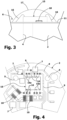
figure 3 is an enlarged detail of the sensor offigure 2 ; -
figure 4 is a plan view, partial and schematic, of a pressure sensor according to the invention, with some elements removed for more clarity of representation; -
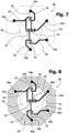
figures 5-8 are plan schematic views of a component of a pressure sensor according to the invention, in various steps of the respective production process; -
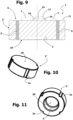
figure 9 is a schematic section, similar to that offigure 2 , illustrating a pressure sensor according to a possible variant of the invention. -
figures 10 and 11 are schematic perspective views, in different angles, of a body made of electrically insulating material useable for making a pressure sensor according to a further possible variant of the invention. - Hereinafter in the present description, terms such as "upper" and "lower" shall be intended as simple spatial reference to facilitate the description of the details illustrated in the figures.
- Indicated in its entirety with 1 in
figures 1 and 2 , is a pressure sensor according to the present invention. In the exemplified embodiment, thesensor 1 has amain body 2, preferably made of electrically insulating material, such as a ceramic material or the like, for example alumina,such body 2 being preferably - but not necessarily - monolithic and having a generally cylindrical shape, with some perimeter reference or positioning seats, one of which indicated with 2a. Defined in thebody 2 is a blind cavity or pressure chamber, indicated with 3 infigure 2 , departing from whose bottom is a throughhole 4, or pressure passage, such chamber and passage being preferably, but not necessarily, substantially coaxial to the axis of thebody 2. Thepassage 4 passes through thebody 2 completely, opening at the end or face of the body itself opposite to that on which thechamber 3 opens. - Defined in the
body 2 are further through holes, some of which are indicated with 5, passing through the body at a peripheral position with respect to thechamber 3 and thepassage 4. Preferably, at least the internal cylindrical surface of theseholes 5 is covered by a thin layer made of electrically conductive material, particularly a metal; hereinafter, theholes 5 shall be defined metallised holes for the sake of simplicity. - The
body 2 supports, on the upper surface thereof, a circuit arrangement or circuit, indicated in its entirety with 6, comprising a plurality of circuit components, conceived in a manner generally known in the art, and at least one integrated circuit. Thecircuit 6 is configured for obtaining the functionalities typically associated to the pressure sensors of the known type, for example prearranged for treating (detection, amplification, conditioning, processing) a signal representing the pressure, measured as described hereinafter. Some of the abovementioned circuit components, which are assumed to be resistors, capacitors and diodes, are indicated with 7, while indicated with 8 - solely infigure 1 - are terminals or pad contacts for the external electrical connection of thesensor 1. - According to a characteristic of the invention, made directly on the upper surface of the
body 2 is an electric circuit pattern, comprising a plurality of tracks made of electrically conductive material, not shown infigure 1 , screen printed or however deposited directly on said upper surface of thebody 2; also directly formed on the surface of thebody 2 may be circuit components, such as for example screen printed resistors. Thus, according to such characteristic, the ceramic material forming thebody 2 is exploited directly as a substrate for thecircuit 6 of thesensor 1, without requiring a special fibreglass printed circuit board, as it typically occurs in sensors according to the traditional art, and thus without even requiring to anchor such board to thebody 2. - The abovementioned tracks are arranged in such a manner to leave, on the upper surface of the
body 2, an area intended for mounting an integrated circuit or chip, described hereinafter free. Some of the abovementioned conductive tracks and resistors formed on the upper surface of thebody 2 are observable infigure 4 (wherein a protection layer, described hereinafter was not represented), respectively indicated with 9 and 10. Thecomponents 7 are connected, for example by means of welding, to thetracks 9, while the abovementioned chip is connected torespective tracks 9 orcomponents 7 through another technique, described hereinafter. Theterminal 8 may be obtained directly from therespective track portions 9 or, if configured as additional parts, they are connected to such tracks, for example by means of welding. - According to a preferred characteristic, the
tracks 9 and the possible screen printedresistors 10 are covered by a protection layer made of polymeric material, resistant to humidity, indicated with 11. Thelayer 11 is open locally, or it has windows, at least at the connection points of somecircuit components 7 at theconductive tracks 9. Thelayer 11 also has a local opening or window, indicated with 11a solely infigure 1 , at the mounting zone of the abovementioned chip. - According to another characteristic of the invention, the abovementioned chip belonging to the
circuit 6 is made up of a so-called "die", i.e. a small block or plate made of semiconductor material, typically silicon, which is bonded (diebonded) directly onto the upper surface of theceramic body 2, particularly gluebonded. Directly obtained in the abovementioned die, generally indicated with 15 infigures 2-4 , is the miniaturized electronic circuit of the integrated circuit which supervises the general operation of the pressure sensor. - In the example illustrated in
figures 2-4 , the die 15 is configured as a single plate or block made of silicon having a quadrangular section, but such solution shall not be intended as restrictive, given that thedie 15 may have shapes different from those illustrated and be made of a plurality of mutually joined parts or layers made of silicon. The die 15 is obtainable through techniques per se known in the industry for producing semiconductor chips. - The die 15 is without a package, and thus without respective projecting connection leads, typically obtained from relatively stiff metal elements, and directly positioned on the upper face thereof are contacts, some indicated with 15a in
figure 4 , in form of thin films made of electrically conductive material deposited on the die, preferably but not necessarily a noble material, such as for example gold or a 1% silicon aluminium alloy; preferred materials or alloys useable for the purpose may comprise gold, platinum, silicon, palladium, beryllium, silver, aluminium and copper. - According to a further characteristic of the invention, the connection of the
die 15 to theconductive tracks 9 and/or to thecomponents 7 of interest is obtained by means of added flexible contact elements, made up of thin wires made of electrically conductive material. The wires, some of which are indicated with 16 infigure 4 , are preferably but not necessarily made using noble metal, such as for example gold or a 1%, silicon aluminium alloy and have a diameter indicatively comprised between about 5 and 100 microns, preferably between about 25 and about 35 microns. Preferable materials or alloys useable for making the micro-wires 16 comprise gold, platinum, silicon, palladium, beryllium, silver, aluminium and copper. The micro-wires 16 are bonded or however connected between thecontacts 15a of thedie 15 and thetracks 9 and/or thecomponents 7 of interest of thecircuit 6, using processes of the known type such as "wire bonding", and particularly of the "wedge-bonding" or "ball-bonding" type, for example by means of thermocompression, or ultrasonic bonding, or thermosonic bonding; themicro-wires 16 may have different shapes or sections, such as a circular or quadrangular or substantially flat shape or section, for example flexible micro-ribbons made of conductive material. - Such characteristic, alongside allowing directly exploiting the ceramic material of the
body 2 as substrate even for thedie 15, allows avoiding bonding on thetracks 9 of the leads projecting from an integrated circuit, as it typically occurs according to the known surface mount technique, such projecting leads having a section and stiffness comparatively greater with respect to the micro-wires 16. In other words, the process of wire bonding used according to the invention determines welding points of minimum dimensions on thecircuit 6, performed on highly flexible connection elements (the wires 16): this allows an easier and more accurate positioning of the die, which may for example be definitely positioned at contact with said substrate, also allowing reducing the overall dimensions of thecircuit 6. - As mentioned, the
die 15 is not provided with its own package: for such reason, in the preferred embodiment of the invention, applied on thedie 15 and therespective connection micro-wires 16, as well as on the bonding region of such micro-wires 16 with thetracks 9 and/orcomponents 7 of interest, is a mass of a protective insulating material, such as a resin, particularly an epoxy resin, indicated with 17 infigures 1-3 (also theprotection 17 was not represented infigure 4 ), for example poured or dosed in liquid form and then left to harden. Themass 17, alongside protecting thedie 15, allows bonding it further to thebody 2, securing the position thereof. In a possible embodiment, the die 15 is directly bonded to thebody 2 by means of resin-bonding alone, or by means of theprotective mass 17 alone. - In an advantageous embodiment of the invention, the
pressure sensor 1 according to the invention is provided with temperature detector means, configured to detect the temperature of the sensor itself and/or of the substrate on which it is mounted, such parameter being particularly used by the control logic implemented in thedie 15 to compensate the pressure detections carried out; temperature detection is also useable by the control logic for protecting thesensor 1. - In a particularly advantageous embodiment of the invention, the abovementioned detector means include at least one temperature sensor incorporated or obtained directly in the die 15. Such embodiment is exemplified in
figure 3 , wherein the abovementioned temperature sensor is schematically represented by the block indicated with 18. In such manner, given that thedie 15 is practically mounted at direct contact with the surface of thebody 2, which provides the ceramic support of thecircuit 7, thetemperature sensor 18 is capable of accurately detecting the temperature of the body of thesensor 1. It should be observed that the typical integrated circuits with package and/or projecting connection leads, typically used in known pressure sensors, even when mounted through Surface Mount Device or SMD technique, still remain slightly raised or spaced by the respective circuit support and/or a portion of the material of the package remains interposed between the element made of semiconductor material and the body on which the SMD component is mounted, with ensuing slight detection errors: thus, the abovementioned preferred characteristic of the invention guarantees temperature detection with improved accuracy. - In possible variants, the
sensor 1 may be provided with several temperature detector means, intended to detect the environment temperature and/or indirectly the temperature of the fluid to be measured, for example with respective temperature sensors also mounted at different positions in the die and/or in the circuit, such as a sensor towards the environment (upwards) and a sensor towards the substrate (downwards). - With particular reference to
figure 2 , in the exemplified preferred embodiment of the invention, associated to the lower end of thebody 2 is a diaphragm body, indicated with 20, hereinafter defined as "diaphragm" for the sake of simplicity, preferably made of electrically insulating material, for example the same ceramic material used to make thebody 2. Thediaphragm 20 is provided with an electric detector element, capable of generating a signal representing a bending of the diaphragm itself; detection elements useable for the purpose may for example be selected from among resistor elements, capacitive elements and piezoresistitive elements. - Obtained on the body of the
diaphragm 20, and specifically on the surface thereof facing thebody 2, are electrically conductive tracks, for forming and/or connecting the abovementioned detection element which, strictly for exemplifying purposes, is assumed to be made up of a bridge of resistors. For example, referring tofigure 8 , the resistors, indicated with 21, are positioned or extend at least partly in a substantially central region of thediaphragm 20, or in a region subjected to elastic deformation, which in the mounted condition of the latter at least partly faces the interior of thechamber 3. Theresistors 21 are connected between the first ends of the abovementioned conductive tracks, indicated with 22, whose second ends are instead in a peripheral region of thediaphragm 20, preferably in a region not subjected to elastic deformation; the abovementioned second ends of thetracks 22 serve for electric connection of the detection means represented by the bridge ofresistors 21 to thecircuit 6, by means of themetallised holes 5, as observable hereinafter. In the example, theends 22a of thetracks 22 are substantially configured to form a pad, measuring a few hundreds of microns in size, indicatively comprised between about 200 x 200 and about 400 x 400 microns. - According to a preferred characteristic of the invention, the
diaphragm 20 is glue-bonded to themain body 2, in such a manner to obtain airtight closure of thechamber 3 on the lower side of thebody 2. Glue-bonding is carried out in such a manner that theconductive tracks 22, and more precisely theconnection end 22a thereof, are positioned at the lower ends of themetallised holes 5, and in such a manner to allow, due to the subsequent deposition of a conductive material, such as glue, electric connection with the conductive material that covers the surfaces of the holes themselves. Obviously, in the design step, the geometry of thetracks 22 and the position of therespective ends 22a is selected for the purpose. - As observable, the upper ends of the
metallised holes 5 are in turn electrically connected to some of theconductive tracks 9 belonging to thecircuit 6, which are located on the upper surface of thebody 2, in such a manner that the detector part incorporated on thediaphragm 20 is electrically connected or in signal communication with thecircuit 6. - In the embodiment of the invention illustrated in the figures, the
sensor 1 is provided for the detection of a relative pressure, i.e. it is configured for measuring the pressure applied to thediaphragm 20 with respect to the environment pressure; for such purpose, thepassage 4 is open at the upper face of thebody 2. The same sensor structure illustrated in the figures is however useable for obtaining absolute pressure sensors, by simply closing thepassage 4 at the upper end, for example by means of a tin drop. In this second case, present in theinternal chamber 3 and in thepassage 4 may be two conditions: vacuum, created in a per se known manner in the production step, or a predefined pressure, such as the environment pressure existing during production, i.e. when occluding thepassage 4, which defines the sensor as a "seal gauge sensor". - The general operation of the
pressure sensor 1 occurs according to known methods, and thus it shall not be described herein in detail. Generally, in practical use, thesensor 1 may be mounted in a device for detecting the pressure of fluids (liquid and aeriform substances), such as in the automotive industry, household and household appliances industry, air conditioning and in the hydro-sanitary heating industry in general. Such device has a housing defining an inlet which receives a fluid to be subjected to pressure detection, thesensor 1 being mounted in the housing such that thediaphragm 20 shall be exposed to the fluid. The mechanical deformation of thediaphragm 20, due to the pressure of the fluid subjected to measurement, modifies the resistance value in output from the bridge ofresistors 21. Thecircuit 6 detects the output signal from the bridge of resistors, by means ofmetallised holes 5, and process it according to per se known methods (possible amplification and/or conditioning and/or processing), then making it available to the outside by means of theterminals 8 offigure 1 , possibly connected to a suitable electric connector associated to the abovementioned housing. - As mentioned, the
circuit 6 is configured to obtain the functionalities typically associated to pressure sensors of the known type. As outlined previously, according to a preferred characteristic of the invention, thesensor 1 is further provided with temperature detector means, preferably incorporated in thedie 15, which allow compensating the performed temperature detections. - According to possible variants, the sensor may be provided with further temperature sensor means, for example mounted in proximity to the diaphragm and/or the resistive sensor bridge, connected to the
circuit 6 and/or to thedie 15. - The
die 15 provides a digital processor, such as a microprocessor or microcontroller circuit, which can be provided with - or have associated thereto - electronic memory means, preferably of the non-volatile and/or electronically rewritable type, such as for example of the EEPROM or Flash type, such memory means MEM being suitable to store information permanently even in the absence of power supply. - The
control part sensor 1 is configured to detect and condition the signal of the resistive bridge, generating a ratiometric signal amplified at the output, preferably variable between 0.5 V and 4.5 V, by means of the threeterminals 8. Thecontrol part sensor 18. The circuit parts that implement the conditioning of the signals of the resistive bridge and/or of the temperature detector means may for example comprise an amplifier stage or a voltage divider. The amplifier stage may preferably be calibrated or adjusted by varying at least one external parameter, such as a resistive value. Such variation of the external parameter may be obtained by means of a calibration circuit part, which may comprise, for the purpose, a digital potentiometer. Thedie 15 is also preferably configured for periodically detecting the degree of accuracy of the sensor, such as the accuracy of the bridge and temperature sensor means, by performing - when required - an automatic calibration of the respective conditioning circuit part. Also for such purpose, thecircuit 6 may be additionally provided with functionalities for compensating possible drifts or "offsets", for example for each sensor provided for, controlled by thedie 15. - Furthermore, preferably, the
control part - an incorporated ESD protection (protection/shielding against electromagnetic interferences);
- protection against overvoltage and/or protection against polarity inversion;
- calibration and self-calibration functions, for example such as calibration or programming during the production step or self-calibration during periodic testing and automatic calibration, or aging detection, i.e. correction of pressure detections due to elapsed time;
- functions regarding programming or memorising or reading parameters or data or program instructions, such as a transmission or writing and/or data reception or reading or parameters or instructions, preferably after the assembly of the
control part terminals 8, which also serve as an output for the measurement signals generated by thepressure sensor 1. - Furthermore, still preferably, the
control part - Following is a preferred method for making the
sensor 1. -
Conductive tracks 22 are formed on the ceramic body of thediaphragm 20 by means of deposition - preferably through silk-screen printing technique - of a conductive material, such as for example a silver-palladium alloy; the result of such step is schematically represented infigure 5 . After depositing the material there follows drying and baking of the semi-finished product offigure 5 , with suitable temperatures and times depending on the material used. - Then, the material intended to form the
resistors 21, for example a resistive paste 10k preferably silk-screen printed, is deposited on thediaphragm 20, as schematized infigure 6 , in such a manner to obtain the detection element, or the resistive bridge. Also in this case, after depositing the material, there follows the drying and baking of the semi-finished product offigure 6 , with suitable temperatures and times. - Then, a layer of protective material, particularly glass, is deposited on the
diaphragm 20, preferably by means of silk-screen printing, in such a manner to cover the detection element, or the resistive bridge; such protective layer made of glass is indicated with 23 infigure 7 . Also in this case, after depositing the material, there follows the drying and baking of the semi-finished product offigure 7 , with suitable temperatures and time. - Then, a layer of adhesive material or glue, indicated with 24 in
figure 8 , is deposited on thediaphragm 20, also in this case preferably by means of silk-screen printing. The useable adhesive may also for example be a low or medium melting temperature glass paste or a thermosetting resin. As observable, theadhesive layer 24 is configured in such a manner not to cover neither the central zone of thediaphragm 20, present in which is the detection part covered by theglass layer 23, nor somelocal zones 24a surrounding the connection ends 22a of thetracks 22. Also in this case, after depositing the adhesive layer, there follows the drying and baking of the semi-finished product offigure 8 . - Regarding the obtainment of the
circuit part 6 provided for on themain body 2, the first step of the process is preferably the metallisation of theholes 5; as mentioned, for such purpose a layer made of metal or another electrically conductive material is deposited, through per se known methods, on the surface of theholes 5. This deposition is preferably carried out in such a manner that part of the metal or conductive material projects outside theholes 5 at the corresponding ends, for example partly on the lower and upper surfaces of thebody 2. After depositing the material there follows the drying and baking of the semi-finished product, with suitable temperatures and time. - Then, the
conductive tracks 9 are formed on the upper face of thebody 2, by means of deposition - preferably through silk-screen printing technique - of a conductive material, such as for example a silver-palladium alloy; then, there follows the respective steps of drying and baking. Thetracks 9 may possibly be deposited in such a manner to be electrically at contact with the conductive material of theholes 5, or with the part of such material projecting outside the holes themselves; alternatively, the ends of thetracks 9 may be put to contact with themetallised holes 5 by depositing an additional conductive material, as explained hereinafter. - A thin layer of the same material forming the micro-wires 16, or compatible with the material forming the micro-wires, is deposited on the ends of the
tracks 9 which shall be connected to the die 15 by means of micro-wires 16 (figures 3 and 4 ), preferably by means of silk-screen printing. Also in this case, the deposition of the material is followed by respective drying and baking steps. - Then, there follows the deposition, still on the upper surface of the
body 2, of a material intended to obtain thepossible resistors 10 offigure 4 . The material in question may be for example a resistive paste, deposited by means of silk-screen printing; obviously, such material is deposited in such a manner that the obtainedresistors 10 are electrically at contact with respectiveconductive tracks 9. Also in this case, after depositing the material there follows the drying and baking of the semi-finished product, with suitable temperatures and time. - Then, a layer of an adhesive or glue is deposited on the face of the
body 2 opposite to thecircuit 6, by means of silk-screen printing, with subsequent drying and baking steps. The adhesive is preferably of the same type as that used for making thelayer 24 provided for on the diaphragm 20 (figure 8 ). As evincible, the deposition of the adhesive material is limited to the peripheral zone of the abovementioned lower face of thebody 2, i.e. the region of such face delimiting the opening of thecavity 3 offigure 2 . - Then, the two
body parts sensor 1 are bonded to each other. For such purpose, theadhesive layer 24 of thediaphragm 20 is placed on the adhesive layer present on the lower face of thebody 2. As mentioned previously, the relative positioning is such that the connection ends 22a of thetracks 22 of the diaphragm (seefigure 8 ) are overlapped and at contact with the conductive material of theholes 5, on the lower surface of thebody 2. Certainty of electric contact is preferably ensured by dosing a conductive paste or epoxy glue into theholes 5, which fills the interspace between the hole itself and the respective connection end orpad 22a, hence guaranteeing contact. - Then, there follows a baking step, required to obtain adhesion between the two abovementioned adhesive layers, and thus the perfect sealed adhesion between the parts, and possibly an at least partial melting of the electrically conductive material to obtain or improve electric connections; this baking step is preferably followed by a hermeticity test, performed in per se known manners.
- If required, the upper ends of the
metallised holes 5 may be put to electric contact with therespective tracks 9, by means of local deposition of a conductive paste or glue, in the respective interface zones; also this step, when provided for, is followed by a drying and baking operation. Alternatively, provided for may be the sole reflow of at least part of the previously deposited electrically conductive materials, in particular in the zone between the body and diaphragm. - The detection element provided for on the
diaphragm 20, i.e. the resistive bridge, is thus balanced or calibrated, through per se known methods. - Then, there follows the deposition, preferably by means of silk-screen printing, of the polymeric material intended to provide the
protective layer 11 offigures 1-3 , followed by the relative drying and baking. As outlined previously, thelayer 11 is deposited in such a manner to leave the zones in which thecomponents 7 of thecircuit 6 shall be connected to theconductive tracks 9 exposed. Furthermore, thelayer 11 is deposited in such a manner to leave, by means of thewindow 11a, also the region of the upper surface of thebody 2 in which thedie 15 is to be glued, directly exposed; obviously also exposed in such region are the ends of thetracks 9 to which the micro-wires 16 are to be connected. - At this point, the
components 7 of thecircuit 6 are mounted on the upper part of thebody 2, preferably by means of the SMD technique. As evincible, in such step, the leads for connecting thecomponents 7 in question are connected electrically with the respective tracks 9. Then, there follows a reflow welding. - After such step, the
die 15 is bonded, particularly by means of gluing, onto the upper surface of thebody 2, at the dedicated zone not occupied by thetracks 9 or other components of thecircuit 6, and left exposed by theprotective layer 11. The step comprises the deposition of a suitable conductive adhesive or glue, on at least one of the lower face of thedie 15 and the corresponding positioning zone on the surface of thebody 2. Preferably, this conductive adhesive has good thermal conduction characteristics, in particular with the aim of facilitating the measurement of temperature by thetemperature sensor 18 inside thedie 15 and/or guarantee good thermal dissipation. - After gluing the die 15 there follows the step of electric connection or wire bonding, i.e. the connection of the micro-wires 16, between the
respective contacts 15a of thedie 15 and the ends of theconductive tracks 9 in question, according to a per se known technique. - At this point, the insulating
protection 17 offigures 1-3 - as mentioned for example made up of a mass of resin, preferably an epoxy resin - is deposited on thedie 15 and the respective connection micro-wires 16, as well as on the bonding region ofsuch micro-wires 16 with thetracks 9 and/orcomponents 7 of interest. Then, there follows a step of polymerising such material. - Should the
sensor 2 be of the absolute type, the upper end of thepassage 4 must be closed hermetically: thus, in such case, a drop of suitable material, for example tin, is deposited - under a vacuum environment - preferably by means of silk-screen printing or welding, to close the abovementioned end. - Then, there follows the welding of the connection terminals or
wires 8 offigure 1 to thetracks 9 of interest of thecircuit 6, required for the connection of thesensor 1 for use thereof. Then, the sensor, and in particular the die 15, is calibrated electronically. For such purpose, it should be observed that the detection element or the resistive bridge or the respective control circuit, is preferably of the digital calibration type. - It is clear that the sensor described for exemplification purposes may be subjected - by a man skilled in the art - to numerous variants, without departing from the scope of the invention as defined in the attached claims.
- The invention was described with reference to a pressure sensor in which the
diaphragm 20 is configured as an additional part, in particular glue-bonded, to a further base, i.e. themain body 2. The base concepts of the invention are however applicable even in the case of pressure sensors having abase 2 without ahole 4, exclusively with the "seal gauge" configuration or having a monolithic body, integrally defining the respective diaphragm. - An example of the abovementioned first type sensor is illustrated in
figure 9 , where the abovementioned body or base without through hole is indicated in its entirety with 2'.Such sensor 1 may be used in case of medium and high pressures, offering greater safety due to a more solid structure. - An example of a sensor with a monolithic body is instead illustrated schematically in
figures 10 and 11 , where such body is indicated in its entirety with 2". In the illustrated example, themonolithic body 2", generally cylindricalshaped, with some peripheral reference or positioning seats, is made at least partly of an electrically insulating material, such as a ceramic material, and has a blind cavity 3', substantially circular-shaped, closed at one end by a diaphragm portion 20' of the body itself. In such embodiment, provided for at the diaphragm portion 20', particularly in a central region of an upper surface thereof, is the detector component, suitable to generate the signal representing a bending of the diaphragm portion itself, as well as a circuit having the characteristics of the one indicated previously with 6. Such circuit may be possibly formed entirely or partly in the peripheral zone of the upper surface of the body 2', i.e. in the annular region of the upper face of the body 2' surrounding the diaphragm portion 20'. - In a further possible variant, the temperature detector means of the sensor according to the invention may comprise a temperature sensor mounted on the
diaphragm 20, facing into thechamber 3 and in signal communication with thecircuit 6 including the die 15 by means of relative conductive tracks and metallised holes, conceptually similar to those previously indicated with 22 and 5. - The
tracks 9 and/orpossible resistors 10 may be obtained on the sensor body by means of a technique different from silk-screen printing, though it is the preferred technique; for example, alternative techniques for the tracks and/or resistors of the sensor may be selected from among lithography, photolithography, spraying conductive material, surface metallisation, plating, etcetera.
Claims (15)
- A pressure sensor having a sensor body (2, 20; 2', 20; 2", 20') with a diaphragm (20; 20'), the sensor body (2, 20; 2', 20; 2", 20') and the diaphragm (20; 20') being at least partly formed with an electrically insulating material, particularly a ceramic material, and defining a cavity (3; 3'), the diaphragm (20; 20') at least partly facing said cavity (3; 3') and having thereon at least part of a detection element (21, 22) configured for detecting a bending or deformation of the diaphragm (20; 20'), wherein the sensor body (2, 20; 2', 20; 2", 20') supports a circuit arrangement (6), in signal communication with the detection element (21, 22) and comprising a plurality of circuit components (7, 10, 15), among which an integrated circuit (15), the circuit arrangement (6) being prearranged for treating a signal generated by the detection element (21, 22), characterized in that- the said integrated circuit consists of a die made of a semiconductor material (15);- the circuit arrangement (6) includes an electric circuit pattern comprising a plurality of tracks made of electrically conductive material (9) directly deposited onto a first surface of the sensor body (2, 20; 2', 20; 2", 20') that is made of electrically insulating material, said tracks (9) being organized such that a region of said first surface is directly exposed for the mechanical bonding, particularly through glue-bonding or resin-bonding, of the said die (15);- the die (15) is directly bonded to said first surface, at said region, i.e., a zone not occupied by said tracks (9);- said die (15) is connected to respective said tracks (9) by wire bonding, i.e., by means of thin flexible connecting wires (16), made of an electrically conductive material.
- The sensor according to claim 1, wherein the wires are flexible micro-wires (16) having a thickness or diameter comprised between about 5 and 100 micron, particularly between about 25 to about 35 micron, and being preferably formed by a material or an alloy comprising, or based on a material selected from among gold, platinum, silicon, palladium, beryllium, silver, aluminium and copper.
- The sensor according to claim 1 or 2, further comprising temperature detector means (18), particularly connected to, or comprised within, or integrated into said element or die made of semiconductor material (15).
- The sensor according to claim 1 or 2, wherein said element or die made of semiconductor material (15) and the corresponding said wires (16), as well as at least part of the region of connection of said wires (16) with respective said tracks (9), is coated with a mass of a protective insulating material (17), such as a resin, particularly an epoxy resin.
- The sensor according to claim 1, wherein said tracks (9) are coated with a protection layer (11), particularly a polymeric material, the protection layer (11) being locally open, i.e., having windows, at least at connection zones of at least some of said circuit components (7) to respective said conductive tracks (9), the protection layer (11) further having o local opening or window (11a) at said positioning region.
- The sensor according to claim 1, wherein on at least one face or side of said element or die of semiconductor material (15) contacts (15a) are provided, consisting of thin films made of electrically conductive material, for the connection of said wires (16).
- The sensor according to claim 1, wherein said circuit components (7-10, 15) comprise one or more resistors (10), preferably formed by a resistive material directly deposited onto said first surface.
- The sensor according to claim 5 and 7, wherein said resistors (10) are at least partly coated with said protection layer (11).
- The sensor according to one or more of the preceding claims, wherein the sensor body (2, 20; 2', 20) comprises a first body part (2; 2'), that supports said circuit arrangement (6), and a second body part (20), defining said diaphragm, the first and the second body part (2, 20; 2', 20) being mutually fixed or bonded, particularly by means of an adhesive material, and wherein:- the first body part (2, 2') defines a blind cavity (3) which opens on a first face of the first body part (2, 2');- the circuit arrangement (6) is on a second face of the first body part (2, 2') which is opposite to said first face; and- the second body part (20) is fixed of glue-bonded to said first face so as to form a bottom of said cavity (3).
- The sensor according to claim 9, wherein in the first body part (2; 2') through-holes are provided (5), extending between said first and second face, and wherein- at least one inner surface of said through-holes (5) is coated with a layer made of an electrically conductive material for connecting said detection element (22, 21) to said circuit arrangement (6), and/or- said through-holes (15) are at least partly filled with an electrically conductive material, such as a conductive paste or glue, in particular for connecting said through-holes to electric components or elements (21, 22) present on the diaphragm (20).
- The sensor according to claim 9, wherein the first body part (2) has a through-opening (4) extending from a bottom of said cavity (3) and said second face, and wherein:- if the pressure sensor (1) is a relative pressure sensor, said through-opening (4) is open at the corresponding end that opens on said second face; and- if the pressure sensor (1) is an absolute pressure sensor, said through-opening (4) is closed at the corresponding end that opens on said second face.
- The sensor according to claim 1, wherein the circuit arrangement (6) is prearranged for performing one or more functions selected from ESD protection, over-voltage protection, polarity-inversion protection, aging detection, automatic calibration, digital calibration, data or parameters programming,
where in particular the circuit arrangement (6) and/or the said integrated circuit or die (15) is configured for being programmed or calibrated after the relevant assembly on the sensor body (2), preferably by means of the same terminal (8) which are then used as output for the measure signals generated by the sensor (1). - The sensor according to claim 1, wherein the circuit arrangement (6) is configured to have a ratiometric signal output, i.e., with an output voltage depending upon the supply voltage, being preferably variable between 0.5 and 4.5 V.
- A process for manufacturing a pressure sensor according to one or more of claims 1 to 13, comprising the steps of:- obtaining said tracks (9) on said first surface (9), so as to leave said positioning region of the sensor body (2, 20; 2', 20; 2", 20') directly exposed;- depositing, at least onto end zones of the said tracks (9) that have to be connected to said die (15), a layer of the same material constituting said wires (16) or a material compatible with the material forming said wires;- bonding said die (15) in said positioning region of said first surface, particularly by glue-bonding;- connecting by wire bonding said die (15) to respective said tracks (9);- coating said die (15) and the corresponding said wires (16), as well as the region of connection of said wires (16) with respective said tracks (9), with said mass (17) made of a protective insulating material.
- A pressure detecting device, comprising a pressure sensor according to one or more of claims 1 to 13.
Applications Claiming Priority (2)
| Application Number | Priority Date | Filing Date | Title |
|---|---|---|---|
| ITTO2009A000384A IT1394791B1 (en) | 2009-05-20 | 2009-05-20 | PRESSURE SENSOR |
| PCT/IB2010/052247 WO2010134043A1 (en) | 2009-05-20 | 2010-05-20 | Pressure sensor |
Publications (2)
| Publication Number | Publication Date |
|---|---|
| EP2433107A1 EP2433107A1 (en) | 2012-03-28 |
| EP2433107B1 true EP2433107B1 (en) | 2024-02-21 |
Family
ID=41506455
Family Applications (1)
| Application Number | Title | Priority Date | Filing Date |
|---|---|---|---|
| EP10728294.9A Active EP2433107B1 (en) | 2009-05-20 | 2010-05-20 | Pressure sensor |
Country Status (8)
| Country | Link |
|---|---|
| US (1) | US8878313B2 (en) |
| EP (1) | EP2433107B1 (en) |
| CN (1) | CN102460101B (en) |
| BR (1) | BRPI1011105B1 (en) |
| IT (1) | IT1394791B1 (en) |
| PL (1) | PL2433107T3 (en) |
| RU (1) | RU2521869C2 (en) |
| WO (1) | WO2010134043A1 (en) |
Families Citing this family (29)
| Publication number | Priority date | Publication date | Assignee | Title |
|---|---|---|---|---|
| DE102011005274B4 (en) * | 2011-03-09 | 2020-09-10 | Endress+Hauser SE+Co. KG | Ceramic pressure measuring cell |
| ITTO20120293A1 (en) * | 2012-04-03 | 2013-10-04 | Metallux Sa | PROCEDURE FOR CALIBRATING A CALIBRATION ELEMENT AND ITS DEVICE |
| ITTO20121130A1 (en) * | 2012-12-21 | 2014-06-22 | Metallux Sa | PRESSURE SENSOR |
| DE102013101315A1 (en) | 2013-02-11 | 2014-08-14 | Endress + Hauser Gmbh + Co. Kg | Method for soldering a connection element |
| AT515070B1 (en) * | 2013-10-30 | 2020-01-15 | Melecs Ews Gmbh & Co Kg | Method for contacting and fastening ceramic pressure sensors on a printed circuit board |
| US10620070B2 (en) | 2014-12-23 | 2020-04-14 | Eltek S.P.A. | Pressure sensor including overmolded element(s) for securing positioning |
| DE102015104410B4 (en) * | 2015-03-24 | 2018-09-13 | Tdk-Micronas Gmbh | pressure sensor |
| ITUB20150460A1 (en) | 2015-04-16 | 2016-10-16 | Metallux Sa | SENSOR FOR DETECTION OF ONE OR MORE QUANTITIES OF A FLUID, PARTICULARLY A PRESSURE SENSOR |
| US10024747B2 (en) * | 2015-06-19 | 2018-07-17 | Merit Medical Systems, Inc. | Pressure ports and related methods |
| ITUA20163990A1 (en) | 2016-05-31 | 2017-12-01 | St Microelectronics Srl | MINIATURIZED LOAD SENSOR DEVICE WITH REDUCED SENSITIVITY TO THERMO-MECHANICAL STRENGTHENING OF STRENGTHENING, IN PARTICULAR STRENGTH AND PRESSURE SENSOR |
| EP3903674B1 (en) * | 2016-08-31 | 2025-08-13 | Nipro Corporation | Guide wire and method for manufacturing guide wire |
| ES3048232T3 (en) | 2016-08-31 | 2025-12-09 | Nipro Corp | Guide wire and method for manufacturing guide wire |
| US9878904B1 (en) | 2016-10-25 | 2018-01-30 | Rosemount Aerospace Inc. | MEMS sensor with electronics integration |
| US10466125B2 (en) * | 2016-11-11 | 2019-11-05 | Measurement Specialties Inc. | Pressure sensor sub assembly and fabrication |
| US10481025B2 (en) | 2017-01-26 | 2019-11-19 | Rosemount Aerospace Inc. | Piezoresistive sensor with spring flexures for stress isolation |
| EP3355032B1 (en) * | 2017-01-30 | 2019-03-27 | Dr. Johannes Heidenhain GmbH | Sensor for position measurement |
| DE102017219986A1 (en) * | 2017-11-09 | 2019-05-09 | Robert Bosch Gmbh | Pressure sensor module and pressure sensor device with a pressure sensor module |
| DE102018221984A1 (en) * | 2018-12-17 | 2020-06-18 | Robert Bosch Gmbh | Method for producing a sensor request for determining at least one pressure of a fluid medium |
| EP3671160B1 (en) | 2018-12-21 | 2024-07-31 | Exentis Knowledge GmbH | Mould and method for manufacturing the same |
| EP3671159B1 (en) | 2018-12-21 | 2022-12-21 | Exentis Knowledge GmbH | Body formed by an additive manufacturing method and method for manufacturing the same |
| EP3671161B1 (en) | 2018-12-21 | 2025-01-29 | Exentis Knowledge GmbH | Mould and method for manufacturing the same |
| CN209326840U (en) | 2018-12-27 | 2019-08-30 | 热敏碟公司 | Pressure sensor and pressure transmitter |
| CN109799026B (en) * | 2019-03-19 | 2021-12-17 | 中国电子科技集团公司第十三研究所 | MEMS pressure sensor and preparation method |
| CN110672943B (en) * | 2019-09-26 | 2022-11-08 | 宁波大学 | Aging Detection Sensor Based on Voltage Comparator |
| IT201900019274A1 (en) * | 2019-10-18 | 2021-04-18 | Metallux Sa | PRESSURE SENSOR |
| ES2986136T3 (en) * | 2020-09-21 | 2024-11-08 | Brimind S R L | Electronic pressure sensor with improved sealing system |
| CN113155348B (en) * | 2021-02-26 | 2023-09-12 | 西安微电子技术研究所 | Piezoresistive pressure sensor signal processing module and integration method thereof |
| JP2024006068A (en) * | 2022-06-30 | 2024-01-17 | 株式会社鷺宮製作所 | pressure sensor |
| IT202300016326A1 (en) * | 2023-08-01 | 2025-02-01 | Eltek Spa | PRESSURE SENSOR DEVICE |
Citations (7)
| Publication number | Priority date | Publication date | Assignee | Title |
|---|---|---|---|---|
| US5407501A (en) * | 1992-01-24 | 1995-04-18 | The Foxboro Company | Method of manufacture of pressure sensor having a laminated substrate |
| US5561247A (en) * | 1993-03-30 | 1996-10-01 | Honda Motor Co., Ltd. | Pressure sensor |
| US5571970A (en) * | 1993-03-30 | 1996-11-05 | Honda Motor Co., Ltd. | Pressure sensor |
| US5629486A (en) * | 1996-01-25 | 1997-05-13 | Delco Electronics Corporation | Pressure sensor apparatus with integrated circuit mounted thereon |
| WO2001053789A1 (en) * | 2000-01-19 | 2001-07-26 | Silicon Valley Sensors, Inc. | Isolation technique for pressure sensing structure |
| JP2003042873A (en) * | 2001-07-30 | 2003-02-13 | Kyocera Corp | Package for pressure detector |
| EP2136193A2 (en) * | 2008-06-19 | 2009-12-23 | Eltek S.p.A. | Pressure sensor device |
Family Cites Families (9)
| Publication number | Priority date | Publication date | Assignee | Title |
|---|---|---|---|---|
| US4815472A (en) * | 1987-06-01 | 1989-03-28 | The Regents Of The University Of Michigan | Multipoint pressure-sensing catheter system |
| US5207103A (en) * | 1987-06-01 | 1993-05-04 | Wise Kensall D | Ultraminiature single-crystal sensor with movable member |
| RU2034247C1 (en) * | 1991-02-20 | 1995-04-30 | Государственный университет "Львивська политехника" | Temperature sensitive element |
| US5457878A (en) * | 1993-10-12 | 1995-10-17 | Lsi Logic Corporation | Method for mounting integrated circuit chips on a mini-board |
| DE19614458C2 (en) * | 1996-04-12 | 1998-10-29 | Grundfos As | Pressure or differential pressure sensor and method for its production |
| DE10140617A1 (en) * | 2001-08-18 | 2003-03-06 | Bosch Gmbh Robert | Measuring system with ratiometric frequency output |
| CN100443873C (en) * | 2004-09-28 | 2008-12-17 | Vega格里沙贝两合公司 | For sensors fixed on vessels, especially pressure sensors |
| US7373843B2 (en) * | 2005-06-02 | 2008-05-20 | Fidelica Microsystems | Flexible imaging pressure sensor |
| US7713771B2 (en) * | 2006-09-01 | 2010-05-11 | Grundfos A/S | Pressure sensor |
-
2009
- 2009-05-20 IT ITTO2009A000384A patent/IT1394791B1/en active
-
2010
- 2010-05-20 RU RU2011152005/28A patent/RU2521869C2/en active
- 2010-05-20 WO PCT/IB2010/052247 patent/WO2010134043A1/en not_active Ceased
- 2010-05-20 US US13/321,373 patent/US8878313B2/en active Active
- 2010-05-20 BR BRPI1011105-0A patent/BRPI1011105B1/en active IP Right Grant
- 2010-05-20 CN CN201080022596.5A patent/CN102460101B/en active Active
- 2010-05-20 EP EP10728294.9A patent/EP2433107B1/en active Active
- 2010-05-20 PL PL10728294.9T patent/PL2433107T3/en unknown
Patent Citations (7)
| Publication number | Priority date | Publication date | Assignee | Title |
|---|---|---|---|---|
| US5407501A (en) * | 1992-01-24 | 1995-04-18 | The Foxboro Company | Method of manufacture of pressure sensor having a laminated substrate |
| US5561247A (en) * | 1993-03-30 | 1996-10-01 | Honda Motor Co., Ltd. | Pressure sensor |
| US5571970A (en) * | 1993-03-30 | 1996-11-05 | Honda Motor Co., Ltd. | Pressure sensor |
| US5629486A (en) * | 1996-01-25 | 1997-05-13 | Delco Electronics Corporation | Pressure sensor apparatus with integrated circuit mounted thereon |
| WO2001053789A1 (en) * | 2000-01-19 | 2001-07-26 | Silicon Valley Sensors, Inc. | Isolation technique for pressure sensing structure |
| JP2003042873A (en) * | 2001-07-30 | 2003-02-13 | Kyocera Corp | Package for pressure detector |
| EP2136193A2 (en) * | 2008-06-19 | 2009-12-23 | Eltek S.p.A. | Pressure sensor device |
Also Published As
| Publication number | Publication date |
|---|---|
| WO2010134043A1 (en) | 2010-11-25 |
| US8878313B2 (en) | 2014-11-04 |
| RU2011152005A (en) | 2013-06-27 |
| BRPI1011105B1 (en) | 2019-10-15 |
| IT1394791B1 (en) | 2012-07-13 |
| EP2433107A1 (en) | 2012-03-28 |
| BRPI1011105A2 (en) | 2016-03-15 |
| PL2433107T3 (en) | 2024-07-08 |
| US20120104518A1 (en) | 2012-05-03 |
| CN102460101B (en) | 2014-11-26 |
| RU2521869C2 (en) | 2014-07-10 |
| CN102460101A (en) | 2012-05-16 |
| ITTO20090384A1 (en) | 2010-11-21 |
Similar Documents
| Publication | Publication Date | Title |
|---|---|---|
| US8878313B2 (en) | Pressure sensor | |
| US7600422B2 (en) | Electronic components packaging structure | |
| EP2765410B1 (en) | Gas sensor package | |
| CN103376279B (en) | Humidity sensor apparatus | |
| JP5212133B2 (en) | Flow type sensor | |
| KR20150083029A (en) | Sensor for detecting a temperature and a pressure of a fluid medium | |
| JP2004513339A (en) | Pressure sensor module | |
| EP2230507A1 (en) | Humidity or gas sensor | |
| US20170113924A1 (en) | Sensor component having two sensor functions | |
| JP5125978B2 (en) | Sensor device | |
| JPS61176832A (en) | Transducer-insert, manufacture thereof and mechanical variation measuring sensor | |
| CN105209877B (en) | Pressure sensor | |
| CN113518906A (en) | Measuring device with sensor element and measuring and operating circuit | |
| US10651609B2 (en) | Method of manufacturing physical quantity sensor device and physical quantity sensor device | |
| JP2007127612A (en) | Humidity sensor device and its manufacturing method | |
| JPWO2003063258A1 (en) | Semiconductor device | |
| CN114787603B (en) | Pressure sensor | |
| CN107490337B (en) | Strain detector and method for manufacturing the same | |
| CN101305266A (en) | Sensors, sensor components and methods for manufacturing sensors | |
| CN107631819B (en) | Low cost overmolded leadframe force sensor with multiple mounting positions | |
| JP4807199B2 (en) | Humidity sensor device | |
| JP2006010547A (en) | Humidity sensor module and humidity sensor mounting structure | |
| CN109696215B (en) | Sensor assembly for determining a parameter of a fluid medium of a measuring channel and method for producing the same | |
| EP3548848B1 (en) | Integrated circuit sensor package and method of manufacturing the same | |
| JP5825181B2 (en) | Humidity sensor |
Legal Events
| Date | Code | Title | Description |
|---|---|---|---|
| PUAI | Public reference made under article 153(3) epc to a published international application that has entered the european phase |
Free format text: ORIGINAL CODE: 0009012 |
|
| 17P | Request for examination filed |
Effective date: 20111117 |
|
| AK | Designated contracting states |
Kind code of ref document: A1 Designated state(s): AL AT BE BG CH CY CZ DE DK EE ES FI FR GB GR HR HU IE IS IT LI LT LU LV MC MK MT NL NO PL PT RO SE SI SK SM TR |
|
| DAX | Request for extension of the european patent (deleted) | ||
| 17Q | First examination report despatched |
Effective date: 20160819 |
|
| STAA | Information on the status of an ep patent application or granted ep patent |
Free format text: STATUS: EXAMINATION IS IN PROGRESS |
|
| GRAP | Despatch of communication of intention to grant a patent |
Free format text: ORIGINAL CODE: EPIDOSNIGR1 |
|
| STAA | Information on the status of an ep patent application or granted ep patent |
Free format text: STATUS: GRANT OF PATENT IS INTENDED |
|
| INTG | Intention to grant announced |
Effective date: 20230627 |
|
| GRAS | Grant fee paid |
Free format text: ORIGINAL CODE: EPIDOSNIGR3 |
|
| GRAJ | Information related to disapproval of communication of intention to grant by the applicant or resumption of examination proceedings by the epo deleted |
Free format text: ORIGINAL CODE: EPIDOSDIGR1 |
|
| GRAL | Information related to payment of fee for publishing/printing deleted |
Free format text: ORIGINAL CODE: EPIDOSDIGR3 |
|
| STAA | Information on the status of an ep patent application or granted ep patent |
Free format text: STATUS: EXAMINATION IS IN PROGRESS |
|
| GRAP | Despatch of communication of intention to grant a patent |
Free format text: ORIGINAL CODE: EPIDOSNIGR1 |
|
| STAA | Information on the status of an ep patent application or granted ep patent |
Free format text: STATUS: GRANT OF PATENT IS INTENDED |
|
| INTC | Intention to grant announced (deleted) | ||
| INTG | Intention to grant announced |
Effective date: 20231114 |
|
| GRAA | (expected) grant |
Free format text: ORIGINAL CODE: 0009210 |
|
| STAA | Information on the status of an ep patent application or granted ep patent |
Free format text: STATUS: THE PATENT HAS BEEN GRANTED |
|
| AK | Designated contracting states |
Kind code of ref document: B1 Designated state(s): AL AT BE BG CH CY CZ DE DK EE ES FI FR GB GR HR HU IE IS IT LI LT LU LV MC MK MT NL NO PL PT RO SE SI SK SM TR |
|
| REG | Reference to a national code |
Ref country code: GB Ref legal event code: FG4D |
|
| REG | Reference to a national code |
Ref country code: CH Ref legal event code: EP |
|
| REG | Reference to a national code |
Ref country code: DE Ref legal event code: R096 Ref document number: 602010069250 Country of ref document: DE |
|
| REG | Reference to a national code |
Ref country code: IE Ref legal event code: FG4D |
|
| P01 | Opt-out of the competence of the unified patent court (upc) registered |
Effective date: 20240229 |
|
| REG | Reference to a national code |
Ref country code: SE Ref legal event code: TRGR |
|
| REG | Reference to a national code |
Ref country code: LT Ref legal event code: MG9D |
|
| REG | Reference to a national code |
Ref country code: NL Ref legal event code: MP Effective date: 20240221 |
|
| PG25 | Lapsed in a contracting state [announced via postgrant information from national office to epo] |
Ref country code: IS Free format text: LAPSE BECAUSE OF FAILURE TO SUBMIT A TRANSLATION OF THE DESCRIPTION OR TO PAY THE FEE WITHIN THE PRESCRIBED TIME-LIMIT Effective date: 20240621 |
|
| PG25 | Lapsed in a contracting state [announced via postgrant information from national office to epo] |
Ref country code: LT Free format text: LAPSE BECAUSE OF FAILURE TO SUBMIT A TRANSLATION OF THE DESCRIPTION OR TO PAY THE FEE WITHIN THE PRESCRIBED TIME-LIMIT Effective date: 20240221 |
|
| PG25 | Lapsed in a contracting state [announced via postgrant information from national office to epo] |
Ref country code: GR Free format text: LAPSE BECAUSE OF FAILURE TO SUBMIT A TRANSLATION OF THE DESCRIPTION OR TO PAY THE FEE WITHIN THE PRESCRIBED TIME-LIMIT Effective date: 20240522 |
|
| REG | Reference to a national code |
Ref country code: AT Ref legal event code: MK05 Ref document number: 1659503 Country of ref document: AT Kind code of ref document: T Effective date: 20240221 |
|
| PG25 | Lapsed in a contracting state [announced via postgrant information from national office to epo] |
Ref country code: NL Free format text: LAPSE BECAUSE OF FAILURE TO SUBMIT A TRANSLATION OF THE DESCRIPTION OR TO PAY THE FEE WITHIN THE PRESCRIBED TIME-LIMIT Effective date: 20240221 Ref country code: HR Free format text: LAPSE BECAUSE OF FAILURE TO SUBMIT A TRANSLATION OF THE DESCRIPTION OR TO PAY THE FEE WITHIN THE PRESCRIBED TIME-LIMIT Effective date: 20240221 |
|
| PG25 | Lapsed in a contracting state [announced via postgrant information from national office to epo] |
Ref country code: ES Free format text: LAPSE BECAUSE OF FAILURE TO SUBMIT A TRANSLATION OF THE DESCRIPTION OR TO PAY THE FEE WITHIN THE PRESCRIBED TIME-LIMIT Effective date: 20240221 |
|
| PG25 | Lapsed in a contracting state [announced via postgrant information from national office to epo] |
Ref country code: AT Free format text: LAPSE BECAUSE OF FAILURE TO SUBMIT A TRANSLATION OF THE DESCRIPTION OR TO PAY THE FEE WITHIN THE PRESCRIBED TIME-LIMIT Effective date: 20240221 |
|
| PG25 | Lapsed in a contracting state [announced via postgrant information from national office to epo] |
Ref country code: NO Free format text: LAPSE BECAUSE OF FAILURE TO SUBMIT A TRANSLATION OF THE DESCRIPTION OR TO PAY THE FEE WITHIN THE PRESCRIBED TIME-LIMIT Effective date: 20240521 Ref country code: NL Free format text: LAPSE BECAUSE OF FAILURE TO SUBMIT A TRANSLATION OF THE DESCRIPTION OR TO PAY THE FEE WITHIN THE PRESCRIBED TIME-LIMIT Effective date: 20240221 Ref country code: LT Free format text: LAPSE BECAUSE OF FAILURE TO SUBMIT A TRANSLATION OF THE DESCRIPTION OR TO PAY THE FEE WITHIN THE PRESCRIBED TIME-LIMIT Effective date: 20240221 Ref country code: IS Free format text: LAPSE BECAUSE OF FAILURE TO SUBMIT A TRANSLATION OF THE DESCRIPTION OR TO PAY THE FEE WITHIN THE PRESCRIBED TIME-LIMIT Effective date: 20240621 Ref country code: HR Free format text: LAPSE BECAUSE OF FAILURE TO SUBMIT A TRANSLATION OF THE DESCRIPTION OR TO PAY THE FEE WITHIN THE PRESCRIBED TIME-LIMIT Effective date: 20240221 Ref country code: GR Free format text: LAPSE BECAUSE OF FAILURE TO SUBMIT A TRANSLATION OF THE DESCRIPTION OR TO PAY THE FEE WITHIN THE PRESCRIBED TIME-LIMIT Effective date: 20240522 Ref country code: FI Free format text: LAPSE BECAUSE OF FAILURE TO SUBMIT A TRANSLATION OF THE DESCRIPTION OR TO PAY THE FEE WITHIN THE PRESCRIBED TIME-LIMIT Effective date: 20240221 Ref country code: ES Free format text: LAPSE BECAUSE OF FAILURE TO SUBMIT A TRANSLATION OF THE DESCRIPTION OR TO PAY THE FEE WITHIN THE PRESCRIBED TIME-LIMIT Effective date: 20240221 Ref country code: BG Free format text: LAPSE BECAUSE OF FAILURE TO SUBMIT A TRANSLATION OF THE DESCRIPTION OR TO PAY THE FEE WITHIN THE PRESCRIBED TIME-LIMIT Effective date: 20240221 Ref country code: AT Free format text: LAPSE BECAUSE OF FAILURE TO SUBMIT A TRANSLATION OF THE DESCRIPTION OR TO PAY THE FEE WITHIN THE PRESCRIBED TIME-LIMIT Effective date: 20240221 |
|
| PG25 | Lapsed in a contracting state [announced via postgrant information from national office to epo] |
Ref country code: PT Free format text: LAPSE BECAUSE OF FAILURE TO SUBMIT A TRANSLATION OF THE DESCRIPTION OR TO PAY THE FEE WITHIN THE PRESCRIBED TIME-LIMIT Effective date: 20240621 |
|
| PG25 | Lapsed in a contracting state [announced via postgrant information from national office to epo] |
Ref country code: PT Free format text: LAPSE BECAUSE OF FAILURE TO SUBMIT A TRANSLATION OF THE DESCRIPTION OR TO PAY THE FEE WITHIN THE PRESCRIBED TIME-LIMIT Effective date: 20240621 Ref country code: LV Free format text: LAPSE BECAUSE OF FAILURE TO SUBMIT A TRANSLATION OF THE DESCRIPTION OR TO PAY THE FEE WITHIN THE PRESCRIBED TIME-LIMIT Effective date: 20240221 |
|
| PG25 | Lapsed in a contracting state [announced via postgrant information from national office to epo] |
Ref country code: DK Free format text: LAPSE BECAUSE OF FAILURE TO SUBMIT A TRANSLATION OF THE DESCRIPTION OR TO PAY THE FEE WITHIN THE PRESCRIBED TIME-LIMIT Effective date: 20240221 |
|
| PG25 | Lapsed in a contracting state [announced via postgrant information from national office to epo] |
Ref country code: SM Free format text: LAPSE BECAUSE OF FAILURE TO SUBMIT A TRANSLATION OF THE DESCRIPTION OR TO PAY THE FEE WITHIN THE PRESCRIBED TIME-LIMIT Effective date: 20240221 |
|
| PG25 | Lapsed in a contracting state [announced via postgrant information from national office to epo] |
Ref country code: EE Free format text: LAPSE BECAUSE OF FAILURE TO SUBMIT A TRANSLATION OF THE DESCRIPTION OR TO PAY THE FEE WITHIN THE PRESCRIBED TIME-LIMIT Effective date: 20240221 Ref country code: CZ Free format text: LAPSE BECAUSE OF FAILURE TO SUBMIT A TRANSLATION OF THE DESCRIPTION OR TO PAY THE FEE WITHIN THE PRESCRIBED TIME-LIMIT Effective date: 20240221 |
|
| PG25 | Lapsed in a contracting state [announced via postgrant information from national office to epo] |
Ref country code: SK Free format text: LAPSE BECAUSE OF FAILURE TO SUBMIT A TRANSLATION OF THE DESCRIPTION OR TO PAY THE FEE WITHIN THE PRESCRIBED TIME-LIMIT Effective date: 20240221 |
|
| PG25 | Lapsed in a contracting state [announced via postgrant information from national office to epo] |
Ref country code: SM Free format text: LAPSE BECAUSE OF FAILURE TO SUBMIT A TRANSLATION OF THE DESCRIPTION OR TO PAY THE FEE WITHIN THE PRESCRIBED TIME-LIMIT Effective date: 20240221 Ref country code: SK Free format text: LAPSE BECAUSE OF FAILURE TO SUBMIT A TRANSLATION OF THE DESCRIPTION OR TO PAY THE FEE WITHIN THE PRESCRIBED TIME-LIMIT Effective date: 20240221 Ref country code: RO Free format text: LAPSE BECAUSE OF FAILURE TO SUBMIT A TRANSLATION OF THE DESCRIPTION OR TO PAY THE FEE WITHIN THE PRESCRIBED TIME-LIMIT Effective date: 20240221 Ref country code: EE Free format text: LAPSE BECAUSE OF FAILURE TO SUBMIT A TRANSLATION OF THE DESCRIPTION OR TO PAY THE FEE WITHIN THE PRESCRIBED TIME-LIMIT Effective date: 20240221 Ref country code: DK Free format text: LAPSE BECAUSE OF FAILURE TO SUBMIT A TRANSLATION OF THE DESCRIPTION OR TO PAY THE FEE WITHIN THE PRESCRIBED TIME-LIMIT Effective date: 20240221 Ref country code: CZ Free format text: LAPSE BECAUSE OF FAILURE TO SUBMIT A TRANSLATION OF THE DESCRIPTION OR TO PAY THE FEE WITHIN THE PRESCRIBED TIME-LIMIT Effective date: 20240221 |
|
| REG | Reference to a national code |
Ref country code: DE Ref legal event code: R097 Ref document number: 602010069250 Country of ref document: DE |
|
| PLBE | No opposition filed within time limit |
Free format text: ORIGINAL CODE: 0009261 |
|
| STAA | Information on the status of an ep patent application or granted ep patent |
Free format text: STATUS: NO OPPOSITION FILED WITHIN TIME LIMIT |
|
| PG25 | Lapsed in a contracting state [announced via postgrant information from national office to epo] |
Ref country code: MC Free format text: LAPSE BECAUSE OF FAILURE TO SUBMIT A TRANSLATION OF THE DESCRIPTION OR TO PAY THE FEE WITHIN THE PRESCRIBED TIME-LIMIT Effective date: 20240221 |
|
| PG25 | Lapsed in a contracting state [announced via postgrant information from national office to epo] |
Ref country code: LU Free format text: LAPSE BECAUSE OF NON-PAYMENT OF DUE FEES Effective date: 20240520 |
|
| 26N | No opposition filed |
Effective date: 20241122 |
|
| PG25 | Lapsed in a contracting state [announced via postgrant information from national office to epo] |
Ref country code: MC Free format text: LAPSE BECAUSE OF FAILURE TO SUBMIT A TRANSLATION OF THE DESCRIPTION OR TO PAY THE FEE WITHIN THE PRESCRIBED TIME-LIMIT Effective date: 20240221 Ref country code: LU Free format text: LAPSE BECAUSE OF NON-PAYMENT OF DUE FEES Effective date: 20240520 |
|
| REG | Reference to a national code |
Ref country code: BE Ref legal event code: MM Effective date: 20240531 |
|
| PG25 | Lapsed in a contracting state [announced via postgrant information from national office to epo] |
Ref country code: IE Free format text: LAPSE BECAUSE OF NON-PAYMENT OF DUE FEES Effective date: 20240520 |
|
| PG25 | Lapsed in a contracting state [announced via postgrant information from national office to epo] |
Ref country code: SI Free format text: LAPSE BECAUSE OF FAILURE TO SUBMIT A TRANSLATION OF THE DESCRIPTION OR TO PAY THE FEE WITHIN THE PRESCRIBED TIME-LIMIT Effective date: 20240221 Ref country code: BE Free format text: LAPSE BECAUSE OF NON-PAYMENT OF DUE FEES Effective date: 20240531 |
|
| PGFP | Annual fee paid to national office [announced via postgrant information from national office to epo] |
Ref country code: DE Payment date: 20250528 Year of fee payment: 16 Ref country code: PL Payment date: 20250429 Year of fee payment: 16 |
|
| PGFP | Annual fee paid to national office [announced via postgrant information from national office to epo] |
Ref country code: IT Payment date: 20250509 Year of fee payment: 16 |
|
| PGFP | Annual fee paid to national office [announced via postgrant information from national office to epo] |
Ref country code: FR Payment date: 20250526 Year of fee payment: 16 |
|
| PGFP | Annual fee paid to national office [announced via postgrant information from national office to epo] |
Ref country code: CH Payment date: 20250601 Year of fee payment: 16 |
|
| PGFP | Annual fee paid to national office [announced via postgrant information from national office to epo] |
Ref country code: SE Payment date: 20250526 Year of fee payment: 16 |
|
| PG25 | Lapsed in a contracting state [announced via postgrant information from national office to epo] |
Ref country code: CY Free format text: LAPSE BECAUSE OF FAILURE TO SUBMIT A TRANSLATION OF THE DESCRIPTION OR TO PAY THE FEE WITHIN THE PRESCRIBED TIME-LIMIT; INVALID AB INITIO Effective date: 20100520 |
|
| PG25 | Lapsed in a contracting state [announced via postgrant information from national office to epo] |
Ref country code: HU Free format text: LAPSE BECAUSE OF FAILURE TO SUBMIT A TRANSLATION OF THE DESCRIPTION OR TO PAY THE FEE WITHIN THE PRESCRIBED TIME-LIMIT; INVALID AB INITIO Effective date: 20100520 |
|
| PGFP | Annual fee paid to national office [announced via postgrant information from national office to epo] |
Ref country code: GB Payment date: 20260327 Year of fee payment: 17 |