EP2432128A1 - Method and system for clock recovery with adaptive loop gain control - Google Patents

Method and system for clock recovery with adaptive loop gain control Download PDF

Info

Publication number
EP2432128A1
EP2432128A1 EP10177427A EP10177427A EP2432128A1 EP 2432128 A1 EP2432128 A1 EP 2432128A1 EP 10177427 A EP10177427 A EP 10177427A EP 10177427 A EP10177427 A EP 10177427A EP 2432128 A1 EP2432128 A1 EP 2432128A1
Authority
EP
European Patent Office
Prior art keywords
unit
phase detector
loop
clock recovery
gain
Prior art date
Legal status (The legal status is an assumption and is not a legal conclusion. Google has not performed a legal analysis and makes no representation as to the accuracy of the status listed.)
Withdrawn
Application number
EP10177427A
Other languages
German (de)
French (fr)
Inventor
Bernhard Spinnler
Christina Hebebrand
Stefano Calabro
Current Assignee (The listed assignees may be inaccurate. Google has not performed a legal analysis and makes no representation or warranty as to the accuracy of the list.)
Nokia Solutions and Networks Oy
Original Assignee
Nokia Siemens Networks Oy
Priority date (The priority date is an assumption and is not a legal conclusion. Google has not performed a legal analysis and makes no representation as to the accuracy of the date listed.)
Filing date
Publication date
Application filed by Nokia Siemens Networks Oy filed Critical Nokia Siemens Networks Oy
Priority to EP10177427A priority Critical patent/EP2432128A1/en
Priority to EP11757332.9A priority patent/EP2617134B1/en
Priority to PCT/EP2011/066110 priority patent/WO2012035142A1/en
Priority to US13/824,551 priority patent/US9436209B2/en
Publication of EP2432128A1 publication Critical patent/EP2432128A1/en
Withdrawn legal-status Critical Current

Links

Images

Classifications

    • HELECTRICITY
    • H03ELECTRONIC CIRCUITRY
    • H03LAUTOMATIC CONTROL, STARTING, SYNCHRONISATION OR STABILISATION OF GENERATORS OF ELECTRONIC OSCILLATIONS OR PULSES
    • H03L7/00Automatic control of frequency or phase; Synchronisation
    • H03L7/06Automatic control of frequency or phase; Synchronisation using a reference signal applied to a frequency- or phase-locked loop
    • H03L7/07Automatic control of frequency or phase; Synchronisation using a reference signal applied to a frequency- or phase-locked loop using several loops, e.g. for redundant clock signal generation
    • GPHYSICS
    • G06COMPUTING OR CALCULATING; COUNTING
    • G06FELECTRIC DIGITAL DATA PROCESSING
    • G06F1/00Details not covered by groups G06F3/00 - G06F13/00 and G06F21/00
    • G06F1/04Generating or distributing clock signals or signals derived directly therefrom
    • HELECTRICITY
    • H03ELECTRONIC CIRCUITRY
    • H03LAUTOMATIC CONTROL, STARTING, SYNCHRONISATION OR STABILISATION OF GENERATORS OF ELECTRONIC OSCILLATIONS OR PULSES
    • H03L7/00Automatic control of frequency or phase; Synchronisation
    • H03L7/06Automatic control of frequency or phase; Synchronisation using a reference signal applied to a frequency- or phase-locked loop
    • H03L7/08Details of the phase-locked loop
    • H03L7/0807Details of the phase-locked loop concerning mainly a recovery circuit for the reference signal
    • HELECTRICITY
    • H04ELECTRIC COMMUNICATION TECHNIQUE
    • H04LTRANSMISSION OF DIGITAL INFORMATION, e.g. TELEGRAPHIC COMMUNICATION
    • H04L7/00Arrangements for synchronising receiver with transmitter
    • H04L7/0016Arrangements for synchronising receiver with transmitter correction of synchronization errors
    • H04L7/002Arrangements for synchronising receiver with transmitter correction of synchronization errors correction by interpolation
    • H04L7/0029Arrangements for synchronising receiver with transmitter correction of synchronization errors correction by interpolation interpolation of received data signal
    • HELECTRICITY
    • H03ELECTRONIC CIRCUITRY
    • H03LAUTOMATIC CONTROL, STARTING, SYNCHRONISATION OR STABILISATION OF GENERATORS OF ELECTRONIC OSCILLATIONS OR PULSES
    • H03L7/00Automatic control of frequency or phase; Synchronisation
    • H03L7/06Automatic control of frequency or phase; Synchronisation using a reference signal applied to a frequency- or phase-locked loop
    • H03L7/08Details of the phase-locked loop
    • H03L7/081Details of the phase-locked loop provided with an additional controlled phase shifter
    • H03L7/0812Details of the phase-locked loop provided with an additional controlled phase shifter and where no voltage or current controlled oscillator is used
    • H03L7/0814Details of the phase-locked loop provided with an additional controlled phase shifter and where no voltage or current controlled oscillator is used the phase shifting device being digitally controlled
    • HELECTRICITY
    • H04ELECTRIC COMMUNICATION TECHNIQUE
    • H04JMULTIPLEX COMMUNICATION
    • H04J14/00Optical multiplex systems
    • H04J14/06Polarisation multiplex systems
    • HELECTRICITY
    • H04ELECTRIC COMMUNICATION TECHNIQUE
    • H04LTRANSMISSION OF DIGITAL INFORMATION, e.g. TELEGRAPHIC COMMUNICATION
    • H04L7/00Arrangements for synchronising receiver with transmitter
    • H04L7/02Speed or phase control by the received code signals, the signals containing no special synchronisation information
    • H04L7/033Speed or phase control by the received code signals, the signals containing no special synchronisation information using the transitions of the received signal to control the phase of the synchronising-signal-generating means, e.g. using a phase-locked loop
    • H04L7/0334Processing of samples having at least three levels, e.g. soft decisions
    • H04L7/0335Gardner detector

Definitions

  • the invention relates to a method and to a device for clock recovery and to a communication system comprising such a device.
  • optical communication systems require modulation formats of higher order like, e.g., 100Gbit/s coherently demodulated polarization multiplex of quaternary phase-shift keying (CP-QPSK).
  • CP-QPSK coherently demodulated polarization multiplex of quaternary phase-shift keying
  • both polarizations e.g., x-polarization and y-polarization
  • QPSK complex signal
  • the symbol rate in the optical system is reduced.
  • CD chromatic dispersion
  • PMD polarization mode dispersion
  • the four free-running analog-to-digital converters (ADC) 117, 118, 127 and 128 are all fed by the clock 129 working at the frequency f ADC ⁇
  • the outputs of the four analog-to-digital converters (ADC) 117, 118, 127 are connected to a digital signal processing (DSP) unit 130 where the fully digitized signal is then processed by a fully digital clock recovery unit 131 followed by an equalization unit 132, a carrier recovery unit 133, a first 134 and a second 135 comparator circuits and a decoding unit 136.
  • DSP digital signal processing
  • Fig 3 shows the output signal of the Gardner phase error detector 300 as a function of the phase error ⁇ 302 expressed as fraction of a period.
  • the curve 301 possesses a horizontal sinusoidal shape and is commonly termed s-curve. Its amplitude or its maximum derivation is termed by Gardner as "phase detector gain" K D indicating the performance quality.
  • the dynamic behavior of a clock recovery loop as shown in Fig. 2 depends among other parameters on the loop gain which is the product of all amplification factors in the loop, e.g. the loop filter gain K p , the NCO gain K o (gain of the numerically controlled oscillator NCO 203), but also the implicit gain of the phase detector K D .
  • K D Differential Group Delay
  • CD chromatic dispersion
  • K D may vary depending on the transmission conditions. Therefore, it has to be distinguished between K D,design , which is used to design the PLL and K D,signal which results at the Phase Detector (PD) output after transmission. Simulations have shown that due to varying Differential Group Delay (DGD) on the channel the K D,signal at the Phase Detector (PD), output changes and this changes the loop gain of the whole PLL.
  • DDD Differential Group Delay
  • the method further comprises that the estimated gain ( K D ) of the second phase detector unit feeds the first phase detector unit.
  • Fig 4 shows a clock recovery arrangement according to an embodiment of the invention, including a clock recovery unit (418) and an estimation unit (417), the clock recovery unit (418) including a first phase detector unit (402), and the estimation unit (417) including a second phase detector unit (419).
  • the in-phase signal IX 405 is supplied to the first analog-to-digital converter (ADC) 406, which is fed by the clock 407 working at the frequency f ADC
  • the quadrature-phase signal QX 408 is supplied to the second analog-to-digital converter (ADC) 406, which is fed by the clock 407 working at the frequency f ADC .
  • an open loop configuration 417 which includes the same Phase Detector (PD) unit 419 as the one 402 included in the closed loop 418.
  • the interpolator 404 can be omitted for this structure if a symbol frequency offset is considered, which may be the case in realistic setups.
  • the s-curve is estimated by the Phase Detector (PD) unit 419 and from this estimation K D,signal is calculated by the K D,signal estimation unit 420.
  • the comparing unit 421 tests if the calculated K D,signal is zero. For the case that K D,sigal is zero, this parameter is set to a fixed value.
  • the approach described in the present invention can be used in any kind of loop where the loop behaviour depends on the distortions present in the input signal. In particular this applies to all control loops.

Landscapes

  • Engineering & Computer Science (AREA)
  • Theoretical Computer Science (AREA)
  • Computer Networks & Wireless Communication (AREA)
  • Signal Processing (AREA)
  • Physics & Mathematics (AREA)
  • General Engineering & Computer Science (AREA)
  • General Physics & Mathematics (AREA)
  • Synchronisation In Digital Transmission Systems (AREA)
  • Stabilization Of Oscillater, Synchronisation, Frequency Synthesizers (AREA)

Abstract

A method and a system are provided including a clock recovery unit comprising a first phase detector unit; an estimation unit comprising a second phase detector unit; the estimation unit being configured to estimate the gain of the second phase detector unit; wherein the estimation unit and the clock recovery unit are configured to operate in parallel.

Description

    FIELD OF THE INVENTION
  • The invention relates to a method and to a device for clock recovery and to a communication system comprising such a device.
  • BACKGROUND OF THE INVENTION
  • In order to increase the bandwidth efficiency and robustness against distortions, optical communication systems require modulation formats of higher order like, e.g., 100Gbit/s coherently demodulated polarization multiplex of quaternary phase-shift keying (CP-QPSK). Hence, both polarizations (e.g., x-polarization and y-polarization) of PolMUX and the constellations of the complex signal (QPSK) are utilized for conveying data (e.g., as symbols).
  • With the modulation format increasing, the symbol rate in the optical system is reduced. For example, in the case of 100Gbit/s CP-QPSK with 4 bits per symbol, the symbol rate amounts to 100/4 = 25GSymbols/s. This makes the transmission more robust against optical distortions like chromatic dispersion (CD) or polarization mode dispersion (PMD). Such reduction of the symbol rate also allows for less processing power at the receiver.
  • A typical arrangement of a coherent receiver used in a conventional CP-QPSK optical communication system is shown in Fig.1 . An input 101 to the coherent receiver 100 is connected to a polarization beamsplitter 102. The polarization beamsplitter 102 has first output 103, transmitting the first polarization component PolX, and a second output 104 transmitting the second polarization component PolY. The first output 103 of the polarization beamsplitter 102 is connected to a first 90° optical hybrid 105, while the second output 104 of the polarization beamsplitter 102 is connected to a second 90° optical hybrid 106. A receiver local oscillator (LO) 107 has a first output 108 connected to the first 90° optical hybrid 105 and a second output 109 connected to the second 90° optical hybrid 106. A first output port 137 of the first 90° optical hybrid 105 is connected to a first photodetector 141, while a second output port 138 of the first 90° optical hybrid 105 is connected to a second photodetector 110. A first output port 119 of the second 90° optical hybrid 106 is connected to a third photodetector 120, while a second output port 121 of the second 90° optical hybrid 106 is connected to a fourth photodetector 122. The output 111 of the first photodetector 141 is fed to a first low pass filter 113, and the outputs 112, 139 and 140 respectively of the second 110, third 120 and fourth 122 photodetectors are fed respectively to a second 114, third 123, and fourth 124 low pass filters. The output of the first low pass filter 113, namely the in-phase signal IX 115 of the first polarization component PolX 103, is connected to a first analog-to-digital converter (ADC) 117. The output of the second low pass filter 114, namely the quadrature signal QX 116 of the first polarization component PolX 103, is connected to a second analog-to-digital converter (ADC) 118. The output of the third low pass filter 123, namely the in-phase signal IY 125 of the second polarization component PolY 104, is connected to a third analog-to-digital converter (ADC) 127. The output of the fourth low pass filter 124, namely the quadrature signal QY 126 of the second polarization component PolY 104, is connected to a fourth analog-to-digital converter (ADC) 128. The four free-running analog-to-digital converters (ADC) 117, 118, 127 and 128 are all fed by the clock 129 working at the frequency fADC· The outputs of the four analog-to-digital converters (ADC) 117, 118, 127 are connected to a digital signal processing (DSP) unit 130 where the fully digitized signal is then processed by a fully digital clock recovery unit 131 followed by an equalization unit 132, a carrier recovery unit 133, a first 134 and a second 135 comparator circuits and a decoding unit 136.
  • Fig 2 shows a conventional clock recovery arrangement implemented as a second order Phase Locked Loop (PLL) 200 with an active PI-filter 201 (i.e. a filter with perfect integrator path) and a Gardner Phase Detector (PD) 202. The in-phase signal IX 205 is supplied to the first analog-to-digital converter (ADC) 206, which is fed by the clock 207 working at the frequency fADC, while the quadrature-phase signal QX 208 is supplied to the second analog-to-digital converter (ADC) 206, which is fed by the clock 207 working at the frequency fADC· The outputs 211 and 212 of the analog-to-digital converters (ADC) 206 and 210 are connected to an interpolation unit 204. The first output IXcorr(k) 213 and the second output QXcorr(k) 214 of the interpolation unit 204 are each supplied to a Gardner Phase Detector (PD) 202. The output 215 of the Gardner Phase Detector (PD) 202 is supplied to an active PI-filter 201 (i.e. filter with perfect integrator path) whose output 217 is connected to a Numerically Controlled Oscillator (NCO) 203. The output ε 216 of the Numerically Controlled Oscillator (NCO) 203 is fed to the interpolation unit 204. The outputs 211 and 212 of the analog-to-digital converters (ADC) 206 and 210 include about two samples per symbol. The exact value depends on the difference between the clock frequency f ADC 207 and 209 of the ADCs 206 and 210 and twice the symbol frequency of the received signal (here called symbol frequency offset ΔfSym ) . For correction of ΔfSym and the initial phase shift of the ADCs 206 and 210, the sampled signal is interpolated in the interpolation unit 204 at the time instants ε produced by the numerically controlled oscillator NCO 203 of the digital PLL. The Gardner Phase Detector (PD) 202 uses three samples for calculation of the overall timing error. A conventional Gardner Phase Detector is described by F. M. Gardner in "A BPSK/QPSK Timing-Error Detector for Sampled Receivers", IEEE Transactions on Communications, Vol. COM-34, No. 5, May 1986, pp. 423-429.
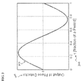
  • Fig 3 shows the output signal of the Gardner phase error detector 300 as a function of the phase error τ 302 expressed as fraction of a period. The curve 301 possesses a horizontal sinusoidal shape and is commonly termed s-curve. Its amplitude or its maximum derivation is termed by Gardner as "phase detector gain" KD indicating the performance quality.
  • The dynamic behavior of a clock recovery loop as shown in Fig. 2 depends among other parameters on the loop gain which is the product of all amplification factors in the loop, e.g. the loop filter gain Kp , the NCO gain K o (gain of the numerically controlled oscillator NCO 203), but also the implicit gain of the phase detector KD.
  • The problem is that the phase detector gain KD and thus the dynamic behavior of the loop depends on the input signal and especially on the distortions present in the input signal. This is undesirable since it makes the loop behavior difficult to analyze and predict.
  • As shown in J. W. M. Bergmans, "Digital Baseband Transmission and Recording", Kluwer, 1996 and in F. M. Gardner, "Phaselock Techniques", 2nd edition, Wiley, 1979, to characterize a second order Phase-Locked Loop PLL only the damping factor ζ and either the natural frequency ωn or the loop bandwidth BL have to be known. From these two parameters all other parameters can be derived: ω n T s = K f K D K 0 , ζ = 1 2 K D K 0 K p 2 K f , B L T S = ω n T S ζ + 1 4 ζ
    Figure imgb0001

    where the loop filter gain Kp is the amplification factor of the PI-filter in the proportional part and Kf is the amplification factor of the PI-filter in integral part (see Fig. 2), K o is the oscillator slope, KD is the phase detector slope and Ts is the symbol duration. The amplifications Kp, Kf and K o are fixed parameter, which will not change during transmission, whereas the parameter KD depends mainly on the pulse shape and the power of the received signal, but also on the distortions on the channel due to Differential Group Delay (DGD) and chromatic dispersion (CD). Due to these distortions, KD may vary depending on the transmission conditions. Therefore, it has to be distinguished between KD,design , which is used to design the PLL and KD,signal which results at the Phase Detector (PD) output after transmission. Simulations have shown that due to varying Differential Group Delay (DGD) on the channel the KD,signal at the Phase Detector (PD), output changes and this changes the loop gain of the whole PLL. The impact of changing KD,signal on the parameter of the PLL can be seen in Equation (2). It gives the effective parameters for the case that KD,design =xKD,signal · For KD,signal < KD,design the effective loop bandwidth BL,eff decreases due to the decreasing loop gain and vice versa. ζ eff = 1 x ζ design , ω n , eff = 1 x ω n , design , B L , eff = z B L , design
    Figure imgb0002

    with z = 1 + ζ design ζ design + 1 4 ζ design 1 x - 1
    Figure imgb0003
  • This behavior is a critical point in the design of the clock recovery. The clock recovery has to be stable during the whole transmission even if the loop gain changes. In general there are several limitations for the loop bandwidth BL,eff · The first one is the maximum symbol frequency offset which can be tracked. This limitation can be overcome by use of an active PI-filter which guarantees, in theory, that arbitrarily large symbol frequency offsets ΔfSym can be tracked. Thus, in terms of symbol frequency offset only the pull-in time is a criterion and the lower limit of the loop bandwidth is determined by the desired jitter tolerance. A further limitation is the additional delay in the loop.
  • As shown in J. W. M. Bergmans, "Effect of Loop Delay on Stability of Discrete-Time PLL", IEEE Trans. Circuits and Syst. I, Vol. 42, No. 4, pp.229-231, April 1995, the maximum loop bandwidth for a given additional loop delay of M symbols can be calculated as follows: B L , design T < 1 / 2 M design + 1 ζ design + 1 4 ζ design
    Figure imgb0004
  • If the effective loop bandwidth B L,eff increases, e.g. due to varying Differential Group Delay (DGD), the PLL may become unstable. The effective maximum tolerable additional loop delay of Meff symbols for KD,desgn = xKD,signal is : 2 M eff + 1 = 2 M design + 1 x
    Figure imgb0005
  • Conventional clock recovery designs as, for example, described in Fig. 2, usually assume a fully equalized and properly amplified input signal. Deviations of the input signal from these ideal conditions lead to a different than designed dynamic loop behaviour. The "solution" usually is to design the loop for the most probable scenario and restrict the input signal distortions to a limited range. If the distortions exceed this range, however, the loop may take longer than specified to reach the steady state and it may even become unstable and fail completely.
  • The problem to be solved is to overcome the disadvantages stated above and in particular to provide a solution that allows a stable loop behavior which can be adaptively adjustable.
  • SUMMARY OF THE INVENTION
  • This problem is solved according to the features of the independent claims. Further embodiments result from the depending claims.
  • In order to overcome this problem, a system comprising:
    • a clock recovery unit comprising a first phase detector unit;
    • an estimation unit comprising a second phase detector unit,
    • the estimation unit being configured to estimate the gain (KD ) of the second phase detector unit; wherein the estimation unit and the clock recovery unit are configured to operate in parallel.
  • In another embodiment, the estimated gain (KD ) of the second phase detector unit is configured to feed the first phase detector unit (402).
  • In a further embodiment, the system is configurable to achieve a constant loop gain
  • In a next embodiment the constant loop gain is configured to be adaptively adjustable.
  • In a further embodiment, the estimated gain (KD ) of the second phase detector unit comprises a variable part ( KD,Signal ) .
  • In another embodiment, the system is adjustable in such a way that the variable part (KD,slgnal) of the estimated gain (KD ) can be reduced to zero.
  • In a next embodiment, the clock recovery unit comprises a phase-locked-loop (PLL) system.
  • In a further embodiment, the phase-locked-loop (PLL) system includes a filter with perfect integrator (PI) path.
  • In a next embodiment, the first phase detector unit and the second phase detector unit are Gardner phase detectors.
  • In another embodiment, the system is a communication system.
  • In a next embodiment, the communication system is an optical communication system.
  • The problem stated above is further solved by a method of phase recovery for a system, the system comprising a clock recovery unit and an estimation unit, the clock recovery unit comprising a first phase detector unit and the estimation unit comprising second phase detector unit, the method comprising: estimating the gain of the second phase detector unit; wherein the estimation unit and the clock recovery unit operate in parallel.
  • In another embodiment, the method further comprises that the estimated gain (KD ) of the second phase detector unit feeds the first phase detector unit.
  • In a next embodiment, the method further comprises the step of adjusting the system so that a constant loop gain can be achieved.
  • In a further embodiment, the method further comprises that the constant loop gain is adaptively adjustable.
  • Particular properties and/or advantages of the approach provided may in particular be as follows:
    1. a. The influence of KD,signal on the dynamics of the PLL can be cancelled out.
    2. b. The loop behavior is stable and can be adaptively adjustable.
    BRIEF DESCRIPTION OF THE DRAWINGS
  • The invention is explained by way of example in more detail below with the aid of the attached drawings.
    • FIG 1 is a representation of a coherent receiver used in a conventional CP-QPSK optical communication system.
    • Fig 2 shows a conventional clock recovery arrangement
    • Fig 3 shows the output signal of the Gardner phase error detector as a function of the phase error τ expressed as fraction of a period.
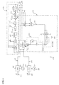
    • Fig 4 shows a clock recovery arrangement according to an embodiment of the invention.
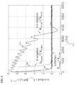
    • Fig 5 is an exemplary representation of the residual symbol frequency offset ΔfSym as a function of the time.
    • Fig 6 is an exemplary representation of the estimated loop bandwidth BL,eff.
    DESCRIPTION OF THE INVENTION
  • As regards the description of FIGs 1 to 3 , reference is made to the background of the invention.
  • Illustrative embodiments will now be described with reference to the accompanying drawings to disclose the teachings of the present invention. While the present invention is described herein with reference to illustrative embodiments for particular applications, it should be understood that the invention is not limited thereto. Those having ordinary skill in the art and access to the teachings provided herein will recognize additional modifications, applications, and embodiments within the scope thereof and additional fields in which the present invention would be of significant utility.
  • Fig 4 shows a clock recovery arrangement according to an embodiment of the invention, including a clock recovery unit (418) and an estimation unit (417), the clock recovery unit (418) including a first phase detector unit (402), and the estimation unit (417) including a second phase detector unit (419). The in-phase signal IX 405 is supplied to the first analog-to-digital converter (ADC) 406, which is fed by the clock 407 working at the frequency fADC, while the quadrature-phase signal QX 408 is supplied to the second analog-to-digital converter (ADC) 406, which is fed by the clock 407 working at the frequency fADC. The outputs 411 and 412 of the analog-to-digital converters (ADC) 406 and 410 are connected to an interpolation unit 404. The first output IXcorr(k) 413 and the second output QXcorr(k) 414 of the interpolation unit 404 are each supplied to a first Gardner Phase Detector (PD) 402. The output 415 of the first Gardner Phase Detector (PD) 402 is supplied to an active PI-filter 401 (i.e. filter with perfect integrator path) whose output 417 is connected to a Numerically Controlled Oscillator (NCO) 403. The output ε 416 of the Numerically Controlled Oscillator (NCO) 403 is fed to the interpolation unit 404.
  • The way in which the invention obtains a defined and stable loop behaviour is to estimate the phase detector gain in parallel to the clock recovery loop 418. Once this estimate has been obtained, it can be used to adjust a variable gain inside the loop in order to cancel out the variable part of the loop gain and achieve a constant overall loop gain which can be designed to be any favourable value.
  • In particular, before the clock recovery, an open loop configuration 417 is implemented which includes the same Phase Detector (PD) unit 419 as the one 402 included in the closed loop 418. The interpolator 404 can be omitted for this structure if a symbol frequency offset is considered, which may be the case in realistic setups. In this open loop configuration 417 first the s-curve is estimated by the Phase Detector (PD) unit 419 and from this estimation KD,signal is calculated by the KD,signal estimation unit 420. Moreover, the comparing unit 421 tests if the calculated KD,signal is zero. For the case that KD,sigal is zero, this parameter is set to a fixed value. The inverse of the calculated KD,signal is calculated by the inverting unit 422, and this value is multiplied with KD,design by the multiplying unit 423. For multiplication before the phase detector the square root is taken from this product by the square root unit 424. Afterwards this value is multiplied with the last estimated value by the multiplying unit 425 and then fed as an additional amplification or attenuation factor into the loop 418 and also into the open loop 417 as input to the first phase detector unit (402) and to the second phase detector unit (419). Due to this adaptive control the influence of KD,signal on the dynamics of the PLL is cancelled out. The speed of this adaptive control depends on the symbol frequency offset of the ADC. This offset determines the time, how long it takes to get a full s-curve, which is necessary to determine the actual KD,signal.
  • The approach described in the present invention can be used in any kind of loop where the loop behaviour depends on the distortions present in the input signal. In particular this applies to all control loops.
  • Fig 5 is an exemplary representation of the residual symbol frequency offset ΔfSym 51 as a function of the time 52 expressed in nanoseconds. The residual symbol frequency offset ΔfSym 51 is derived from the output of the integral part of the PI-filter 401, during the lock-in procedure for a 112 Gbit/s CP-QPSK transmission with an OSNR of 15 dB. For the curve 53 (with adaption) and the curve 54 (without adaption) it was assumed that KD,design =2KD,signal and for the curve 55 (reference) KD,design =KD,signal. The symbol frequency offset was set to ΔfSym = 10MHz, the damping factor was ζ = 0.707 and the loop bandwidth BL,design =10MHz . The curve 53 with adaptive control exhibits the same behavior after the time needed to calculate KD,signal (for this ΔfSym about 11200 samples ∼200 ns) as the reference system 55, whereas the system without adaptive control 54 requires a much longer pull-in and lock-in time, which implies a smaller loop bandwidth.
  • Fig 6 is an exemplary representation of the estimated loop bandwidth BL,eff 61 after the PI-filter 401 after lock-in of the PLL for the system without64 and with 63 adaptive control expressed as a function of the factor x=KD,design /KD,signal. Fig 6 shows that the estimated loop bandwidth of the system without adaptive control 64 has almost the same behaviour as the analytical curve 65 for the effective loop bandwidth BL,eff = ZBL,design (equation (2)). On the contrary the estimated loop bandwidth for the system with adaptive control 63 is the same for all values of x, which implies a constant loop gain and according to this a design of the digital PLL which is independent of KD,signal.
  • Abbreviations:
  • ADC
    Analogue-to-Digital Converter
    BER
    Bit Error Rate
    CD
    Chromatic Dispersion
    CP-QPSK
    Coherent Polarization Multiplexed Quaternary Phase-Shift Keying
    DGD
    Differential Group Delay
    DSP
    Digital Signal Processing
    PD
    Phase Detector
    QPSK
    Phase-locked loop
    PLL
    Cross Phase Modulation

Claims (15)

  1. A system (400) comprising:
    - a clock recovery unit (418) comprising a first phase detector unit (402);
    - an estimation unit (417) comprising a second phase detector unit (419), the estimation unit (417) being configured to estimate the gain (KD ) of the second phase detector unit (419);
    - wherein the estimation unit (417) and the clock recovery unit (418) are configured to operate in parallel.
  2. The system according to claim 1, wherein the estimated gain (KD ) of the second phase detector unit (419) is configured to feed the first phase detector unit (402).
  3. The system according to any of the preceding claims, wherein the system (400) is configurable to achieve a constant loop gain.
  4. The system according claim 3, wherein the constant loop gain is configured to be adaptively adjustable.
  5. The system according to any of the preceding claims, wherein the estimated gain (KD ) of the second phase detector unit (419) comprises a variable part (KD,signal ) .
  6. The system according claim 5, wherein the system (400) is adjustable in such a way that the variable part (KD,signal ) of the estimated gain (KD ) can be reduced to zero.
  7. The system according to any of the preceding claims, wherein the clock recovery unit (418) comprises a phase-locked-loop (PLL) system.
  8. The system according to claim 8 wherein the phase-locked-loop (PLL) system includes a filter with perfect integrator (PI) path (401).
  9. The system according any of the preceding claims wherein the first phase detector unit (402) and the second phase detector unit (419) are Gardner phase detectors.
  10. The system according any of the preceding claims wherein the system is a communication system.
  11. The system according to claim 10 wherein the communication system is an optical communication system.
  12. A method for phase recovery for a system (400), the system (400) comprising a clock recovery unit (418) and an estimation unit (417), the clock recovery unit (418) comprising a first phase detector unit (402) and the estimation unit (417) comprising second phase detector unit (419), the method comprising:
    - estimating the gain (KD ) of the second phase detector unit (419);
    - wherein the estimation unit (417) and the clock recovery unit (418) operate in parallel.
  13. The method according to claim 12 wherein the estimated gain (KD ) of the second phase detector unit (419) feeds the first phase detector unit (402).
  14. The method according to claim 12 or 13 further comprising: adjusting the system (400) so that a constant loop gain can be achieved.
  15. The method according to claim 14, wherein the constant loop gain is adaptively adjustable.
EP10177427A 2010-09-17 2010-09-17 Method and system for clock recovery with adaptive loop gain control Withdrawn EP2432128A1 (en)

Priority Applications (4)

Application Number Priority Date Filing Date Title
EP10177427A EP2432128A1 (en) 2010-09-17 2010-09-17 Method and system for clock recovery with adaptive loop gain control
EP11757332.9A EP2617134B1 (en) 2010-09-17 2011-09-16 Method and system for clock recovery with adaptive loop gain control
PCT/EP2011/066110 WO2012035142A1 (en) 2010-09-17 2011-09-16 Method and system for clock recovery with adaptive loop gain control
US13/824,551 US9436209B2 (en) 2010-09-17 2011-09-16 Method and system for clock recovery with adaptive loop gain control

Applications Claiming Priority (1)

Application Number Priority Date Filing Date Title
EP10177427A EP2432128A1 (en) 2010-09-17 2010-09-17 Method and system for clock recovery with adaptive loop gain control

Publications (1)

Publication Number Publication Date
EP2432128A1 true EP2432128A1 (en) 2012-03-21

Family

ID=43608880

Family Applications (2)

Application Number Title Priority Date Filing Date
EP10177427A Withdrawn EP2432128A1 (en) 2010-09-17 2010-09-17 Method and system for clock recovery with adaptive loop gain control
EP11757332.9A Active EP2617134B1 (en) 2010-09-17 2011-09-16 Method and system for clock recovery with adaptive loop gain control

Family Applications After (1)

Application Number Title Priority Date Filing Date
EP11757332.9A Active EP2617134B1 (en) 2010-09-17 2011-09-16 Method and system for clock recovery with adaptive loop gain control

Country Status (3)

Country Link
US (1) US9436209B2 (en)
EP (2) EP2432128A1 (en)
WO (1) WO2012035142A1 (en)

Families Citing this family (6)

* Cited by examiner, † Cited by third party
Publication number Priority date Publication date Assignee Title
KR20130049967A (en) * 2011-11-07 2013-05-15 한국전자통신연구원 Dpsk optical receiver
EP2634935B1 (en) * 2012-02-28 2014-09-17 Alcatel Lucent Coherent transponder with enhanced frequency locking
US9496965B2 (en) * 2014-08-15 2016-11-15 Alcatel-Lucent Usa Inc. Chromatic dispersion compensator with integrated anti-aliasing filter and resampler
US9806822B1 (en) 2016-07-07 2017-10-31 Elenion Technologies, Llc Coherent optical receiver testing
US11700008B2 (en) * 2021-01-22 2023-07-11 Rohde & Schwarz Gmbh & Co. Kg Phase-shifted sampling module and method for determining filter coefficients
KR20230123089A (en) * 2022-02-15 2023-08-23 삼성디스플레이 주식회사 Processor and electronic device including the same

Citations (3)

* Cited by examiner, † Cited by third party
Publication number Priority date Publication date Assignee Title
EP0926857A2 (en) * 1997-12-24 1999-06-30 Mitsubishi Denki Kabushiki Kaisha Data receiver having variable rate symbol timing recovery with non-synchronized sampling
US20020003847A1 (en) * 2000-07-06 2002-01-10 Matsushita Electric Industrial Co., Ltd. Clock recovery circuit
US20070092040A1 (en) * 2005-10-25 2007-04-26 Sony Corporation Synchronizing apparatus, synchronizing method, synchronizing program and data reproduction apparatus

Family Cites Families (3)

* Cited by examiner, † Cited by third party
Publication number Priority date Publication date Assignee Title
US6909331B2 (en) * 2002-08-28 2005-06-21 Qualcomm Incorporated Phase locked loop having a forward gain adaptation module
US7279857B2 (en) * 2003-08-27 2007-10-09 Hewlett-Packard Development Company, L.P. System, method, and computer-readable medium for reduction of commutation-related acoustic noise in a fan system
TW200721688A (en) * 2005-11-25 2007-06-01 Realtek Semiconductor Corp Phase lock circuit

Patent Citations (3)

* Cited by examiner, † Cited by third party
Publication number Priority date Publication date Assignee Title
EP0926857A2 (en) * 1997-12-24 1999-06-30 Mitsubishi Denki Kabushiki Kaisha Data receiver having variable rate symbol timing recovery with non-synchronized sampling
US20020003847A1 (en) * 2000-07-06 2002-01-10 Matsushita Electric Industrial Co., Ltd. Clock recovery circuit
US20070092040A1 (en) * 2005-10-25 2007-04-26 Sony Corporation Synchronizing apparatus, synchronizing method, synchronizing program and data reproduction apparatus

Non-Patent Citations (4)

* Cited by examiner, † Cited by third party
Title
F. M. GARDNER: "A BPSK/QPSK Timing-Error Detector for Sampled Receivers", IEEE TRANSACTIONS ON COMMUNICATIONS, vol. COM-34, no. 5, May 1986 (1986-05-01), pages 423 - 429
F. M. GARDNER: "Phaselock Techniques", 1979, WILEY
J. W. M. BERGMANS: "Digital Baseband Transmission and Recording", 1996, KLUWER
J. W. M. BERGMANS: "Effect of Loop Delay on Stability of Discrete-Time PLL", IEEE TRANS. CIRCUITS AND SYST. I, vol. 42, no. 4, April 1995 (1995-04-01), pages 229 - 231

Also Published As

Publication number Publication date
EP2617134A1 (en) 2013-07-24
US9436209B2 (en) 2016-09-06
US20140112424A1 (en) 2014-04-24
WO2012035142A1 (en) 2012-03-22
EP2617134B1 (en) 2020-01-01

Similar Documents

Publication Publication Date Title
EP2430788B1 (en) Phase detection method and phase detector
US8478137B2 (en) Optical receiver
US8909068B2 (en) Skew estimator, skew compensator and coherent receiver
EP2617134B1 (en) Method and system for clock recovery with adaptive loop gain control
US8358939B2 (en) Optical communication device
EP2375603A1 (en) Clock recovery method and clock recovery arrangement for coherent polarisation multiplex receivers
US20130070835A1 (en) Cdr with digitally controlled lock to reference
US20120148265A1 (en) Coherent optical receiving device capable of digital equalization of optical input, digital equalization method for optical input and coherent optical transmitting/receiving device
US20130181757A1 (en) Method and Device for Clock Recovery
US9906307B2 (en) Apparatus for characterizing a chromatic dispersion of an optical receive signal
EP3393096B1 (en) Receiving device
US8861648B2 (en) Receiving device and demodulation device
CN1961554B (en) Wireless communication device, demodulation method, and frequency deviation correction circuit
CN102369706B (en) Phase offset and jitter compensator
US5521939A (en) Timing reproduction device
US20030169837A1 (en) Timing recovery with variable bandwidth phase locked loop and non-linear control paths
WO2013110336A1 (en) Interference robust clock recovery
US9083498B2 (en) Method and device for processing data and communication system comprising such device
WO2017122605A1 (en) Digital signal processing circuit, and optical space communication system
JP2009081722A (en) Adaptive receiver
JP2010074506A (en) Clock regeneration circuit, demodulation circuit, receiving device, wireless communication system, and method of operating clock regeneration circuit
JPH0722294B2 (en) Automatic frequency control method
Hebebrand et al. Clock Recovery with DGD-tolerant Phase Detector for CP-QPSK Receivers

Legal Events

Date Code Title Description
PUAI Public reference made under article 153(3) epc to a published international application that has entered the european phase

Free format text: ORIGINAL CODE: 0009012

AK Designated contracting states

Kind code of ref document: A1

Designated state(s): AL AT BE BG CH CY CZ DE DK EE ES FI FR GB GR HR HU IE IS IT LI LT LU LV MC MK MT NL NO PL PT RO SE SI SK SM TR

AX Request for extension of the european patent

Extension state: BA ME RS

STAA Information on the status of an ep patent application or granted ep patent

Free format text: STATUS: THE APPLICATION IS DEEMED TO BE WITHDRAWN

18D Application deemed to be withdrawn

Effective date: 20120922