US12190845B2 - Processor and electronic device including the same - Google Patents
Processor and electronic device including the same Download PDFInfo
- Publication number
- US12190845B2 US12190845B2 US18/081,062 US202218081062A US12190845B2 US 12190845 B2 US12190845 B2 US 12190845B2 US 202218081062 A US202218081062 A US 202218081062A US 12190845 B2 US12190845 B2 US 12190845B2
- Authority
- US
- United States
- Prior art keywords
- clock
- buffer
- data
- buffers
- block
- Prior art date
- Legal status (The legal status is an assumption and is not a legal conclusion. Google has not performed a legal analysis and makes no representation as to the accuracy of the status listed.)
- Active, expires
Links
Images


Classifications
-
- G—PHYSICS
- G06—COMPUTING OR CALCULATING; COUNTING
- G06F—ELECTRIC DIGITAL DATA PROCESSING
- G06F1/00—Details not covered by groups G06F3/00 - G06F13/00 and G06F21/00
- G06F1/04—Generating or distributing clock signals or signals derived directly therefrom
- G06F1/06—Clock generators producing several clock signals
-
- G—PHYSICS
- G09—EDUCATION; CRYPTOGRAPHY; DISPLAY; ADVERTISING; SEALS
- G09G—ARRANGEMENTS OR CIRCUITS FOR CONTROL OF INDICATING DEVICES USING STATIC MEANS TO PRESENT VARIABLE INFORMATION
- G09G3/00—Control arrangements or circuits, of interest only in connection with visual indicators other than cathode-ray tubes
- G09G3/20—Control arrangements or circuits, of interest only in connection with visual indicators other than cathode-ray tubes for presentation of an assembly of a number of characters, e.g. a page, by composing the assembly by combination of individual elements arranged in a matrix no fixed position being assigned to or needed to be assigned to the individual characters or partial characters
- G09G3/2092—Details of a display terminals using a flat panel, the details relating to the control arrangement of the display terminal and to the interfaces thereto
- G09G3/2096—Details of the interface to the display terminal specific for a flat panel
-
- G—PHYSICS
- G06—COMPUTING OR CALCULATING; COUNTING
- G06F—ELECTRIC DIGITAL DATA PROCESSING
- G06F1/00—Details not covered by groups G06F3/00 - G06F13/00 and G06F21/00
- G06F1/26—Power supply means, e.g. regulation thereof
- G06F1/32—Means for saving power
- G06F1/3203—Power management, i.e. event-based initiation of a power-saving mode
- G06F1/3234—Power saving characterised by the action undertaken
- G06F1/3287—Power saving characterised by the action undertaken by switching off individual functional units in the computer system
-
- G—PHYSICS
- G09—EDUCATION; CRYPTOGRAPHY; DISPLAY; ADVERTISING; SEALS
- G09G—ARRANGEMENTS OR CIRCUITS FOR CONTROL OF INDICATING DEVICES USING STATIC MEANS TO PRESENT VARIABLE INFORMATION
- G09G3/00—Control arrangements or circuits, of interest only in connection with visual indicators other than cathode-ray tubes
- G09G3/20—Control arrangements or circuits, of interest only in connection with visual indicators other than cathode-ray tubes for presentation of an assembly of a number of characters, e.g. a page, by composing the assembly by combination of individual elements arranged in a matrix no fixed position being assigned to or needed to be assigned to the individual characters or partial characters
- G09G3/22—Control arrangements or circuits, of interest only in connection with visual indicators other than cathode-ray tubes for presentation of an assembly of a number of characters, e.g. a page, by composing the assembly by combination of individual elements arranged in a matrix no fixed position being assigned to or needed to be assigned to the individual characters or partial characters using controlled light sources
- G09G3/30—Control arrangements or circuits, of interest only in connection with visual indicators other than cathode-ray tubes for presentation of an assembly of a number of characters, e.g. a page, by composing the assembly by combination of individual elements arranged in a matrix no fixed position being assigned to or needed to be assigned to the individual characters or partial characters using controlled light sources using electroluminescent panels
- G09G3/32—Control arrangements or circuits, of interest only in connection with visual indicators other than cathode-ray tubes for presentation of an assembly of a number of characters, e.g. a page, by composing the assembly by combination of individual elements arranged in a matrix no fixed position being assigned to or needed to be assigned to the individual characters or partial characters using controlled light sources using electroluminescent panels semiconductive, e.g. using light-emitting diodes [LED]
-
- G—PHYSICS
- G09—EDUCATION; CRYPTOGRAPHY; DISPLAY; ADVERTISING; SEALS
- G09G—ARRANGEMENTS OR CIRCUITS FOR CONTROL OF INDICATING DEVICES USING STATIC MEANS TO PRESENT VARIABLE INFORMATION
- G09G5/00—Control arrangements or circuits for visual indicators common to cathode-ray tube indicators and other visual indicators
- G09G5/003—Details of a display terminal, the details relating to the control arrangement of the display terminal and to the interfaces thereto
- G09G5/006—Details of the interface to the display terminal
- G09G5/008—Clock recovery
-
- G—PHYSICS
- G09—EDUCATION; CRYPTOGRAPHY; DISPLAY; ADVERTISING; SEALS
- G09G—ARRANGEMENTS OR CIRCUITS FOR CONTROL OF INDICATING DEVICES USING STATIC MEANS TO PRESENT VARIABLE INFORMATION
- G09G2310/00—Command of the display device
- G09G2310/02—Addressing, scanning or driving the display screen or processing steps related thereto
- G09G2310/0243—Details of the generation of driving signals
-
- G—PHYSICS
- G09—EDUCATION; CRYPTOGRAPHY; DISPLAY; ADVERTISING; SEALS
- G09G—ARRANGEMENTS OR CIRCUITS FOR CONTROL OF INDICATING DEVICES USING STATIC MEANS TO PRESENT VARIABLE INFORMATION
- G09G2310/00—Command of the display device
- G09G2310/02—Addressing, scanning or driving the display screen or processing steps related thereto
- G09G2310/0264—Details of driving circuits
- G09G2310/0291—Details of output amplifiers or buffers arranged for use in a driving circuit
-
- G—PHYSICS
- G09—EDUCATION; CRYPTOGRAPHY; DISPLAY; ADVERTISING; SEALS
- G09G—ARRANGEMENTS OR CIRCUITS FOR CONTROL OF INDICATING DEVICES USING STATIC MEANS TO PRESENT VARIABLE INFORMATION
- G09G2330/00—Aspects of power supply; Aspects of display protection and defect management
- G09G2330/02—Details of power systems and of start or stop of display operation
- G09G2330/021—Power management, e.g. power saving
-
- G—PHYSICS
- G09—EDUCATION; CRYPTOGRAPHY; DISPLAY; ADVERTISING; SEALS
- G09G—ARRANGEMENTS OR CIRCUITS FOR CONTROL OF INDICATING DEVICES USING STATIC MEANS TO PRESENT VARIABLE INFORMATION
- G09G2370/00—Aspects of data communication
- G09G2370/08—Details of image data interface between the display device controller and the data line driver circuit
-
- Y—GENERAL TAGGING OF NEW TECHNOLOGICAL DEVELOPMENTS; GENERAL TAGGING OF CROSS-SECTIONAL TECHNOLOGIES SPANNING OVER SEVERAL SECTIONS OF THE IPC; TECHNICAL SUBJECTS COVERED BY FORMER USPC CROSS-REFERENCE ART COLLECTIONS [XRACs] AND DIGESTS
- Y02—TECHNOLOGIES OR APPLICATIONS FOR MITIGATION OR ADAPTATION AGAINST CLIMATE CHANGE
- Y02D—CLIMATE CHANGE MITIGATION TECHNOLOGIES IN INFORMATION AND COMMUNICATION TECHNOLOGIES [ICT], I.E. INFORMATION AND COMMUNICATION TECHNOLOGIES AIMING AT THE REDUCTION OF THEIR OWN ENERGY USE
- Y02D10/00—Energy efficient computing, e.g. low power processors, power management or thermal management
Definitions
- Embodiments of the disclosure described herein relate to a processor with reduced power consumption and an electronic device including the processor.
- An electronic device may include a host processor, a driving driver, and a display panel.
- the host processor may transmit input image data to the driving driver, and the driving driver may generate a data signal based on the input image data.
- the host processor and the driving driver may be connected to each other through a predetermined interface.
- the host processor includes a data transmitter, and frame data (or commands) may be transmitted from the host processor to the driving driver.
- Embodiments of the disclosure provide a processor with reduced power consumption and an electronic device including the processor.
- an electronic device includes a host processor including a data transmitter, a driving driver which is connected to the host processor in an interface mode and receives data from the host processor, and a display panel which is controlled by the driving driver.
- the data transmitter includes a phase locked loop which generates a first clock and a second clock, a clock block which receives the first clock and output a clock signal to a clock lane, a plurality of data blocks which receive the second clock and respectively output serial data to a plurality of data lanes, a first buffer connected between the phase locked loop and the clock block, and a plurality of second buffers respectively connected between the phase locked loop and the plurality of data blocks, and the first buffer and each of the plurality of second buffers are activated or deactivated depending on the interface mode.
- the data transmitter may further include a voltage regulator which generates a voltage provided to the clock block and the plurality of data blocks, a third buffer connected between the voltage regulator and the clock block, and a plurality of fourth buffers respectively connected between the voltage regulator and the plurality of data blocks, and the third buffer and each of the plurality of fourth buffers may be activated or deactivated depending on the interface mode.
- a voltage regulator which generates a voltage provided to the clock block and the plurality of data blocks
- a third buffer connected between the voltage regulator and the clock block
- a plurality of fourth buffers respectively connected between the voltage regulator and the plurality of data blocks
- the first buffer, the plurality of second buffers, the third buffer, and the plurality of fourth buffers may be all activated.
- the first buffer and the third buffer may be deactivated, at least one second buffer of the plurality of second buffers may be activated and the remaining second buffers of the plurality of second buffers may be deactivated, and at least one fourth buffer of the plurality of fourth buffers may be activated and the remaining fourth buffers of the plurality of fourth buffers may be deactivated.
- both the clock lane and the plurality of data lanes may be used, and in the second interface mode, at least one data lane selected from the clock lane and the plurality of data lanes may be used.
- the plurality of data blocks may include a first data block, a second data block, a third data block, and a fourth data block.
- the plurality of second buffers may include a first clock buffer connected between the first data block and the phase locked loop, a second clock buffer connected between the second data block and the phase locked loop, a third clock buffer connected between the third data block and the phase locked loop, and a fourth clock buffer connected between the fourth data block and the phase locked loop.
- the plurality of fourth buffers may include a first voltage buffer connected between the first data block and the voltage regulator, a second voltage buffer connected between the second data block and the voltage regulator, a third voltage buffer connected between the third data block and the voltage regulator, and a fourth voltage buffer connected between the fourth data block and the voltage regulator.
- the first clock buffer and the first voltage buffer may be activated, and the second clock buffer, the third clock buffer, the fourth clock buffer, the second voltage buffer, the third voltage buffer, and the fourth voltage buffer may be deactivated.
- the first clock buffer, the second clock buffer, the first voltage buffer, and the second voltage buffer may be activated, and the third clock buffer, the fourth clock buffer, the third voltage buffer, and the fourth voltage buffer may be deactivated.
- the electronic device may further include a signal generator which generates control signals for controlling each of operations of the first buffer, the plurality of second buffers, the third buffer, and the plurality of fourth buffers depending on the interface mode.
- a distance between an input terminal of the first buffer and an output terminal of the phase locked loop may be less than a distance between an output terminal of the first buffer and an input terminal of the clock block.
- a distance between an input terminal of each of the plurality of second buffers and an output terminal of the phase locked loop may be less than each of distances between output terminals of the plurality of second buffers and input terminals of the plurality of data blocks.
- the clock block and each of the plurality of data blocks may include a clock divider which divides the first clock or the second clock by an integer multiple, a digital processor which receives a signal from the clock divider and digitally processes the signal, a low power driver which processes data received from the digital processor and outputs a signal to the clock lane or the plurality of data lanes when the data transmitter operates in a low power mode, a serial converter which converts the data received from the digital processor into serial data when the data transmitter operates in a high-speed mode, and a high-speed driver which processes the serial data received from the serial converter to output a signal to the clock lane or the plurality of data lanes when the data transmitter operates in the high-speed mode.
- a clock divider which divides the first clock or the second clock by an integer multiple
- a digital processor which receives a signal from the clock divider and digitally processes the signal
- a low power driver which processes data received from the digital processor and outputs a signal to the clock lane or the plurality of data la
- the processor may include a data transmitter which outputs data through a predetermined interface mode.
- the data transmitter includes a phase locked loop which generates a first clock and a second clock, a clock block which receives the first clock and output a clock signal to a clock lane, a plurality of data blocks which receives the second clock and respectively outputs serial data to a plurality of data lanes, a first buffer connected between the phase locked loop and the clock block, and a plurality of second buffers respectively connected between the phase locked loop and the plurality of data blocks, and the first buffer and each of the plurality of second buffers are activated or deactivated depending on the interface mode.
- the data transmitter may further include a voltage regulator which generates a voltage provided to the clock block and the plurality of data blocks, a third buffer connected between the voltage regulator and the clock block, and a plurality of fourth buffers respectively connected between the voltage regulator and the plurality of data blocks, and the third buffer and each of the plurality of fourth buffers may be activated or deactivated depending on the interface mode.
- a voltage regulator which generates a voltage provided to the clock block and the plurality of data blocks
- a third buffer connected between the voltage regulator and the clock block
- a plurality of fourth buffers respectively connected between the voltage regulator and the plurality of data blocks
- the first buffer, the plurality of second buffers, the third buffer, and the plurality of fourth buffers may be all activated.
- the first buffer and the third buffer may be deactivated, at least one second buffer of the plurality of second buffers may be activated and the remaining second buffers of the plurality of second buffers may be deactivated, and at least one fourth buffer of the plurality of fourth buffers may be activated and the remaining fourth buffers of the plurality of fourth buffers may be deactivated.
- the processor may further include a signal generator which generates control signals for controlling each of operations of the first buffer, the plurality of second buffers, the third buffer, and the plurality of fourth buffers depending on the interface mode.
- a distance between an input terminal of the first buffer and an output terminal of the phase locked loop may be less than a distance between an output terminal of the first buffer and an input terminal of the clock block.
- a distance between an input terminal of each of the plurality of second buffers and an output terminal of the phase locked loop may be less than each of distances between output terminals of the plurality of second buffers and input terminals of the plurality of data blocks.
- the clock block and each of the plurality of data blocks may include a clock divider which divides the first clock or the second clock by an integer multiple, a digital processor which receives a signal from the clock divider and digitally processes the signal, a low power driver which processes data received from the digital processor and outputs a signal to the clock lane or the plurality of data lanes when the data transmitter operates in a low power mode, a serial converter which converts the data received from the digital processor into serial data when the data transmitter operates in a high-speed mode, and a high-speed driver which processes the serial data received from the serial converter to output a signal to the clock lane or the plurality of data lanes when the data transmitter operates in the high-speed mode.
- a clock divider which divides the first clock or the second clock by an integer multiple
- a digital processor which receives a signal from the clock divider and digitally processes the signal
- a low power driver which processes data received from the digital processor and outputs a signal to the clock lane or the plurality of data la
- FIG. 1 is a block diagram of an electronic device according to an embodiment of the disclosure
- FIG. 2 is a block diagram of a data transmitter according to an embodiment of the disclosure
- FIG. 3 is a block diagram illustrating a data transmitter and a data receiver connected in a first interface mode, according to an embodiment of the disclosure
- FIG. 4 A is a block diagram illustrating a data transmitter and a data receiver connected in a second interface mode, according to an embodiment of the disclosure.
- FIG. 4 B is a block diagram of a data transmitter illustrated in FIG. 4 A ;
- FIG. 5 A is a block diagram illustrating a data transmitter and a data receiver connected in a second interface mode, according to an embodiment of the disclosure
- FIG. 5 B is a block diagram of a data transmitter illustrated in FIG. 5 A ;
- FIG. 6 is a block diagram of a clock block, according to an embodiment of the disclosure.
- FIG. 7 is a block diagram of a data block, according to an embodiment of the disclosure.
- first”, “second”, etc. are used to describe various components, but the components are not limited by the terms. The terms are used only to differentiate one component from another component. For example, a first component may be named as a second component, and vice versa, without departing from the spirit or scope of the disclosure.
- the terms “part” and “unit” mean a software component or a hardware component that performs a specific function.
- the hardware component may include, for example, a field-programmable gate array (FPGA) or an application-specific integrated circuit (ASIC).
- the software component may refer to executable code and/or data used by executable code in an addressable storage medium.
- software components may be, for example, object-oriented software components, class components, and working components, and may include processes, functions, properties, procedures, subroutines, program code segments, drivers, firmware, micro-codes, circuits, data, databases, data structures, tables, arrays or variables.
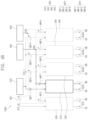
- FIG. 1 is a block diagram of an electronic device according to an embodiment of the disclosure.
- an embodiment of an electronic device ED may include a host processor HP (or a processor), a driving driver DVD, and a display panel DP.
- the electronic device ED may further include a memory, a camera, and various sensors in addition to the configuration illustrated in FIG. 1 .
- the electronic device ED may be a device activated depending on an electrical signal.
- the electronic device ED may process image data and may display the processed image data through the display panel DP.
- the electronic device ED may be a mobile phone, a tablet, a car navigation system, a game console, or a wearable device, but is not limited thereto.
- the host processor HP may be implemented with an integrated circuit, a system on a chip, an application processor, or a mobile application processor, but is not particularly limited thereto.
- the host processor HP may control various components included in the electronic device ED, for example, the driving driver DVD.
- the host processor HP may include a data transmitter 1000 .
- the data transmitter 1000 may operate in a way such that undesired clocks and voltages are not provided to blocks that are deactivated according to an interface mode. Accordingly, the host processor HP capable of being universally applicable to various interfaces and having reduced power consumption may be provided. This will be more fully detailed later.
- the driving driver DVD may control the display panel DP.
- the driving driver DVD may include a data receiver 2000 .
- the driving driver DVD may be connected to the host processor HP in a predetermined interface mode.
- the driving driver DVD may receive data, for example, an input image signal and a control signal from the host processor HP, and may generate an output image signal obtained by converting a data format to meet the interface specification of the display panel DP.
- the driving driver DVD may provide a scan driving signal, a data driving signal, and an output image signal to the display panel DP.
- the display panel DP may be configured to actually generate an image.
- the display panel DP may include a plurality of pixels, and is controlled by the driving driver DVD to display an image.
- the display panel DP may be a light emitting display panel, for example, the display panel DP may be an organic light emitting display panel, an inorganic light emitting display panel, an organic-inorganic light emitting display panel, a quantum dot display panel, a micro LED display panel, or a nano LED display panel, but is not particularly limited thereto.
- FIG. 2 is a block diagram of a data transmitter according to an embodiment of the disclosure.
- an embodiment of the data transmitter 1000 may include a phase locked loop 100 , a clock block 200 , a plurality of data blocks 300 , a voltage regulator 400 , and a signal generator 500 .
- the data transmitter 1000 may further include configurations for the operation of the data transmitter 1000 .
- the data transmitter 1000 may further include a bias circuit that generates a current.
- the phase locked loop 100 may generate a first clock CLK_Q and a second clock CLK_I.
- a first buffer BF 1 and a plurality of second buffers BF 2 may be connected to an output terminal of the phase locked loop 100 .
- the first buffer BF 1 and the second buffers BF 2 may be configured to be selectively activated or deactivated.
- clock gating may be applied to the first buffer BF 1 and each of the second buffers BF 2 .
- the first clock CLK_Q and the second clock CLK_I may be provided only to used blocks among the clock block 200 and the plurality of data blocks 300 .
- the clock block 200 may receive the first clock CLK_Q and may output a clock signal to a clock lane CLN.
- the clock lane CLN may include two transmission lines CA and CB.
- the plurality of data blocks 300 may include a first data block 310 , a second data block 320 , a third data block 330 , and a fourth data block 340 .
- Each of the first to fourth data blocks 310 , 320 , 330 , and 340 may receive the second clock CLK_I and may output serial data to first to fourth data lanes DLN 1 , DLN 2 , DLN 3 , and DLN 4 , respectively.
- Each of the first to fourth data lanes DLN 1 , DLN 2 , DLN 3 , and DLN 4 may include two transmission lines DA and DB.
- Each of the plurality of data blocks 300 may operate in a high-speed (HS) mode or a low-power (LP) mode.
- HS high-speed
- LP low-power
- differential signals may be transmitted through two transmission lines DA and DB.
- a single output signal may be transmitted through two transmission lines DA and DB.
- this is only an example and is not particularly limited thereto.
- the voltage regulator 400 may generate a voltage HSV to be provided to the clock block 200 and the plurality of data blocks 300 .
- the voltage regulator 400 may generate the voltage HSV used for operating in the high-speed mode and may transmit the voltage HSV to the clock block 200 and the plurality of data blocks 300 .
- a third buffer BF 3 and a plurality of fourth buffers BF 4 may be connected to an output terminal of the voltage regulator 400 .
- the third buffer BF 3 and the plurality of fourth buffers BF 4 may be configured to be selectively activated or deactivated.
- clock gating may be applied to the third buffer BF 3 and each of the fourth buffers BF 4 . Accordingly, the voltage HSV may be provided only to used blocks among the clock block 200 and the plurality of data blocks 300 .
- a distance (or a length of line connected) between an input terminal of the first buffer BF 1 and an output terminal of the phase locked loop 100 may be less than a distance between an output terminal of the first buffer BF 1 and an input terminal of the clock block 200 .
- the first buffer BF 1 may be disposed as close to the phase locked loop 100 as possible. In such an embodiment, a loading of a path through which the first clock CLK_Q is transmitted may be minimized.
- the distances may be identified through a layout of the data transmitter 1000 .
- FIG. 2 is a block diagram representing the distance relationship in terms of the length of a line.
- a distance between an input terminal of each of the plurality of second buffers BF 2 and the output terminal of the phase locked loop 100 may be less than each of the distances between output terminals of the plurality of second buffers BF 2 and input terminals of the plurality of data blocks 300 .
- each of the plurality of second buffers BF 2 may be disposed as close to the phase locked loop 100 as possible. In such an embodiment, a loading of a path through which the second clock CLK_I is transmitted may be minimized.
- the plurality of second buffers BF 2 may include a first clock buffer CBF 1 connected between the first data block 310 and the phase locked loop 100 , a second clock buffer CBF 2 connected between the second data block 320 and the phase locked loop 100 , a third clock buffer CBF 3 connected between the third data block 330 and the phase locked loop 100 , and a fourth clock buffer CBF 4 connected between the fourth data block 340 and the phase locked loop 100 .
- the plurality of fourth buffers BF 4 may include a first voltage buffer VBF 1 connected between the first data block 310 and the voltage regulator 400 , a second voltage buffer VBF 2 connected between the second data block 320 and the voltage regulator 400 , a third voltage buffer VBF 3 connected between the third data block 330 and the voltage regulator 400 , and a fourth voltage buffer VBF 4 connected between the fourth data block 340 and the voltage regulator 400 .
- the signal generator 500 may generate control signals CSG for controlling each of operations of the first buffer BF 1 , the first to fourth clock buffers CBF 1 , CBF 2 , CBF 3 , and CBF 4 , the third buffer BF 3 , and the first to fourth voltage buffers VBF 1 , VBF 2 , VBF 3 , and VBF 4 depending on an interface mode.
- FIG. 3 is a block diagram illustrating a data transmitter and a data receiver connected in a first interface mode, according to an embodiment of the disclosure.
- FIG. 3 illustrates lanes that are used in a first interface mode.
- all of the clock lane CLN and the first to fourth data lanes DLN 1 , DLN 2 , DLN 3 , and DLN 4 may be used.
- both the clock block 200 and the plurality of data blocks 300 may be activated.
- the signal generator 500 may generate the control signals CSG such that the first buffer BF 1 , the first to fourth clock buffers CBF 1 , CBF 2 , CBF 3 , and CBF 4 , the third buffer BF 3 , and the first to fourth voltage buffers VBF 1 , VBF 2 , VBF 3 , and VBF 4 may be all activated.
- the clock block 200 may receive the first clock CLK_Q from the phase locked loop 100 and the voltage HSV from the voltage regulator 400 .
- each of the first to fourth data blocks 310 , 320 , 330 , and 340 may receive the second clock CLK_I from the phase locked loop 100 and may receive the voltage HSV from the voltage regulator 400 .
- FIG. 4 A is a block diagram illustrating a data transmitter and a data receiver connected in a second interface mode, according to an embodiment of the disclosure.
- FIG. 4 B is a block diagram of a data transmitter illustrated in FIG. 4 A .
- a data transfer rate in the second interface mode may be faster than a data transfer rate in the first interface mode.
- the data transfer rate in the second interface mode may be 6 Gbps.
- the electronic device ED (refer to FIG. 1 ) is communicating in the second interface mode
- at least some of the clock block 200 and the plurality of data blocks 310 , 320 , 330 , and 340 of the host processor HP are deactivated.
- the clock lane CLN and the second to fourth data lanes DLN 2 , LN 3 , and DLN 4 may not be used.
- the signal generator 500 may generate the control signals CSG in a way such that the first buffer BF 1 , the second to fourth clock buffers CBF 2 , CBF 3 , and CBF 4 , the third buffer BF 3 , and the second to fourth voltage buffers VBF 2 , VBF 3 , and VBF 4 may be deactivated, and the first clock buffer CBF 1 and the first voltage buffer VBF 1 may be activated. Accordingly, in the second interface mode, the first clock CLK_Q and the voltage HSV may not be provided to the deactivated clock block 200 , and the second clock CLK_I and voltage HSV may not be provided to the deactivated second to fourth data blocks 320 , 330 , and 340 .
- the clock block 200 and the second to fourth data blocks 320 , 330 , and 340 may be blocked. Accordingly, since the first and second clocks CLK_Q and CLK_I are not applied to the clock block 200 and the second to fourth data blocks 320 , 330 , and 340 , which are not used, undesired dynamic power consumption may decrease.
- FIG. 5 A is a block diagram illustrating a data transmitter and a data receiver connected in a second interface mode, according to an embodiment of the disclosure.
- FIG. 5 B is a block diagram of a data transmitter illustrated in FIG. 5 A .
- a second interface mode illustrated in FIGS. 5 A and 5 B may be actually the same as the second interface mode illustrated in FIGS. 4 A and 4 B .
- the second data block 320 may be additionally activated.
- the second data block 320 may be additionally activated as the data transfer rate in the second interface mode illustrated in FIGS. 5 A and 5 B is less than the data transfer rate in the second interface mode illustrated in FIGS. 4 A and 4 B .
- the signal generator 500 may generate the control signals CSG in a way such that the first buffer BF 1 , the third and fourth clock buffers CBF 3 and CBF 4 , the third buffer BF 3 , and the third and fourth voltage buffers VBF 3 and VBF 4 are deactivated, and the first and second clock buffers CBF 1 and CBF 2 and the first and second voltage buffers VBF 1 and VBF 2 are activated.
- the first clock CLK_Q and the voltage HSV may not be provided to the deactivated clock block 200
- the second clock CLK_I and voltage HSV may not be provided to the deactivated second to fourth data blocks 320 , 330 , and 340 .
- FIG. 6 is a block diagram of a clock block, according to an embodiment of the disclosure.
- an embodiment of the clock block 200 may include a clock divider 201 , a digital processor 202 , low-power drivers 203 LX 1 and 203 LX 2 , a serial converter 204 , and a high-speed driver 205 HS.
- the clock block 200 illustrated in FIG. 6 is only an example, and the disclosure is not particularly limited thereto.
- the clock block 200 may be variously modified as long as the clock block 200 is configured to receive the first clock CLK_Q to generate a predetermined clock signal, and to transmit the predetermined clock signal through the clock lane CLN.
- the clock divider 201 may divide the first clock CLK_Q by an integer multiple. In an embodiment, for example, the clock divider 201 may divide the first clock CLK_Q by 1/16, but is not particularly limited thereto.
- the digital processor 202 may receive a signal from the clock divider 201 and digitally process the received signal. In an embodiment, for example, the digital processor 202 may process a clock signal for representing an image. In an embodiment, for example, the digital processor 202 may transmit a plurality of bits per one clock in the form of a bus. The plurality of bits may be, for example, 16 bits or 32 bits, but is not particularly limited thereto.
- the low-power drivers 203 LX 1 and 203 LX 2 may process the data received from the digital processor 202 and output a clock signal to the clock lane CLN when the data transmitter 1000 (refer to FIG. 1 ) operates in the low-power mode.
- the low-power drivers 203 LX 1 and 203 LX 2 may include a first low-power driver 203 LX 1 and a second low-power driver 203 LX 2 , the first low-power driver 203 LX 1 may output a signal through one transmission line CA, and the second low-power driver 203 LX 2 may output a signal to the other transmission line CB.
- the serial converter 204 may convert data received from the digital processor 202 into serial data.
- the high-speed driver 205 HS may receive the voltage HSV from the voltage regulator 400 (refer to FIG. 2 ).
- the high-speed driver 205 HS may process serial data received from the serial converter 204 and may output the processed serial data to the clock lane CLN.
- the high-speed driver 205 HS may output differential signals through the two transmission lines CA and CB.
- FIG. 7 is a block diagram of a data block, according to an embodiment of the disclosure.
- the data block 300 may include a clock divider 301 , a digital processor 302 , low-power drivers 303 LX 1 and 303 LX 2 , a serial converter 304 , and a high-speed driver 305 HS.
- the data block 300 illustrated in FIG. 7 is only an example, and the disclosure is not particularly limited thereto.
- the data block 300 may be variously modified as long as the data block 300 is configured to receive predetermined data to convert the predetermined data into serial data, and to transmit the serial data through the data lane DLN.
- the data block 300 may further include a low-power connection detector and a low-power receiver.
- the clock divider 301 may divide the second clock CLK_I by an integer multiple. In an embodiment, for example, the clock divider 301 may divide the second clock CLK_I by 1/16, but is not particularly limited thereto.
- the digital processor 302 may receive a signal from the clock divider 301 and digitally process the received signal. In an embodiment, for example, the digital processor 302 may process data for representing an image. In an embodiment, for example, the digital processor 302 may transmit a plurality of bits per one clock in the form of a BUS. The plurality of bits may be, for example, 16 bits or 32 bits, but is not particularly limited thereto.
- the low-power drivers 303 LX 1 and 303 LX 2 may process the data received from the digital processor 302 and may output a signal to the data lane DLN when the data transmitter 1000 (refer to FIG. 1 ) operates in the low-power mode.
- the low-power drivers 303 LX 1 and 303 LX 2 may include a first low-power driver 303 LX 1 and a second low-power driver 303 LX 2 , the first low-power driver 303 LX 1 may output a signal through one transmission line DA, and the second low-power driver 303 LX 2 may output a signal to the other transmission line DB.
- the serial converter 304 may convert data received from the digital processor 302 into serial data.
- the high-speed driver 305 HS may receive the voltage HSV from the voltage regulator 400 (refer to FIG. 2 ).
- the high-speed driver 305 HS may process serial data received from the serial converter 304 and may output the processed serial data to the data lane DLN.
- the high-speed driver 305 HS may output differential signals through the two transmission lines DA and DB.
- a path through which a clock or voltage is provided to unused blocks in a specific interface mode may be blocked. Accordingly, as power consumption by unused blocks is removed or reduced, power consumption of the electronic device may be reduced.
Landscapes
- Engineering & Computer Science (AREA)
- Theoretical Computer Science (AREA)
- Physics & Mathematics (AREA)
- General Physics & Mathematics (AREA)
- Computer Hardware Design (AREA)
- General Engineering & Computer Science (AREA)
- Computing Systems (AREA)
- Dc Digital Transmission (AREA)
- Information Transfer Systems (AREA)
- Power Sources (AREA)
- Synchronisation In Digital Transmission Systems (AREA)
Abstract
Description
Claims (20)
Applications Claiming Priority (2)
| Application Number | Priority Date | Filing Date | Title |
|---|---|---|---|
| KR10-2022-0019608 | 2022-02-15 | ||
| KR1020220019608A KR20230123089A (en) | 2022-02-15 | 2022-02-15 | Processor and electronic device including the same |
Publications (2)
| Publication Number | Publication Date |
|---|---|
| US20230260479A1 US20230260479A1 (en) | 2023-08-17 |
| US12190845B2 true US12190845B2 (en) | 2025-01-07 |
Family
ID=87558981
Family Applications (1)
| Application Number | Title | Priority Date | Filing Date |
|---|---|---|---|
| US18/081,062 Active 2043-01-13 US12190845B2 (en) | 2022-02-15 | 2022-12-14 | Processor and electronic device including the same |
Country Status (3)
| Country | Link |
|---|---|
| US (1) | US12190845B2 (en) |
| KR (1) | KR20230123089A (en) |
| CN (1) | CN116610188A (en) |
Citations (11)
| Publication number | Priority date | Publication date | Assignee | Title |
|---|---|---|---|---|
| US7137591B2 (en) * | 2003-02-19 | 2006-11-21 | Cartercopters, L.L.C. | Tilting mast in a rotorcraft |
| US7197591B2 (en) | 2004-06-30 | 2007-03-27 | Intel Corporation | Dynamic lane, voltage and frequency adjustment for serial interconnect |
| US20090324215A1 (en) * | 2008-06-30 | 2009-12-31 | Huawei Technologies Co., Ltd. | Active/standby switchover method and device of asynchronous backplane in transport network |
| US9141162B2 (en) | 2012-10-05 | 2015-09-22 | Intel Corporation | Apparatus, system and method for gated power delivery to an I/O interface |
| US20160218724A1 (en) * | 2015-01-22 | 2016-07-28 | Wright State University | High performance phase frequency detectors |
| US9436209B2 (en) * | 2010-09-17 | 2016-09-06 | Xieon Networks S.A.R.L. | Method and system for clock recovery with adaptive loop gain control |
| US20170220517A1 (en) * | 2016-02-01 | 2017-08-03 | Qualcomm Incorporated | Unidirectional clock signaling in a high-speed serial link |
| US9805687B2 (en) | 2014-09-03 | 2017-10-31 | Samsung Display Co., Ltd. | Display driver integrated circuit, display module and display system including the same |
| US10014862B2 (en) | 2015-06-22 | 2018-07-03 | Samsung Electronics Co., Ltd. | Clock gating circuit operates at high speed |
| JP2021136603A (en) | 2020-02-27 | 2021-09-13 | キヤノン株式会社 | Imaging device and its control method and program |
| US20220043161A1 (en) * | 2018-12-21 | 2022-02-10 | Nikolai Tcherniakovski | Multichannel multisystem radio-frequency unit of navigational satellite receiver |
-
2022
- 2022-02-15 KR KR1020220019608A patent/KR20230123089A/en active Pending
- 2022-12-14 US US18/081,062 patent/US12190845B2/en active Active
-
2023
- 2023-01-31 CN CN202310046280.9A patent/CN116610188A/en active Pending
Patent Citations (14)
| Publication number | Priority date | Publication date | Assignee | Title |
|---|---|---|---|---|
| US7137591B2 (en) * | 2003-02-19 | 2006-11-21 | Cartercopters, L.L.C. | Tilting mast in a rotorcraft |
| US7197591B2 (en) | 2004-06-30 | 2007-03-27 | Intel Corporation | Dynamic lane, voltage and frequency adjustment for serial interconnect |
| US20090324215A1 (en) * | 2008-06-30 | 2009-12-31 | Huawei Technologies Co., Ltd. | Active/standby switchover method and device of asynchronous backplane in transport network |
| US9436209B2 (en) * | 2010-09-17 | 2016-09-06 | Xieon Networks S.A.R.L. | Method and system for clock recovery with adaptive loop gain control |
| US9141162B2 (en) | 2012-10-05 | 2015-09-22 | Intel Corporation | Apparatus, system and method for gated power delivery to an I/O interface |
| KR101642709B1 (en) | 2012-10-05 | 2016-07-27 | 인텔 코포레이션 | Apparatus, system and method for gated power delivery to an i/o interface |
| US9805687B2 (en) | 2014-09-03 | 2017-10-31 | Samsung Display Co., Ltd. | Display driver integrated circuit, display module and display system including the same |
| KR102250493B1 (en) | 2014-09-03 | 2021-05-12 | 삼성디스플레이 주식회사 | Display driver integrated circuit, display module and display system including the same |
| US20160218724A1 (en) * | 2015-01-22 | 2016-07-28 | Wright State University | High performance phase frequency detectors |
| US10014862B2 (en) | 2015-06-22 | 2018-07-03 | Samsung Electronics Co., Ltd. | Clock gating circuit operates at high speed |
| KR102261300B1 (en) | 2015-06-22 | 2021-06-09 | 삼성전자주식회사 | Clock gating circuit operating at high speed |
| US20170220517A1 (en) * | 2016-02-01 | 2017-08-03 | Qualcomm Incorporated | Unidirectional clock signaling in a high-speed serial link |
| US20220043161A1 (en) * | 2018-12-21 | 2022-02-10 | Nikolai Tcherniakovski | Multichannel multisystem radio-frequency unit of navigational satellite receiver |
| JP2021136603A (en) | 2020-02-27 | 2021-09-13 | キヤノン株式会社 | Imaging device and its control method and program |
Also Published As
| Publication number | Publication date |
|---|---|
| KR20230123089A (en) | 2023-08-23 |
| US20230260479A1 (en) | 2023-08-17 |
| CN116610188A (en) | 2023-08-18 |
Similar Documents
| Publication | Publication Date | Title |
|---|---|---|
| CN109754740B (en) | Display driver integrated circuit, display system and method of driving the same | |
| US9472133B2 (en) | Devices and method of adjusting synchronization signal preventing tearing and flicker | |
| KR100353048B1 (en) | Display element driving device and display module using such a device | |
| CN107481674B (en) | Display device | |
| US20110066778A1 (en) | Method and apparatus for transporting and interoperating transition minimized differential signaling over differential serial communication transmitters | |
| US20070143512A1 (en) | Communication circuit of serial peripheral interface (spi) devices | |
| CN114630059A (en) | Display driving integrated circuit, display device and operation method thereof | |
| US20190189047A1 (en) | Data driving device and display device including the same | |
| US20240296001A1 (en) | Electronic device | |
| US20050259756A1 (en) | Transmission circuit, data transfer control device and electronic equipment | |
| US12190845B2 (en) | Processor and electronic device including the same | |
| US6442057B1 (en) | Memory module for preventing skew between bus lines | |
| US20100259465A1 (en) | Output buffer, source driver, and display device utilizing the same | |
| US5848101A (en) | Circuits systems and methods for reducing power loss during transfer of data across an I/O bus | |
| US8581655B2 (en) | Clock signal supplying method and circuit for shift registers | |
| EP3933799A1 (en) | Arithmetic operation device for automobiles | |
| CN116939134B (en) | HDMI system based on MIPIDPHY output | |
| US7079104B2 (en) | Semiconductor device and liquid crystal panel display driver | |
| US20020126542A1 (en) | Device having a memory element, and a memory element | |
| KR100483670B1 (en) | Transceiver module | |
| US20250037639A1 (en) | Circuit and communication system | |
| CN113284447B (en) | Display driving circuit, driving method thereof and display device | |
| US20060288131A1 (en) | Memory device capable of communicating with host at different speeds, and data communication system using the memory device | |
| US12451090B2 (en) | Display system control device and control method thereof | |
| US7959244B2 (en) | Data interfacing apparatus of print head chip |
Legal Events
| Date | Code | Title | Description |
|---|---|---|---|
| FEPP | Fee payment procedure |
Free format text: ENTITY STATUS SET TO UNDISCOUNTED (ORIGINAL EVENT CODE: BIG.); ENTITY STATUS OF PATENT OWNER: LARGE ENTITY |
|
| STPP | Information on status: patent application and granting procedure in general |
Free format text: DOCKETED NEW CASE - READY FOR EXAMINATION |
|
| AS | Assignment |
Owner name: SAMSUNG DISPLAY CO., LTD., KOREA, REPUBLIC OF Free format text: ASSIGNMENT OF ASSIGNORS INTEREST;ASSIGNORS:BAE, JONGMAN;KIM, JUNDAL;KIM, HYUNSU;AND OTHERS;REEL/FRAME:063748/0821 Effective date: 20221004 |
|
| STPP | Information on status: patent application and granting procedure in general |
Free format text: NON FINAL ACTION MAILED |
|
| STPP | Information on status: patent application and granting procedure in general |
Free format text: RESPONSE TO NON-FINAL OFFICE ACTION ENTERED AND FORWARDED TO EXAMINER |
|
| STPP | Information on status: patent application and granting procedure in general |
Free format text: NOTICE OF ALLOWANCE MAILED -- APPLICATION RECEIVED IN OFFICE OF PUBLICATIONS |
|
| STPP | Information on status: patent application and granting procedure in general |
Free format text: NOTICE OF ALLOWANCE MAILED -- APPLICATION RECEIVED IN OFFICE OF PUBLICATIONS |
|
| STPP | Information on status: patent application and granting procedure in general |
Free format text: PUBLICATIONS -- ISSUE FEE PAYMENT VERIFIED |
|
| STCF | Information on status: patent grant |
Free format text: PATENTED CASE |