EP2431925B1 - Verfahren und Vorrichtung für aktive Lastmodulation durch induktive Kopplung - Google Patents
Verfahren und Vorrichtung für aktive Lastmodulation durch induktive Kopplung Download PDFInfo
- Publication number
- EP2431925B1 EP2431925B1 EP11181125.3A EP11181125A EP2431925B1 EP 2431925 B1 EP2431925 B1 EP 2431925B1 EP 11181125 A EP11181125 A EP 11181125A EP 2431925 B1 EP2431925 B1 EP 2431925B1
- Authority
- EP
- European Patent Office
- Prior art keywords
- signal
- oscillator
- antenna
- cks
- periodic signal
- Prior art date
- Legal status (The legal status is an assumption and is not a legal conclusion. Google has not performed a legal analysis and makes no representation as to the accuracy of the status listed.)
- Active
Links
Images


Classifications
-
- H—ELECTRICITY
- H04—ELECTRIC COMMUNICATION TECHNIQUE
- H04L—TRANSMISSION OF DIGITAL INFORMATION, e.g. TELEGRAPHIC COMMUNICATION
- H04L27/00—Modulated-carrier systems
- H04L27/10—Frequency-modulated carrier systems, i.e. using frequency-shift keying
-
- G—PHYSICS
- G06—COMPUTING OR CALCULATING; COUNTING
- G06K—GRAPHICAL DATA READING; PRESENTATION OF DATA; RECORD CARRIERS; HANDLING RECORD CARRIERS
- G06K19/00—Record carriers for use with machines and with at least a part designed to carry digital markings
- G06K19/06—Record carriers for use with machines and with at least a part designed to carry digital markings characterised by the kind of the digital marking, e.g. shape, nature, code
- G06K19/067—Record carriers with conductive marks, printed circuits or semiconductor circuit elements, e.g. credit or identity cards also with resonating or responding marks without active components
- G06K19/07—Record carriers with conductive marks, printed circuits or semiconductor circuit elements, e.g. credit or identity cards also with resonating or responding marks without active components with integrated circuit chips
- G06K19/0723—Record carriers with conductive marks, printed circuits or semiconductor circuit elements, e.g. credit or identity cards also with resonating or responding marks without active components with integrated circuit chips the record carrier comprising an arrangement for non-contact communication, e.g. wireless communication circuits on transponder cards, non-contact smart cards or RFIDs
-
- H—ELECTRICITY
- H04—ELECTRIC COMMUNICATION TECHNIQUE
- H04B—TRANSMISSION
- H04B1/00—Details of transmission systems, not covered by a single one of groups H04B3/00 - H04B13/00; Details of transmission systems not characterised by the medium used for transmission
- H04B1/38—Transceivers, i.e. devices in which transmitter and receiver form a structural unit and in which at least one part is used for functions of transmitting and receiving
- H04B1/3816—Mechanical arrangements for accommodating identification devices, e.g. cards or chips; with connectors for programming identification devices
-
- H—ELECTRICITY
- H04—ELECTRIC COMMUNICATION TECHNIQUE
- H04B—TRANSMISSION
- H04B5/00—Near-field transmission systems, e.g. inductive or capacitive transmission systems
- H04B5/20—Near-field transmission systems, e.g. inductive or capacitive transmission systems characterised by the transmission technique; characterised by the transmission medium
- H04B5/24—Inductive coupling
- H04B5/26—Inductive coupling using coils
-
- H—ELECTRICITY
- H04—ELECTRIC COMMUNICATION TECHNIQUE
- H04B—TRANSMISSION
- H04B5/00—Near-field transmission systems, e.g. inductive or capacitive transmission systems
- H04B5/40—Near-field transmission systems, e.g. inductive or capacitive transmission systems characterised by components specially adapted for near-field transmission
- H04B5/45—Transponders
-
- H—ELECTRICITY
- H04—ELECTRIC COMMUNICATION TECHNIQUE
- H04B—TRANSMISSION
- H04B5/00—Near-field transmission systems, e.g. inductive or capacitive transmission systems
- H04B5/40—Near-field transmission systems, e.g. inductive or capacitive transmission systems characterised by components specially adapted for near-field transmission
- H04B5/48—Transceivers
-
- H—ELECTRICITY
- H04—ELECTRIC COMMUNICATION TECHNIQUE
- H04B—TRANSMISSION
- H04B5/00—Near-field transmission systems, e.g. inductive or capacitive transmission systems
- H04B5/70—Near-field transmission systems, e.g. inductive or capacitive transmission systems specially adapted for specific purposes
- H04B5/72—Near-field transmission systems, e.g. inductive or capacitive transmission systems specially adapted for specific purposes for local intradevice communication
-
- H—ELECTRICITY
- H04—ELECTRIC COMMUNICATION TECHNIQUE
- H04L—TRANSMISSION OF DIGITAL INFORMATION, e.g. TELEGRAPHIC COMMUNICATION
- H04L7/00—Arrangements for synchronising receiver with transmitter
- H04L7/04—Speed or phase control by synchronisation signals
- H04L7/08—Speed or phase control by synchronisation signals the synchronisation signals recurring cyclically
Definitions
- the present invention relates to an inductively coupled data transmission method, comprising the steps of receiving an antenna signal by means of an inductive antenna circuit in the presence of an alternating external magnetic field, extracting the antenna a first periodic signal, producing a second periodic signal by means of a synchronous oscillator having a synchronization input receiving the first periodic signal, placing the oscillator in a free oscillation mode and apply to the antenna circuit bursts of the second periodic signal for generating an active charge modulation magnetic field.
- the present invention also relates to a data transmission and reception device designed to implement this method.
- the present invention generally relates to inductive coupling communication techniques also referred to as “Near Field Communications” or “NFC” (Near Field Communications).
- NFC Near Field Communications
- An inductive coupling communication generally involves a so-called passive device and a so-called active device. Both devices are equipped with an antenna coil.
- the active device emits an oscillating magnetic field, for example at 13.56 MHz, and sends data to the passive device by modulating the magnetic field. This magnetic field is referred to hereinafter as “external magnetic field”.
- the passive device sends data to the active device by charge modulation.
- the charge modulation can be passive or active.
- Passive load modulation consists of modifying the impedance the antenna coil of the passive device in the rhythm of a data carrier charge modulation signal. This impedance modulation is reflected on the impedance of the antenna coil of the active device, by inductive coupling.
- the active device can therefore extract from its antenna signal the load modulation signal used by the passive device, and deduce the data that the passive device sends to it.
- the active charge modulation consists of transmitting alternating magnetic field bursts at the rate of the data carrier modulation signal.
- the magnetic field bursts are perceived by the active device as a passive charge modulation.
- Active charge modulation offers, relative to the passive load modulation, a higher communication distance and / or better data transmission in a difficult environment, for example an environment disturbed by metal eddy current generating masses. Active charge modulation in turn requires excitation means of the antenna coil and therefore a current source, but consumes much less current than a permanent emission of magnetic field.
- An active charge modulation device can not therefore be purely passive in terms of power supply (a purely passive device being powered electrically by the magnetic field emitted by the active device) but is nevertheless considered as "passive” in that it does not emit the external magnetic field necessary for communication.
- the active load modulation also requires that the charge modulation magnetic field is in phase with the external magnetic field emitted by the active device. Phase rotations between the active charge modulation magnetic field and the external magnetic field could result in undesirable fluctuations in the communication distance.
- the patent US5,453,748 discloses a transponder comprising a local oscillator that generates a local signal, and a synchronous oscillator.
- a comparator compares the local signal with a received reference signal, and provides a comparison signal to the synchronous oscillator that synchronizes with the comparison signal and provides a locked signal.
- a combiner receives the local signal and the locked signal and provides a transponder response signal.
- the patent EP 1 801 741 describes an active charge-modulated NFC device using a phase-locked loop to control the phase of the charge-modulation magnetic field (see Fig. 19 of this document).
- the phase locked loop comprises a VCO (voltage controlled oscillator), a phase comparator and a low pass filter providing a VCO control voltage.
- the phase comparator receives, as a reference frequency, a first periodic signal which is extracted from the antenna signal induced by the external magnetic field.
- the phase locked loop provides a second periodic signal whose phase is keyed to that of the first periodic signal. In the data transmission mode, bursts of the second periodic signal are applied to the antenna circuit to generate the magnetic field bursts.
- the phase locked loop When the device switches to the data transmission mode, the first periodic signal is no longer applied to the phase comparator and a sampling circuit HLD ("Sample Hold") maintains the control voltage applied to the VCO.
- HLD Sample Hold
- the phase-locked loop must have a very low phase shift throughout the duration of the transmission mode of the magnetic field.
- data which is at least equal to the transmission time of a data frame.
- the maximum phase shift tolerated over this period is generally of the order 1/4 of the period of the magnetic field oscillating at 13.56 MHz.
- an ISO 14443-A frame has a duration of the order of 25.6 ms. Since the frequency of the periodic signal is 13.56 MHz, the phase slip of the phase-locked loop in the free-oscillation mode should preferably not be greater than 18 ns, ie 1/4 of the period of the oscillating magnetic field. at 13.56 MHz.
- phase locked loop must offer an extreme precision of the order of 0.7 ppm ((18x10 -9 /25.6x10 -3 ) * 10 6 ).
- precision requires a circuitry of very high quality and expensive to achieve.
- the present invention proposes to use a synchronous oscillator and resynchronize the oscillator on the external magnetic field before each application to the antenna circuit of a burst of a periodic signal provided by the oscillator.
- embodiments of the invention relate to an inductively coupled data transmission method, comprising the steps of receiving an antenna signal by means of an inductive antenna circuit in the presence of a field. external magnetic field, extracting from the antenna signal a first periodic signal, producing a second periodic signal by means of a synchronous oscillator having an input of synchronization receiving the first periodic signal, the oscillator having a synchronous oscillation mode stalled in phase on the first periodic signal and a free oscillation mode, and applying to the antenna circuit bursts of the second periodic signal to generate a magnetic field active charge modulation.
- the method also includes the steps of placing the oscillator in the synchronous oscillation mode before each burst application of the second periodic signal to the antenna circuit, and placing the oscillator in a free oscillation mode during applying a burst of the second periodic signal to the antenna circuit.
- the method comprises the step of, after applying a burst of the second periodic signal to the antenna circuit, maintaining the oscillator in the free-oscillation mode during a signal stabilization time. antenna before returning the oscillator to the synchronous oscillation mode.
- the method includes the steps of providing a data carrier modulation signal, applying the second periodic signal to the antenna circuit when the modulation signal has a first logic value, generating a masking signal having a at least the masking value when the modulation signal has the first logic value, and blocking the application of the first periodic signal to the synchronization input of the oscillator when the masking signal has the masking value.
- the method comprises the step of conferring on the masking value of the masking signal a duration greater than that of the first logic value of the modulation signal, in order to maintain the oscillator in the free oscillation mode during the stabilization time of the antenna signal.
- the method includes a step of phase shifting the second periodic signal relative to the antenna signal.
- Embodiments of the invention also relate to a device for transmitting and receiving data by inductive coupling comprising an inductive antenna circuit in which an antenna signal appears in the presence of an alternating external magnetic field, means for extracting from the antenna signal a first periodic signal, a synchronous oscillator having a synchronization input receiving the first periodic signal, providing a second periodic signal, the oscillator having a synchronous oscillation mode set in phase on the first periodic signal and a free oscillation mode, and an active charge modulation circuit, configured to apply bursts of the second periodic signal to the antenna circuit and to generate an active charge modulation magnetic field.
- the device is configured to place the oscillator into the synchronous oscillation mode before each application of a burst of the second periodic signal to the antenna circuit, and to place the oscillator in the free oscillation mode during the application of a burst of the second periodic signal to the antenna circuit.
- the device is configured to, after applying a burst of the second periodic signal to the antenna circuit, maintain the oscillator in the free-oscillation mode during a stabilization time of the antenna signal. , before returning the oscillator to the synchronous oscillation mode.
- the device is configured to generate or receive a load modulation signal carrying the data, applying the second periodic signal to the antenna circuit when the modulation signal) has a first logic value, generating a masking signal having at least one masking value when the modulation signal has the first logic value, and blocking the application of the first periodic signal to the synchronization input of the oscillator when the masking signal has the masking value.
- the device is configured to provide the masking value of the masking signal with a duration greater than that of the first logic value of the modulation signal, in order to maintain the oscillator in the free oscillation mode during the stabilization time of the antenna signal.
- the synchronous oscillator is of the astable oscillator type having a natural self-oscillation frequency determined by oscillator components.
- the synchronous oscillator is of the digital type and is configured to, in the synchronous oscillation mode, copy back the period of the periodic signal applied to the synchronization input, and, in the free mode. oscillating, outputting the received frequency on the synchronization input during the synchronous oscillation mode.
- the synchronous oscillator comprises a phase-locked loop comprising a phase comparator providing a phase signal, an active low-pass filter receiving the phase signal and providing a control voltage, a controlled oscillator, and voltage receiving the control voltage and supplying the second periodic signal, and means for, when passing into the free-oscillation mode, blocking the comparator of phase and maintain at the input of the voltage-controlled oscillator the value of the control voltage.
- the device comprises means for phase shifting the second periodic signal relative to the antenna signal.
- Embodiments of the invention also relate to a device comprising a data transmission and reception device according to the invention, and at least one host processor providing the device with data to be transmitted.
- the device is mounted in or on a portable medium.
- Embodiments of the invention also relate to a smart card, comprising at least one processor and a device for transmitting and receiving data according to the invention.
- the ICT contact communication interface circuit makes it possible to connect the device ND1 to at least one host processor HP1.
- the host processor HP1 provides the data DTx and receives the data DTr.
- the DTx / DTr data is generally application data of an NFC application (transaction, payment, exchange of information, etc.).
- the device ND1 can be autonomous and comprise an internal processor configured to manage contactless applications. The internal processor then itself generates the data DTx and processes the data DTr.
- the clock circuit CKCT and the DMCT demodulator circuit receive an antenna signal AS present in the antenna circuit ACT.
- the antenna signal AS is for example extracted from the antenna circuit by an amplifier A1 whose gain is controlled by an automatic gain control circuit AGC.
- the antenna signal AS appears in the presence of an alternating external magnetic field FLD1 emitted by an external device EDV of the NFC reader type, equipped with an antenna coil AC2 and operating in the active mode (permanent emission of the magnetic field) .
- the FLD1 field oscillates for example at a carrier frequency of 13.56 MHz (ISO 14443, ISO 13693, Sony Felica® standards).
- the clock circuit CKCT provides an external clock signal CKe, or "first periodic signal", the frequency of which is generally identical to the carrier frequency, ie 13.56 MHz in the context of the aforementioned standards.
- the CKCT circuit also provides a DET signal that has a determined value, for example 1, when the FLD2 field is detected.
- the DET signal forms a carrier detection signal which may be useful in some embodiments of the ND1 device.
- the synchronous oscillator SO receives the external clock signal CKe and provides an internal clock signal CKs, or "second periodic signal".
- the oscillator SO has a synchronous oscillation mode in which the phase of the signal CKs is set to that of the signal CKe, and a mode of free oscillation where the signal CKs is no longer phase-locked on the signal CKe.
- the external device EDV applies to the magnetic field FLD1 a modulation, for example an amplitude modulation, by means of a data carrier modulation signal MS (DTr).
- the signal MS (DTr) is reflected in the antenna signal AS and is extracted from it by the DMCT demodulation circuit, after deletion of the carrier.
- the DMCT circuit supplies the modulation signal MS (DTr) to the DCCT circuit, which decodes and supplies the data DTr to the ICT communication interface circuit or to the internal processor of the ND1 device if it is equipped with such a processor.
- the DTx data to be sent to the external device EDV is supplied to the CCT coding circuit.
- This modulation signal MS (DTx) may be modulated with a subcarrier derived from the carrier frequency, for example a subcarrier of 848 kHz (ISO 14443) or 424 kHz (ISO 15693) or be encoded only in band of base without subcarrier (Sony Felica®).
- the circuit MCT receives the internal clock signal CKs provided by the synchronous oscillator.
- the modulation circuit MCT is here an active charge modulation circuit implementing the method described by the applicant in the patent EP 1 327 222 ( US 7,098,770B2 ).
- the circuit MCT provides the antenna circuit ACT with an active charge modulation signal Slm which comprises bursts (wave trains) of the internal clock signal CKs, interspersed with periods of non-modulation where the signal Slm has a default value, for example 0.
- the modulator circuit MCT here comprises a logic gate G2 of type ET receiving the signals CKs and MS (DTx) and supplying the signal Sml, and an amplifier A2 connecting the output of the gate G2 and the application point of the signal Sml to the antenna circuit ACT.
- the signal Slm is here equal to 0 when the signal MS (DTx) is equal to 0, and copies the signal CKs when the signal MS (DTx) is equal to 1.
- the antenna circuit ACT receives a burst of the signal CKs and the antenna coil AC1 emits a corresponding burst of a magnetic field FLD2.
- the FLD2 magnetic field bursts are detected by the external device EDV as a passive charge modulation. The latter can thus extract from its own antenna signal the MS signal (DTx), to deduce the DTx data sent by the ND1 device.
- the synchronous oscillator SO comprises an oscillator circuit OSC1 comprising a synchronization input connected to the output of a masking circuit G1, here an AND gate.
- the gate G1 receives on its inputs the external clock signal CKe and a masking signal MSK.
- the MSK signal is provided by a mask generator MG from the modulation signal MS (DTx).
- the signal MSK has a masking value, here 0, and a transparent value, here 1.
- the oscillator circuit OSC1 operates in free oscillation mode only during the emission of a magnetic field burst.
- the masking signal exhibits the masking value during the emission of a magnetic field burst FLD2, and is held at this value for an additional period of time following the burst emission to leave the time at the antenna signal AS to stabilize.
- the Figures 2A to 2D illustrate this embodiment.
- the Figure 2A represents the signal CKs
- the Figure 2B the signal MS (DTx)
- the Figure 2C the MSK signal
- the 2D figure the signal Slm, composed of bursts of the signal CKs.
- the frequency of the signal CKs is not represented on the scale and the signal MS (DTx) is represented composed of slots of logic value 1 of constant duration Tp, separated by an interval of constant time Tp '.
- the signal MS (DTx) may have any other form depending on the data to be transmitted DTx, the coding applied to the DTx data, and the manner in which it is generated (in particular with or without a subcarrier).
- the 2D figure shows that the bursts of the signal CKs, of duration Tp, are applied to the antenna circuit when the modulation signal MS (DTx) is equal to 1 (an inverse convention could be provided).
- the Figure 2C shows that the signal MSK is set to 0 when the signal MS (DTx) is equal to 1, and is kept at 0 for a time Tm greater than Tp but less than Tp + Tp '.
- the duration of the resynchronization period, during which the oscillator circuit is in the synchronous oscillation mode (designated Tsyn on the Figure 2C ), is therefore equal to Tp + Tp'-Tm.
- the Figures 3A to 3D show more precisely the resynchronization mechanism of the signal CKs relative to the signal CKe, between the emission of two FLD2 magnetic field bursts.
- the figure 3A represents the MSK signal and is identical to the Figure 2C .
- the figure 3B represents the signal CKe and the 3D figure represents the signal CKs.
- the figure 3C represents an internal oscillation signal CKi of the oscillator circuit OSC1.
- the signals CKi and CKs are identical in frequency and differ only in their amplitude, that of the signal CKs being brought here to the logic level 1 or 0.
- the figure 3B shows that the external clock signal CKe has a phase that can fluctuate during periods of free oscillation. Indeed, during these periods, the internal clock signal CKs is injected into the antenna circuit and is superimposed on the signal induced by the external magnetic field FLD1. Although the signal CKs is synchronized with a fairly good accuracy to the external clock signal CKe, the phase difference between the induced signal and the injected signal may be sufficient to cause a phase fluctuation making the antenna signal unfit to provide a signal CKe external clock reliable.
- FIGS 3C and 3D show, on the other hand, that the phase of the internal clock signal CKs remains substantially stable during the periods of free oscillation (denoted by the reference P2) thanks to the frequent resynchronization periods (indicated by the reference P1) of duration Tsyn.
- the figure 4 represents the maximum phase shift Dtmax (expressed in time offset) between the signal CKs and the signal CKe, at the moment when the signal CKs will be resynchronized on the signal CKe, ie when the signal MSK will become again equal to 1.
- Dtmax depends the accuracy of the oscillator circuit OSC1 which is chosen as a function of the intended application.
- a maximum phase shift of 1/4 of the period of the signal CKe can for example be targeted.
- the oscillator circuit OSC1 has an extreme accuracy guaranteeing a maximum shift of 1/4 of a period over the entire duration of a frame DTx data.
- the necessary precision is reduced to the scale of a data bit DTx and more precisely to the scale of the duration of a magnetic field burst, which can represent only a fraction of a DTx bit according to the coding used ( a binary data possibly being coded in several bursts of magnetic field).
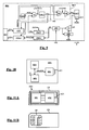
- FIG. 5 shows an oscillator circuit OSC11 comprising an oscillator core of astable multivibrator type (also called astable oscillator).
- This oscillator core comprises two self-inductances L1, L2, a capacitor C1, two transistors T1, T2 of the MOS type and a current source CG1.
- the inductor L1 is connected between a supply node receiving a voltage Vcc and a node N1.
- the inductor L2 is connected between the voltage supply node Vcc and a node N2.
- the capacitor C1 is connected between the nodes N1, N2.
- the transistor T1 has its source S connected to the node N1, its drain D connected to ground via the current source CG1, and its gate G connected to the node N2.
- the transistor T2 has its source S connected to the node N2, its drain D connected to ground via the current source CG1 and its gate G connected to the node N1.
- the synchronization input of the oscillator circuit OSC11 is formed by the base B of a transistor bipolar T3 whose emitter E is connected to ground and whose collector C is connected to the node N1.
- the output of the oscillator circuit is formed by an inverting gate I1 providing the signal CKs, whose input and connected to the node N1, on which the internal oscillation signal CKi is present.
- the phase of the signal CKi on the node N1 is imposed by the signal CKe.
- the heart of the oscillator circuit does not work as an astable oscillator but as a monostable oscillator.
- the transistor T3 When the signal MSK is equal to 0, the transistor T3 is no longer conductive and the heart of the oscillator circuit operates in astable oscillator mode and oscillates freely at a self-oscillation frequency.
- This frequency is set as close as possible to the frequency of the signal CKe (13.56 MHz in the context of the aforementioned standards) by a suitable choice of inductors L1, L2 and capacitor C1.
- the oscillator circuit OSC1 may be of the digital type and configured to, in the synchronous oscillation mode, analyze and memorize the frequency of the signal CKe received on the synchronization input, and copy the signal CKe on its exit. When it switches to the free oscillation mode, the oscillator circuit reconstructs the signal CKs from this stored value.
- the figure 6 shows an oscillator circuit OSC12 comprising a phase locked loop ("Phase Locked Loop").
- the OSC12 circuit comprises an exclusive OR gate G10, an active low pass filter FT1, a VCO (voltage controlled oscillator), a follower circuit SCT and a gate G11 of the type ET.
- the VCO provides the internal oscillation signal CKi. This is applied to the SCT circuit whose output provides the signal internal clock CKs.
- the internal oscillation signal CKi is also returned to an input of the gate G10 via the gate G11, which receives on another input the signal MSK.
- Another input of the gate G10 forms the synchronization input of the circuit OSC12 and is connected to the output of the gate G1, which supplies the external clock signal CKe when the signal MSK is equal to 1.
- the gate G10 forms a phase comparator and its output is sent to a control input of the VCO via the active low-pass filter FT1.
- the gate G11 When the signal MSK is equal to 1, the gate G11 is conducting, the gate G10 receives both the signal CKi and the signal CKe and provides a phase difference signal. This differential signal forms, after low-pass filtering, a reference voltage of the VCO. The signal CKi is thus slaved in phase with the signal CKe. When the signal MSK goes to 0, the outputs of the gates G1 and G11 go to 0. The output of the gate G10 is forced to 0.
- Means are used to maintain at the entrance of the VCO the set voltage that it received before the transition to 0 of the signal MSK. These means comprise for example a voltage source arranged in the active low-pass filter FT1, such as a charge pump. Thus, the VCO continues to provide the signal CKi and maintains the phase of the signal CKi close to that of the signal CKe.
- FIGS. 7A to 7E schematically illustrate a DTr data receiving sequence (left side of the figures) and a DTx data transmission sequence (right side of the figures).
- the Figure 7A shows the shape of the AS antenna signal.
- the Figure 7B represents the modulation signal MS (DTr) extracted from the antenna signal AS by the DMCT circuit.
- the Figure 7C represents the active charge modulation signal Sm1 comprising bursts of the signal CKs.
- the Figure 7D represent the modulation signal MS (DTx) and the figure 7E represents the signal CKs.
- the signal AS here is a full alternating alternating signal which is the image of the magnetic field FLD1 in reception mode.
- Embodiments of the antenna circuit ACT may however comprise a rectifying diode of the antenna signal. In this case, this one is a half-wave signal.
- the external device EDV (Cf. Fig. 1 modulates the amplitude of the magnetic field FLD1 with a modulation depth which depends on the chosen communication protocol, and the antenna signal AS has a similar amplitude modulation.
- NM non-modulation periods are distinguished where the amplitude of the antenna signal is maximum and modulation periods AM where the amplitude of the antenna signal is minimal.
- the maximum and minimum voltage of the signal AS depend in practice on the distance between the external device EDV and the device ND1.
- the antenna signal AS also has non-modulation periods NM where its amplitude is identical to that observed during the non-modulation periods when receiving data.
- the amplitude of the antenna signal then depends only on the magnetic field FLD1 emitted by the external device EDV and the distance between the two devices.
- the AS signal also has ALM boost periods when sending FLD2 magnetic field bursts. Indeed, the signal CKs is then injected into the antenna circuit and is superimposed on the signal induced by the external magnetic field FLD1.
- the antenna signal then comprises an induced component and an injected component.
- the modulation circuit MCT may comprise, in addition to the active charge modulation means that have just been described, conventional passive charge modulation means, such as a load modulation switch connected to the antenna circuit ACT.
- the signal MSK is applied to the gain control circuit AGC and the latter is configured to force the output of the amplifier A2 to 0. In this case, it may not be necessary to prevent the application of the signal CKe on the synchronization input of the oscillator circuit OSC1, which automatically switches to the free oscillation mode when the signal CKe goes to 0.
- the device ND1 may also comprise means for extracting a supply voltage Vcc from the antenna signal, such as a rectifier circuit followed by a smoothing capacitor, to enable the device ND1 to operate in the operating mode. purely passive in the absence of a local power supply.
- the device ND1 also comprises an oscillator OSC2 which is not synchronized with the external clock signal CKe, for example a quartz oscillator.
- the oscillator OSC2 provides a clock signal CK2 enabling the device DV1 to operate in NFC reader mode to communicate with a passive contactless integrated circuit or with a similar device configured in passive mode.
- the synchronous oscillator circuit OSC1 may continue to be used to provide the internal clock signal CKs.
- the selection of the clock signal CKe or CK2 applied to the synchronization input of the circuit OSC1 can be made by means of the DET signal described above, giving priority to the passive mode.
- Gate G3 is an AND gate having three inputs including an inverting input.
- Door G4 is an OR gate with two inputs.
- the gate G3 receives on its two non-inverting inputs the signal CK2 and the signal MSK, and receives the signal DET on its inverting input.
- the gate G1 receives on its inputs the signals CK2, DET and CKe.
- the outputs of the gates G1 and G3 are applied to the gate G4 whose output is connected to the synchronization input of the oscillator circuit OSC1.
- the output of the gate G3 is forced to 0 and the device operates in passive mode as described above.
- the output of the gate G1 is forced to 0 and the signal MSK is forced to 1 by the circuit MG.
- the clock signal CK2 is applied to the input of the oscillator circuit OSC1, for the permanent emission of the magnetic field FLD1.
- the structure of the gate G2, receiving the signals CKs and MS (DTx) and supplying the signal Sm1 can be modified so that it provides a modulation of the signal CKs with an adjustable modulation depth of less than 100%, especially if the device must comply with ISO 14443A and 1443B.
- the device ND1 comprises a phase shifter DPH.
- This phase shifter is for example arranged at the output of the amplifier A1.
- the phase shifter DPH applies to the antenna signal AS a phase shift Dp and supplies the clock circuit CKCT and the DMCT demodulator circuit with a phase-shifted antenna signal AS '.
- the phase shift Dp can be fixed and determined during the design of the DPH phase shifter.
- the phase shift Dp can be determined dynamically by a PHC command applied to the phase shifter, which specifies the value of the phase shift Dp, for example between 0 and 360 °.
- the phase shifter DPH allows the device ND1 to emit FLD2 magnetic field bursts that have the phase shift Dp relative to the external magnetic field FLD1. This allows for example, in some applications where the communication distance must not exceed a certain threshold (for example for security reasons), to reduce the communication distance below this threshold.
- This embodiment shows that the control of the phase of the signal CKs by means of the synchronous oscillator SO does not only make it possible to aim at a zero phase shift between the magnetic field FLD2 and the magnetic field FLD1. Controlling the phase of the signal CKs by means of the synchronous oscillator SO may also make it possible to control a deliberate desynchronization of the magnetic field FLD2 relative to the magnetic field FLD1, while keeping the phase shift Dp between the two as constant as possible. magnetic fields.
- the data transmission / reception device ND1 is also capable of various applications.
- the device ND1 is integrated in a portable device HD1 and is connected to one or more host processors, here two host processors HP1, HP2 which use the device ND1 as contactless communication interface (NFC interface).
- the portable device HD1 is for example a mobile phone, a digital audio player, a digital personal assistant (PDA).
- the processor HP1 may be the main processor of the device, or a secure processor such as a SIM card processor.
- the HP2 processor can for example being the baseband processor of a mobile phone, also providing GSM channel communications.
- the device ND1 is connected to a host processor HP1 and the assembly is integrated in a plastic support CD to form a smart card HD2.
- the antenna coil AC1 is for example a coplanar coil having one or more turns.
- the HD2 card is equipped with a CP group of contacts.
- the HD2 card can for example form an NFC SIM card.
- the group of contacts can in this case include contacts C1 to C8 according to ISO 7816.
- the HD2 card can also form a SD type card to be inserted into any device (mobile phone, personal computer, ...) as an NFC communication interface.
Landscapes
- Engineering & Computer Science (AREA)
- Computer Networks & Wireless Communication (AREA)
- Signal Processing (AREA)
- Computer Hardware Design (AREA)
- Microelectronics & Electronic Packaging (AREA)
- Physics & Mathematics (AREA)
- General Physics & Mathematics (AREA)
- Theoretical Computer Science (AREA)
- Near-Field Transmission Systems (AREA)
- Amplitude Modulation (AREA)
Claims (16)
- Verfahren zum Senden von Daten durch induktive Kopplung, umfassend die folgenden Schritte:- Empfang eines Antennensignals (AS, AS') mittels eines induktiven Antennenkreises (ACT, AC1) in Gegenwart eines externen magnetischen Wechselfelds (FLD1),- Extraktion eines ersten periodischen Signals (CKe) aus dem Antennensignal (AS, AS'),- Generierung eines zweiten periodischen Signals (CKs) mittels eines Synchronoszillators (SO, OSC1), der einen, das erste periodische Signal (CKe) empfangenden Synchronisierungseingang aufweist, wobei der Oszillator einen auf das erste periodische Signal phasenabgeglichenen Synchron-Oszillationsmodus und einen freien Oszillationsmodus aufweist, und- Anlegen von Bursts des zweiten periodischen Signals (CKs) an den Antennenkreis, um ein Magnetfeld (FLD2) zur aktiven Lastmodulation zu generieren,
dadurch gekennzeichnet, dass es die folgenden Schritte umfasst:- Schalten des Oszillators in den Synchron-Oszillationsmodus vor jedem Anlegen eines Bursts des zweiten periodischen Signals (CKs) an den Antennenkreis, und- Schalten des Oszillators in einen freien Oszillationsmodus während dem Anlegen eines Bursts des zweiten periodischen Signals (CKs) an den Antennenkreis. - Verfahren nach Anspruch 1, umfassend den Schritt, der darin besteht, den Oszillator nach dem Anlegen eines Bursts des zweiten periodischen Signals (CKs) an den Antennenkreis während einer Stabilisierungsdauer des Antennensignals im freien Oszillationsmodus zu halten, bevor er wieder in den Synchron-Oszillationsmodus geschaltet wird.
- Verfahren nach einem der Ansprüche 1 und 2, umfassend die folgenden Schritte:- Abgabe eines Daten tragenden Modulationssignals (MS(DTx)),- Anlegen des zweiten periodischen Signals (CKs) an den Antennenkreis, wenn das Modulationssignal (MS(DTx)) einen ersten logischen Wert aufweist,- Generierung eines Maskierungssignals mit einem Maskierungswert wenigstens dann, wenn das Modulationssignal (MS(DTx)) den ersten logischen Wert aufweist, und- Blockierung des Anlegens des ersten periodischen Signals (CKe) am Synchronisierungseingang des Oszillators (SO, OSC1), wenn das Maskierungssignal den Maskierungswert aufweist.
- Verfahren nach den Ansprüchen 2 und 3, umfassend den Schritt, der darin besteht, dem Maskierungswert des Maskierungssignals eine Dauer zu verleihen, die länger ist als die Dauer des ersten logischen Werts des Modulationssignals (MS(DTx)), um den Oszillator während der Stabilisierungsdauer des Antennensignals im freien Oszillationsmodus zu halten.
- Verfahren nach einem der Ansprüche 1 bis 4, umfassend einen Schritt, der darin besteht, das zweite periodische Signal (CKs) in Bezug auf das Antennensignal (AS) zu dephasieren.
- Vorrichtung (ND1) zum Senden und Empfangen von Daten durch induktive Kopplung, umfassend:- einen induktiven Antennenkreis (ACT), in dem ein Antennensignal (AS, AS') in Gegenwart eines externen magnetischen Wechselfelds erscheint,- Mittel (CKCT) zur Extraktion eines ersten periodischen Signals (CKe) aus dem Antennensignal (AS, AS'),- einen Synchronoszillator (SO, OSC1), der einen, das erste periodische Signal (CKe) empfangenden und ein zweites periodisches Signal (CKs) abgebenden Synchronisierungseingang aufweist, wobei der Oszillator einen auf das erste periodische Signal phasenabgeglichenen Synchron-Oszillationsmodus und einen freien Oszillationsmodus aufweist, und- einen Modulationskreis zur aktiven Lastmodulation (MCT), der konfiguriert ist, um an den Antennenkreis Bursts des zweiten periodischen Signals (CKs) anzulegen und ein Magnetfeld (FLD2) zur aktiven Lastmodulation zu generieren,Vorrichtung dadurch gekennzeichnet, dass sie konfiguriert ist, um:- den Oszillator vor jedem Anlegen eines Bursts des zweiten periodischen Signals (CKs) an den Antennenkreis in den Synchron-Oszillationsmodus zu schalten und- den Oszillator während dem Anlegen eines Bursts des zweiten periodischen Signals (CKs) an den Antennenkreis in den freien Oszillationsmodus zu schalten.
- Vorrichtung nach Anspruch 6, die konfiguriert ist, um den Oszillator nach dem Anlegen eines Bursts des zweiten periodischen Signals (CKs) an den Antennenkreis während einer Stabilisierungsdauer des Antennensignals im freien Oszillationsmodus zu halten, bevor er wieder in den Synchron-Oszillationsmodus geschaltet wird.
- Vorrichtung nach einem der Ansprüche 6 und 7, die konfiguriert ist, um:- ein Daten tragendes Lastmodulationssignal (MS(DTx)) zu generieren oder zu empfangen,- das zweite periodische Signal (CKs) an den Antennenkreis anzulegen, wenn das Modulationssignal (MS(DTx)) einen ersten logischen Wert aufweist,- ein Maskierungssignal mit einem Maskierungswert wenigstens dann zu generieren, wenn das Modulationssignal den ersten logischen Wert aufweist, und- das Anlegen des ersten periodischen Signals (CKe) an den Synchronisierungseingang des Oszillators (SO, OSC1) zu blockieren, wenn das Maskierungssignal den Maskierungswert aufweist.
- Vorrichtung nach den Ansprüchen 7 und 8, die konfiguriert ist, um dem Markierungswert des Maskierungssignals (MSK) eine Dauer zu verleihen, die länger ist als die Dauer des ersten logischen Werts des Modulationssignals (MS(DTx)), um den Oszillator während der Stabilisierungsdauer des Antennensignals im freien Oszillationsmodus zu halten.
- Vorrichtung nach einem der Ansprüche 6 bis 9, wobei der Synchronoszillator (SO, OSC1, OSC11) dem Typ der astabilen Oszillatoren gehört, die eine durch Komponenten (L1, L2, C1) des Oszillators festgelegte Eigenfrequenz der Eigenschwingung aufweisen.
- Vorrichtung nach einem der Ansprüche 6 bis 9, wobei der Synchronoszillator (SO, OSC1) dem Typ der digitalen Oszillatoren gehört und konfiguriert ist, um im synchronen Oszillationsmodus die Periode des an den Synchronisierungseingang angelegten periodischen Signals (CKe) am Ausgang zurückzukopieren und im freien Oszillationsmodus die am Synchronisierungseingang im Synchron-Oszillationsmodus erhaltene Frequenz am Ausgang zu rekonstituieren.
- Vorrichtung nach einem der Ansprüche 6 bis 9, wobei der Synchronoszillator (SO, OSC1, OSC12) eine Phasenverriegelungsschleife umfasst, die folgendes beinhaltet:- einen Phasenkomparator (G10), der ein Phasensignal abgibt,- einen aktiven Tiefpaßfilter (FT1), der das Phasensignal empfängt und eine Kontrollspannung abgibt,- einen spannungskontrollierten Oszillator (VCO), der die Kontrollspannung empfängt und das zweite periodische Signal (CKi, CKs) abgibt, und- Mittel (FT1), um den Phasenkomparator (G10) beim Übergang in den freien Oszillationsmodus zu blockieren und den Wert der Kontrollspannung am Eingang des spannungskontrollierten Oszillators (VCO) zu halten.
- Vorrichtung nach einem der Ansprüche 6 bis 12, umfassend Mittel (DPH), um das zweite periodische Signal (CKs) in Bezug auf das Antennensignal (AS) zu dephasieren.
- Vorrichtung (HD1, HD2) umfassend:- eine Datensende- und -empfangsvorrichtung (ND1) nach einem der Ansprüche 6 bis 13, und- wenigstens einen Hostprozessor (HP1, HP2), der zu sendende Daten (Dtx) an die Vorrichtung abgibt.
- Vorrichtung nach Anspruch 14, die in oder auf einem tragbaren Träger (CD) montiert ist.
- Chipkarte (HD2) umfassend wenigstens einen Prozessor (HP1, HP2) und eine Datensende- und -empfangsvorrichtung (ND1) nach einem der Ansprüche 6 bis 13.
Applications Claiming Priority (1)
| Application Number | Priority Date | Filing Date | Title |
|---|---|---|---|
| FR1003754A FR2965082B1 (fr) | 2010-09-21 | 2010-09-21 | Procede et dispositif de modulation de charge active par couplage inductif |
Publications (2)
| Publication Number | Publication Date |
|---|---|
| EP2431925A1 EP2431925A1 (de) | 2012-03-21 |
| EP2431925B1 true EP2431925B1 (de) | 2013-04-17 |
Family
ID=44211855
Family Applications (2)
| Application Number | Title | Priority Date | Filing Date |
|---|---|---|---|
| EP11181125.3A Active EP2431925B1 (de) | 2010-09-21 | 2011-09-13 | Verfahren und Vorrichtung für aktive Lastmodulation durch induktive Kopplung |
| EP11771252.1A Active EP2625653B1 (de) | 2010-09-21 | 2011-09-21 | Verfahren und vorrichtung zur modulation einer aktiven ladung mit der dämpfung von eigenschwingung |
Family Applications After (1)
| Application Number | Title | Priority Date | Filing Date |
|---|---|---|---|
| EP11771252.1A Active EP2625653B1 (de) | 2010-09-21 | 2011-09-21 | Verfahren und vorrichtung zur modulation einer aktiven ladung mit der dämpfung von eigenschwingung |
Country Status (8)
| Country | Link |
|---|---|
| US (5) | US8838023B2 (de) |
| EP (2) | EP2431925B1 (de) |
| KR (1) | KR101819072B1 (de) |
| CN (1) | CN102411698B (de) |
| CA (1) | CA2752757C (de) |
| ES (2) | ES2421618T3 (de) |
| FR (1) | FR2965082B1 (de) |
| WO (1) | WO2012038664A2 (de) |
Cited By (2)
| Publication number | Priority date | Publication date | Assignee | Title |
|---|---|---|---|---|
| US10560255B2 (en) | 2017-07-12 | 2020-02-11 | Stmicroelectronics Sa | Method for synchronizing an active load modulation clock within a transponder, and corresponding transponder |
| US11126906B2 (en) | 2019-06-11 | 2021-09-21 | Nxp B.V. | Transponder and corresponding operating method |
Families Citing this family (67)
| Publication number | Priority date | Publication date | Assignee | Title |
|---|---|---|---|---|
| US7581678B2 (en) | 2005-02-22 | 2009-09-01 | Tyfone, Inc. | Electronic transaction card |
| US12147863B2 (en) | 2008-08-08 | 2024-11-19 | Icashe, Inc. | Method and apparatus for transmitting data via NFC for mobile applications including mobile payments and ticketing |
| US8451122B2 (en) | 2008-08-08 | 2013-05-28 | Tyfone, Inc. | Smartcard performance enhancement circuits and systems |
| FR2965082B1 (fr) | 2010-09-21 | 2012-09-28 | Inside Contactless | Procede et dispositif de modulation de charge active par couplage inductif |
| FR2974209B1 (fr) * | 2011-04-14 | 2013-06-07 | Commissariat Energie Atomique | Procede de detection d'un recepteur sans contact |
| SI23786A (sl) | 2011-06-29 | 2012-12-31 | Ids D.O.O. | Postopek in vezje za visokofrekvenčno komuniciranje med izpraševalnikom in pametno nalepko |
| US9331378B2 (en) * | 2012-05-29 | 2016-05-03 | Nxp B.V. | Active load modulation antenna |
| US8934836B2 (en) | 2012-06-28 | 2015-01-13 | Broadcom Corporation | NFC device with PLL controlled active load modulation |
| GB2519027B (en) | 2012-07-17 | 2020-07-08 | Milwaukee Electric Tool Corp | Universal protocol for power tools |
| US20140087657A1 (en) * | 2012-09-27 | 2014-03-27 | Broadcom Corporation | Remote Antenna Driver for Reducing Unwanted Electromagnetic Emissions and/or Distortion Within a Near Field Communication (NFC) Capable Device |
| US9601930B2 (en) * | 2012-09-28 | 2017-03-21 | Broadcom Corporation | Power transmitting device having device discovery and power transfer capabilities |
| SI24283A (sl) * | 2013-01-15 | 2014-07-31 | Ams R&D Analogni Polprevodniki, D.O.O. | Postopek in vezje aktivne pametne nalepke za komuniciranje z izpraševalnikom |
| US9513609B2 (en) | 2013-02-01 | 2016-12-06 | Nxp B.V. | Wireless communications using active modulation |
| KR102072522B1 (ko) | 2013-03-07 | 2020-02-03 | 삼성전자주식회사 | 비접촉 통신 장치 및 그것을 포함한 유저 장치 |
| US9727767B2 (en) | 2013-03-12 | 2017-08-08 | Nxp B.V. | Clock synchronization in an RFID equipped device |
| EP2816737B1 (de) * | 2013-06-19 | 2016-06-01 | ST-Ericsson SA | Sichere Nahfeldkommunikation |
| EP2824612B1 (de) | 2013-07-08 | 2018-04-18 | STMicroelectronics International N.V. | RFID-Transpondervorrichtung und Verfahren zur Herstellung einer RFID-Transpondervorrichtung |
| FR3010817B1 (fr) * | 2013-09-13 | 2016-12-23 | Inside Secure | Procede et dispositif d'emission de donnees par couplage inductif a auto-oscillation controlee |
| US20150091523A1 (en) * | 2013-10-02 | 2015-04-02 | Mediatek Singapore Pte. Ltd. | Wireless charger system that has variable power / adaptive load modulation |
| CN104660536A (zh) * | 2013-11-21 | 2015-05-27 | 北京同方微电子有限公司 | 一种有源标签直接发送副载波的调制系统 |
| EP2988427B1 (de) * | 2014-08-22 | 2019-04-24 | STMicroelectronics International N.V. | Verfahren für eine Phasenkalibrierung in einer Frontendschaltung einer Nahfeldkommunikation, NFC, Etikettierungsvorrichtung, Frontendschaltung einer NFC-Etikettierungsvorrichtung |
| US9577718B2 (en) * | 2014-11-19 | 2017-02-21 | Qualcomm Incorporated | Systems and methods for inductively coupled communications |
| US10211887B2 (en) | 2015-02-10 | 2019-02-19 | Sony Corporation | Receiver and communication system |
| US9673964B2 (en) * | 2015-02-18 | 2017-06-06 | Qualcomm Incorporated | Active load modulation in near field communication |
| EP3273609B1 (de) | 2015-03-17 | 2021-03-03 | Sony Corporation | Kommunikationsvorrichtung und kommunikationsverfahren |
| EP3076552B1 (de) * | 2015-03-30 | 2019-01-30 | Nxp B.V. | Digitaler synchronisator |
| EP3121755B1 (de) * | 2015-07-21 | 2019-03-13 | STMicroelectronics International N.V. | Radiofrequenzidentifikationstransponder und verfahren zur datenübertragung mittels funkfrequenzidentifikationstechnologie |
| EP3145092B1 (de) | 2015-09-21 | 2019-06-19 | STMicroelectronics International N.V. | Verfahren und senderschaltung zur kommunikation mit aktiver belastungsmodulation in rfid-systemen |
| TW201717570A (zh) * | 2015-11-09 | 2017-05-16 | 新力股份有限公司 | 通信裝置及通信方法 |
| US10019608B2 (en) | 2015-12-09 | 2018-07-10 | Nxp B.V. | Method and device for phase calibration with active load modulation |
| EP3232374B1 (de) * | 2016-04-14 | 2019-12-04 | STMicroelectronics International N.V. | Funkfrequenzidentifikationstransponder und verfahren zum senden einer funkfrequenzidentifikationsnachricht |
| US10396975B2 (en) | 2016-06-29 | 2019-08-27 | Maxim Integrated Products, Inc. | Clock recovery system and method for near field communication with active load modulation |
| US9755679B1 (en) | 2016-07-08 | 2017-09-05 | Nxp B.V. | Load dependent receiver configuration |
| FR3054760A1 (fr) * | 2016-07-27 | 2018-02-02 | Stmicroelectronics Sa | Procede de communication sans contact entre un objet, par exemple un telephone mobile emule en mode carte, et un lecteur par modulation active de charge |
| US9935689B2 (en) | 2016-08-01 | 2018-04-03 | Nxp B.V. | Method and system to measure the phase offset based on the frequency response in a NFC system |
| US10756881B2 (en) * | 2016-08-01 | 2020-08-25 | Nxp B.V. | Method and system for operating a communications device that communicates via inductive coupling |
| US9997829B2 (en) * | 2016-08-03 | 2018-06-12 | Nxp B.V. | Modulation control through adaptive phase adjustment |
| US9911075B1 (en) | 2016-09-01 | 2018-03-06 | Nxp B.V. | RFID transponder and method for supplying energy thereto |
| SG10201608437WA (en) * | 2016-10-07 | 2018-05-30 | Huawei Int Pte Ltd | Active load modulation technique in near field communication |
| US10491437B2 (en) | 2017-01-11 | 2019-11-26 | Mediatek Singapore Pte. Ltd. | Circuits for amplitude demodulation and related methods |
| US10447350B2 (en) | 2017-01-11 | 2019-10-15 | Mediatek Singapore Pte. Ltd. | High-speed circuits for active load modulation and related methods |
| US10374848B2 (en) | 2017-01-11 | 2019-08-06 | Mediatek Singapore Pte. Ltd. | Amplitude demodulators and related methods |
| US9883383B1 (en) | 2017-01-27 | 2018-01-30 | Microsoft Technology Licensing, Llc | Secure near field communications |
| EP3399655B1 (de) * | 2017-05-02 | 2020-07-01 | STMicroelectronics razvoj polprevodnikov d.o.o. | Synchronisierungsverfahren einer aktiven belastungsmodulationsuhr in einem transponder und entsprechender transponder |
| US11063637B2 (en) | 2017-05-09 | 2021-07-13 | The Regents Of The University Of California | Systems and methods for low-power near-field-communication |
| CN108933613B (zh) * | 2017-05-23 | 2021-11-19 | 联发科技(新加坡)私人有限公司 | 用于有源负载调制的方法及通信装置 |
| WO2019009938A1 (en) | 2017-07-05 | 2019-01-10 | Milwaukee Electric Tool Corporation | ADAPTERS FOR COMMUNICATION BETWEEN ELECTRIC TOOLS |
| WO2019036519A1 (en) | 2017-08-14 | 2019-02-21 | The Regents Of The University Of California | LOAD-INDUCED RESONANCE DISPLACEMENT MODULATION SCHEME FOR SIMULTANEOUS TRANSMISSION OF NEAR-FIELD WIRELESS ENERGY AND DATA THROUGH A PAIR OF INDUCTIVE COIL |
| US10567092B2 (en) * | 2017-09-01 | 2020-02-18 | Nxp B.V. | System to calibrate phase using system information |
| US10511347B2 (en) * | 2017-11-14 | 2019-12-17 | Nxp B.V. | Device detection in contactless communication systems |
| EP3512107B1 (de) | 2018-01-11 | 2020-07-15 | Nxp B.V. | Modulationssendeempfänger mit aktiver ladung |
| FR3076972A1 (fr) * | 2018-01-15 | 2019-07-19 | Stmicroelectronics (Grenoble 2) Sas | Procede de synchronisation de signaux au sein d'un dispositif sans contact communiquant avec un lecteur par une modulation active de charge, et dispositif correspondant |
| FR3077174B1 (fr) * | 2018-01-19 | 2021-04-09 | St Microelectronics Sa | Synchronisation entre un lecteur et un objet communiquant sans contact avec le lecteur par modulation active de charge |
| FR3080476A1 (fr) * | 2018-04-24 | 2019-10-25 | Stmicroelectronics (Rousset) Sas | Procede de reglage de la phase du signal emis par un objet capable de communiquer sans contact avec un lecteur par modulation active de charge, et objet correspondant |
| US11011053B2 (en) | 2018-07-31 | 2021-05-18 | Tti (Macao Commercial Offshore) Limited | Systems and methods for remote power tool device control |
| DE102018212957B3 (de) | 2018-08-02 | 2020-01-02 | Fraunhofer-Gesellschaft zur Förderung der angewandten Forschung e.V. | Übertragung von daten von einem benutzerendgerät zu einem anderen gerät |
| DE102018214716A1 (de) | 2018-08-30 | 2020-03-05 | Fraunhofer-Gesellschaft zur Förderung der angewandten Forschung e.V. | Übertragung von daten zwischen einem benutzerendgerät und einem anderen gerät |
| US10771116B2 (en) * | 2018-09-12 | 2020-09-08 | The University Of Vermont And State Agricultural College | Vibrating magnet antenna |
| DE102018124480B4 (de) * | 2018-10-04 | 2020-12-10 | Infineon Technologies Ag | Kommunikationsvorrichtung und verfahren zum betreiben eines antennenschwingkreises |
| KR102640294B1 (ko) | 2018-11-27 | 2024-02-22 | 삼성전자주식회사 | Nfc 회로 및 이의 동작 방법 |
| DE102019201152B3 (de) | 2019-01-30 | 2020-06-18 | Fraunhofer-Gesellschaft zur Förderung der angewandten Forschung e.V. | Bidirektionale Konfiguration von Sensorknoten mit Mobiltelefon ohne Erweiterung |
| EP3703269B1 (de) | 2019-02-26 | 2022-06-08 | Nxp B.V. | Phasenabgleich eines steuergerätetakts mit einem feld |
| DE102019206836A1 (de) | 2019-05-10 | 2020-11-12 | Fraunhofer-Gesellschaft zur Förderung der angewandten Forschung e.V. | Effiziente Kommunikation zur Konfiguration von Sensorknoten |
| US12154111B2 (en) | 2020-09-09 | 2024-11-26 | Icashe, Inc. | Digital document validation |
| US12273937B2 (en) | 2021-02-16 | 2025-04-08 | Milwaukee Electric Tool Corporation | Communication between a wireless dust extractor and a power tool |
| US11848668B2 (en) * | 2022-03-11 | 2023-12-19 | Microchip Technology Incorporated | Apparatus and method for active inductor modulation |
| FR3133508B1 (fr) | 2022-03-11 | 2024-03-15 | St Microelectronics Grenoble 2 | Dispositif comportant un circuit de synchronisation pour realiser une communication en champ proche |
Family Cites Families (33)
| Publication number | Priority date | Publication date | Assignee | Title |
|---|---|---|---|---|
| US3701150A (en) | 1970-06-11 | 1972-10-24 | Motorola Inc | Rf transmission and detection system |
| CA1229926A (en) * | 1984-07-30 | 1987-12-01 | Larry J. Conway | Intelligent broad band digital rf memory |
| US4916329A (en) * | 1987-10-05 | 1990-04-10 | Square D Company | Uninterruptible power supply |
| US5251235A (en) * | 1988-06-14 | 1993-10-05 | Bengt Henoch | Single receiver for receiving wireless transmission of signals is for use with a serial two-conductor data bus |
| US5453667A (en) * | 1992-06-30 | 1995-09-26 | Toshiba Lighting & Technology Corporation | Inverter having frequency changing function |
| US5450088A (en) | 1992-11-25 | 1995-09-12 | Texas Instruments Deutschland Gmbh | Transponder arrangement |
| US5453748A (en) * | 1993-11-15 | 1995-09-26 | Westinghouse Norden Systems | Method and apparatus for responding to an interrogation signal |
| JPH09218263A (ja) | 1995-10-11 | 1997-08-19 | Texas Instr Inc <Ti> | トランスポンダ・システム及びその動作方法 |
| US5929779A (en) | 1996-05-31 | 1999-07-27 | Lucent Technologies Inc. | Read/write protocol for radio frequency identification tags |
| CN1214674C (zh) | 1997-06-16 | 2005-08-10 | 瑞士电信流动电话公司 | 外部装置和芯片卡之间用于通信的芯片卡和方法 |
| BR0108929A (pt) * | 2000-03-01 | 2003-06-03 | Geir Monsen Vavik | Transponder para amplificação de um sinal recebido dentro de um elemento de recepção uso de pelo menos um transponder, sistema de transponder para redes sem fio e com fio, e, uso do mesmo |
| FR2815490B1 (fr) * | 2000-10-16 | 2006-07-07 | Inside Technologies | Lecteur de circuit integre sans contact |
| US6314002B1 (en) | 2000-11-20 | 2001-11-06 | Philips Electronics North America Corporation | Voltage clamping system and method for a DC/DC power converter |
| US7106246B1 (en) * | 2003-02-05 | 2006-09-12 | Kevin W Lindell | Oscillator coupled to an antenna and an application |
| GB2406023B (en) | 2003-10-29 | 2005-08-10 | Innovision Res & Tech Plc | RFID apparatus |
| DE102005005436A1 (de) * | 2004-04-14 | 2005-11-24 | Atmel Germany Gmbh | Sicherheitseinrichtung für einen Transponder |
| DE102004031092A1 (de) | 2004-06-28 | 2006-01-12 | Giesecke & Devrient Gmbh | Transpondereinheit |
| JP4738771B2 (ja) * | 2004-07-29 | 2011-08-03 | ルネサスエレクトロニクス株式会社 | 通信システム、及び通信方法 |
| EP1779680A4 (de) * | 2004-07-30 | 2008-09-17 | Reva Systems Corpoartion | Rfid-etiketten-datenakquisitionssystem |
| US7345539B2 (en) | 2005-02-10 | 2008-03-18 | Raytheon Company | Broadband microwave amplifier |
| JP2007041666A (ja) | 2005-08-01 | 2007-02-15 | Ricoh Co Ltd | Rfidタグ及びその製造方法 |
| DE102005061660A1 (de) * | 2005-12-22 | 2007-06-28 | Giesecke & Devrient Gmbh | Tragbarer Datenträger mit aktiver Kontaktlosschnittstelle |
| EP1895450B1 (de) * | 2006-08-31 | 2014-03-05 | Semiconductor Energy Laboratory Co., Ltd. | Halbleitervorrichtung und Leistungsempfangsvorrichtung |
| DE102007004814B4 (de) * | 2007-01-31 | 2013-06-06 | Continental Automotive Gmbh | Güteanpassung eines Empfangsschaltkreises |
| US8193916B2 (en) | 2007-05-18 | 2012-06-05 | Cambridge Resonant Technologies Ltd. | RFID transmitter |
| DE102007061361A1 (de) | 2007-06-28 | 2009-01-02 | Tamarack Products, Inc., Wauconda | Verfahren zur Herstellung eines RFID-Gegenstandes |
| US9311766B2 (en) | 2007-09-12 | 2016-04-12 | Devicefidelity, Inc. | Wireless communicating radio frequency signals |
| US20090284377A1 (en) | 2008-05-15 | 2009-11-19 | Keystone Technology Solutions, Llc | Flexible RFID Label |
| US7948421B2 (en) * | 2008-06-03 | 2011-05-24 | University Of Louisville Research Foundation, Inc. | Frequency counter based analog-to-digital converter |
| EP2211295A3 (de) | 2009-01-23 | 2011-01-19 | Phytrex Technology Corporation | Auf eine SIM-Karte anwendbare Signalverarbeitungsvorrichtung |
| JP5323517B2 (ja) * | 2009-01-30 | 2013-10-23 | ルネサスエレクトロニクス株式会社 | 半導体装置、携帯通信端末及びマイクロコンピュータ |
| FR2965082B1 (fr) | 2010-09-21 | 2012-09-28 | Inside Contactless | Procede et dispositif de modulation de charge active par couplage inductif |
| DE102011101763A1 (de) | 2011-05-17 | 2012-11-22 | Giesecke & Devrient Gmbh | Phasenkopplung der Signale eines Datenträgers und eines Lesegeräts |
-
2010
- 2010-09-21 FR FR1003754A patent/FR2965082B1/fr not_active Expired - Fee Related
-
2011
- 2011-09-13 EP EP11181125.3A patent/EP2431925B1/de active Active
- 2011-09-13 ES ES11181125T patent/ES2421618T3/es active Active
- 2011-09-13 CA CA2752757A patent/CA2752757C/fr not_active Expired - Fee Related
- 2011-09-19 US US13/235,701 patent/US8838023B2/en active Active
- 2011-09-21 US US13/976,527 patent/US9331748B2/en active Active
- 2011-09-21 EP EP11771252.1A patent/EP2625653B1/de active Active
- 2011-09-21 WO PCT/FR2011/052183 patent/WO2012038664A2/fr not_active Ceased
- 2011-09-21 KR KR1020110095238A patent/KR101819072B1/ko active Active
- 2011-09-21 CN CN201110280874.3A patent/CN102411698B/zh active Active
- 2011-09-21 ES ES11771252T patent/ES2531200T3/es active Active
-
2016
- 2016-05-02 US US15/144,034 patent/US10305546B2/en active Active
-
2017
- 2017-02-15 US US15/433,884 patent/US9941934B2/en active Active
-
2018
- 2018-04-06 US US15/947,384 patent/US10560156B2/en active Active
Cited By (3)
| Publication number | Priority date | Publication date | Assignee | Title |
|---|---|---|---|---|
| US10560255B2 (en) | 2017-07-12 | 2020-02-11 | Stmicroelectronics Sa | Method for synchronizing an active load modulation clock within a transponder, and corresponding transponder |
| US10841074B2 (en) | 2017-07-12 | 2020-11-17 | Stmicroelectronics Sa | Method for synchronizing an active load modulation clock within a transponder, and corresponding transponder |
| US11126906B2 (en) | 2019-06-11 | 2021-09-21 | Nxp B.V. | Transponder and corresponding operating method |
Also Published As
| Publication number | Publication date |
|---|---|
| KR20120030985A (ko) | 2012-03-29 |
| KR101819072B1 (ko) | 2018-01-16 |
| US20130288599A1 (en) | 2013-10-31 |
| US20170180008A1 (en) | 2017-06-22 |
| CA2752757A1 (fr) | 2012-03-21 |
| EP2431925A1 (de) | 2012-03-21 |
| FR2965082B1 (fr) | 2012-09-28 |
| ES2531200T3 (es) | 2015-03-11 |
| US8838023B2 (en) | 2014-09-16 |
| WO2012038664A2 (fr) | 2012-03-29 |
| US10305546B2 (en) | 2019-05-28 |
| EP2625653A2 (de) | 2013-08-14 |
| US10560156B2 (en) | 2020-02-11 |
| EP2625653B1 (de) | 2014-11-26 |
| CN102411698B (zh) | 2016-08-03 |
| US20120071089A1 (en) | 2012-03-22 |
| FR2965082A1 (fr) | 2012-03-23 |
| US9331748B2 (en) | 2016-05-03 |
| US20180227016A1 (en) | 2018-08-09 |
| CN102411698A (zh) | 2012-04-11 |
| US20160308584A1 (en) | 2016-10-20 |
| US9941934B2 (en) | 2018-04-10 |
| WO2012038664A3 (fr) | 2012-07-19 |
| ES2421618T3 (es) | 2013-09-04 |
| CA2752757C (fr) | 2019-05-07 |
Similar Documents
| Publication | Publication Date | Title |
|---|---|---|
| EP2431925B1 (de) | Verfahren und Vorrichtung für aktive Lastmodulation durch induktive Kopplung | |
| EP3244351B1 (de) | Verfahren und vorrichtung zur datenübertragung mittels induktiver kopplung mit gesteuerter selbstoszillation | |
| US10264540B2 (en) | Active load modulation technique in near field communication | |
| EP2801058B1 (de) | Verfahren zur kommunikation zwischen einer nfc karte mit doppelkontakt- und kontaktloser schnittstelle in einem nfc-endgerät und einer nfc-vorrichtung | |
| EP2697745B1 (de) | Verfahren, schaltung und vorrichtung zur kontaktlosen kommunikation mit aktivierter übertragung | |
| EP1898336A1 (de) | Verfahren zur Verbindung eines kontaktlosen integrierten Schaltkreises mit einem NFC-Modul | |
| KR20210064791A (ko) | Nfc 트랜시버를 위한 클럭 복원 회로, nfc 트랜시버, 및 nfc 트랜시버의 제어 방법 | |
| EP3629487B1 (de) | Schnellsynchronisierung zwischen einem objekt und einem lesegerät, die kontaktlos über eine aktive modulation der ladung kommunizieren | |
| FR2943443A1 (fr) | Procede pour etablir une liaison de donnees entre deux processeurs, notamment dans un chipset nfc | |
| EP1869792A2 (de) | Verfahren zur kontaktlosen kommunikation auf der basis asynchroner modulationen und demodulationen | |
| EP1559066B1 (de) | Integrierte rfid-uhf-schaltung | |
| FR3153712A1 (fr) | Dispositif NFC | |
| FR3112914A1 (fr) | Gestion de la commutation d'un dispositif de communication sans contact d'un mode d'émulation de carte à un mode pair à pair. | |
| HK1165892A (en) | Method and device for active load modulation by inductive coupling | |
| HK1165892B (en) | Method and device for active load modulation by inductive coupling | |
| EP4012613B1 (de) | Verfahren zur entriegelung einer nfc-vorrichtung | |
| US20240106497A1 (en) | Near-field communication chip, phase synchronization method, and electronic device | |
| EP2586166B1 (de) | Phasenmodulationsverfahren eines trägersignals von einem sender zu einem kontaktlosen transponder und dessen implementierungseinrichtung | |
| FR3039944A1 (fr) | Dispositif de communication radiofrequence actif |
Legal Events
| Date | Code | Title | Description |
|---|---|---|---|
| PUAI | Public reference made under article 153(3) epc to a published international application that has entered the european phase |
Free format text: ORIGINAL CODE: 0009012 |
|
| AK | Designated contracting states |
Kind code of ref document: A1 Designated state(s): AL AT BE BG CH CY CZ DE DK EE ES FI FR GB GR HR HU IE IS IT LI LT LU LV MC MK MT NL NO PL PT RO RS SE SI SK SM TR |
|
| AX | Request for extension of the european patent |
Extension state: BA ME |
|
| 17P | Request for examination filed |
Effective date: 20120910 |
|
| GRAP | Despatch of communication of intention to grant a patent |
Free format text: ORIGINAL CODE: EPIDOSNIGR1 |
|
| GRAS | Grant fee paid |
Free format text: ORIGINAL CODE: EPIDOSNIGR3 |
|
| GRAA | (expected) grant |
Free format text: ORIGINAL CODE: 0009210 |
|
| AK | Designated contracting states |
Kind code of ref document: B1 Designated state(s): AL AT BE BG CH CY CZ DE DK EE ES FI FR GB GR HR HU IE IS IT LI LT LU LV MC MK MT NL NO PL PT RO RS SE SI SK SM TR |
|
| REG | Reference to a national code |
Ref country code: GB Ref legal event code: FG4D Free format text: NOT ENGLISH |
|
| REG | Reference to a national code |
Ref country code: CH Ref legal event code: EP |
|
| REG | Reference to a national code |
Ref country code: IE Ref legal event code: FG4D Free format text: LANGUAGE OF EP DOCUMENT: FRENCH |
|
| REG | Reference to a national code |
Ref country code: AT Ref legal event code: REF Ref document number: 607703 Country of ref document: AT Kind code of ref document: T Effective date: 20130515 |
|
| REG | Reference to a national code |
Ref country code: DE Ref legal event code: R096 Ref document number: 602011001377 Country of ref document: DE Effective date: 20130613 |
|
| REG | Reference to a national code |
Ref country code: ES Ref legal event code: FG2A Ref document number: 2421618 Country of ref document: ES Kind code of ref document: T3 Effective date: 20130904 |
|
| REG | Reference to a national code |
Ref country code: AT Ref legal event code: MK05 Ref document number: 607703 Country of ref document: AT Kind code of ref document: T Effective date: 20130417 |
|
| REG | Reference to a national code |
Ref country code: LT Ref legal event code: MG4D |
|
| REG | Reference to a national code |
Ref country code: NL Ref legal event code: VDEP Effective date: 20130417 |
|
| PG25 | Lapsed in a contracting state [announced via postgrant information from national office to epo] |
Ref country code: NO Free format text: LAPSE BECAUSE OF FAILURE TO SUBMIT A TRANSLATION OF THE DESCRIPTION OR TO PAY THE FEE WITHIN THE PRESCRIBED TIME-LIMIT Effective date: 20130717 Ref country code: AT Free format text: LAPSE BECAUSE OF FAILURE TO SUBMIT A TRANSLATION OF THE DESCRIPTION OR TO PAY THE FEE WITHIN THE PRESCRIBED TIME-LIMIT Effective date: 20130417 Ref country code: IS Free format text: LAPSE BECAUSE OF FAILURE TO SUBMIT A TRANSLATION OF THE DESCRIPTION OR TO PAY THE FEE WITHIN THE PRESCRIBED TIME-LIMIT Effective date: 20130817 Ref country code: SE Free format text: LAPSE BECAUSE OF FAILURE TO SUBMIT A TRANSLATION OF THE DESCRIPTION OR TO PAY THE FEE WITHIN THE PRESCRIBED TIME-LIMIT Effective date: 20130417 Ref country code: LT Free format text: LAPSE BECAUSE OF FAILURE TO SUBMIT A TRANSLATION OF THE DESCRIPTION OR TO PAY THE FEE WITHIN THE PRESCRIBED TIME-LIMIT Effective date: 20130417 Ref country code: GR Free format text: LAPSE BECAUSE OF FAILURE TO SUBMIT A TRANSLATION OF THE DESCRIPTION OR TO PAY THE FEE WITHIN THE PRESCRIBED TIME-LIMIT Effective date: 20130718 Ref country code: FI Free format text: LAPSE BECAUSE OF FAILURE TO SUBMIT A TRANSLATION OF THE DESCRIPTION OR TO PAY THE FEE WITHIN THE PRESCRIBED TIME-LIMIT Effective date: 20130417 Ref country code: PT Free format text: LAPSE BECAUSE OF FAILURE TO SUBMIT A TRANSLATION OF THE DESCRIPTION OR TO PAY THE FEE WITHIN THE PRESCRIBED TIME-LIMIT Effective date: 20130819 Ref country code: SI Free format text: LAPSE BECAUSE OF FAILURE TO SUBMIT A TRANSLATION OF THE DESCRIPTION OR TO PAY THE FEE WITHIN THE PRESCRIBED TIME-LIMIT Effective date: 20130417 |
|
| RAP2 | Party data changed (patent owner data changed or rights of a patent transferred) |
Owner name: INSIDE SECURE |
|
| PG25 | Lapsed in a contracting state [announced via postgrant information from national office to epo] |
Ref country code: PL Free format text: LAPSE BECAUSE OF FAILURE TO SUBMIT A TRANSLATION OF THE DESCRIPTION OR TO PAY THE FEE WITHIN THE PRESCRIBED TIME-LIMIT Effective date: 20130417 Ref country code: RS Free format text: LAPSE BECAUSE OF FAILURE TO SUBMIT A TRANSLATION OF THE DESCRIPTION OR TO PAY THE FEE WITHIN THE PRESCRIBED TIME-LIMIT Effective date: 20130417 Ref country code: LV Free format text: LAPSE BECAUSE OF FAILURE TO SUBMIT A TRANSLATION OF THE DESCRIPTION OR TO PAY THE FEE WITHIN THE PRESCRIBED TIME-LIMIT Effective date: 20130417 Ref country code: HR Free format text: LAPSE BECAUSE OF FAILURE TO SUBMIT A TRANSLATION OF THE DESCRIPTION OR TO PAY THE FEE WITHIN THE PRESCRIBED TIME-LIMIT Effective date: 20130417 Ref country code: BG Free format text: LAPSE BECAUSE OF FAILURE TO SUBMIT A TRANSLATION OF THE DESCRIPTION OR TO PAY THE FEE WITHIN THE PRESCRIBED TIME-LIMIT Effective date: 20130717 Ref country code: CY Free format text: LAPSE BECAUSE OF FAILURE TO SUBMIT A TRANSLATION OF THE DESCRIPTION OR TO PAY THE FEE WITHIN THE PRESCRIBED TIME-LIMIT Effective date: 20130417 |
|
| REG | Reference to a national code |
Ref country code: FR Ref legal event code: CA Effective date: 20131112 |
|
| REG | Reference to a national code |
Ref country code: DE Ref legal event code: R081 Ref document number: 602011001377 Country of ref document: DE Owner name: INSIDE SECURE, FR Free format text: FORMER OWNER: INSIDE SECURE, AIX-EN-PROVENCE, FR Effective date: 20131111 |
|
| PLBI | Opposition filed |
Free format text: ORIGINAL CODE: 0009260 |
|
| PG25 | Lapsed in a contracting state [announced via postgrant information from national office to epo] |
Ref country code: EE Free format text: LAPSE BECAUSE OF FAILURE TO SUBMIT A TRANSLATION OF THE DESCRIPTION OR TO PAY THE FEE WITHIN THE PRESCRIBED TIME-LIMIT Effective date: 20130417 Ref country code: CZ Free format text: LAPSE BECAUSE OF FAILURE TO SUBMIT A TRANSLATION OF THE DESCRIPTION OR TO PAY THE FEE WITHIN THE PRESCRIBED TIME-LIMIT Effective date: 20130417 Ref country code: DK Free format text: LAPSE BECAUSE OF FAILURE TO SUBMIT A TRANSLATION OF THE DESCRIPTION OR TO PAY THE FEE WITHIN THE PRESCRIBED TIME-LIMIT Effective date: 20130417 Ref country code: SK Free format text: LAPSE BECAUSE OF FAILURE TO SUBMIT A TRANSLATION OF THE DESCRIPTION OR TO PAY THE FEE WITHIN THE PRESCRIBED TIME-LIMIT Effective date: 20130417 |
|
| PLAX | Notice of opposition and request to file observation + time limit sent |
Free format text: ORIGINAL CODE: EPIDOSNOBS2 |
|
| 26 | Opposition filed |
Opponent name: AMS AG Effective date: 20140117 |
|
| PG25 | Lapsed in a contracting state [announced via postgrant information from national office to epo] |
Ref country code: NL Free format text: LAPSE BECAUSE OF FAILURE TO SUBMIT A TRANSLATION OF THE DESCRIPTION OR TO PAY THE FEE WITHIN THE PRESCRIBED TIME-LIMIT Effective date: 20130417 Ref country code: RO Free format text: LAPSE BECAUSE OF FAILURE TO SUBMIT A TRANSLATION OF THE DESCRIPTION OR TO PAY THE FEE WITHIN THE PRESCRIBED TIME-LIMIT Effective date: 20130417 |
|
| BERE | Be: lapsed |
Owner name: INSIDE SECURE Effective date: 20130930 |
|
| REG | Reference to a national code |
Ref country code: DE Ref legal event code: R026 Ref document number: 602011001377 Country of ref document: DE Effective date: 20140117 |
|
| PG25 | Lapsed in a contracting state [announced via postgrant information from national office to epo] |
Ref country code: MC Free format text: LAPSE BECAUSE OF FAILURE TO SUBMIT A TRANSLATION OF THE DESCRIPTION OR TO PAY THE FEE WITHIN THE PRESCRIBED TIME-LIMIT Effective date: 20130417 |
|
| PLAF | Information modified related to communication of a notice of opposition and request to file observations + time limit |
Free format text: ORIGINAL CODE: EPIDOSCOBS2 |
|
| REG | Reference to a national code |
Ref country code: IE Ref legal event code: MM4A |
|
| PLBB | Reply of patent proprietor to notice(s) of opposition received |
Free format text: ORIGINAL CODE: EPIDOSNOBS3 |
|
| PG25 | Lapsed in a contracting state [announced via postgrant information from national office to epo] |
Ref country code: BE Free format text: LAPSE BECAUSE OF NON-PAYMENT OF DUE FEES Effective date: 20130930 Ref country code: IE Free format text: LAPSE BECAUSE OF NON-PAYMENT OF DUE FEES Effective date: 20130913 |
|
| REG | Reference to a national code |
Ref country code: CH Ref legal event code: PL |
|
| PG25 | Lapsed in a contracting state [announced via postgrant information from national office to epo] |
Ref country code: SM Free format text: LAPSE BECAUSE OF FAILURE TO SUBMIT A TRANSLATION OF THE DESCRIPTION OR TO PAY THE FEE WITHIN THE PRESCRIBED TIME-LIMIT Effective date: 20130417 |
|
| PG25 | Lapsed in a contracting state [announced via postgrant information from national office to epo] |
Ref country code: MT Free format text: LAPSE BECAUSE OF FAILURE TO SUBMIT A TRANSLATION OF THE DESCRIPTION OR TO PAY THE FEE WITHIN THE PRESCRIBED TIME-LIMIT Effective date: 20130417 Ref country code: TR Free format text: LAPSE BECAUSE OF FAILURE TO SUBMIT A TRANSLATION OF THE DESCRIPTION OR TO PAY THE FEE WITHIN THE PRESCRIBED TIME-LIMIT Effective date: 20130417 |
|
| PG25 | Lapsed in a contracting state [announced via postgrant information from national office to epo] |
Ref country code: HU Free format text: LAPSE BECAUSE OF FAILURE TO SUBMIT A TRANSLATION OF THE DESCRIPTION OR TO PAY THE FEE WITHIN THE PRESCRIBED TIME-LIMIT; INVALID AB INITIO Effective date: 20110913 Ref country code: LI Free format text: LAPSE BECAUSE OF NON-PAYMENT OF DUE FEES Effective date: 20140930 Ref country code: CH Free format text: LAPSE BECAUSE OF NON-PAYMENT OF DUE FEES Effective date: 20140930 Ref country code: MK Free format text: LAPSE BECAUSE OF FAILURE TO SUBMIT A TRANSLATION OF THE DESCRIPTION OR TO PAY THE FEE WITHIN THE PRESCRIBED TIME-LIMIT Effective date: 20130417 Ref country code: LU Free format text: LAPSE BECAUSE OF NON-PAYMENT OF DUE FEES Effective date: 20130913 |
|
| REG | Reference to a national code |
Ref country code: FR Ref legal event code: PLFP Year of fee payment: 5 |
|
| REG | Reference to a national code |
Ref country code: DE Ref legal event code: R100 Ref document number: 602011001377 Country of ref document: DE |
|
| REG | Reference to a national code |
Ref country code: FR Ref legal event code: CL Name of requester: FRANCE BREVETS, FR Effective date: 20151027 |
|
| PLCK | Communication despatched that opposition was rejected |
Free format text: ORIGINAL CODE: EPIDOSNREJ1 |
|
| PLBN | Opposition rejected |
Free format text: ORIGINAL CODE: 0009273 |
|
| STAA | Information on the status of an ep patent application or granted ep patent |
Free format text: STATUS: OPPOSITION REJECTED |
|
| 27O | Opposition rejected |
Effective date: 20151113 |
|
| REG | Reference to a national code |
Ref country code: FR Ref legal event code: PLFP Year of fee payment: 6 |
|
| REG | Reference to a national code |
Ref country code: GB Ref legal event code: 732E Free format text: REGISTERED BETWEEN 20170615 AND 20170621 |
|
| REG | Reference to a national code |
Ref country code: FR Ref legal event code: PLFP Year of fee payment: 7 |
|
| REG | Reference to a national code |
Ref country code: FR Ref legal event code: PLFP Year of fee payment: 8 |
|
| PG25 | Lapsed in a contracting state [announced via postgrant information from national office to epo] |
Ref country code: AL Free format text: LAPSE BECAUSE OF FAILURE TO SUBMIT A TRANSLATION OF THE DESCRIPTION OR TO PAY THE FEE WITHIN THE PRESCRIBED TIME-LIMIT Effective date: 20130417 |
|
| REG | Reference to a national code |
Ref country code: ES Ref legal event code: PC2A Owner name: VERIMATRIX Effective date: 20191017 |
|
| REG | Reference to a national code |
Ref country code: DE Ref legal event code: R081 Ref document number: 602011001377 Country of ref document: DE Owner name: INFINEON TECHNOLOGIES AG, DE Free format text: FORMER OWNER: INSIDE SECURE, MEYREUIL, FR Ref country code: DE Ref legal event code: R081 Ref document number: 602011001377 Country of ref document: DE Owner name: VERIMATRIX, FR Free format text: FORMER OWNER: INSIDE SECURE, MEYREUIL, FR |
|
| REG | Reference to a national code |
Ref country code: DE Ref legal event code: R081 Ref document number: 602011001377 Country of ref document: DE Owner name: INFINEON TECHNOLOGIES AG, DE Free format text: FORMER OWNER: VERIMATRIX, MEYREUIL, FR |
|
| P01 | Opt-out of the competence of the unified patent court (upc) registered |
Effective date: 20230519 |
|
| REG | Reference to a national code |
Ref country code: GB Ref legal event code: 732E Free format text: REGISTERED BETWEEN 20230602 AND 20230607 |
|
| REG | Reference to a national code |
Ref country code: ES Ref legal event code: PC2A Owner name: INFINEON TECHNOLOGIES AG Effective date: 20240529 |
|
| PGFP | Annual fee paid to national office [announced via postgrant information from national office to epo] |
Ref country code: IT Payment date: 20250923 Year of fee payment: 15 |
|
| PGFP | Annual fee paid to national office [announced via postgrant information from national office to epo] |
Ref country code: GB Payment date: 20250918 Year of fee payment: 15 |
|
| PGFP | Annual fee paid to national office [announced via postgrant information from national office to epo] |
Ref country code: FR Payment date: 20250922 Year of fee payment: 15 |
|
| PGFP | Annual fee paid to national office [announced via postgrant information from national office to epo] |
Ref country code: DE Payment date: 20251121 Year of fee payment: 15 |
|
| PGFP | Annual fee paid to national office [announced via postgrant information from national office to epo] |
Ref country code: ES Payment date: 20251028 Year of fee payment: 15 |