EP2431494A1 - Barrier film for semiconductor wiring, sintered sputtering target, and method of manufacturing sputtering targets - Google Patents
Barrier film for semiconductor wiring, sintered sputtering target, and method of manufacturing sputtering targets Download PDFInfo
- Publication number
- EP2431494A1 EP2431494A1 EP10764370A EP10764370A EP2431494A1 EP 2431494 A1 EP2431494 A1 EP 2431494A1 EP 10764370 A EP10764370 A EP 10764370A EP 10764370 A EP10764370 A EP 10764370A EP 2431494 A1 EP2431494 A1 EP 2431494A1
- Authority
- EP
- European Patent Office
- Prior art keywords
- target
- particles
- barrier film
- sintered compact
- sputtering
- Prior art date
- Legal status (The legal status is an assumption and is not a legal conclusion. Google has not performed a legal analysis and makes no representation as to the accuracy of the status listed.)
- Granted
Links
Images


Classifications
-
- C—CHEMISTRY; METALLURGY
- C23—COATING METALLIC MATERIAL; COATING MATERIAL WITH METALLIC MATERIAL; CHEMICAL SURFACE TREATMENT; DIFFUSION TREATMENT OF METALLIC MATERIAL; COATING BY VACUUM EVAPORATION, BY SPUTTERING, BY ION IMPLANTATION OR BY CHEMICAL VAPOUR DEPOSITION, IN GENERAL; INHIBITING CORROSION OF METALLIC MATERIAL OR INCRUSTATION IN GENERAL
- C23C—COATING METALLIC MATERIAL; COATING MATERIAL WITH METALLIC MATERIAL; SURFACE TREATMENT OF METALLIC MATERIAL BY DIFFUSION INTO THE SURFACE, BY CHEMICAL CONVERSION OR SUBSTITUTION; COATING BY VACUUM EVAPORATION, BY SPUTTERING, BY ION IMPLANTATION OR BY CHEMICAL VAPOUR DEPOSITION, IN GENERAL
- C23C14/00—Coating by vacuum evaporation, by sputtering or by ion implantation of the coating forming material
- C23C14/22—Coating by vacuum evaporation, by sputtering or by ion implantation of the coating forming material characterised by the process of coating
- C23C14/34—Sputtering
- C23C14/3407—Cathode assembly for sputtering apparatus, e.g. Target
- C23C14/3414—Metallurgical or chemical aspects of target preparation, e.g. casting, powder metallurgy
-
- C—CHEMISTRY; METALLURGY
- C23—COATING METALLIC MATERIAL; COATING MATERIAL WITH METALLIC MATERIAL; CHEMICAL SURFACE TREATMENT; DIFFUSION TREATMENT OF METALLIC MATERIAL; COATING BY VACUUM EVAPORATION, BY SPUTTERING, BY ION IMPLANTATION OR BY CHEMICAL VAPOUR DEPOSITION, IN GENERAL; INHIBITING CORROSION OF METALLIC MATERIAL OR INCRUSTATION IN GENERAL
- C23C—COATING METALLIC MATERIAL; COATING MATERIAL WITH METALLIC MATERIAL; SURFACE TREATMENT OF METALLIC MATERIAL BY DIFFUSION INTO THE SURFACE, BY CHEMICAL CONVERSION OR SUBSTITUTION; COATING BY VACUUM EVAPORATION, BY SPUTTERING, BY ION IMPLANTATION OR BY CHEMICAL VAPOUR DEPOSITION, IN GENERAL
- C23C14/00—Coating by vacuum evaporation, by sputtering or by ion implantation of the coating forming material
- C23C14/22—Coating by vacuum evaporation, by sputtering or by ion implantation of the coating forming material characterised by the process of coating
- C23C14/34—Sputtering
-
- C—CHEMISTRY; METALLURGY
- C23—COATING METALLIC MATERIAL; COATING MATERIAL WITH METALLIC MATERIAL; CHEMICAL SURFACE TREATMENT; DIFFUSION TREATMENT OF METALLIC MATERIAL; COATING BY VACUUM EVAPORATION, BY SPUTTERING, BY ION IMPLANTATION OR BY CHEMICAL VAPOUR DEPOSITION, IN GENERAL; INHIBITING CORROSION OF METALLIC MATERIAL OR INCRUSTATION IN GENERAL
- C23C—COATING METALLIC MATERIAL; COATING MATERIAL WITH METALLIC MATERIAL; SURFACE TREATMENT OF METALLIC MATERIAL BY DIFFUSION INTO THE SURFACE, BY CHEMICAL CONVERSION OR SUBSTITUTION; COATING BY VACUUM EVAPORATION, BY SPUTTERING, BY ION IMPLANTATION OR BY CHEMICAL VAPOUR DEPOSITION, IN GENERAL
- C23C14/00—Coating by vacuum evaporation, by sputtering or by ion implantation of the coating forming material
- C23C14/06—Coating by vacuum evaporation, by sputtering or by ion implantation of the coating forming material characterised by the coating material
- C23C14/14—Metallic material, boron or silicon
- C23C14/16—Metallic material, boron or silicon on metallic substrates or on substrates of boron or silicon
- C23C14/165—Metallic material, boron or silicon on metallic substrates or on substrates of boron or silicon by cathodic sputtering
-
- H—ELECTRICITY
- H01—ELECTRIC ELEMENTS
- H01J—ELECTRIC DISCHARGE TUBES OR DISCHARGE LAMPS
- H01J37/00—Discharge tubes with provision for introducing objects or material to be exposed to the discharge, e.g. for the purpose of examination or processing thereof
- H01J37/32—Gas-filled discharge tubes
- H01J37/34—Gas-filled discharge tubes operating with cathodic sputtering
- H01J37/3411—Constructional aspects of the reactor
- H01J37/3414—Targets
-
- H—ELECTRICITY
- H01—ELECTRIC ELEMENTS
- H01J—ELECTRIC DISCHARGE TUBES OR DISCHARGE LAMPS
- H01J37/00—Discharge tubes with provision for introducing objects or material to be exposed to the discharge, e.g. for the purpose of examination or processing thereof
- H01J37/32—Gas-filled discharge tubes
- H01J37/34—Gas-filled discharge tubes operating with cathodic sputtering
- H01J37/3411—Constructional aspects of the reactor
- H01J37/3414—Targets
- H01J37/3426—Material
-
- H—ELECTRICITY
- H10—SEMICONDUCTOR DEVICES; ELECTRIC SOLID-STATE DEVICES NOT OTHERWISE PROVIDED FOR
- H10D—INORGANIC ELECTRIC SEMICONDUCTOR DEVICES
- H10D64/00—Electrodes of devices having potential barriers
- H10D64/01—Manufacture or treatment
- H10D64/011—Manufacture or treatment of electrodes ohmically coupled to a semiconductor
-
- H—ELECTRICITY
- H10—SEMICONDUCTOR DEVICES; ELECTRIC SOLID-STATE DEVICES NOT OTHERWISE PROVIDED FOR
- H10P—GENERIC PROCESSES OR APPARATUS FOR THE MANUFACTURE OR TREATMENT OF DEVICES COVERED BY CLASS H10
- H10P14/00—Formation of materials, e.g. in the shape of layers or pillars
- H10P14/20—Formation of materials, e.g. in the shape of layers or pillars of semiconductor materials
-
- H—ELECTRICITY
- H10—SEMICONDUCTOR DEVICES; ELECTRIC SOLID-STATE DEVICES NOT OTHERWISE PROVIDED FOR
- H10P—GENERIC PROCESSES OR APPARATUS FOR THE MANUFACTURE OR TREATMENT OF DEVICES COVERED BY CLASS H10
- H10P14/00—Formation of materials, e.g. in the shape of layers or pillars
- H10P14/20—Formation of materials, e.g. in the shape of layers or pillars of semiconductor materials
- H10P14/22—Formation of materials, e.g. in the shape of layers or pillars of semiconductor materials using physical deposition, e.g. vacuum deposition or sputtering
-
- H—ELECTRICITY
- H10—SEMICONDUCTOR DEVICES; ELECTRIC SOLID-STATE DEVICES NOT OTHERWISE PROVIDED FOR
- H10P—GENERIC PROCESSES OR APPARATUS FOR THE MANUFACTURE OR TREATMENT OF DEVICES COVERED BY CLASS H10
- H10P14/00—Formation of materials, e.g. in the shape of layers or pillars
- H10P14/40—Formation of materials, e.g. in the shape of layers or pillars of conductive or resistive materials
- H10P14/42—Formation of materials, e.g. in the shape of layers or pillars of conductive or resistive materials using a gas or vapour
- H10P14/44—Physical vapour deposition [PVD]
-
- H—ELECTRICITY
- H10—SEMICONDUCTOR DEVICES; ELECTRIC SOLID-STATE DEVICES NOT OTHERWISE PROVIDED FOR
- H10W—GENERIC PACKAGES, INTERCONNECTIONS, CONNECTORS OR OTHER CONSTRUCTIONAL DETAILS OF DEVICES COVERED BY CLASS H10
- H10W20/00—Interconnections in chips, wafers or substrates
- H10W20/01—Manufacture or treatment
- H10W20/031—Manufacture or treatment of conductive parts of the interconnections
- H10W20/032—Manufacture or treatment of conductive parts of the interconnections of conductive barrier, adhesion or liner layers
- H10W20/033—Manufacture or treatment of conductive parts of the interconnections of conductive barrier, adhesion or liner layers in openings in dielectrics
Definitions
- the present invention relates to a barrier film for a semiconductor wiring, a sintered compact sputtering target, and a method of producing a sputtering target, and, for example, can be used for forming a barrier film that functions as a reaction prevention layer of a semiconductor device.
- a diffusion barrier film is formed in advance and a copper wiring is thereafter formed. Tantalum or tantalum nitride is generally used as the diffusion barrier film of the copper wiring of the semiconductor element.
- this is performed by depositing tantalum or tantalum nitride by sputtering a high purity tantalum target and forming a diffusion barrier film at the concave part of a groove to which the copper wiring is to be formed, subsequently depositing a seed layer made of copper or copper alloy via sputtering, and ultimately embedding copper based on electroplating.
- Patent Document 1 a barrier film of tantalum silicon nitride has been proposed (refer to Patent Document 1).
- a target having tantalum silicide as its main component is prepared in advance, and this is subject to reactive sputtering in a nitrogen atmosphere to perform nitriding in order to form a barrier film of tantalum silicon nitride.
- Patent Document 1 a high melting point metal-boron-based (boric) diffusion barrier has also been proposed (refer to Non-Patent Document 1).
- the wiring width of semiconductor elements is becoming even narrower pursuant to higher densification and a ternary barrier film of Ta-Si-B or the like with high barrier properties and low resistance is also being considered.
- Patent Document 1 Japanese Published Unexamined Patent Application No. H11-200025
- Patent Document 2 Japanese Published Unexamined Patent Application No. S58-144401
- Patent Document 3 Japanese Published Unexamined Patent Application No. H2-163337
- Patent Document 4 Japanese Published Unexamined Patent Application No. 2003-64440
- KaloyerosA E Eisenbraun E, "Ultrathin diffusion barriers/liners for gigascale copper metallization" Annu Rev Mater Sci, Vol. 30, Pages 363 to 385 (2000 )
- an object of this invention is to provide a sputtering target that is particularly effective for use in forming a barrier film in which the target itself has the same composition as the barrier film without depending on the nitriding reaction in the sputtering process, which is capable of effectively preventing the reaction of a semiconductor device, which is free from the generation of particles in the sputtering process, and which yields superior characteristics upon forming the barrier film, and a method of producing such a target.
- the present invention provides:
- the present invention yields a superior effect of being able to obtain a sputtering target in which the target itself has the same composition as the barrier film without depending on the nitriding reaction in the sputtering process, which is capable of effectively preventing the reaction of a semiconductor device, which is free from the generation of particles in the sputtering process, and, for example, which is particularly effective for use in forming a barrier film, as well as a method of producing such a target and the foregoing barrier film.
- the sputtering target for forming the barrier film of the present invention can be produced by mixing W powder having an average particle size of 1 to 5 ⁇ m and Ni powder having an average particle size of 1 to 30 ⁇ m to achieve a compounding ratio of WxNiy (70 ⁇ x ⁇ 90, 10 ⁇ y ⁇ 30, unit: atomic percent), and sintering this based on hot press at a welding pressure of 10 to 50 MPa and temperature of 1300 to 1600°C.
- These sintering conditions are the conditions for obtaining a sintered compact sputtering target having a composition of WxNiy (70 ⁇ x ⁇ 90, 10 ⁇ y ⁇ 30, unit: at%), and comprising a structure configured from a W matrix and Ni particles existing therein and in which W is diffused in the Ni particles.
- this target can be obtained, there is no particular limitation to the production method.
- the W powder and the Ni powder may have an average particle size that is different from the foregoing conditions. Nevertheless, the intended target can be efficiently obtained by using the powders having the foregoing particle size.
- the Ni amount in the W is a trace amount, the plating properties and adhesiveness tend to deteriorate even if the barrier properties based on the W-Ni alloy are favorable.
- this problem can be solved by devising the plating method such as substituting the plating method with an electroless plating method and adopting the ion beam deposition method, sputtering method or the like.
- the Ni amount in W is more preferably 20 to 30 (20 ⁇ y ⁇ 30).
- favorable plating properties can be obtained even with the electroless plating method.
- the most important aspect is whether a material comprises favorable barrier properties or not.
- the barrier film for a semiconductor wiring of the present invention having a composition of WxNiy yields a superior effect of effectively preventing copper from diffusing in the semiconductor element (silicon) or the insulation film, and eliminate factors that impair the semiconductor properties.
- the sintered compact sputtering target comprises several features, and one of these features is that the matrix of the sputtering target is W and Ni particles of 2 to 40 ⁇ m are uniformly dispersed in the W matrix.
- W itself is crystallized in the sintering process
- Ni particles of 2 to 5 ⁇ m exist at a triple point of the W crystals, and Ni of the other excess portions is uniformly dispersed in the W matrix as particles of 20 to 40 ⁇ m.
- Ni particles of 2 to 40 ⁇ m are uniformly dispersed in the W matrix, but when viewed individually, Ni particles of 2 to 5 ⁇ m and Ni particles of 20 to 40 ⁇ m are dispersed in two types of modes.
- the number of Ni particles that exist will change depending on the contained Ni amount, and in particular the number of Ni particles of 20 to 40 ⁇ m will decrease in proportion to the decrease in the additive amount of Ni.
- the Ni particles existing in the W matrix exist as WNi particles.
- Ni existing independently in the W matrix is undesirable since the magnetic properties of Ni will obstruct the generation of plasma in the sputtering process.
- the existing Ni particles will exist as Ni particles and considerably affect the sputtering efficiency. Accordingly, it could be said that the Ni particles existing in the W matrix desirably exist as WNi particles having non-magnetic properties.
- hot press is performed at 1300°C to 1450°C. If the sintering temperature is less than 1300°C, the Ni particles will not diffuse sufficiently in W, and will exist as Ni particles. Diffusion can be sufficiently performed at 1300°C or higher and 1450°C (upper limit temperature) or less. If the hot press temperature exceeds 1450°C, Ni may melt since the melting point of Ni is 1455°C. Nevertheless, it is easier to increase the density and deoxidation tends to progress easier if the temperature is raised up to the vicinity of the melting point. Accordingly, the hot press temperature is preferably 1450°C or less, and set to 1400°C or less in consideration of safety.
- the purity is 4N5 or higher excluding gas components.
- W-Ni is what functions as the barrier film, and other impurities may contaminate the semiconductor film or the insulation film.
- impurities since the inclusion of impurities is likely to deform the target structure, and the foregoing favorable structure cannot be maintained, it is desirable to use a sputtering target with the highest purity as much as possible.
- oxygen is 1000 wtppm or less and carbon is 50 ppm or less.
- oxygen as a gas component is more preferably 500 wtppm or less.
- gas components also cause the generation of particles.
- films with a high content of oxygen and carbon have high film stress and peel easily.
- the peeling of these films will cause a sudden increase in the generation of particles in the sputtering process.
- oxygen and carbon as gas components are likely to form oxides and carbides with the constituent elements.
- the inclusion of foreign matter such as oxides and carbides will deform or partially destroy the favorable target structure of the present invention, and it could be said that the lower the content of such oxides and carbides, the better.
- the foregoing impurities will not cause a vital problem if contained in a normally included amount, and it should be understood that these impurities are not the crucial impediment of the target function.
- the impurities should be reduced as much as possible for the foregoing reasons.
- the reason why the welding pressure is set to 10 to 50 MPa in the sintering process is because the density cannot be improved as a matter of course if it is a low pressure of less than 10 MPa, and layered cracks are generated parallel to the pressed surface if a high pressure exceeding 50 MPa is applied.
- W powder had an average particle size of 5 ⁇ m and Ni powder had an average particle size of 30 ⁇ m, and these were blended to achieve W90Ni10 and mixed in a ball mill.
- the mixed powder was filled in a carbon mold, heated to 1400°C in a vacuum atmosphere and hot pressed at 30 MPa.
- a sintered compact having a relative density of 100% was thereby obtained.
- the obtained sintered compact was subject to grinding and polishing treatment to prepare a target having a diameter of 330 mm and a thickness of 6.35 mm.
- Oxygen in the target was 120 wtppm and carbon was 30 wtppm.
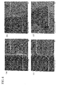
- the SEM image of this target is shown in Fig. 1.
- Fig. 1 (a) is an SEM image of a W-Ni sintered compact surface (polished surface)
- Fig. 1(b) is a mapping image of W based on EDX (energy dispersion X-ray spectrometry) in the same visual field
- Fig. 1(c) is a mapping image of Ni based on EDX in the same visual field.
- the W crystal structure can be observed.
- Fig. 1(b) in the center and rightmost Fig. 1(c) fine Ni particles of 2 to 5 ⁇ m and large Ni particles of 20 to 40 ⁇ m dispersed in the W structure can be observed.
- the sintered compact target processed as described above was bonded with a pure copper backing plate, and the target was set in a radio frequency (RF) sputtering device.
- RF radio frequency
- single crystal Si was set as the substrate to face the target.
- RF sputtering was performed in an argon atmosphere.
- the applied voltage was RF 12 kW and the deposition time was 50 seconds.
- a 15 nm barrier film was thereby formed on the single crystal silicon substrate. The generation status of particles in the foregoing process was observed.
- Example 1 Composition Ratio (at%) Hot Press Temperature (°C) Relative Density (%) Oxygen (wtppm) Carbon (wtppm) Barrier property Plating Property Adhesiveness Sputtering Characteristics
- Example 1 W90Ni10 1400 100 120 30 ⁇ ⁇ ⁇ ⁇ Example 2 W80Ni20 1400 99.9 100 30 ⁇ ⁇ ⁇ ⁇ Example 3 W70Ni30 1400 100 130 20 ⁇ ⁇ ⁇ ⁇ Example 4 W90Ni10 1400 96.1 850 30 ⁇ ⁇ ⁇ ⁇ Example 5 W80Ni20 1400 96.5 730 40 ⁇ ⁇ ⁇ ⁇ Example 6 W70Ni30 1400 97.3 870 30 ⁇ ⁇ ⁇ Comparative Example 1 W80Ni20 1200 87.1 900 20 - - - ⁇ Comparative Example 2 W80Ni20 1000 86.2 840 30 - - - ⁇ Comparative Example 3 W80Ni20 1200 83.4 1340 40 -
- W powder had an average particle size of 5 ⁇ m and Ni powder had an average particle size of 30 ⁇ m, and these were blended to achieve W80Ni20 and mixed in a ball mill.
- the mixed powder was filled in a carbon mold, heated to 1400°C in a vacuum atmosphere and hot pressed at 30 MPa.
- a sintered compact having a relative density of 99.9% was thereby obtained.
- the obtained sintered compact was subject to grinding and polishing treatment to prepare a target having a diameter of 330 mm and a thickness of 6.35 mm.
- Oxygen in the target was 100 wtppm and carbon was 30 wtppm.
- the SEM image of this target is shown in Fig. 2.
- FIG. 2(a) is an SEM image of a W-Ni sintered compact surface (polished surface)
- Fig. 2(b) is a mapping image of W based on EDX (energy dispersion X-ray spectrometry) in the same visual field
- Fig. 2(c) is a mapping image of Ni based on EDX in the same visual field.
- fine Ni particles of 2 to 5 ⁇ m and large Ni particles of 20 to 40 ⁇ m dispersed in the W structure can be observed.
- the number of large Ni particles of 20 to 40 ⁇ m shown in Fig. 2 of Example 2 has increased compared to the number of large Ni particles of 20 to 40 ⁇ m shown in Fig. 1 of Example 1.
- the sintered compact target processed as described above was bonded with a pure copper backing plate, and the target was set in a radio frequency (RF) sputtering device.
- RF radio frequency
- single crystal Si was set as the substrate to face the target.
- RF sputtering was performed in an argon atmosphere.
- the applied voltage was RF 12 kW and the deposition time was 50 seconds.
- a 15 nm barrier film was thereby formed on the single crystal silicon substrate. The generation status of particles in the foregoing process was observed.
- W powder had an average particle size of 5 ⁇ m and Ni powder had an average particle size of 30 ⁇ m, and these were blended to achieve W70Ni30 and mixed in a ball mill.
- the mixed powder was filled in a carbon mold, heated to 1400°C in a vacuum atmosphere and hot pressed at 30 MPa.
- a sintered compact having a relative density of 100% was thereby obtained.
- the obtained sintered compact was subject to grinding and polishing treatment to prepare a target having a diameter of 330 mm and a thickness of 6.35 mm.
- Oxygen in the target was 130 wtppm and carbon was 20 wtppm.
- Fig. 3(a) is an SEM image of a W-Ni sintered compact surface (polished surface)
- Fig. 3(b) is a mapping image of W based on EDX (energy dispersion X-ray spectrometry) in the same visual field
- Fig. 3(c) is a mapping image of Ni based on EDX in the same visual field.
- Fig. 3(b) in the center and Fig. 3(c) on the right, fine Ni particles of 2 to 5 ⁇ m and large Ni particles of 20 to 40 ⁇ m dispersed in the W structure can be observed.
- the number of large Ni particles of 20 to 40 ⁇ m shown in Fig. 3 of Example 3 has increased compared to the number of large Ni particles of 20 to 40 ⁇ m shown in Fig. 2 of Example 2.
- the sintered compact target processed as described above was bonded with a pure copper backing plate, and the target was set in a radio frequency (RF) sputtering device.
- RF radio frequency
- single crystal Si was set as the substrate to face the target.
- RF sputtering was performed in an argon atmosphere.
- the applied voltage was RF 12 kW and the deposition time was 50 seconds.
- a 15 nm barrier film was thereby formed on the single crystal silicon substrate. The generation status of particles in the foregoing process was observed.
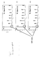
- Fig. 4 shows the obtained line spectrum upon observing the interface of the W-rich particles in (a) the W-10 at% Ni target, (b) the W-20 at% Ni target, and (c) the W-30 at% Ni target, respectively.
- Fig. 4(a) to (c) it was confirmed that Ni is hardly diffused in the W-rich particles and W is diffused in the Ni-rich particles.
- Fig. 4(d) at the lower right part is a result of performing heat treatment at 1400°C for two hours, and it was confirmed that W is diffused in Ni.
- NiW (042) is the main peak of NiW, and the peak intensity is increasing pursuant to the increase in the additive amount of Ni.
- W is diffused in the Ni particles and an intermetallic compound of NiW is formed.
- the peak of Ni could not be confirmed, and it was confirmed that Ni does not exist independently in the target.
- W powder had an average particle size of 1 ⁇ m and Ni powder had an average particle size of 1 ⁇ m, and these were blended to achieve W90Ni10 and mixed in a ball mill.
- the mixed powder was filled in a carbon mold, heated to 1400°C in a vacuum atmosphere and hot pressed at 30 MPa.
- a sintered compact having a relative density of 96.1 % was thereby obtained.
- the obtained sintered compact was subject to grinding and polishing treatment to prepare a target having a diameter of 330 mm and a thickness of 6.35 mm.
- Oxygen in the target was 850 wtppm and carbon was 30 wtppm.
- the amount of oxygen in the target increased compared to Example 1, and the increase in the adsorbed amount of oxygen is considered to be because the used raw material powder was fine.
- the SEM image of this target is omitted, similar to the SEM image shown in Fig. 1 of Example 1, fine Ni particles of 2 to 5 ⁇ m and large Ni particles of 20 to 40 ⁇ m dispersed in the W structure can be observed.
- the sintered compact target processed as described above was bonded with a pure copper backing plate, and the target was set in a radio frequency (RF) sputtering device.
- RF radio frequency
- single crystal Si was set as the substrate to face the target.
- RF sputtering was performed in an argon atmosphere.
- the applied voltage was RF 12 kW and the deposition time was 50 seconds.
- a 15 nm barrier film was thereby formed on the single crystal silicon substrate. The generation status of particles in the foregoing process was observed.
- W powder had an average particle size of 1 ⁇ m and Ni powder had an average particle size of 1 ⁇ m, and these were blended to achieve W80Ni20 and mixed in a ball mill.
- the mixed powder was filled in a carbon mold, heated to 1400°C in a vacuum atmosphere and hot pressed at 30 MPa.
- a sintered compact having a relative density of 96.5% was thereby obtained.
- the obtained sintered compact was subject to grinding and polishing treatment to prepare a target having a diameter of 330 mm and a thickness of 6.35 mm.
- Oxygen in the target was 730 wtppm and carbon was 40 wtppm.
- the amount of oxygen in the target increased compared to Example 2, and the increase in the adsorbed amount of oxygen is considered to be because the used raw material powder was fine.
- the SEM image of this target is omitted, similar to the SEM image shown in Fig. 2 of Example 2, fine Ni particles of 2 to 5 ⁇ m and large Ni particles of 20 to 40 ⁇ m dispersed in the W structure can be observed.
- the sintered compact target processed as described above was bonded with a pure copper backing plate, and the target was set in a radio frequency (RF) sputtering device.
- RF radio frequency
- single crystal Si was set as the substrate to face the target.
- RF sputtering was performed in an argon atmosphere.
- the applied voltage was RF 12 kW and the deposition time was 50 seconds.
- a 15 nm barrier film was thereby formed on the single crystal silicon substrate. The generation status of particles in the foregoing process was observed.
- W powder had an average particle size of 1 ⁇ m and Ni powder had an average particle size of 1 ⁇ m, and these were blended to achieve W70Ni30 and mixed in a ball mill.
- the mixed powder was filled in a carbon mold, heated to 1400°C in a vacuum atmosphere and hot pressed at 30 MPa.
- a sintered compact having a relative density of 97.3% was thereby obtained.
- the obtained sintered compact was subject to grinding and polishing treatment to prepare a target having a diameter of 330 mm and a thickness of 6.35 mm.
- Oxygen in the target was 730 wtppm and carbon was 40 wtppm.
- the amount of oxygen in the target increased compared to Example 3, and the increase in the adsorbed amount of oxygen is considered to be because the used raw material powder was fine.
- the SEM image of this target is omitted, similar to the SEM image shown in Fig. 3 of Example 3, fine Ni particles of 2 to 5 ⁇ m and large Ni particles of 20 to 40 ⁇ m dispersed in the W structure can be observed.
- the sintered compact target processed as described above was bonded with a pure copper backing plate, and the target was set in a radio frequency (RF) sputtering device.
- RF radio frequency
- single crystal Si was set as the substrate to face the target.
- RF sputtering was performed in an argon atmosphere.
- the applied voltage was RF 12 kW and the deposition time was 50 seconds.
- a 15 nm barrier film was thereby formed on the single crystal silicon substrate. The generation status of particles in the foregoing process was observed.
- W powder had an average particle size of 5 ⁇ m and Ni powder had an average particle size of 30 ⁇ m, and these were blended to achieve W80Ni20 and mixed in a ball mill.
- the mixed powder was filled in a carbon mold, heated to 1200°C in a vacuum atmosphere and hot pressed at 30 MPa.
- a sintered compact having a relative density of 87.1 % was thereby obtained.
- the obtained sintered compact was subject to grinding and polishing treatment to prepare a target having a diameter of 330 mm and a thickness of 6.35 mm.
- Oxygen in the target was 900 wtppm and carbon was 20 wtppm.
- the sintered compact target processed as described above was bonded with a pure copper backing plate, and the target was set in a radio frequency (RF) sputtering device.
- RF radio frequency
- single crystal Si was set as the substrate to face the target.
- RF sputtering was performed in an argon atmosphere.
- the applied voltage was RF 12 kW and the deposition time was 50 seconds. Nevertheless, plasma could not be generated and the sputter properties were inferior.
- the reason for this is considered to be that, because the hot press temperature was low, W did not sufficiently diffuse in the Ni particles of the target and existed as pure Ni particles, and plasma was not generated in the sputtering process due to the magnetic properties of the Ni particles.
- W powder had an average particle size of 5 ⁇ m and Ni powder had an average particle size of 30 ⁇ m, and these were blended to achieve W80Ni20 and mixed in a ball mill. Subsequently, the mixed powder was filled in a carbon mold, heated to 1000°C in a vacuum atmosphere and hot pressed at 30 MPa. A sintered compact having a relative density of 86.2% was thereby obtained. Subsequently, the obtained sintered compact was subject to grinding and polishing treatment to prepare a target having a diameter of 330 mm and a thickness of 6.35 mm. Oxygen in the target was 840 wtppm and carbon was 30 wtppm.
- the sintered compact target processed as described above was bonded with a pure copper backing plate, and the target was set in a radio frequency (RF) sputtering device.
- RF radio frequency
- single crystal Si was set as the substrate to face the target.
- RF sputtering was performed in an argon atmosphere.
- the applied voltage was RF 12 kW and the deposition time was 50 seconds.
- plasma could not be generated and the sputter properties were inferior. The reason for this is considered to be that the hot press temperature was low, W did not sufficiently diffuse in the Ni particles of the target and existed as pure Ni particles, and plasma was not generated in the sputtering process due to the magnetic properties of the Ni particles.
- W powder had an average particle size of 1 ⁇ m and Ni powder had an average particle size of 1 ⁇ m, and these were blended to achieve W80Ni20 and mixed in a ball mill.
- the mixed powder was filled in a carbon mold, heated to 1200°C in a vacuum atmosphere and hot pressed at 30 MPa. Since the raw material powder was fine, the amount of oxygen increased much more.
- a sintered compact having a relative density of 83.4% was thereby obtained.
- the obtained sintered compact was subject to grinding and polishing treatment to prepare a target having a diameter of 330 mm and a thickness of 6.35 mm. Oxygen in the target was 1340 wtppm and carbon was 40 wtppm. Since the raw material powder was fine, the amount of oxygen increased much more.
- the sintered compact target processed as described above was bonded with a pure copper backing plate, and the target was set in a radio frequency (RF) sputtering device.
- RF radio frequency
- single crystal Si was set as the substrate to face the target.
- RF sputtering was performed in an argon atmosphere.
- the applied voltage was RF 12 kW and the deposition time was 50 seconds.
- plasma could not be generated and the sputter properties were inferior. The reason for this is considered to be that, because the hot press temperature was low, W did not sufficiently diffuse in the Ni particles of the target and existed as pure Ni particles, and plasma was not generated in the sputtering process due to the magnetic properties of the Ni particles.
- W powder had an average particle size of 1 ⁇ m and Ni powder had an average particle size of 1 ⁇ m, and these were blended to achieve W70Ni30 and mixed in a ball mill. Subsequently, the mixed powder was filled in a carbon mold, heated to 1000°C in a vacuum atmosphere and hot pressed at 30 MPa. A sintered compact having a relative density of 85.8% was thereby obtained. Subsequently, the obtained sintered compact was subject to grinding and polishing treatment to prepare a target having a diameter of 330 mm and a thickness of 6.35 mm. Oxygen in the target was 1200 wtppm and carbon was 30 wtppm. Since the raw material powder was fine, the amount of oxygen increased much more.
- the sintered compact target processed as described above was bonded with a pure copper backing plate, and the target was set in a radio frequency (RF) sputtering device.
- RF radio frequency
- single crystal Si was set as the substrate to face the target.
- RF sputtering was performed in an argon atmosphere.
- the applied voltage was RF 12 kW and the deposition time was 50 seconds.
- plasma could not be generated and the sputter properties were inferior. The reason for this is considered to be that, because the hot press temperature was low, W did not sufficiently diffuse in the Ni particles of the target and existed as pure Ni particles, and plasma was not generated in the sputtering process due to the magnetic properties of the Ni particles.
- the sintered compact sputtering target for forming the barrier film for a semiconductor wiring of the present invention contains Ni with its remainder being W and unavoidable impurities and has the composition of WxNiy (70 ⁇ x ⁇ 90, 10 ⁇ y ⁇ 30), which is essential as barrier film for a semiconductor wiring for a semiconductor.
- WxNiy 70 ⁇ x ⁇ 90, 10 ⁇ y ⁇ 30
- the present invention yields a superior effect of being able to obtain a sputtering target which is effective for use in forming a barrier film without depending on the nitriding reaction in the sputtering process, which is capable of effectively preventing the reaction between layers in a semiconductor device, and which is free from the generation of particles in the sputtering process, as well as a method of producing such a target and the foregoing barrier film, the present invention is useful as a constituent material of a semiconductor device.
Landscapes
- Chemical & Material Sciences (AREA)
- Engineering & Computer Science (AREA)
- Materials Engineering (AREA)
- Mechanical Engineering (AREA)
- Metallurgy (AREA)
- Organic Chemistry (AREA)
- Chemical Kinetics & Catalysis (AREA)
- Physics & Mathematics (AREA)
- Plasma & Fusion (AREA)
- Analytical Chemistry (AREA)
- Physical Vapour Deposition (AREA)
- Electrodes Of Semiconductors (AREA)
Abstract
Description
- The present invention relates to a barrier film for a semiconductor wiring, a sintered compact sputtering target, and a method of producing a sputtering target, and, for example, can be used for forming a barrier film that functions as a reaction prevention layer of a semiconductor device.
- Generally, upon forming a copper wiring on a semiconductor element or an insulation film, if the copper wiring is directly formed on the element, the copper will diffuse in the semiconductor element (silicon) or the insulation film and impair the semiconductor properties. Thus, a diffusion barrier film is formed in advance and a copper wiring is thereafter formed. Tantalum or tantalum nitride is generally used as the diffusion barrier film of the copper wiring of the semiconductor element.
For example, this is performed by depositing tantalum or tantalum nitride by sputtering a high purity tantalum target and forming a diffusion barrier film at the concave part of a groove to which the copper wiring is to be formed, subsequently depositing a seed layer made of copper or copper alloy via sputtering, and ultimately embedding copper based on electroplating. - Meanwhile, the wiring width of semiconductor elements is being demanded of even narrower width pursuant to higher densification, and the performance of the barrier film is also being demanded. Under the foregoing circumstances, a barrier film of tantalum silicon nitride has been proposed (refer to Patent Document 1).
In the foregoing case, a target having tantalum silicide as its main component is prepared in advance, and this is subject to reactive sputtering in a nitrogen atmosphere to perform nitriding in order to form a barrier film of tantalum silicon nitride. However, there is a problem in that there is variation in the properties of the formed nitride film since this technology depends on the nitriding reaction in the sputtering process.
Moreover, reduction of the foregoing conditions requires complicated processes of strictly adjusting the sputtering conditions; for instance, it is necessary to strictly adjust the composition ratio of the target, adjust the ratio with sputter gas such as nitrogen and argon and introduce a constant amount thereof into the sputter device, adjust the substrate temperature. - In light of the above, although the development of a sputtering target material for reliably forming a barrier film is required, there was a problem in that the selection of the target material and the production method for improving the quality were not necessarily sufficient (refer to Patent Document 1). In addition, a high melting point metal-boron-based (boric) diffusion barrier has also been proposed (refer to Non-Patent Document 1).
The wiring width of semiconductor elements is becoming even narrower pursuant to higher densification and a ternary barrier film of Ta-Si-B or the like with high barrier properties and low resistance is also being considered. Here, it is considered that a large amount of tantalum as the metal component should be contained in order to achieve lower resistance and a small amount of boron should be added in order to improve the high temperature stability. However, even if a mixed powder of tantalum powder, silicon powder and boron powder is sintered via hot press or HIP, it was not possible to sufficiently improve the density, and the obtained product could not be used as a sputtering target.
In addition, there are patent documents that describe production methods of adding nickel to tungsten (refer to Patent Documents 2, 3, and 4). Although these patent documents do not disclose the functions as the barrier film and the method of preparing the same since they have different intended uses, these documents are listed by way of reference. - [Patent Document 1] Japanese Published Unexamined Patent Application No.
H11-200025 S58-144401 H2-163337 2003-64440 - In order to solve the foregoing problems, an object of this invention is to provide a sputtering target that is particularly effective for use in forming a barrier film in which the target itself has the same composition as the barrier film without depending on the nitriding reaction in the sputtering process, which is capable of effectively preventing the reaction of a semiconductor device, which is free from the generation of particles in the sputtering process, and which yields superior characteristics upon forming the barrier film, and a method of producing such a target.
- In order to achieve the foregoing object, the present invention provides:
- 1) A barrier film for a semiconductor wiring containing Ni with its remainder being W and unavoidable impurities and having a composition of WxNiy (70 ≦ x ≦ 90, 10 ≦ y ≦ 30 unit: atomic percent). Note that x + y = 100% (unit: atomic percent; at% hereinafter).
- 2) A sintered compact sputtering target for forming a barrier film for a semiconductor wiring containing Ni with its remainder being W and unavoidable impurities and having a composition of WxNiy (70 ≦ x ≦ 90, 10 ≦ y ≦ 30), and comprising a target structure configured from a W matrix and Ni particles existing therein and in which W is diffused in the Ni particles.
- 3) The sintered compact sputtering target according to 2) above, wherein the sputtering target comprises a W matrix, and Ni particles of 2 to 40 µm are dispersed in the W matrix.
- 4) The sintered compact sputtering target according to 3) above, wherein Ni particles of 2 to 5 µm and Ni particles of 20 to 40 µm are dispersed in the W matrix.
- 5) The sintered compact sputtering target according to 3) or 4) above, wherein the Ni particles existing in the W matrix are WNi particles.
- 6) The sintered compact sputtering target according to any one of 2) to 5) above comprising a purity of 4N5 or higher excluding gas components.
- 7) The sintered compact sputtering target according to 6) above, wherein oxygen as a gas component is 1000 wtppm or less and carbon as a gas component is 50 ppm or less.
- 8) The sintered compact sputtering target according to 7) above, wherein oxygen as a gas component is 500 wtppm or less.
- 9) The sintered compact sputtering target according to any one of 2) to 8) above, wherein the relative density is 95.0% or higher.
- 10) A method of producing a sputtering target, wherein W powder having an average particle size of 1 to 5 µm and Ni powder having an average particle size of 1 to 30 µm are mixed to achieve a compounding ratio of WxNiy (70 ≦ x ≦ 90, 10 ≦ y ≦ 30), and this is sintered based on hot press at a welding pressure of 10 to 50 MPa and at the temperature of 1300 to 1600°C.
- The present invention yields a superior effect of being able to obtain a sputtering target in which the target itself has the same composition as the barrier film without depending on the nitriding reaction in the sputtering process, which is capable of effectively preventing the reaction of a semiconductor device, which is free from the generation of particles in the sputtering process, and, for example, which is particularly effective for use in forming a barrier film, as well as a method of producing such a target and the foregoing barrier film.
-
- [
Fig. 1 ] An SEM image of a W-10 at% Ni target surface, wherein (a) is an SEM image of a W-Ni sintered compact surface (polished surface), (b) is a mapping image of W based on EDX (energy dispersion X-ray spectrometry) in the same visual field, and (c) is a mapping image of Ni based on EDX in the same visual field. - [
Fig. 2 ] SEM image of a W-20 at% Ni target surface, wherein (a) is an SEM image of a W-Ni sintered compact surface (polished surface), (b) is a mapping image of W based on EDX (energy dispersion X-ray spectrometry) in the same visual field, and (c) is a mapping image of Ni based on EDX in the same visual field. - [
Fig. 3 ] SEM image of a W-30 at% Ni target surface, wherein (a) is an SEM image of a W-Ni sintered compact surface (polished surface), (b) is a mapping image of W based on EDX (energy dispersion X-ray spectrometry) in the same visual field, and (c) is a mapping image of Ni based on EDX in the same visual field. - [
Fig. 4 ] The obtained line spectrum upon observing the interface of the W-rich particles in (a) the W-10 at% Ni target, (b) the W-20 at% Ni target, and (c) the W-30 at% Ni target, respectively, and the obtained line spectrum of the Ni-rich particles in (d) the W-20 at% Ni. - [
Fig. 5 ] A diagram showing the W peak (110) and the NiW (042) peak of the W-10 at% Ni target (a), the W-20 at% Ni target (b), and the W-30 at% Ni target (c) based on XRD measurement. - The sputtering target for forming the barrier film of the present invention can be produced by mixing W powder having an average particle size of 1 to 5 µm and Ni powder having an average particle size of 1 to 30 µm to achieve a compounding ratio of WxNiy (70 ≦ x ≦ 90, 10 ≦ y ≦ 30, unit: atomic percent), and sintering this based on hot press at a welding pressure of 10 to 50 MPa and temperature of 1300 to 1600°C.
These sintering conditions are the conditions for obtaining a sintered compact sputtering target having a composition of WxNiy (70 ≦ x ≦ 90, 10 ≦ y ≦ 30, unit: at%), and comprising a structure configured from a W matrix and Ni particles existing therein and in which W is diffused in the Ni particles. If this target can be obtained, there is no particular limitation to the production method. For example, the W powder and the Ni powder may have an average particle size that is different from the foregoing conditions. Nevertheless, the intended target can be efficiently obtained by using the powders having the foregoing particle size. - The reason why WxNiy (70 ≦ x ≦90, 10 ≦ y ≦ 30) is required in the sintered compact sputtering target for forming the foregoing barrier film for a semiconductor wiring made of W, Ni and unavoidable impurities is as follows:
- If Ni exceeds 30 (y > 30), it is difficult to generate plasma in the sputtering process due to the magnetic properties of Ni, and efficient sputtering cannot be performed. But, if y is less than 10, the plating properties and adhesiveness will deteriorate. Thus, 10 ≦ y is used.
- Here, if the Ni amount in the W is a trace amount, the plating properties and adhesiveness tend to deteriorate even if the barrier properties based on the W-Ni alloy are favorable. Thus, in the foregoing case, this problem can be solved by devising the plating method such as substituting the plating method with an electroless plating method and adopting the ion beam deposition method, sputtering method or the like. From the perspective of the plating properties and adhesiveness of the barrier film, the Ni amount in W is more preferably 20 to 30 (20 ≦ y ≦ 30). Here, favorable plating properties can be obtained even with the electroless plating method.
The most important aspect is whether a material comprises favorable barrier properties or not. The barrier film for a semiconductor wiring of the present invention having a composition of WxNiy (70 ≦ x ≦ 90, 10 ≦ y ≦ 30) yields a superior effect of effectively preventing copper from diffusing in the semiconductor element (silicon) or the insulation film, and eliminate factors that impair the semiconductor properties. - The sintered compact sputtering target comprises several features, and one of these features is that the matrix of the sputtering target is W and Ni particles of 2 to 40 µm are uniformly dispersed in the W matrix.
Although W itself is crystallized in the sintering process, Ni particles of 2 to 5 µm exist at a triple point of the W crystals, and Ni of the other excess portions is uniformly dispersed in the W matrix as particles of 20 to 40 µm. Accordingly, when viewed on the whole, Ni particles of 2 to 40 µm are uniformly dispersed in the W matrix, but when viewed individually, Ni particles of 2 to 5 µm and Ni particles of 20 to 40 µm are dispersed in two types of modes.
In addition, the number of Ni particles that exist will change depending on the contained Ni amount, and in particular the number of Ni particles of 20 to 40 µm will decrease in proportion to the decrease in the additive amount of Ni. - Preferably, the Ni particles existing in the W matrix exist as WNi particles. Ni existing independently in the W matrix is undesirable since the magnetic properties of Ni will obstruct the generation of plasma in the sputtering process.
In particular, if the sintering temperature is low and the sintering is insufficient, the existing Ni particles will exist as Ni particles and considerably affect the sputtering efficiency. Accordingly, it could be said that the Ni particles existing in the W matrix desirably exist as WNi particles having non-magnetic properties. - Moreover, in order to perform sufficient sintering and cause the Ni particles to diffuse in W to obtain WNi particles, preferably, hot press is performed at 1300°C to 1450°C. If the sintering temperature is less than 1300°C, the Ni particles will not diffuse sufficiently in W, and will exist as Ni particles. Diffusion can be sufficiently performed at 1300°C or higher and 1450°C (upper limit temperature) or less. If the hot press temperature exceeds 1450°C, Ni may melt since the melting point of Ni is 1455°C. Nevertheless, it is easier to increase the density and deoxidation tends to progress easier if the temperature is raised up to the vicinity of the melting point. Accordingly, the hot press temperature is preferably 1450°C or less, and set to 1400°C or less in consideration of safety.
- With respect to the component composition of the sintered compact sputtering target, desirably, the purity is 4N5 or higher excluding gas components. W-Ni is what functions as the barrier film, and other impurities may contaminate the semiconductor film or the insulation film. Moreover, since the inclusion of impurities is likely to deform the target structure, and the foregoing favorable structure cannot be maintained, it is desirable to use a sputtering target with the highest purity as much as possible.
- Desirably, as a gas component, oxygen is 1000 wtppm or less and carbon is 50 ppm or less. In particular, oxygen as a gas component is more preferably 500 wtppm or less. The reason for this is because gas components also cause the generation of particles. Specifically, films with a high content of oxygen and carbon have high film stress and peel easily. Thus, if these films adhere to the inside of the sputtering device, there is a problem in that the peeling of these films will cause a sudden increase in the generation of particles in the sputtering process.
Moreover, oxygen and carbon as gas components are likely to form oxides and carbides with the constituent elements. Thus, as with the foregoing explanation, the inclusion of foreign matter such as oxides and carbides will deform or partially destroy the favorable target structure of the present invention, and it could be said that the lower the content of such oxides and carbides, the better. - Nevertheless, the foregoing impurities will not cause a vital problem if contained in a normally included amount, and it should be understood that these impurities are not the crucial impediment of the target function. However, needless to say, the impurities should be reduced as much as possible for the foregoing reasons.
The higher the relative density of the target, the easier it is to inhibit the generation of particles, and the relative density is 95.0% or higher, preferably 99.0% or higher, and more preferably 99.9% or higher. This is useful in increasing the value as a target.
The reason why the welding pressure is set to 10 to 50 MPa in the sintering process is because the density cannot be improved as a matter of course if it is a low pressure of less than 10 MPa, and layered cracks are generated parallel to the pressed surface if a high pressure exceeding 50 MPa is applied. - Examples of the present invention are now explained. Note that these Examples are merely exemplifications and the present invention shall not be limited thereto. Specifically, the present invention covers all modes or modifications other than the Examples included in the scope of technical concept of the present invention.
- As the raw material powder, W powder had an average particle size of 5 µm and Ni powder had an average particle size of 30 µm, and these were blended to achieve W90Ni10 and mixed in a ball mill.
Subsequently, the mixed powder was filled in a carbon mold, heated to 1400°C in a vacuum atmosphere and hot pressed at 30 MPa.
A sintered compact having a relative density of 100% was thereby obtained. Subsequently, the obtained sintered compact was subject to grinding and polishing treatment to prepare a target having a diameter of 330 mm and a thickness of 6.35 mm. Oxygen in the target was 120 wtppm and carbon was 30 wtppm.
The SEM image of this target is shown inFig. 1. Fig. 1 (a) is an SEM image of a W-Ni sintered compact surface (polished surface),Fig. 1(b) is a mapping image of W based on EDX (energy dispersion X-ray spectrometry) in the same visual field, andFig. 1(c) is a mapping image of Ni based on EDX in the same visual field.
In leftmostFig. 1(a) , the W crystal structure can be observed. InFig. 1(b) in the center and rightmostFig. 1(c) , fine Ni particles of 2 to 5 µm and large Ni particles of 20 to 40 µm dispersed in the W structure can be observed. - Subsequently, the sintered compact target processed as described above was bonded with a pure copper backing plate, and the target was set in a radio frequency (RF) sputtering device. Similarly, single crystal Si was set as the substrate to face the target.
In these conditions, RF sputtering was performed in an argon atmosphere. The applied voltage wasRF 12 kW and the deposition time was 50 seconds.
A 15 nm barrier film was thereby formed on the single crystal silicon substrate. The generation status of particles in the foregoing process was observed. - Subsequently, 30 nm of copper was additionally deposited on the 15 nm barrier film, which was formed on the silicon substrate, via electroless plating. In order to confirm the performance of this barrier film, the silicon substrate to which the copper layer was formed via the barrier film was subject to vacuum anneal treatment at 350°C for one hour, and the diffusion status of copper was checked based on AES depth profile measurement.
The results are summarized in Table 1. As shown in Table 1, no diffusion of copper to the single crystal silicon substrate could be acknowledged with the W90Ni10 thin film of Example 1, and the superior effect of the barrier layer was confirmed. Meanwhile, the electroless plating properties and adhesiveness of copper were not that favorable, however, they did not cause any considerable trouble. In addition, the generation of particles was extremely low and there was an additional feature that stable deposition of the barrier layer is possible. -
[Table 1] Composition Ratio (at%) Hot Press Temperature (°C) Relative Density (%) Oxygen (wtppm) Carbon (wtppm) Barrier property Plating Property Adhesiveness Sputtering Characteristics Example 1 W90Ni10 1400 100 120 30 ⊚ △ △ ⊚ Example 2 W80Ni20 1400 99.9 100 30 ⊚ ⊚ ⊚ ⊚ Example 3 W70Ni30 1400 100 130 20 ⊚ ⊚ ⊚ ⊚ Example 4 W90Ni10 1400 96.1 850 30 ⊚ △ △ ○ Example 5 W80Ni20 1400 96.5 730 40 ⊚ ⊚ ⊚ ○ Example 6 W70Ni30 1400 97.3 870 30 ⊚ ⊚ ⊚ ○ Comparative Example 1 W80Ni20 1200 87.1 900 20 - - - × Comparative Example 2 W80Ni20 1000 86.2 840 30 - - - × Comparative Example 3 W80Ni20 1200 83.4 1340 40 - - - × Comparative Example 4 W70Ni30 1000 85.8 1200 30 - - - × - As the raw material powder, W powder had an average particle size of 5 µm and Ni powder had an average particle size of 30 µm, and these were blended to achieve W80Ni20 and mixed in a ball mill.
Subsequently, the mixed powder was filled in a carbon mold, heated to 1400°C in a vacuum atmosphere and hot pressed at 30 MPa.
A sintered compact having a relative density of 99.9% was thereby obtained. Subsequently, the obtained sintered compact was subject to grinding and polishing treatment to prepare a target having a diameter of 330 mm and a thickness of 6.35 mm. Oxygen in the target was 100 wtppm and carbon was 30 wtppm.
The SEM image of this target is shown inFig. 2. Fig. 2(a) is an SEM image of a W-Ni sintered compact surface (polished surface),Fig. 2(b) is a mapping image of W based on EDX (energy dispersion X-ray spectrometry) in the same visual field, andFig. 2(c) is a mapping image of Ni based on EDX in the same visual field.
InFig. 2(b) in the center andFig. 2(c) on the right, fine Ni particles of 2 to 5 µm and large Ni particles of 20 to 40 µm dispersed in the W structure can be observed.
The number of large Ni particles of 20 to 40 µm shown inFig. 2 of Example 2 has increased compared to the number of large Ni particles of 20 to 40 µm shown inFig. 1 of Example 1. - Subsequently, the sintered compact target processed as described above was bonded with a pure copper backing plate, and the target was set in a radio frequency (RF) sputtering device. Similarly, single crystal Si was set as the substrate to face the target.
In these conditions, RF sputtering was performed in an argon atmosphere. The applied voltage wasRF 12 kW and the deposition time was 50 seconds.
A 15 nm barrier film was thereby formed on the single crystal silicon substrate. The generation status of particles in the foregoing process was observed. - Subsequently, 30 nm of copper was additionally deposited on the 15 nm barrier film, which was formed on the silicon substrate, via electroless plating. In order to confirm the performance of this barrier film, the silicon substrate to which the copper layer was formed via the barrier film was subject to vacuum anneal treatment at 350°C for one hour, and the diffusion status of copper was checked based on AES depth profile measurement.
The results are summarized in Table 1. As shown in Table 1, no diffusion of copper to the single crystal silicon substrate could be acknowledged with the W80Ni20 thin film of Example 2, and the superior effect of the barrier layer was confirmed. Meanwhile, the electroless plating properties and adhesiveness of copper were both favorable. Besides the generation of particles was extremely low, there was an additional feature that stable deposition of the barrier layer is possible. - As the raw material powder, W powder had an average particle size of 5 µm and Ni powder had an average particle size of 30 µm, and these were blended to achieve W70Ni30 and mixed in a ball mill.
Subsequently, the mixed powder was filled in a carbon mold, heated to 1400°C in a vacuum atmosphere and hot pressed at 30 MPa.
A sintered compact having a relative density of 100% was thereby obtained. Subsequently, the obtained sintered compact was subject to grinding and polishing treatment to prepare a target having a diameter of 330 mm and a thickness of 6.35 mm. Oxygen in the target was 130 wtppm and carbon was 20 wtppm. - The SEM image of this target is shown in
Fig. 3. Fig. 3(a) is an SEM image of a W-Ni sintered compact surface (polished surface),Fig. 3(b) is a mapping image of W based on EDX (energy dispersion X-ray spectrometry) in the same visual field, andFig. 3(c) is a mapping image of Ni based on EDX in the same visual field.
InFig. 3(b) in the center andFig. 3(c) on the right, fine Ni particles of 2 to 5 µm and large Ni particles of 20 to 40 µm dispersed in the W structure can be observed.
The number of large Ni particles of 20 to 40 µm shown inFig. 3 of Example 3 has increased compared to the number of large Ni particles of 20 to 40 µm shown inFig. 2 of Example 2. - Subsequently, the sintered compact target processed as described above was bonded with a pure copper backing plate, and the target was set in a radio frequency (RF) sputtering device. Similarly, single crystal Si was set as the substrate to face the target.
In these conditions, RF sputtering was performed in an argon atmosphere. The applied voltage wasRF 12 kW and the deposition time was 50 seconds.
A 15 nm barrier film was thereby formed on the single crystal silicon substrate. The generation status of particles in the foregoing process was observed. - Subsequently, 30 nm of copper was additionally deposited on the 15 nm barrier film, which was formed on the silicon substrate, via electroless plating. In order to confirm the performance of this barrier film, the silicon substrate to which the copper layer was formed via the barrier film was subject to vacuum anneal treatment at 350°C for one hour, and the diffusion status of copper was checked based on AES depth profile measurement.
The results are summarized in Table 1. As shown in Table 1, no diffusion of copper to the single crystal silicon substrate could be acknowledged with the W70Ni30 thin film of Example 3, and the superior effect of the barrier layer was confirmed. Meanwhile, the electroless plating properties and adhesiveness of copper were both favorable. And, the generation of particles was extremely low and there was an additional feature that stable deposition of the barrier layer is possible. - The SEM image of the interface of W and Ni particles of Examples 1 to 3 is shown in
Fig. 4. Fig. 4 shows the obtained line spectrum upon observing the interface of the W-rich particles in (a) the W-10 at% Ni target, (b) the W-20 at% Ni target, and (c) the W-30 at% Ni target, respectively. InFig. 4(a) to (c) , it was confirmed that Ni is hardly diffused in the W-rich particles and W is diffused in the Ni-rich particles.
Fig. 4(d) at the lower right part is a result of performing heat treatment at 1400°C for two hours, and it was confirmed that W is diffused in Ni. - Data confirming the existence of W and NiW in the W-10 at% Ni target, the W-20 at% Ni target, and the W-30 at% Ni target based on XRD measurement is shown in
Fig. 5(a) to (c) .
InFig. 5(a) to (c) , NiW (042) is the main peak of NiW, and the peak intensity is increasing pursuant to the increase in the additive amount of Ni. Thus, it is evident that W is diffused in the Ni particles and an intermetallic compound of NiW is formed. Moreover, inFig. 5 , the peak of Ni could not be confirmed, and it was confirmed that Ni does not exist independently in the target. - As the raw material powder, W powder had an average particle size of 1 µm and Ni powder had an average particle size of 1 µm, and these were blended to achieve W90Ni10 and mixed in a ball mill.
Subsequently, the mixed powder was filled in a carbon mold, heated to 1400°C in a vacuum atmosphere and hot pressed at 30 MPa.
A sintered compact having a relative density of 96.1 % was thereby obtained. Subsequently, the obtained sintered compact was subject to grinding and polishing treatment to prepare a target having a diameter of 330 mm and a thickness of 6.35 mm. Oxygen in the target was 850 wtppm and carbon was 30 wtppm. The amount of oxygen in the target increased compared to Example 1, and the increase in the adsorbed amount of oxygen is considered to be because the used raw material powder was fine.
Although the SEM image of this target is omitted, similar to the SEM image shown inFig. 1 of Example 1, fine Ni particles of 2 to 5 µm and large Ni particles of 20 to 40 µm dispersed in the W structure can be observed. - Subsequently, the sintered compact target processed as described above was bonded with a pure copper backing plate, and the target was set in a radio frequency (RF) sputtering device. Similarly, single crystal Si was set as the substrate to face the target.
In these conditions, RF sputtering was performed in an argon atmosphere. The applied voltage wasRF 12 kW and the deposition time was 50 seconds. A 15 nm barrier film was thereby formed on the single crystal silicon substrate. The generation status of particles in the foregoing process was observed. - Subsequently, 30 nm of copper was additionally deposited on the 15 nm barrier film, which was formed on the silicon substrate, via electroless plating. In order to confirm the performance of this barrier film, the silicon substrate to which the copper layer was formed via the barrier film was subject to vacuum anneal treatment at 350°C for one hour, and the diffusion status of copper was checked based on AES depth profile measurement.
The results are summarized in Table 1. As shown in Table 1, no diffusion of copper to the single crystal silicon substrate could be acknowledged with the W90Ni10 thin film of Example 4, and the superior effect of the barrier layer was confirmed. Meanwhile, the electroless plating properties and adhesiveness of copper were slightly inferior. In addition, the generation of particles was also acknowledged a little, but was not of a problematic level.
The reason why the electroless plating properties and adhesiveness deteriorated and the generation of particles increased caused by the slightly low density of the target are considered to be due to the increase in the oxygen amount, but it was not of a problematic level. - As the raw material powder, W powder had an average particle size of 1 µm and Ni powder had an average particle size of 1 µm, and these were blended to achieve W80Ni20 and mixed in a ball mill.
Subsequently, the mixed powder was filled in a carbon mold, heated to 1400°C in a vacuum atmosphere and hot pressed at 30 MPa.
A sintered compact having a relative density of 96.5% was thereby obtained. Subsequently, the obtained sintered compact was subject to grinding and polishing treatment to prepare a target having a diameter of 330 mm and a thickness of 6.35 mm. Oxygen in the target was 730 wtppm and carbon was 40 wtppm. The amount of oxygen in the target increased compared to Example 2, and the increase in the adsorbed amount of oxygen is considered to be because the used raw material powder was fine.
Although the SEM image of this target is omitted, similar to the SEM image shown inFig. 2 of Example 2, fine Ni particles of 2 to 5 µm and large Ni particles of 20 to 40 µm dispersed in the W structure can be observed. - Subsequently, the sintered compact target processed as described above was bonded with a pure copper backing plate, and the target was set in a radio frequency (RF) sputtering device. Similarly, single crystal Si was set as the substrate to face the target.
In these conditions, RF sputtering was performed in an argon atmosphere. The applied voltage wasRF 12 kW and the deposition time was 50 seconds. A 15 nm barrier film was thereby formed on the single crystal silicon substrate. The generation status of particles in the foregoing process was observed. - Subsequently, 30 nm of copper was additionally deposited on the 15 nm barrier film, which was formed on the silicon substrate, via electroless plating. In order to confirm the performance of this barrier film, the silicon substrate to which the copper layer was formed via the barrier film was subject to vacuum anneal treatment at 350°C for one hour, and the diffusion status of copper was checked based on AES depth profile measurement.
The results are summarized in Table 1. As shown in Table 1, no diffusion of copper to the single crystal silicon substrate could be acknowledged with the W80Ni20 thin film of Example 5, and the superior effect of the barrier layer was confirmed. Meanwhile, the electroless plating properties and adhesiveness of copper were slightly inferior. In addition, the generation of particles was also acknowledged a little, but was not of a problematic level.
The reason why the generation of particles slightly increased is considered to be due to the increase in the oxygen amount, but it was not of a problematic level. - As the raw material powder, W powder had an average particle size of 1 µm and Ni powder had an average particle size of 1 µm, and these were blended to achieve W70Ni30 and mixed in a ball mill.
Subsequently, the mixed powder was filled in a carbon mold, heated to 1400°C in a vacuum atmosphere and hot pressed at 30 MPa.
A sintered compact having a relative density of 97.3% was thereby obtained. Subsequently, the obtained sintered compact was subject to grinding and polishing treatment to prepare a target having a diameter of 330 mm and a thickness of 6.35 mm. Oxygen in the target was 730 wtppm and carbon was 40 wtppm. The amount of oxygen in the target increased compared to Example 3, and the increase in the adsorbed amount of oxygen is considered to be because the used raw material powder was fine.
Although the SEM image of this target is omitted, similar to the SEM image shown inFig. 3 of Example 3, fine Ni particles of 2 to 5 µm and large Ni particles of 20 to 40 µm dispersed in the W structure can be observed. - Subsequently, the sintered compact target processed as described above was bonded with a pure copper backing plate, and the target was set in a radio frequency (RF) sputtering device. Similarly, single crystal Si was set as the substrate to face the target.
In these conditions, RF sputtering was performed in an argon atmosphere. The applied voltage wasRF 12 kW and the deposition time was 50 seconds. A 15 nm barrier film was thereby formed on the single crystal silicon substrate. The generation status of particles in the foregoing process was observed. - Subsequently, 30 nm of copper was additionally deposited on the 15 nm barrier film, which was formed on the silicon substrate, via electroless plating. In order to confirm the performance of this barrier film, the silicon substrate to which the copper layer was formed via the barrier film was subject to vacuum anneal treatment at 350°C for one hour, and the diffusion status of copper was checked based on AES depth profile measurement.
The results are summarized in Table 1. As shown in Table 1, no diffusion of copper to the single crystal silicon substrate could be acknowledged with the W70Ni30 thin film of Example 6, and the superior effect of the barrier layer was confirmed. Meanwhile, the electroless plating properties and adhesiveness of copper were slightly inferior. In addition, the generation of particles was also acknowledged a little, but was not of a problematic level.
The reason why the generation of particles slightly increased is considered to be due to the increase in the oxygen amount, but it was not of a problematic level. - As the raw material powder, W powder had an average particle size of 5 µm and Ni powder had an average particle size of 30 µm, and these were blended to achieve W80Ni20 and mixed in a ball mill.
Subsequently, the mixed powder was filled in a carbon mold, heated to 1200°C in a vacuum atmosphere and hot pressed at 30 MPa.
A sintered compact having a relative density of 87.1 % was thereby obtained. Subsequently, the obtained sintered compact was subject to grinding and polishing treatment to prepare a target having a diameter of 330 mm and a thickness of 6.35 mm. Oxygen in the target was 900 wtppm and carbon was 20 wtppm. - Subsequently, the sintered compact target processed as described above was bonded with a pure copper backing plate, and the target was set in a radio frequency (RF) sputtering device. Similarly, single crystal Si was set as the substrate to face the target.
In these conditions, RF sputtering was performed in an argon atmosphere. The applied voltage wasRF 12 kW and the deposition time was 50 seconds. Nevertheless, plasma could not be generated and the sputter properties were inferior. The reason for this is considered to be that, because the hot press temperature was low, W did not sufficiently diffuse in the Ni particles of the target and existed as pure Ni particles, and plasma was not generated in the sputtering process due to the magnetic properties of the Ni particles.
Although sputtering was forcefully performed, a considerable amount of particles was generated due to the low density. It was found that it is difficult to perform uniform deposition in the condition.
It would be meaningless to observe the barrier properties, plating properties, and adhesiveness of the plated film in the existing conditions, so subsequent research was not conducted. The results are shown in Table 1. - As the raw material powder, W powder had an average particle size of 5 µm and Ni powder had an average particle size of 30 µm, and these were blended to achieve W80Ni20 and mixed in a ball mill.
Subsequently, the mixed powder was filled in a carbon mold, heated to 1000°C in a vacuum atmosphere and hot pressed at 30 MPa.
A sintered compact having a relative density of 86.2% was thereby obtained. Subsequently, the obtained sintered compact was subject to grinding and polishing treatment to prepare a target having a diameter of 330 mm and a thickness of 6.35 mm. Oxygen in the target was 840 wtppm and carbon was 30 wtppm. - Subsequently, the sintered compact target processed as described above was bonded with a pure copper backing plate, and the target was set in a radio frequency (RF) sputtering device. Similarly, single crystal Si was set as the substrate to face the target.
In these conditions, RF sputtering was performed in an argon atmosphere. The applied voltage wasRF 12 kW and the deposition time was 50 seconds. Nevertheless, as with Comparative Example 1, plasma could not be generated and the sputter properties were inferior. The reason for this is considered to be that the hot press temperature was low, W did not sufficiently diffuse in the Ni particles of the target and existed as pure Ni particles, and plasma was not generated in the sputtering process due to the magnetic properties of the Ni particles.
Although sputtering was forcefully performed, a considerable amount of particles was generated due to the low density. It was found that it is difficult to perform uniform deposition in the condition.
It would be meaningless to observe the barrier properties, plating properties, and adhesiveness of the plated film in the existing conditions, so subsequent research was not conducted. The results are shown in Table 1. - As the raw material powder, W powder had an average particle size of 1 µm and Ni powder had an average particle size of 1 µm, and these were blended to achieve W80Ni20 and mixed in a ball mill.
Subsequently, the mixed powder was filled in a carbon mold, heated to 1200°C in a vacuum atmosphere and hot pressed at 30 MPa. Since the raw material powder was fine, the amount of oxygen increased much more.
A sintered compact having a relative density of 83.4% was thereby obtained. Subsequently, the obtained sintered compact was subject to grinding and polishing treatment to prepare a target having a diameter of 330 mm and a thickness of 6.35 mm. Oxygen in the target was 1340 wtppm and carbon was 40 wtppm. Since the raw material powder was fine, the amount of oxygen increased much more. - Subsequently, the sintered compact target processed as described above was bonded with a pure copper backing plate, and the target was set in a radio frequency (RF) sputtering device. Similarly, single crystal Si was set as the substrate to face the target.
In these conditions, RF sputtering was performed in an argon atmosphere. The applied voltage wasRF 12 kW and the deposition time was 50 seconds. Nevertheless, as with Comparative Example 1, plasma could not be generated and the sputter properties were inferior. The reason for this is considered to be that, because the hot press temperature was low, W did not sufficiently diffuse in the Ni particles of the target and existed as pure Ni particles, and plasma was not generated in the sputtering process due to the magnetic properties of the Ni particles.
Although sputtering was forcefully performed, a considerable amount of particles was generated due to the low density. It was found that it is difficult to perform uniform deposition in the condition.
It would be meaningless to observe the barrier properties, plating properties, and adhesiveness of the plated film in the existing conditions, subsequent research was not conducted. The results are shown in Table 1. - As the raw material powder, W powder had an average particle size of 1 µm and Ni powder had an average particle size of 1 µm, and these were blended to achieve W70Ni30 and mixed in a ball mill.
Subsequently, the mixed powder was filled in a carbon mold, heated to 1000°C in a vacuum atmosphere and hot pressed at 30 MPa.
A sintered compact having a relative density of 85.8% was thereby obtained. Subsequently, the obtained sintered compact was subject to grinding and polishing treatment to prepare a target having a diameter of 330 mm and a thickness of 6.35 mm. Oxygen in the target was 1200 wtppm and carbon was 30 wtppm. Since the raw material powder was fine, the amount of oxygen increased much more. - Subsequently, the sintered compact target processed as described above was bonded with a pure copper backing plate, and the target was set in a radio frequency (RF) sputtering device. Similarly, single crystal Si was set as the substrate to face the target.
In these conditions, RF sputtering was performed in an argon atmosphere. The applied voltage wasRF 12 kW and the deposition time was 50 seconds. Nevertheless, as with Comparative Example 1, plasma could not be generated and the sputter properties were inferior. The reason for this is considered to be that, because the hot press temperature was low, W did not sufficiently diffuse in the Ni particles of the target and existed as pure Ni particles, and plasma was not generated in the sputtering process due to the magnetic properties of the Ni particles.
Although sputtering was forcefully performed, a considerable amount of particles was generated due to the low density. It was found that it is difficult to perform uniform deposition in the condition.
It would be meaningless to observe the barrier properties, plating properties, and adhesiveness of the plated film in the existing conditions, so subsequent research was not conducted. The results are shown in Table 1. - As evident from the foregoing Examples and Comparative Examples, the sintered compact sputtering target for forming the barrier film for a semiconductor wiring of the present invention contains Ni with its remainder being W and unavoidable impurities and has the composition of WxNiy (70 ≦ x ≦ 90, 10 ≦ y ≦ 30), which is essential as barrier film for a semiconductor wiring for a semiconductor. In addition, it is important to comprise a target structure configured from a W matrix and Ni particles existing therein and in which W is diffused in the Ni particles.
This target yields favorable sputtering characteristics with generation of few particles, and comprises a material quality of a favorable target.
In addition, as a result of sputtering this target, it is possible to form a film having a composition of WxNiy (70 ≦ x ≦ 90, 10 ≦ y ≦ 30), and this film is significantly superior as a barrier film for a semiconductor wiring and also yields superior plating properties and plating adhesiveness. - Since the present invention yields a superior effect of being able to obtain a sputtering target which is effective for use in forming a barrier film without depending on the nitriding reaction in the sputtering process, which is capable of effectively preventing the reaction between layers in a semiconductor device, and which is free from the generation of particles in the sputtering process, as well as a method of producing such a target and the foregoing barrier film, the present invention is useful as a constituent material of a semiconductor device.
Claims (10)
- A barrier film for a semiconductor wiring containing Ni with its remainder being W and unavoidable impurities and having a composition of WxNiy (70 ≦ x ≦ 90, 10 ≦ y ≦ 30, unit: atomic percent).
- A sintered compact sputtering target for forming a barrier film for a semiconductor wiring containing Ni with its remainder being W and unavoidable impurities and having a composition of WxNiy (70 ≦ x ≦ 90, 10 ≦ y ≦ 30), and comprising a target structure configured from a W matrix and Ni particles existing therein and in which W is diffused in the Ni particles.
- The sintered compact sputtering target according to claim 2, wherein the sputtering target comprises a W matrix, and Ni particles of 2 to 40 µm are dispersed in the W matrix.
- The sintered compact sputtering target according to claim 3, wherein Ni particles of 2 to 5 µm and Ni particles of 20 to 40 µm are dispersed in the W matrix.
- The sintered compact sputtering target according to claim 3 or claim 4, wherein the Ni particles existing in the W matrix are WNi particles.
- The sintered compact sputtering target according to any one of claims 2 to 5 comprising a purity of 4N5 or higher excluding gas components.
- The sintered compact sputtering target according to claim 6, wherein oxygen as a gas component is 1000 wtppm or less and carbon as a gas component is 50 ppm or less.
- The sintered compact sputtering target according to claim 7, wherein oxygen as a gas component is 500 wtppm or less.
- The sintered compact sputtering target according to any one of claims 2 to 8, wherein the relative density is 95.0% or higher.
- A method of producing a sputtering target, wherein W powder having an average particle size of 1 to 5 µm and Ni powder having an average particle size of 1 to 30 µm are mixed to achieve a compounding ratio of WxNiy (70 ≦ x ≦ 90, 10 ≦ y ≦ 30), and this is sintered based on hot press at a welding pressure of 10 to 50 MPa and temperature of 1300 to 1600°C.
Applications Claiming Priority (2)
| Application Number | Priority Date | Filing Date | Title |
|---|---|---|---|
| JP2009100666 | 2009-04-17 | ||
| PCT/JP2010/056152 WO2010119785A1 (en) | 2009-04-17 | 2010-04-05 | Barrier film for semiconductor wiring, sintered sputtering target, and method of manufacturing sputtering targets |
Publications (3)
| Publication Number | Publication Date |
|---|---|
| EP2431494A1 true EP2431494A1 (en) | 2012-03-21 |
| EP2431494A4 EP2431494A4 (en) | 2012-12-19 |
| EP2431494B1 EP2431494B1 (en) | 2013-11-06 |
Family
ID=42982447
Family Applications (1)
| Application Number | Title | Priority Date | Filing Date |
|---|---|---|---|
| EP10764370.2A Active EP2431494B1 (en) | 2009-04-17 | 2010-04-05 | Barrier film for semiconductor wiring, sintered sputtering target, and method of manufacturing sputtering targets |
Country Status (8)
| Country | Link |
|---|---|
| US (1) | US9051645B2 (en) |
| EP (1) | EP2431494B1 (en) |
| JP (1) | JP4647724B2 (en) |
| KR (1) | KR101078630B1 (en) |
| CN (1) | CN102197155B (en) |
| SG (1) | SG172268A1 (en) |
| TW (1) | TWI354351B (en) |
| WO (1) | WO2010119785A1 (en) |
Families Citing this family (6)
| Publication number | Priority date | Publication date | Assignee | Title |
|---|---|---|---|---|
| KR101923551B1 (en) | 2011-06-22 | 2018-11-30 | 삼성전자주식회사 | Apparatus and method for network entry in wireless communication system |
| AT14157U1 (en) * | 2013-12-20 | 2015-05-15 | Plansee Se | W-Ni-sputtering target |
| JP2015193909A (en) * | 2014-03-25 | 2015-11-05 | Jx日鉱日石金属株式会社 | Sputtering target, manufacturing method thereof, and film formed by sputtering method |
| WO2016052380A1 (en) | 2014-09-30 | 2016-04-07 | Jx金属株式会社 | Tungsten sputtering target and method for producing same |
| JP7552604B2 (en) * | 2019-09-19 | 2024-09-18 | 株式会社プロテリアル | target |
| CN116334563A (en) * | 2023-04-19 | 2023-06-27 | 攀时(上海)高性能材料有限公司 | Sputtering target and method of manufacturing sputtering target |
Family Cites Families (23)
| Publication number | Priority date | Publication date | Assignee | Title |
|---|---|---|---|---|
| US3116146A (en) * | 1961-07-27 | 1963-12-31 | Gen Electric | Method for sintering tungsten powder |
| US3963455A (en) * | 1973-01-12 | 1976-06-15 | Lea-Ronal, Inc. | Electrodeposited gold plating |
| US3979209A (en) * | 1975-02-18 | 1976-09-07 | The United States Of America As Represented By The United States Energy Research And Development Administration | Ductile tungsten-nickel alloy and method for making same |
| JPS58144401A (en) | 1982-02-22 | 1983-08-27 | Toshiba Corp | Preparation of tungsten alloy |
| JPH02163337A (en) | 1988-12-16 | 1990-06-22 | Nippon Yakin Kogyo Co Ltd | Manufacture of high hardness tungsten liquid phase sintered alloy |
| JP3609682B2 (en) * | 1991-01-25 | 2005-01-12 | 株式会社東芝 | Manufacturing method of semiconductor device |
| EP0496637B1 (en) | 1991-01-25 | 2003-09-17 | Kabushiki Kaisha Toshiba | High purity conductive films and their use in semiconductors |
| JPH06283623A (en) | 1993-03-26 | 1994-10-07 | Ngk Insulators Ltd | Semiconductor package |
| JP3465567B2 (en) | 1998-01-08 | 2003-11-10 | 三菱マテリアル株式会社 | Sputtering target material for forming tantalum silicon nitride thin film |
| JP2000169923A (en) * | 1998-12-04 | 2000-06-20 | Sumitomo Metal Mining Co Ltd | W-Ni-based target material, electrode material, and mounted parts |
| US6328927B1 (en) * | 1998-12-24 | 2001-12-11 | Praxair Technology, Inc. | Method of making high-density, high-purity tungsten sputter targets |
| JP4945037B2 (en) | 2000-09-07 | 2012-06-06 | 株式会社東芝 | Tungsten sputtering target and manufacturing method thereof |
| WO2002020865A1 (en) | 2000-09-07 | 2002-03-14 | Kabushiki Kaisha Toshiba | Tungsten spattering target and method of manufacturing the target |
| AU2002239604A1 (en) * | 2000-12-11 | 2002-06-24 | Handy And Harman | Barrier layer for electrical connectors and methods of applying the layer |
| JP2003031576A (en) * | 2001-07-17 | 2003-01-31 | Nec Corp | Semiconductor device and method of manufacturing the same |
| JP3675378B2 (en) | 2001-08-20 | 2005-07-27 | 三菱マテリアルシ−エムアイ株式会社 | High specific gravity high strength tungsten sintered alloy weight |
| JP2003160877A (en) * | 2001-11-28 | 2003-06-06 | Hitachi Ltd | Semiconductor device manufacturing method and manufacturing apparatus |
| JP4376487B2 (en) | 2002-01-18 | 2009-12-02 | 日鉱金属株式会社 | Manufacturing method of high purity nickel alloy target |
| JP4466902B2 (en) | 2003-01-10 | 2010-05-26 | 日鉱金属株式会社 | Nickel alloy sputtering target |
| JP4271684B2 (en) | 2003-10-24 | 2009-06-03 | 日鉱金属株式会社 | Nickel alloy sputtering target and nickel alloy thin film |
| JP4954816B2 (en) * | 2007-07-18 | 2012-06-20 | 山陽特殊製鋼株式会社 | Manufacturing method of sputtering target material for Ni-W type intermediate layer |
| KR101448852B1 (en) * | 2008-01-29 | 2014-10-14 | 삼성전자주식회사 | Semiconductor device and manufacturing method thereof |
| KR20100121258A (en) * | 2009-05-08 | 2010-11-17 | 삼성전자주식회사 | Sputtering target and semiconductor device fabricated using the same |
-
2010
- 2010-04-05 SG SG2011044955A patent/SG172268A1/en unknown
- 2010-04-05 EP EP10764370.2A patent/EP2431494B1/en active Active
- 2010-04-05 KR KR1020107027358A patent/KR101078630B1/en active Active
- 2010-04-05 CN CN201080003041.6A patent/CN102197155B/en active Active
- 2010-04-05 WO PCT/JP2010/056152 patent/WO2010119785A1/en not_active Ceased
- 2010-04-05 US US13/059,582 patent/US9051645B2/en active Active
- 2010-04-05 JP JP2010531181A patent/JP4647724B2/en active Active
- 2010-04-13 TW TW099111372A patent/TWI354351B/en active
Also Published As
| Publication number | Publication date |
|---|---|
| SG172268A1 (en) | 2011-07-28 |
| CN102197155B (en) | 2013-07-17 |
| CN102197155A (en) | 2011-09-21 |
| EP2431494B1 (en) | 2013-11-06 |
| US9051645B2 (en) | 2015-06-09 |
| KR20110004900A (en) | 2011-01-14 |
| EP2431494A4 (en) | 2012-12-19 |
| US20110155570A1 (en) | 2011-06-30 |
| WO2010119785A1 (en) | 2010-10-21 |
| JPWO2010119785A1 (en) | 2012-10-22 |
| TW201126647A (en) | 2011-08-01 |
| JP4647724B2 (en) | 2011-03-09 |
| TWI354351B (en) | 2011-12-11 |
| KR101078630B1 (en) | 2011-11-01 |
Similar Documents
| Publication | Publication Date | Title |
|---|---|---|
| EP1548148B1 (en) | Iron silicide sputtering target and method for production thereof | |
| EP2431494B1 (en) | Barrier film for semiconductor wiring, sintered sputtering target, and method of manufacturing sputtering targets | |
| US20090186230A1 (en) | Refractory metal-doped sputtering targets, thin films prepared therewith and electronic device elements containing such films | |
| EP3608438B1 (en) | Tungsten silicide target and method of manufacturing same | |
| EP3211117A1 (en) | Copper alloy sputtering target and method for manufacturing same | |
| TW201538431A (en) | Sintered oxide and sputtering target, and method for producing same | |
| EP3339469A1 (en) | Ti-Ta ALLOY SPUTTERING TARGET AND PRODUCTION METHOD THEREFOR | |
| EP3865466A1 (en) | Gallium nitride-based sintered body and method for manufacturing same | |
| CN103797153A (en) | Mo-W target and method for manufacturing same | |
| EP4538412A1 (en) | Gallium nitride sintered compact and method for producing same | |
| EP3050999A1 (en) | Sputtering target and sputtering target manufacturing method | |
| KR20100108236A (en) | Method for preparing cu alloy layer containing oxygen | |
| US20130168241A1 (en) | Cu-In-Ga-Se QUATERNARY ALLOY SPUTTERING TARGET | |
| EP3124647A1 (en) | SPUTTERING TARGET COMPRISING Al-Te-Cu-Zr ALLOY, AND METHOD FOR PRODUCING SAME | |
| EP2666884A1 (en) | Cu-ga target and method for manufacturing same, as well as light-absorbing layer formed from cu-ga alloy film, and cigs solar cell using light-absorbing layer | |
| EP3418422B1 (en) | Ti-nb alloy sputtering target and method for manufacturing same | |
| EP4159888A1 (en) | Metal-si based powder, method for producing same, metal-si based sintered body, sputtering target, and metal-si based thin film manufacturing method | |
| EP2915898B1 (en) | High-purity copper-cobalt alloy sputtering target | |
| KR102925223B1 (en) | Semiconductor interconnect, electrode for semiconductor device, and method of preparing multielement compound thin film | |
| US20090035173A1 (en) | Electrically Conductive Material | |
| JP2009256714A (en) | Sputtering target, manufacturing method of the same, and barrier film | |
| CN118600282A (en) | A high-purity high-entropy aluminum alloy sputtering coating material | |
| US10176974B2 (en) | Tungsten sputtering target and method for producing same | |
| JP2007016294A (en) | Ti-W target for sputtering | |
| JP2015193909A (en) | Sputtering target, manufacturing method thereof, and film formed by sputtering method |
Legal Events
| Date | Code | Title | Description |
|---|---|---|---|
| PUAI | Public reference made under article 153(3) epc to a published international application that has entered the european phase |
Free format text: ORIGINAL CODE: 0009012 |
|
| 17P | Request for examination filed |
Effective date: 20110203 |
|
| AK | Designated contracting states |
Kind code of ref document: A1 Designated state(s): AT BE BG CH CY CZ DE DK EE ES FI FR GB GR HR HU IE IS IT LI LT LU LV MC MK MT NL NO PL PT RO SE SI SK SM TR |
|
| DAX | Request for extension of the european patent (deleted) | ||
| A4 | Supplementary search report drawn up and despatched |
Effective date: 20121116 |
|
| RIC1 | Information provided on ipc code assigned before grant |
Ipc: C23C 14/34 20060101AFI20121112BHEP Ipc: C22C 27/04 20060101ALI20121112BHEP Ipc: B22F 3/14 20060101ALI20121112BHEP Ipc: H01J 37/34 20060101ALI20121112BHEP Ipc: H01L 21/285 20060101ALI20121112BHEP Ipc: H01L 21/28 20060101ALI20121112BHEP Ipc: C23C 14/14 20060101ALI20121112BHEP |
|
| GRAP | Despatch of communication of intention to grant a patent |
Free format text: ORIGINAL CODE: EPIDOSNIGR1 |
|
| RIC1 | Information provided on ipc code assigned before grant |
Ipc: H01L 21/28 20060101ALI20130627BHEP Ipc: H01L 21/285 20060101ALI20130627BHEP Ipc: H01J 37/34 20060101ALI20130627BHEP Ipc: B22F 3/14 20060101ALI20130627BHEP Ipc: C23C 14/14 20060101ALI20130627BHEP Ipc: C22C 27/04 20060101ALI20130627BHEP Ipc: C23C 14/34 20060101AFI20130627BHEP |
|
| INTG | Intention to grant announced |
Effective date: 20130717 |
|
| GRAS | Grant fee paid |
Free format text: ORIGINAL CODE: EPIDOSNIGR3 |
|
| GRAA | (expected) grant |
Free format text: ORIGINAL CODE: 0009210 |
|
| AK | Designated contracting states |
Kind code of ref document: B1 Designated state(s): AT BE BG CH CY CZ DE DK EE ES FI FR GB GR HR HU IE IS IT LI LT LU LV MC MK MT NL NO PL PT RO SE SI SK SM TR |
|
| REG | Reference to a national code |
Ref country code: GB Ref legal event code: FG4D |
|
| REG | Reference to a national code |
Ref country code: CH Ref legal event code: EP |
|
| REG | Reference to a national code |
Ref country code: AT Ref legal event code: REF Ref document number: 639566 Country of ref document: AT Kind code of ref document: T Effective date: 20131215 |
|
| REG | Reference to a national code |
Ref country code: IE Ref legal event code: FG4D |
|
| REG | Reference to a national code |
Ref country code: DE Ref legal event code: R096 Ref document number: 602010011577 Country of ref document: DE Effective date: 20140102 |
|
| REG | Reference to a national code |
Ref country code: NL Ref legal event code: VDEP Effective date: 20131106 |
|
| REG | Reference to a national code |
Ref country code: AT Ref legal event code: MK05 Ref document number: 639566 Country of ref document: AT Kind code of ref document: T Effective date: 20131106 |
|
| REG | Reference to a national code |
Ref country code: LT Ref legal event code: MG4D |
|
| PG25 | Lapsed in a contracting state [announced via postgrant information from national office to epo] |
Ref country code: IS Free format text: LAPSE BECAUSE OF FAILURE TO SUBMIT A TRANSLATION OF THE DESCRIPTION OR TO PAY THE FEE WITHIN THE PRESCRIBED TIME-LIMIT Effective date: 20140306 Ref country code: LT Free format text: LAPSE BECAUSE OF FAILURE TO SUBMIT A TRANSLATION OF THE DESCRIPTION OR TO PAY THE FEE WITHIN THE PRESCRIBED TIME-LIMIT Effective date: 20131106 Ref country code: NL Free format text: LAPSE BECAUSE OF FAILURE TO SUBMIT A TRANSLATION OF THE DESCRIPTION OR TO PAY THE FEE WITHIN THE PRESCRIBED TIME-LIMIT Effective date: 20131106 Ref country code: SE Free format text: LAPSE BECAUSE OF FAILURE TO SUBMIT A TRANSLATION OF THE DESCRIPTION OR TO PAY THE FEE WITHIN THE PRESCRIBED TIME-LIMIT Effective date: 20131106 Ref country code: HR Free format text: LAPSE BECAUSE OF FAILURE TO SUBMIT A TRANSLATION OF THE DESCRIPTION OR TO PAY THE FEE WITHIN THE PRESCRIBED TIME-LIMIT Effective date: 20131106 Ref country code: FI Free format text: LAPSE BECAUSE OF FAILURE TO SUBMIT A TRANSLATION OF THE DESCRIPTION OR TO PAY THE FEE WITHIN THE PRESCRIBED TIME-LIMIT Effective date: 20131106 Ref country code: NO Free format text: LAPSE BECAUSE OF FAILURE TO SUBMIT A TRANSLATION OF THE DESCRIPTION OR TO PAY THE FEE WITHIN THE PRESCRIBED TIME-LIMIT Effective date: 20140206 |
|
| PG25 | Lapsed in a contracting state [announced via postgrant information from national office to epo] |
Ref country code: ES Free format text: LAPSE BECAUSE OF FAILURE TO SUBMIT A TRANSLATION OF THE DESCRIPTION OR TO PAY THE FEE WITHIN THE PRESCRIBED TIME-LIMIT Effective date: 20131106 Ref country code: BE Free format text: LAPSE BECAUSE OF FAILURE TO SUBMIT A TRANSLATION OF THE DESCRIPTION OR TO PAY THE FEE WITHIN THE PRESCRIBED TIME-LIMIT Effective date: 20131106 Ref country code: LV Free format text: LAPSE BECAUSE OF FAILURE TO SUBMIT A TRANSLATION OF THE DESCRIPTION OR TO PAY THE FEE WITHIN THE PRESCRIBED TIME-LIMIT Effective date: 20131106 Ref country code: AT Free format text: LAPSE BECAUSE OF FAILURE TO SUBMIT A TRANSLATION OF THE DESCRIPTION OR TO PAY THE FEE WITHIN THE PRESCRIBED TIME-LIMIT Effective date: 20131106 |
|
| PG25 | Lapsed in a contracting state [announced via postgrant information from national office to epo] |
Ref country code: PT Free format text: LAPSE BECAUSE OF FAILURE TO SUBMIT A TRANSLATION OF THE DESCRIPTION OR TO PAY THE FEE WITHIN THE PRESCRIBED TIME-LIMIT Effective date: 20140306 |
|
| PG25 | Lapsed in a contracting state [announced via postgrant information from national office to epo] |
Ref country code: EE Free format text: LAPSE BECAUSE OF FAILURE TO SUBMIT A TRANSLATION OF THE DESCRIPTION OR TO PAY THE FEE WITHIN THE PRESCRIBED TIME-LIMIT Effective date: 20131106 |
|
| REG | Reference to a national code |
Ref country code: DE Ref legal event code: R097 Ref document number: 602010011577 Country of ref document: DE |
|
| PG25 | Lapsed in a contracting state [announced via postgrant information from national office to epo] |
Ref country code: CZ Free format text: LAPSE BECAUSE OF FAILURE TO SUBMIT A TRANSLATION OF THE DESCRIPTION OR TO PAY THE FEE WITHIN THE PRESCRIBED TIME-LIMIT Effective date: 20131106 Ref country code: IT Free format text: LAPSE BECAUSE OF FAILURE TO SUBMIT A TRANSLATION OF THE DESCRIPTION OR TO PAY THE FEE WITHIN THE PRESCRIBED TIME-LIMIT Effective date: 20131106 Ref country code: SK Free format text: LAPSE BECAUSE OF FAILURE TO SUBMIT A TRANSLATION OF THE DESCRIPTION OR TO PAY THE FEE WITHIN THE PRESCRIBED TIME-LIMIT Effective date: 20131106 Ref country code: RO Free format text: LAPSE BECAUSE OF FAILURE TO SUBMIT A TRANSLATION OF THE DESCRIPTION OR TO PAY THE FEE WITHIN THE PRESCRIBED TIME-LIMIT Effective date: 20131106 Ref country code: PL Free format text: LAPSE BECAUSE OF FAILURE TO SUBMIT A TRANSLATION OF THE DESCRIPTION OR TO PAY THE FEE WITHIN THE PRESCRIBED TIME-LIMIT Effective date: 20131106 |
|
| PLBE | No opposition filed within time limit |
Free format text: ORIGINAL CODE: 0009261 |
|
| STAA | Information on the status of an ep patent application or granted ep patent |
Free format text: STATUS: NO OPPOSITION FILED WITHIN TIME LIMIT |
|
| PG25 | Lapsed in a contracting state [announced via postgrant information from national office to epo] |
Ref country code: DK Free format text: LAPSE BECAUSE OF FAILURE TO SUBMIT A TRANSLATION OF THE DESCRIPTION OR TO PAY THE FEE WITHIN THE PRESCRIBED TIME-LIMIT Effective date: 20131106 |
|
| 26N | No opposition filed |
Effective date: 20140807 |
|
| REG | Reference to a national code |
Ref country code: DE Ref legal event code: R097 Ref document number: 602010011577 Country of ref document: DE Effective date: 20140807 |
|
| PG25 | Lapsed in a contracting state [announced via postgrant information from national office to epo] |
Ref country code: MC Free format text: LAPSE BECAUSE OF FAILURE TO SUBMIT A TRANSLATION OF THE DESCRIPTION OR TO PAY THE FEE WITHIN THE PRESCRIBED TIME-LIMIT Effective date: 20131106 Ref country code: LU Free format text: LAPSE BECAUSE OF FAILURE TO SUBMIT A TRANSLATION OF THE DESCRIPTION OR TO PAY THE FEE WITHIN THE PRESCRIBED TIME-LIMIT Effective date: 20140405 |
|
| REG | Reference to a national code |
Ref country code: CH Ref legal event code: PL |
|
| GBPC | Gb: european patent ceased through non-payment of renewal fee |
Effective date: 20140405 |
|
| REG | Reference to a national code |
Ref country code: FR Ref legal event code: ST Effective date: 20141231 |
|
| REG | Reference to a national code |
Ref country code: IE Ref legal event code: MM4A |
|
| PG25 | Lapsed in a contracting state [announced via postgrant information from national office to epo] |
Ref country code: CH Free format text: LAPSE BECAUSE OF NON-PAYMENT OF DUE FEES Effective date: 20140430 Ref country code: LI Free format text: LAPSE BECAUSE OF NON-PAYMENT OF DUE FEES Effective date: 20140430 Ref country code: GB Free format text: LAPSE BECAUSE OF NON-PAYMENT OF DUE FEES Effective date: 20140405 |
|
| PG25 | Lapsed in a contracting state [announced via postgrant information from national office to epo] |
Ref country code: SI Free format text: LAPSE BECAUSE OF FAILURE TO SUBMIT A TRANSLATION OF THE DESCRIPTION OR TO PAY THE FEE WITHIN THE PRESCRIBED TIME-LIMIT Effective date: 20131106 Ref country code: FR Free format text: LAPSE BECAUSE OF NON-PAYMENT OF DUE FEES Effective date: 20140430 |
|
| PG25 | Lapsed in a contracting state [announced via postgrant information from national office to epo] |
Ref country code: IE Free format text: LAPSE BECAUSE OF NON-PAYMENT OF DUE FEES Effective date: 20140405 |
|
| PG25 | Lapsed in a contracting state [announced via postgrant information from national office to epo] |
Ref country code: MT Free format text: LAPSE BECAUSE OF FAILURE TO SUBMIT A TRANSLATION OF THE DESCRIPTION OR TO PAY THE FEE WITHIN THE PRESCRIBED TIME-LIMIT Effective date: 20131106 |
|
| PG25 | Lapsed in a contracting state [announced via postgrant information from national office to epo] |
Ref country code: SM Free format text: LAPSE BECAUSE OF FAILURE TO SUBMIT A TRANSLATION OF THE DESCRIPTION OR TO PAY THE FEE WITHIN THE PRESCRIBED TIME-LIMIT Effective date: 20131106 |
|
| PG25 | Lapsed in a contracting state [announced via postgrant information from national office to epo] |
Ref country code: CY Free format text: LAPSE BECAUSE OF FAILURE TO SUBMIT A TRANSLATION OF THE DESCRIPTION OR TO PAY THE FEE WITHIN THE PRESCRIBED TIME-LIMIT Effective date: 20131106 Ref country code: BG Free format text: LAPSE BECAUSE OF FAILURE TO SUBMIT A TRANSLATION OF THE DESCRIPTION OR TO PAY THE FEE WITHIN THE PRESCRIBED TIME-LIMIT Effective date: 20131106 Ref country code: GR Free format text: LAPSE BECAUSE OF FAILURE TO SUBMIT A TRANSLATION OF THE DESCRIPTION OR TO PAY THE FEE WITHIN THE PRESCRIBED TIME-LIMIT Effective date: 20140207 |
|
| PG25 | Lapsed in a contracting state [announced via postgrant information from national office to epo] |
Ref country code: TR Free format text: LAPSE BECAUSE OF FAILURE TO SUBMIT A TRANSLATION OF THE DESCRIPTION OR TO PAY THE FEE WITHIN THE PRESCRIBED TIME-LIMIT Effective date: 20131106 Ref country code: HU Free format text: LAPSE BECAUSE OF FAILURE TO SUBMIT A TRANSLATION OF THE DESCRIPTION OR TO PAY THE FEE WITHIN THE PRESCRIBED TIME-LIMIT; INVALID AB INITIO Effective date: 20100405 |
|
| PG25 | Lapsed in a contracting state [announced via postgrant information from national office to epo] |
Ref country code: MK Free format text: LAPSE BECAUSE OF FAILURE TO SUBMIT A TRANSLATION OF THE DESCRIPTION OR TO PAY THE FEE WITHIN THE PRESCRIBED TIME-LIMIT Effective date: 20131106 |
|
| PGFP | Annual fee paid to national office [announced via postgrant information from national office to epo] |
Ref country code: DE Payment date: 20250305 Year of fee payment: 16 |