EP2430554B1 - Hierarchisches speicherarbitrierungsverfahren für ungleiche quellen - Google Patents
Hierarchisches speicherarbitrierungsverfahren für ungleiche quellen Download PDFInfo
- Publication number
- EP2430554B1 EP2430554B1 EP10716222.4A EP10716222A EP2430554B1 EP 2430554 B1 EP2430554 B1 EP 2430554B1 EP 10716222 A EP10716222 A EP 10716222A EP 2430554 B1 EP2430554 B1 EP 2430554B1
- Authority
- EP
- European Patent Office
- Prior art keywords
- memory
- coherent
- memory request
- request stream
- requests
- Prior art date
- Legal status (The legal status is an assumption and is not a legal conclusion. Google has not performed a legal analysis and makes no representation as to the accuracy of the status listed.)
- Active
Links
Images


Classifications
-
- G—PHYSICS
- G06—COMPUTING OR CALCULATING; COUNTING
- G06F—ELECTRIC DIGITAL DATA PROCESSING
- G06F13/00—Interconnection of, or transfer of information or other signals between, memories, input/output devices or central processing units
- G06F13/14—Handling requests for interconnection or transfer
- G06F13/16—Handling requests for interconnection or transfer for access to memory bus
- G06F13/1605—Handling requests for interconnection or transfer for access to memory bus based on arbitration
- G06F13/161—Handling requests for interconnection or transfer for access to memory bus based on arbitration with latency improvement
-
- G—PHYSICS
- G06—COMPUTING OR CALCULATING; COUNTING
- G06F—ELECTRIC DIGITAL DATA PROCESSING
- G06F3/00—Input arrangements for transferring data to be processed into a form capable of being handled by the computer; Output arrangements for transferring data from processing unit to output unit, e.g. interface arrangements
-
- G—PHYSICS
- G06—COMPUTING OR CALCULATING; COUNTING
- G06F—ELECTRIC DIGITAL DATA PROCESSING
- G06F13/00—Interconnection of, or transfer of information or other signals between, memories, input/output devices or central processing units
- G06F13/14—Handling requests for interconnection or transfer
- G06F13/20—Handling requests for interconnection or transfer for access to input/output bus
- G06F13/28—Handling requests for interconnection or transfer for access to input/output bus using burst mode transfer, e.g. direct memory access DMA, cycle steal
Definitions
- This invention relates to integrated circuits and more particularly to techniques for scheduling memory requests to a memory.
- an exemplary system-on-a-chip (i.e., SoC 102) includes multiple central processing units (i.e., CPUs, e.g., CPUO 104, CPU1 106, . , CPUN 108) that issue memory requests through an interface (e.g., interface A) to an integrated memory controller (e.g., DRAM controller 130).
- the integrated memory controller enforces system coherence and serves as a conduit to a shared memory space (e.g., DRAM 114).
- a specialized memory requestor for example, a graphics processing unit (e.g., GPU 140) issues memory requests (e.g., direct memory access requests, i.e., DMA requests) to an interface of the integrated memory controller (e.g., interface B), and receives responses from that interface of the integrated memory controller.
- memory requests e.g., direct memory access requests, i.e., DMA requests
- interface B interface of the integrated memory controller
- a typical DRAM controller 130 supports coherent traffic, i.e., a memory coherency protocol is implemented to maintain consistency between the copies of data accessed by CPU, I/O, and GPU requests.
- a typical arbitration scheme combines memory request streams in the SoC pipeline using a priority-based arbitration scheme that chooses between different request streams to schedule commands on the memory bus. Such scheduling of memory requests from those multiple requestors affects memory latency and memory bandwidth realized for each requesting source on the memory bus.
- US Patent Publication No. US2007/0156946 describes a memory controller that includes at least one command/address input buffer to receive commands and addresses.
- US Patent No. 6092158 describes methods and apparatus for arbitrating between command streams.
- US Patent Publication No. US2002/0188811 describes a technique for arbitrating and selecting one access request to a shared memory from among multiple contenders.
- a hierarchical memory request stream arbitration technique merges coherent memory request streams from multiple memory request sources and arbitrates the merged coherent memory request stream with requests from a non-coherent memory request stream.
- a method of generating a merged memory request stream from a plurality of memory request streams includes merging coherent memory requests into a first serial memory request stream. The method includes selecting, by a memory controller circuit, a memory request for placement in the merged memory request stream from at least the first serial memory request stream and a merged non-coherent request stream. The merged non-coherent memory request stream is at least partially based on an indicator of a previous memory request selected for placement in the merged memory request stream.
- the memory request selected for placement in the merged memory request stream is selected at least partially based on a plurality of a bus turnaround policy, a bandwidth allocation policy, and a page ownership policy. In at least one embodiment of the invention, the memory request selected for placement in the merged memory request stream is selected at least partially based on a bus turnaround policy. In at least one embodiment of the invention, the bus turnaround policy at least partially bases eligibility for issue of the memory request on a current direction of a memory bus associated with the merged memory request stream and a time window associated with at least one of a requestor, request type, or priority class associated with the memory request.
- the memory request selected for placement in the merged memory request stream is selected at least partially based on a bandwidth allocation policy.
- the bandwidth allocation policy at least partially bases eligibility for issue of the memory request on a source of the memory request and an associated number of outstanding memory requests.
- the memory request selected for placement in the merged memory request stream is selected at least partially based on a page ownership policy.
- the page ownership policy at least partially bases eligibility for issue of the memory request on priority of a source of the memory request and current memory page owner information.
- the method further includes selecting a memory request for placement in the first serial memory request stream from at least a first coherent memory request stream and a second coherent memory request stream, the second coherent memory request stream being a speculative coherent request stream.
- the method further includes merging a first coherent memory request stream, a second coherent memory request stream, and a retry request stream into the first serial memory request stream.
- the method further includes storing in a retry request queue requests of the first serial memory request stream ineligible for issue at least partially based on a memory page table associated with a memory circuit coupled to the memory controller circuit.
- the memory page table is updated based on the indicator of the previous memory request selected for placement in the merged memory request stream.
- the method further includes merging non-coherent memory requests into the non-coherent memory request stream at least partially based on the indicator of the previous memory request selected for placement in the merged memory request stream.
- the indicator of the previous memory request selected for placement in the merged memory request stream includes one or more of a chip select indicator, a memory bank indicator, a command indicator, a row indicator, and a source indicator.
- the selecting is based on the first serial memory request stream, the merged non-coherent memory request stream, and an output of a memory page table.
- an apparatus in at least one embodiment of the invention, includes an arbitration unit configured to merge a plurality of coherent memory request streams received from a first plurality of memory requesting agents into at least a first coherent memory request stream.
- the apparatus includes a memory controller unit configured to select a memory request for placement in a merged memory request stream from a merged non-coherent request stream and a first serial memory request stream based on the first coherent memory request stream.
- the merged non-coherent memory request stream is at least partially based on an indicator of a previous memory request selected for placement in the merged memory request stream.
- the memory request selected for placement in the merged memory request stream is selected at least partially based on one or more of a bus turnaround policy, a bandwidth allocation policy, and a page ownership policy.
- the arbitration unit is configured to generate speculative memory requests and is configured to issue the speculative memory requests to the memory controller unit coherent with the first coherent set of memory requests.
- the memory controller unit comprises a merge multiplexer unit configured to hierarchically merge the first coherent set of memory requests, the speculative memory requests, and the non-coherent memory requests into the merged stream of memory requests.
- the merge multiplexer unit includes a first multiplexer unit configured to select as front-end memory requests from the first coherent memory requests, the speculative memory requests, and a third set of memory requests and the merge multiplexer unit includes a second multiplexer unit configured to select the third set of memory requests from stored versions of front-end memory requests.
- the apparatus further includes a third multiplexer unit configured to select the memory request for placement in the merged memory request stream from at least the front-end memory requests and the non-coherent set of memory requests.
- the third multiplexer unit is configured to select the memory request for placement in the merged memory request stream from the front-end memory requests, the non-coherent set of memory requests, and an output of a memory page table.
- the arbitration unit is configured to generate speculative memory requests and is configured to issue the speculative memory requests to the memory controller unit coherent with the first coherent set of memory requests.
- the memory controller unit comprises a plurality of merge multiplexer units configured to hierarchically merge the first coherent set of memory requests, the speculative memory requests, and the non-coherent memory requests into a plurality of merged streams of memory requests corresponding to a plurality of respective memory channels.
- the plurality of processing units includes a plurality of general purpose processing units configured to issue a plurality of first coherent memory requests and the plurality of processing units includes an input/output processing unit configured to issue second coherent memory requests.
- the non- coherent memory request streams arc generated by a plurality of specialized processing units at least partially based on the indicator of the previous memory request selected for placement in the merged memory request stream.
- the indicator of the previous memory request selected for placement in the merged memory request stream includes one or more of a chip select indicator, a memory bank indicator, a command indicator, a row indicator, and a source indicator.
- the apparatus includes a plurality of coherent memory requestors configured to issue a plurality of coherent memory request streams and a graphics processing unit configured to issue at least one coherent memory request stream and at least one non-coherent memory request stream.
- the graphics processing unit includes an input/output engine configured to issue the at least one coherent memory request stream.
- the graphics processing unit includes a graphics memory arbiter configured to issue a merged non-coherent request stream at least partially based on an indicator of a previous memory request selected for placement in a merged memory request stream.
- the system includes an integrated memory controller configured to hierarchically arbitrate memory requests and generate the merged memory request stream from the plurality of coherent memory request streams, the at least one coherent memory request stream, and the merged non-coherent request stream.
- the integrated memory controller includes an arbitration unit configured to merge the plurality of coherent memory request streams and the at least one coherent memory request stream into at least a first coherent memory request stream.
- the integrated memory controller includes a memory controller unit configured to select a memory request for placement in the merged memory request stream from the merged non-coherent request stream and a first serial memory request stream based on the first coherent memory request stream.
- the integrated memory controller generates a plurality of merged memory request streams from the plurality of coherent memory requestors, the at least one coherent memory request stream, and the merged non-coherent request stream to generate the merged memory request stream, the plurality of merged memory request streams corresponding to respective memory channels.
- the graphics processing unit comprises a plurality of memory requesting agents configured to generate display information and the graphics memory scheduler is configured to merge memory requests from the plurality of memory requesting agents into the merged non-coherent memory request stream at least partially based on the indicator of a previous memory request selected for placement in the merged memory request stream.
- the integrated memory controller operates using a control clock signal having a first frequency and the graphics processing unit operates using a control clock signal having a second frequency, the second frequency being different from the first frequency.
- the merged memory request stream is at least partially based on one or more of a bus turnaround policy, a bandwidth allocation policy, and a page ownership policy.
- graphics processing unit e.g., GPU 140 of Fig. 1
- memory requests include non-coherent memory requests and frequently require higher memory bandwidth than CPU memory requests.
- a typical DRAM controller 130 re-orders a highly regular pattern of requests generated by the GPU and received via interface B into a lengthy pipeline of memory requests.
- the memory requests generated by GPU 140 may lose their page locality in SoC 102.
- SoC 102 of Fig. 1 requires buffering in the GPU 140.
- An SoC disclosed herein achieves improved throughput as compared to SoC 102 by providing requests to a final selection stage of SoC 202, rather than to a system serialization point (e.g., a front-end of DRAM controller 130 of SoC 102).
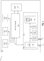
- an exemplary system-on-a-chip (e.g., SoC 202) includes multiple central processing units (i.e., CPUs, e.g., CPU0 204, CPU1, 206, CPUN 208), which issue memory requests through interface A to a hierarchical integrated memory controller (e.g., hierarchical integrated memory controller 230).
- Hierarchical integrated memory controller 230 enforces system coherence and serves as a conduit to a shared memory space (e.g., memory 214).
- memory 214 is a double data-rate-two or double-data-rate-three synchronous dynamic random access memory (i.e., DDR2/3 DRAM), although other suitable memory structures may be used.
- An I/O engine (e.g., I/O engine 216) issues memory requests and receives responses from the integrated memory controller through interface B.
- Both CPU and direct memory access (i.e., DMA) requests from the I/O engine must be coherent with the CPU requests. Accordingly, the CPU and DMA requests are merged at a system coherence point in hierarchical integrated memory controller 230 before being issued to a memory controller (e.g., memory controller 213) via interface C.
- hierarchical integrated memory controller 230 includes logic that analyzes incoming memory requests from the CPUs and the I/O engine to predict future memory accesses and issue speculative memory read requests (i.e., prefetches) to the memory controller through interface F. Requests issued through interfaces C and F are coherent memory streams.
- SoC 202 includes a specialized processing unit, e.g., graphics processing unit 240, which is a dedicated graphics rendering device that efficiently manipulates computer graphics information.
- graphics processing unit 240 i.e., GPU 240
- memory requesting agents e.g., GC0 218, GC1 220, GCN 222
- GPU 240 may include any suitable number of memory requesting agents.
- a graphics memory request scheduler e.g., graphics memory arbiter 224) combines non-coherent memory requests from different requesting agents into a single non-coherent stream of requests.
- the graphics memory arbiter 224 issues those requests from the single non-coherent stream to memory controller 213 via interface D.
- Hierarchical integrated memory controller 230 implements a hierarchical memory request stream arbitration technique.
- Hierarchical integrated memory controller 230 merges multiple coherent memory request streams from multiple memory request sources and arbitrates the merged coherent memory request stream with requests from a non-coherent memory request stream.
- Hierarchical integrated memory controller 230 merges memory request streams based on properties associated with individual memory request streams.
- coherent memory requests from the CPUs or from the I/O engine on interface C do not require peak memory bandwidth.
- those coherent memory requests typically do not generate predictable bank read/write access patterns. That is, CPU and I/O read or write requests typically have random arrival rates and access multiple memory banks simultaneously.
- Graphics processing unit 240 is a high bandwidth request source.
- memory controller 213 merges requests from interfaces C and D to increase memory bus utilization for bandwidth sensitive requestors and to reduce the average latency for latency sensitive requestors.
- a second set of scheduling policies is applied to each of the merged coherent memory request stream and a merged non-coherent memory request stream that are intended to increase bandwidth on the memory bus and reduce latency experienced by certain request types and/or request sources.
- hierarchical integrated memory controller 230 handles the non-coherent memory requests from GPU 240 differently from the coherent memory requests, e.g., to guarantee screen update without flicker.
- hierarchical integrated memory controller 230 uses an arbitration scheme that treats coherent and non-coherent request sources as separate entities and uses feedback to influence intra-source arbitration. For example, a next memory request issued to a merged memory request queue is determined using knowledge of the global pick, i.e., an indicator of the most recent memory request issued to the merged memory request queue, e.g., communicated to GPU 240 via interface H. Feedback regarding memory system bank status from a final arbitration stage is used by both the coherent request sources and the non-coherent request source to influence picking requests from their respective request queues.
- the memory bank status information increases the ability of a graphics memory arbiter (e.g., graphics memory arbiter 224) to select requests that result in page hits from requests in its internal queues.
- hierarchical integrated memory controller 230 uses page ownership rules to reduce a number of page conflicts on memory bus 215. In at least one embodiment, hierarchical integrated memory controller 230 uses bus turnaround rules to decrease the penalties incurred on a memory bus when switching the data bus from a read transaction to a write transaction and vice versa. In at least one embodiment, hierarchical integrated memory controller 230 uses limits on outstanding memory bandwidth to any particular request source to thereby provide an upper limit on the service time experienced by other memory requestors in the system.
- memory controller 213 includes a hierarchical merge multiplexer.
- hierarchical merge multiplexer 302 merges streams received from interfaces C, F, and D into a single unified stream of memory requests (e.g., merged memory request stream 316), which are queued in the merged memory request register (i.e., MRGQ) for issuance to memory 214 by memory controller 213 via memory bus 215.
- MRGQ merged memory request register
- SoC 202 includes multiple memory channels (not shown). Accordingly, a corresponding hierarchical merge multiplexer and a corresponding MRGQ are included for each memory channel.
- Memory request streams C, F, and D include memory channel information and memory requests are demultiplexed to individual hierarchical merge multiplexers and MRGQs according to the memory channel information included in individual memory requests.
- multiplexers 308, 320, and 312 receive corresponding select signals from respective arbitration logic, e.g., ARBSEL 304, ARBSEL 324, and ARBSEL 326, respectively.
- ARBSEL 304 controls the selection of coherent requests by multiplexer 308, e.g., from CPU or I/O requests from interface C, speculative coherent requests from interface F, and queued coherent requests from state element 318.
- ARBSEL 304 and the graphics memory arbiter 224 schedule requests to achieve as many page hits as possible based on memory bank status provided by memory page table 306, which includes information regarding previous memory requests selected for placement in the merged memory request queue (MRGQ).
- Memory page table 306 maintains an open or closed status for all chip-selects and banks in memory system 214. For open pages of memory system 214, memory page table 306 includes an identifier of which row of the page is open.
- a corresponding chip-select and bank status is updated in memory page table 306 based on an indicator of the memory request selected for placement in the merged memory request queue (e.g., signal 335).
- graphics memory arbiter 224 receives an indicator of memory requests selected for placement in the merged memory request queue, which is stored in block 334.
- the following information is provided to graphics memory arbiter 224 over interface E.
- both a front-end request stream i.e., request stream 311), which is based on the requests selected by multiplexer 308, and the GPU request stream are able to issue requests that favor page hits over page misses and over page conflicts.
- ARBSEL 324 controls the selection of requests by multiplexer 320 from at least a portion of the contents of retry queue RBDQ 328. Any suitable selection technique may be used (e.g., first-in-first-out, oldest ready, techniques based on page status and priority to increase bandwidth and decrease latency, etc.).
- state element 318 stores the output of multiplexer 320 to provide suitable timing characteristics.
- each request of a request stream provided to multiplexer 312 is associated with a priority value (e.g., urgent, high, medium, or low).
- ARBSEL 326 implements an additional priority policy based on general characteristics of input request streams received by multiplexer 312. For example, CPU and I/O requests have greater sensitivity to latency and limited bandwidth requests as compared to GPU requests, which typically require greater bandwidth and have lower sensitivity to latency. Therefore, in at least one embodiment, ARBSEL 326 prioritizes requests in request stream 311 over GPU requests of equal priority in request stream 329. In at least one embodiment, ARBSEL 326 enforces priority in the following order: urgent request stream 329, high request stream 311, high request stream 329, medium request stream 311, medium request stream 329, low request stream 311, and low request stream 329.
- control blocks 310 and 327 determine eligibility of requests from multiplexer 308 and queue 332, respectively, based on page ownership, read/write turnaround, and bandwidth control policies. Note that one or more other policies may be implemented by control blocks 310 and 327. Control blocks 310 and 327 determine the eligibility for arbitration of memory requests received from interfaces C, F, and D according to data received from memory page table 306 corresponding to those memory requests. If eligible for arbitration, requests selected by multiplexer 308 are forwarded to multiplexer 312 in request stream 311.
- hierarchical merge multiplexer 302 if a request selected by multiplexer 308 is not eligible for arbitration, the request is not provided to multiplexer 308 on the request stream 311 line, but rather is stored in retry queue RBDQ 328. If eligible for arbitration, the request from queue 332 is forwarded to multiplexer 312 as the request stream 329. If the request from queue 332 is not eligible for arbitration, the request is not provided to multiplexer 312 on the request stream 329 line, but rather remains in queue 332.
- control block 327 attempts to reduce the number of page conflicts issued to the memory bus. For example, control block 327 prevents a request sequence that allows a CPU to open and read from page 0 in a chip-select and bank pair and then let the GPU close page 0 and open and read from page 1 to the same chip-select and bank pair, and then allow a CPU to close page 1 and read from page 0 again. That sequence schedules repeated page conflicts on the memory bus.
- control block 327 tracks the source that last opened the page for each chip-select and bank pairs in the memory channel and stores this information in memory page table 306.
- a request source that is not the owner of the bank e.g., a CPU was the last source to open the page in memory page table 306
- control block 327 applies a set of rules that is used to decide when an ownership change is allowed.
- a source is able to assert ownership of a page for a longer period of time in the presence of outstanding page conflicts from another source, thereby issuing more page hits from the old source before turning to the new source to make forward progress.
- control block 327 implements page ownership rules that are based on source priority and current page owner. For example, when CPU or I/O is the owner of a memory page, a programmable timer is used to bind that page to the CPU or I/O for a period of time. A cycle count used to determine the period of time varies according to the priority of the conflicting GPU request. For example, three sets of counters may be used, e.g., one counter is used for each of high, medium, and low priority GPU requests, with increased cycle count values for each request type. An urgent memory request causes the CPU to immediately relinquish ownership of the page.
- a counter is started when a page owner first opens a page and the counter is not extended when that first page owner continues to have page hits to the open row.
- a time window that a conflicting (e.g., GPU) request must wait before it can open a page that is already opened to a different row by another requestor (e.g., CPU) is programmable for different priority levels (e.g., low, medium, high, and urgent priority levels).
- hierarchical merge multiplexer 302 when a GPU is the owner of a memory page, ownership is released when one of a variety of events occurs. For example, the ownership is released when a programmable number of requests of a given size and priority from GPU 240 has completed on the memory bus. That number of requests may vary with the priority (e.g., low, medium, or high) of the conflicting request (e.g., a request in request queue 311). The ownership may be released when the GPU asserts an end of burst indication indicating that the burst of requests to the page is completed.
- Hierarchical merge multiplexer 302 includes a set of counters depending on the priority of the blocked request. Note that the page ownership rules described herein are exemplary, and other embodiments of a hierarchical merge multiplexer may use other suitable page ownership rules.
- a bus turnaround occurs when a transaction of a first type (e.g., read or write) is followed by a transaction of a second type (e.g., write or read, respectively). Bus turnarounds can create multiple bubbles (i.e., penalties of multiple idle cycles) on the memory data bus due to timing parameters (e.g., DDR DIMM timing parameters for DRAM). Note that different memory speeds may have different bus turnaround times.
- ARBSEL 326 configures multiplexer 312 to merge traffic in a manner that reduces read-to-write and write-to-read bus turnarounds on the memory bus.
- ARBSEL 326 groups together read issuances separately from write issuances to reduce the number of bus turnarounds.
- Control block 327 keeps track of the current direction of the memory bus and when a requestor tries to change the direction of the bus, it has to wait for the particular time window to expire before it can be considered as an eligible requestor.
- control block 327 includes configuration registers corresponding to each traffic class that determine the timer window and specify when the particular traffic class must wait before it can turn around the bus.
- Exemplary configuration registers include an indicator of a number of control clocks or a number of bytes transferred that must occur before the particular traffic class can turn around the bus. Note that the bus turnaround rules described herein are exemplary, and other embodiments of a hierarchical merge multiplexer may use other suitable bus turnaround rules.
- SoC 202 limits the number of outstanding commands in the MRGQ from any given source. This is accomplished by maintaining counters on a per request source basis. In at least one embodiment of SoC 202, requests from interface C are limited, e.g., to a first number of bytes. Meanwhile, requests from interface D range up to a second number of bytes. Each time multiplexer 312 grants the bus to a request source, the corresponding counter is updated with the total number of bytes that are outstanding on the memory bus from that source. If a requestor presents a request when the counter for that source has exceeded the programmed threshold value, then the requestor is throttled back from being eligible for multiplexer 312 arbitration.
- This policy may enforce an upper limit for the latency seen from any other request source.
- request source bandwidth control ensures that display requests are serviced in a bounded amount of time.
- two sets of configuration registers control the number of maximum byte read or write requests outstanding in the MRGQ.
- separate throttle configuration registers which are activated from each source, may be included for reads and writes.
- GPU requests are generally considered non-coherent requests and frequently require high memory bandwidth.
- the GPU selects a best available request and provides it to hierarchical merge multiplexer 302 via interface D.
- Hierarchical merge multiplexer 302 stores the requests from the GPU in queue 332.
- request stream 311 is selected independently from the graphics memory arbiter selection and that the selected graphics memory arbiter request has direct access to the multiplexer 312, which is the final selection stage.
- SoC 202 rather than at a system serialization point (e.g., the input of DRAM controller 130 of SoC 102 of Fig.
- SoC 102 used by other memory request selection techniques, a high bandwidth GPU client achieves improved throughput over the throughput of SoC 102.
- System-on-a-chip 202 has improved throughput over SoC 102 because DRAM controller 130 re-orders the highly regular pattern of requests generated by the GPU into a lengthy pipeline.
- the requests generated by GPU 140 lose their page locality.
- the SoC 102 requires additional resources in the traffic arbitration blocks of the integrated memory controller.
- SoC 102 of Fig. 1 requires additional buffering in the GPU, as compared to SoC 202 of Figs. 2 and 3 .
- the SoC of Figs. 2 and 3 is not a unified queuing structure, i.e., requests from CPU, I/O, and GPU are not selected out of a single queue.
- an SoC implementing the techniques described in Figs. 2 and 3 can be physically partitioned to keep top-level modules, e.g., GPU and related sub-blocks, separate from other integrated memory controller logic.
- different top-level modules in SoC 202 can be clocked at different speeds, can implement different queuing structures to interface with each GPU client, and can have control and data path be independent of traffic arbitration and coherence pipelines in the front-end of the integrated memory controller.
- hierarchical integrated memory controller 230 operates using a control clock signal having a first frequency and GPU 240 operates using a control clock signal having a second frequency different from the first frequency.
- the graphics memory arbiter 224 can be independently verified and independently designed (e.g., logically and physically designed). The definitive boundaries for the top-level modules result in quicker integration of all top-level modules of the SoC.
- embodiments of the present invention may include software, data processing hardware, data processing system-implemented methods, and various processing operations, as described herein.
Landscapes
- Engineering & Computer Science (AREA)
- Theoretical Computer Science (AREA)
- Physics & Mathematics (AREA)
- General Engineering & Computer Science (AREA)
- General Physics & Mathematics (AREA)
- Human Computer Interaction (AREA)
- Memory System (AREA)
- Storage Device Security (AREA)
Claims (15)
- Verfahren zum Erstellen eines zusammengeführten Speicheranforderungsstromes (316) aus einer Vielzahl von Speicheranfrageströme, das Folgendes umfasst:Zusammenführen von kohärenten Speicheranforderungen in einen ersten seriellen Speicheranforderungsstrom; undAuswählen, durch einen Speichersteuerungsschaltkreis (213, 302), einer Speicheranforderung zum Platzieren im zusammengeführten Speicheranforderungsstrom aus mindestens dem ersten seriellen Speicheranforderungsstromes und einem zusammengeführten, nicht-kohärenten Speicheranforderungsstrom, wobei der zusammengeführte, nicht-kohärente Speicheranforderungsstrom mindestens zum Teil auf einem Indikator einer vorherigen Speicheranforderung basiert, die zur Platzierung im zusammengeführten Speicheranforderungsstrom (334) ausgewählt wurde.
- Verfahren nach Anspruch 1, wobei die Speicheranforderung, die zum Platzieren im zusammengeführten Speicheranforderungsstrom ausgewählt wurde, mindestens zum Teil auf Grundlage von Bus-Umkehrrichtlinien, Bandbreitenzuordnungsrichtlinien und Seiteneigentumsrichtlinien ausgewählt ist.
- Verfahren nach Anspruch 1, das ferner Folgendes umfasst:Auswählen einer Speicheranforderung zum Platzieren im ersten seriellen Speicheranforderungsstrom aus mindestens einem ersten kohärenten Speicheranforderungsstrom und einem zweiten kohärenten Speicheranforderungsstrom, wobei der zweite kohärente Speicheranforderungsstrom ein spekulativer kohärenter Anforderungsstrom ist.
- Verfahren nach Anspruch 1, das ferner Folgendes umfasst:Zusammenführen eines ersten kohärenten Speicheranforderungsstromes, eines zweiten kohärenten Speicheranforderungsstromes und eines erneuten Anforderungsstromes in den ersten seriellen Speicheranforderungsstrom.
- Verfahren nach Anspruch 1, das ferner Folgendes umfasst:Zusammenführen von nicht-kohärenten Speicheranforderungen in den zusammengeführten, nicht-kohärenten Speicheranforderungsstrom zumindest zum Teil auf Grundlage vom Indikator der vorherigen Speicheranforderung, die zur Platzierung im zusammengeführten Speicheranforderungsstrom ausgewählt ist.
- Vorrichtung, die Folgendes umfasst:eine Arbitrierungseinheit (210), die dazu ausgelegt ist, eine Vielzahl von kohärenten Speicheranforderungsströmen, die von einer ersten Vielzahl von Speicheranforderungsagenten (204, 206, 208, 216) empfangen wurde, mit dem mindestens einen kohärenten Speicheranforderungsstrom zusammenzuführen; undeine Speichersteuerungseinheit (213), die dazu ausgelegt ist, eine Speicheranfrage zum Platzieren in einem zusammengeführten Speicheranforderungsstrom (316) aus einem zusammengeführten, nicht-kohärenten Speicheranforderungsstrom auszuwählen, und einen ersten seriellen Speicheranforderungsstrom auf Grundlage des ersten kohärenten Speicheranforderungsstromes, wobei der zusammengeführte, nicht-kohärente Speicheranforderungsstrom mindestens zum Teil auf einem Indikator einer vorherigen Speicheranforderung basiert, die zum Platzieren im zusammengeführten Speicheranforderungsstrom (334) ausgewählt ist.
- Vorrichtung nach Anspruch 6, wobei die Speicheranforderung, die zum Platzieren im zusammengeführten Speicheranforderungsstrom gewählt ist, mindestens zum Teil auf Grundlage von einer oder mehrerer Bus-Umkehrrichtlinien, einer Bandbreitenzuordnungsrichtlinie und einer Seiteneigentumsrichtlinie gewählt ist.
- Vorrichtung nach Anspruch 6
wobei die Arbitrierungseinheit dazu ausgelegt ist, spekulative Speicheranfragen zu erzeugen und dazu ausgelegt ist, spekulative Speicheranfragen an die Speichersteuerungseinheit zu senden, die mit den ersten kohärenten Speicheranfragen kohärent sind, und wobei die Speichersteuerungseinheit eine Zusammenführungs-Multiplexereinheit umfasst, die dazu ausgelegt ist, um die ersten kohärenten Speicheranforderungen, die spekulativen Speicheranforderungen und nicht-kohärenten Speicheranforderungen hierarchisch in den zusammengeführten Speicheranforderungsstrom zusammenzuführen. - Vorrichtung nach Anspruch 8, wobei die Zusammenführungs-Multiplexereinheit Folgendes umfasst:eine erste Multiplexereinheit, die dazu ausgelegt ist, Anforderungen als Frontspeicher aus den ersten kohärenten Speicheranforderungen, den spekulativen Speicheranforderungen und einem dritten Satz von Speicheranforderungen zu wählen; undeine zweite Multiplexereinheit, die dazu ausgelegt ist, den dritten Satz von Speicheranforderungen aus den gespeicherten Versionen der Frontspeicheranfragen zu wählen.
- Vorrichtung nach Anspruch 8, wobei die Zusammenführungs-Multiplexereinheit Folgendes umfasst:eine dritte Multiplexereinheit, die dazu ausgelegt ist, die Speicheranforderungen zum Platzieren im zusammengeführten Speicheranforderungsstrom aus den Frontspeicheranforderungen, den nicht-kohärenten Speicheranforderungen und einem Auslass einer Speicherseitentabelle zu wählen.
- Vorrichtung nach Anspruch 6, wobei die erste Vielzahl von Speicheranforderungsagenten Folgendes umfasst:eine Vielzahl von Mehrzweck-Verarbeitungseinheiten, die dazu ausgelegt sind, eine Vielzahl von ersten kohärenten Speicheranforderungen zu erteilen; undeine Einlass-/Auslassprozessoreinheit, die dazu ausgelegt ist, zweite kohärente Speicheranforderungen zu erteilen.
- Vorrichtung nach Anspruch 6, wobei nicht-kohärente Speicheranfrageströme von einer Vielzahl von spezialisierten Prozessoreinheiten erzeugt werden, mindestens zum Teil auf Grundlage des Indikators der vorherigen Speicheranforderung, die zum Platzieren im zusammengeführten Speicheranfragestrom gewählt ist, und wobei der Indikator der vorherigen Speicheranfrage, die zum Platzieren im zusammengeführten Speicheranfragestrom gewählt ist, einen oder mehrere eines Chip-Auswahlindikators, eines Speicherbankindikators, eines Befehlsindikators, eines Zeilenindikators und eines Quellenindikators beinhaltet.
- Vorrichtung nach Anspruch 6, die ferner Folgendes umfasst:die erste Vielzahl von kohärenten Speicheranforderungsagenten, die dazu ausgelegt ist, die Vielzahl von kohärenten Speicheranforderungsströmen zu erteilen;eine Grafikprozessoreinheit (240), die dazu ausgelegt ist, mindestens einen kohärenten Anforderungsstrom und mindestens einen nicht-kohärenten Speicheranforderungsstrom zu erteilen, die Folgendes umfasst:ein Einlass-/Auslasstriebwerk (216), das dazu ausgelegt ist den mindestens einen kohärenten Speicheranforderungsstrom zu erteilen; undeinen Grafikspeicherarbitrierer (224), der dazu ausgelegt ist, den zusammengeführten, nicht-kohärenten Anforderungsstrom mindestens zum Teil auf Grundlage eines Indikators einer vorherigen Speicheranforderung zu erteilen, die zum Platzieren im zusammengeführten Speicheranforderungsstrom (334) gewählt ist;eine integrierte Speichersteuerung (230), die die Arbitrierereinheit und die Speichersteuerungseinheit umfasst, wobei die integrierte Speichersteuerung dazu ausgelegt ist, die Speichersteuerungen hierarchisch zu arbitrieren und den Speicheranforderungsstrom (316) aus der Vielzahl von kohärenten Speicheranforderungsströmen, dem mindestens einen Speicheranforderungsstrom, und dem zusammengeführten nicht-kohärenten Anforderungsstrom zu erzeugen.
- Vorrichtung nach Anspruch 13, wobei die Arbitrierungseinheit ferner dazu ausgelegt ist, die Vielzahl von kohärenten Speicheranforderungsströme und den mindestens einen kohärenten Speicheranforderungsstrom in mindestens den ersten kohärenten Speicheranforderungsstrom zusammenzuführen.
- Vorrichtung nach Anspruch 13, wobei die integrierte Speichersteuerung durch Verwenden eines Steuertaktsignales tätig ist, das eine erste Frequenz aufweist, und wobei die Grafikprozesseinheit durch Verwenden eines Steuertaktsignales tätig ist, das eine zweite Frequenz aufweist, wobei die zweite Frequenz unterschiedlich zu der ersten Frequenz ist.
Applications Claiming Priority (2)
| Application Number | Priority Date | Filing Date | Title |
|---|---|---|---|
| US12/431,874 US8266389B2 (en) | 2009-04-29 | 2009-04-29 | Hierarchical memory arbitration technique for disparate sources |
| PCT/US2010/032343 WO2010126810A1 (en) | 2009-04-29 | 2010-04-26 | Hierarchical memory arbitration technique for disparate sources |
Publications (3)
| Publication Number | Publication Date |
|---|---|
| EP2430554A1 EP2430554A1 (de) | 2012-03-21 |
| EP2430554B1 true EP2430554B1 (de) | 2018-03-14 |
| EP2430554B8 EP2430554B8 (de) | 2018-06-27 |
Family
ID=42316017
Family Applications (1)
| Application Number | Title | Priority Date | Filing Date |
|---|---|---|---|
| EP10716222.4A Active EP2430554B8 (de) | 2009-04-29 | 2010-04-26 | Hierarchisches speicherarbitrierungsverfahren für ungleiche quellen |
Country Status (6)
| Country | Link |
|---|---|
| US (2) | US8266389B2 (de) |
| EP (1) | EP2430554B8 (de) |
| JP (1) | JP5616435B2 (de) |
| KR (1) | KR101557090B1 (de) |
| CN (1) | CN102414671B (de) |
| WO (1) | WO2010126810A1 (de) |
Families Citing this family (34)
| Publication number | Priority date | Publication date | Assignee | Title |
|---|---|---|---|---|
| US8266389B2 (en) * | 2009-04-29 | 2012-09-11 | Advanced Micro Devices, Inc. | Hierarchical memory arbitration technique for disparate sources |
| US20120179883A1 (en) * | 2011-01-12 | 2012-07-12 | Broadcom Corpotation | System and method for dynamically adjusting memory performance |
| US9032162B1 (en) | 2011-08-12 | 2015-05-12 | Altera Corporation | Systems and methods for providing memory controllers with memory access request merging capabilities |
| US9176913B2 (en) | 2011-09-07 | 2015-11-03 | Apple Inc. | Coherence switch for I/O traffic |
| KR101949382B1 (ko) * | 2012-04-04 | 2019-02-18 | 삼성전자주식회사 | 서비스 품질의 향상을 위한 시스템 온 칩 및 시스템 온 칩의 제어 방법 |
| US8990473B2 (en) * | 2012-10-04 | 2015-03-24 | Applied Micro Circuits Corporation | Managing requests to open and closed banks in a memory system |
| US9110795B2 (en) | 2012-12-10 | 2015-08-18 | Qualcomm Incorporated | System and method for dynamically allocating memory in a memory subsystem having asymmetric memory components |
| US9092327B2 (en) | 2012-12-10 | 2015-07-28 | Qualcomm Incorporated | System and method for allocating memory to dissimilar memory devices using quality of service |
| US8959298B2 (en) | 2012-12-10 | 2015-02-17 | Qualcomm Incorporated | System and method for managing performance of a computing device having dissimilar memory types |
| US9075952B2 (en) * | 2013-01-17 | 2015-07-07 | Intel Corporation | Controlling bandwidth allocations in a system on a chip (SoC) |
| US10929551B2 (en) * | 2013-03-13 | 2021-02-23 | Comcast Cable Communications, Llc | Methods and systems for managing data assets |
| WO2014178846A1 (en) * | 2013-04-30 | 2014-11-06 | Hewlett-Packard Development Company, L.P. | Coalescing memory access requests |
| CN105579959B (zh) * | 2013-09-24 | 2019-06-07 | 渥太华大学 | 硬件加速器虚拟化 |
| WO2015067295A1 (en) | 2013-11-05 | 2015-05-14 | Huawei Technologies Co., Ltd. | Method and arrangement for controlling requests to a shared electronic resource |
| US9367491B2 (en) * | 2013-12-31 | 2016-06-14 | Global Unichip, Corp. | Method and apparatus for on-the-fly learning traffic control scheme |
| CN104581172A (zh) * | 2014-12-08 | 2015-04-29 | 北京中星微电子有限公司 | 一种实现svc宏块级算法的硬件结构 |
| US9886934B2 (en) * | 2014-12-24 | 2018-02-06 | Intel Corporation | Ordering mechanism for offload graphics scheduling |
| US10417146B1 (en) | 2018-05-15 | 2019-09-17 | Apple Inc. | Real-time resource handling in resource retry queue |
| US10866892B2 (en) | 2018-08-13 | 2020-12-15 | Apple Inc. | Establishing dependency in a resource retry queue |
| US11470017B2 (en) * | 2019-07-30 | 2022-10-11 | At&T Intellectual Property I, L.P. | Immersive reality component management via a reduced competition core network component |
| US11513973B2 (en) * | 2019-12-20 | 2022-11-29 | Advanced Micro Devices, Inc. | Arbitration scheme for coherent and non-coherent memory requests |
| US20210200694A1 (en) * | 2019-12-27 | 2021-07-01 | Advanced Micro Devices, Inc. | Staging buffer arbitration |
| CN111540198B (zh) * | 2020-04-17 | 2021-07-27 | 浙江工业大学 | 基于有向图卷积神经网络的城市交通态势识别方法 |
| KR102607421B1 (ko) * | 2020-04-27 | 2023-11-29 | 한국전자통신연구원 | 광 회선을 통해 상호 연결된 컴퓨팅 자원 분할 협업 시스템, 자원 분할 협업 방법 |
| CN111862592B (zh) * | 2020-05-27 | 2021-12-17 | 浙江工业大学 | 一种基于rgcn的交通流预测方法 |
| US12032500B2 (en) * | 2020-09-16 | 2024-07-09 | Intel Corporation | System, apparatus and method for controlling traffic in a fabric |
| CN112419718B (zh) * | 2020-11-17 | 2022-02-01 | 东北大学秦皇岛分校 | 一种基于时空图卷积神经网络的交通拥塞传播预测方法 |
| CN112650697B (zh) * | 2020-12-24 | 2023-04-18 | 西安翔腾微电子科技有限公司 | 一种基于ddr3存储控制器接口的多个主设备的仲裁电路 |
| US12353329B2 (en) * | 2021-12-22 | 2025-07-08 | Intel Corporation | System, apparatus and methods for direct data reads from memory |
| CN114416397B (zh) * | 2021-12-30 | 2025-12-05 | 上海阵量智能科技有限公司 | 一种芯片、访问内存的方法及计算机设备 |
| US12572280B2 (en) * | 2022-09-01 | 2026-03-10 | Advanced Micro Devices, Inc. | Memory controller and near-memory support for sparse accesses |
| CN116737617B (zh) * | 2023-08-11 | 2023-12-29 | 上海芯高峰微电子有限公司 | 一种访问控制器 |
| CN118708507B (zh) * | 2024-08-28 | 2025-01-17 | 珠海全志科技股份有限公司 | 应用于SoC系统的CPU访存优化控制方法及系统 |
| US20260079713A1 (en) * | 2024-09-17 | 2026-03-19 | Advanced Micro Devices, Inc. | Parallel processing memory traffic aggregation |
Family Cites Families (9)
| Publication number | Priority date | Publication date | Assignee | Title |
|---|---|---|---|---|
| US3665415A (en) * | 1970-04-29 | 1972-05-23 | Honeywell Inf Systems | Data processing system with program interrupt priority apparatus utilizing working store for multiplexing interrupt requests |
| US6092158A (en) * | 1997-06-13 | 2000-07-18 | Intel Corporation | Method and apparatus for arbitrating between command streams |
| US6487640B1 (en) * | 1999-01-19 | 2002-11-26 | International Business Machines Corporation | Memory access request reordering to reduce memory access latency |
| US6625700B2 (en) * | 2001-05-31 | 2003-09-23 | Sun Microsystems, Inc. | Arbitration and select logic for accessing a shared memory |
| US20030158985A1 (en) * | 2002-02-15 | 2003-08-21 | Edward Fried | Systems and methods for fair arbitration between multiple request signals |
| US7133972B2 (en) * | 2002-06-07 | 2006-11-07 | Micron Technology, Inc. | Memory hub with internal cache and/or memory access prediction |
| US7210018B2 (en) * | 2002-12-30 | 2007-04-24 | International Business Machines Corporation | Multiple-stage pipeline for transaction conversion |
| US7698498B2 (en) * | 2005-12-29 | 2010-04-13 | Intel Corporation | Memory controller with bank sorting and scheduling |
| US8266389B2 (en) * | 2009-04-29 | 2012-09-11 | Advanced Micro Devices, Inc. | Hierarchical memory arbitration technique for disparate sources |
-
2009
- 2009-04-29 US US12/431,874 patent/US8266389B2/en active Active
-
2010
- 2010-04-26 CN CN201080018676.3A patent/CN102414671B/zh active Active
- 2010-04-26 KR KR1020117028602A patent/KR101557090B1/ko not_active Expired - Fee Related
- 2010-04-26 EP EP10716222.4A patent/EP2430554B8/de active Active
- 2010-04-26 JP JP2012508559A patent/JP5616435B2/ja active Active
- 2010-04-26 WO PCT/US2010/032343 patent/WO2010126810A1/en not_active Ceased
-
2012
- 2012-08-31 US US13/600,614 patent/US8645639B2/en not_active Expired - Fee Related
Non-Patent Citations (1)
| Title |
|---|
| None * |
Also Published As
| Publication number | Publication date |
|---|---|
| US8645639B2 (en) | 2014-02-04 |
| KR101557090B1 (ko) | 2015-10-02 |
| US20120331226A1 (en) | 2012-12-27 |
| EP2430554A1 (de) | 2012-03-21 |
| CN102414671B (zh) | 2015-05-27 |
| JP2012525642A (ja) | 2012-10-22 |
| US8266389B2 (en) | 2012-09-11 |
| CN102414671A (zh) | 2012-04-11 |
| US20100281231A1 (en) | 2010-11-04 |
| KR20120014914A (ko) | 2012-02-20 |
| JP5616435B2 (ja) | 2014-10-29 |
| EP2430554B8 (de) | 2018-06-27 |
| WO2010126810A1 (en) | 2010-11-04 |
Similar Documents
| Publication | Publication Date | Title |
|---|---|---|
| US8266389B2 (en) | Hierarchical memory arbitration technique for disparate sources | |
| KR102728014B1 (ko) | 메모리 제어기에서의 리프레시 방식 | |
| US12282439B2 (en) | Dynamic page state aware scheduling of read/write burst transactions | |
| CN109564556B (zh) | 具有条纹和读取/写入事务管理的存储器控制器仲裁器 | |
| CN101305354B (zh) | 在多个请求之间进行仲裁的系统和方法 | |
| Akesson et al. | Predator: a predictable SDRAM memory controller | |
| JP6840145B2 (ja) | 高速メモリインタフェースのためのコマンドアービトレーション | |
| US8095744B2 (en) | Device for controlling access from a plurality of masters to shared memory composed of a plurality of banks each having a plurality of pages | |
| US8412870B2 (en) | Optimized arbiter using multi-level arbitration | |
| US6330645B1 (en) | Multi-stream coherent memory controller apparatus and method | |
| CN102402490A (zh) | 具有与业务类别关联的端口的多端口存储器控制器 | |
| JP2010282405A (ja) | データ処理システム | |
| WO2001048617A2 (en) | Prioritized bus request scheduling mechanism for processing devices | |
| JP2024512625A (ja) | アービトレーション中の書き込みバンクグループのマスク | |
| CN100565491C (zh) | 开关矩阵系统和高性能总线仲裁的方法 | |
| US8285892B2 (en) | Quantum burst arbiter and memory controller | |
| US9335934B2 (en) | Shared memory controller and method of using same | |
| EP3270294A1 (de) | Befehlsarbitrierung für hochgeschwindigkeitsspeicherschnittstellen | |
| US7130947B2 (en) | Method of arbitration which allows requestors from multiple frequency domains | |
| US12417791B2 (en) | Direct memory access (DMA) circuit and operation method thereof | |
| Liu et al. | Multi-bank memory access scheduler and scalability |
Legal Events
| Date | Code | Title | Description |
|---|---|---|---|
| PUAI | Public reference made under article 153(3) epc to a published international application that has entered the european phase |
Free format text: ORIGINAL CODE: 0009012 |
|
| 17P | Request for examination filed |
Effective date: 20111129 |
|
| AK | Designated contracting states |
Kind code of ref document: A1 Designated state(s): AT BE BG CH CY CZ DE DK EE ES FI FR GB GR HR HU IE IS IT LI LT LU LV MC MK MT NL NO PL PT RO SE SI SK SM TR |
|
| DAX | Request for extension of the european patent (deleted) | ||
| 17Q | First examination report despatched |
Effective date: 20150914 |
|
| GRAP | Despatch of communication of intention to grant a patent |
Free format text: ORIGINAL CODE: EPIDOSNIGR1 |
|
| INTG | Intention to grant announced |
Effective date: 20170817 |
|
| GRAS | Grant fee paid |
Free format text: ORIGINAL CODE: EPIDOSNIGR3 |
|
| GRAJ | Information related to disapproval of communication of intention to grant by the applicant or resumption of examination proceedings by the epo deleted |
Free format text: ORIGINAL CODE: EPIDOSDIGR1 |
|
| GRAL | Information related to payment of fee for publishing/printing deleted |
Free format text: ORIGINAL CODE: EPIDOSDIGR3 |
|
| GRAR | Information related to intention to grant a patent recorded |
Free format text: ORIGINAL CODE: EPIDOSNIGR71 |
|
| GRAA | (expected) grant |
Free format text: ORIGINAL CODE: 0009210 |
|
| INTC | Intention to grant announced (deleted) | ||
| AK | Designated contracting states |
Kind code of ref document: B1 Designated state(s): AT BE BG CH CY CZ DE DK EE ES FI FR GB GR HR HU IE IS IT LI LT LU LV MC MK MT NL NO PL PT RO SE SI SK SM TR |
|
| INTG | Intention to grant announced |
Effective date: 20180206 |
|
| REG | Reference to a national code |
Ref country code: GB Ref legal event code: FG4D |
|
| REG | Reference to a national code |
Ref country code: CH Ref legal event code: EP Ref country code: AT Ref legal event code: REF Ref document number: 979520 Country of ref document: AT Kind code of ref document: T Effective date: 20180315 |
|
| GRAT | Correction requested after decision to grant or after decision to maintain patent in amended form |
Free format text: ORIGINAL CODE: EPIDOSNCDEC |
|
| REG | Reference to a national code |
Ref country code: IE Ref legal event code: FG4D |
|
| REG | Reference to a national code |
Ref country code: DE Ref legal event code: R096 Ref document number: 602010049157 Country of ref document: DE |
|
| RAP2 | Party data changed (patent owner data changed or rights of a patent transferred) |
Owner name: ADVANCED MICRO DEVICES, INC. Owner name: ATI TECHNOLOGIES ULC |
|
| RAP2 | Party data changed (patent owner data changed or rights of a patent transferred) |
Owner name: ADVANCED MICRO DEVICES, INC. Owner name: ATI TECHNOLOGIES ULC |
|
| REG | Reference to a national code |
Ref country code: NL Ref legal event code: MP Effective date: 20180314 |
|
| REG | Reference to a national code |
Ref country code: LT Ref legal event code: MG4D |
|
| PG25 | Lapsed in a contracting state [announced via postgrant information from national office to epo] |
Ref country code: CY Free format text: LAPSE BECAUSE OF FAILURE TO SUBMIT A TRANSLATION OF THE DESCRIPTION OR TO PAY THE FEE WITHIN THE PRESCRIBED TIME-LIMIT Effective date: 20180314 Ref country code: FI Free format text: LAPSE BECAUSE OF FAILURE TO SUBMIT A TRANSLATION OF THE DESCRIPTION OR TO PAY THE FEE WITHIN THE PRESCRIBED TIME-LIMIT Effective date: 20180314 Ref country code: NO Free format text: LAPSE BECAUSE OF FAILURE TO SUBMIT A TRANSLATION OF THE DESCRIPTION OR TO PAY THE FEE WITHIN THE PRESCRIBED TIME-LIMIT Effective date: 20180614 Ref country code: HR Free format text: LAPSE BECAUSE OF FAILURE TO SUBMIT A TRANSLATION OF THE DESCRIPTION OR TO PAY THE FEE WITHIN THE PRESCRIBED TIME-LIMIT Effective date: 20180314 Ref country code: ES Free format text: LAPSE BECAUSE OF FAILURE TO SUBMIT A TRANSLATION OF THE DESCRIPTION OR TO PAY THE FEE WITHIN THE PRESCRIBED TIME-LIMIT Effective date: 20180314 Ref country code: LT Free format text: LAPSE BECAUSE OF FAILURE TO SUBMIT A TRANSLATION OF THE DESCRIPTION OR TO PAY THE FEE WITHIN THE PRESCRIBED TIME-LIMIT Effective date: 20180314 |
|
| REG | Reference to a national code |
Ref country code: AT Ref legal event code: MK05 Ref document number: 979520 Country of ref document: AT Kind code of ref document: T Effective date: 20180314 |
|
| PG25 | Lapsed in a contracting state [announced via postgrant information from national office to epo] |
Ref country code: SE Free format text: LAPSE BECAUSE OF FAILURE TO SUBMIT A TRANSLATION OF THE DESCRIPTION OR TO PAY THE FEE WITHIN THE PRESCRIBED TIME-LIMIT Effective date: 20180314 Ref country code: LV Free format text: LAPSE BECAUSE OF FAILURE TO SUBMIT A TRANSLATION OF THE DESCRIPTION OR TO PAY THE FEE WITHIN THE PRESCRIBED TIME-LIMIT Effective date: 20180314 Ref country code: BG Free format text: LAPSE BECAUSE OF FAILURE TO SUBMIT A TRANSLATION OF THE DESCRIPTION OR TO PAY THE FEE WITHIN THE PRESCRIBED TIME-LIMIT Effective date: 20180614 Ref country code: GR Free format text: LAPSE BECAUSE OF FAILURE TO SUBMIT A TRANSLATION OF THE DESCRIPTION OR TO PAY THE FEE WITHIN THE PRESCRIBED TIME-LIMIT Effective date: 20180615 |
|
| PG25 | Lapsed in a contracting state [announced via postgrant information from national office to epo] |
Ref country code: IT Free format text: LAPSE BECAUSE OF FAILURE TO SUBMIT A TRANSLATION OF THE DESCRIPTION OR TO PAY THE FEE WITHIN THE PRESCRIBED TIME-LIMIT Effective date: 20180314 Ref country code: NL Free format text: LAPSE BECAUSE OF FAILURE TO SUBMIT A TRANSLATION OF THE DESCRIPTION OR TO PAY THE FEE WITHIN THE PRESCRIBED TIME-LIMIT Effective date: 20180314 Ref country code: RO Free format text: LAPSE BECAUSE OF FAILURE TO SUBMIT A TRANSLATION OF THE DESCRIPTION OR TO PAY THE FEE WITHIN THE PRESCRIBED TIME-LIMIT Effective date: 20180314 Ref country code: PL Free format text: LAPSE BECAUSE OF FAILURE TO SUBMIT A TRANSLATION OF THE DESCRIPTION OR TO PAY THE FEE WITHIN THE PRESCRIBED TIME-LIMIT Effective date: 20180314 Ref country code: EE Free format text: LAPSE BECAUSE OF FAILURE TO SUBMIT A TRANSLATION OF THE DESCRIPTION OR TO PAY THE FEE WITHIN THE PRESCRIBED TIME-LIMIT Effective date: 20180314 |
|
| PG25 | Lapsed in a contracting state [announced via postgrant information from national office to epo] |
Ref country code: SM Free format text: LAPSE BECAUSE OF FAILURE TO SUBMIT A TRANSLATION OF THE DESCRIPTION OR TO PAY THE FEE WITHIN THE PRESCRIBED TIME-LIMIT Effective date: 20180314 Ref country code: SK Free format text: LAPSE BECAUSE OF FAILURE TO SUBMIT A TRANSLATION OF THE DESCRIPTION OR TO PAY THE FEE WITHIN THE PRESCRIBED TIME-LIMIT Effective date: 20180314 Ref country code: AT Free format text: LAPSE BECAUSE OF FAILURE TO SUBMIT A TRANSLATION OF THE DESCRIPTION OR TO PAY THE FEE WITHIN THE PRESCRIBED TIME-LIMIT Effective date: 20180314 Ref country code: CZ Free format text: LAPSE BECAUSE OF FAILURE TO SUBMIT A TRANSLATION OF THE DESCRIPTION OR TO PAY THE FEE WITHIN THE PRESCRIBED TIME-LIMIT Effective date: 20180314 |
|
| REG | Reference to a national code |
Ref country code: CH Ref legal event code: PL |
|
| REG | Reference to a national code |
Ref country code: DE Ref legal event code: R097 Ref document number: 602010049157 Country of ref document: DE |
|
| REG | Reference to a national code |
Ref country code: BE Ref legal event code: MM Effective date: 20180430 |
|
| PG25 | Lapsed in a contracting state [announced via postgrant information from national office to epo] |
Ref country code: PT Free format text: LAPSE BECAUSE OF FAILURE TO SUBMIT A TRANSLATION OF THE DESCRIPTION OR TO PAY THE FEE WITHIN THE PRESCRIBED TIME-LIMIT Effective date: 20180716 |
|
| PLBE | No opposition filed within time limit |
Free format text: ORIGINAL CODE: 0009261 |
|
| STAA | Information on the status of an ep patent application or granted ep patent |
Free format text: STATUS: NO OPPOSITION FILED WITHIN TIME LIMIT |
|
| REG | Reference to a national code |
Ref country code: IE Ref legal event code: MM4A |
|
| PG25 | Lapsed in a contracting state [announced via postgrant information from national office to epo] |
Ref country code: LU Free format text: LAPSE BECAUSE OF NON-PAYMENT OF DUE FEES Effective date: 20180426 Ref country code: MC Free format text: LAPSE BECAUSE OF FAILURE TO SUBMIT A TRANSLATION OF THE DESCRIPTION OR TO PAY THE FEE WITHIN THE PRESCRIBED TIME-LIMIT Effective date: 20180314 Ref country code: DK Free format text: LAPSE BECAUSE OF FAILURE TO SUBMIT A TRANSLATION OF THE DESCRIPTION OR TO PAY THE FEE WITHIN THE PRESCRIBED TIME-LIMIT Effective date: 20180314 |
|
| 26N | No opposition filed |
Effective date: 20181217 |
|
| PG25 | Lapsed in a contracting state [announced via postgrant information from national office to epo] |
Ref country code: SI Free format text: LAPSE BECAUSE OF FAILURE TO SUBMIT A TRANSLATION OF THE DESCRIPTION OR TO PAY THE FEE WITHIN THE PRESCRIBED TIME-LIMIT Effective date: 20180314 Ref country code: LI Free format text: LAPSE BECAUSE OF NON-PAYMENT OF DUE FEES Effective date: 20180430 Ref country code: CH Free format text: LAPSE BECAUSE OF NON-PAYMENT OF DUE FEES Effective date: 20180430 Ref country code: BE Free format text: LAPSE BECAUSE OF NON-PAYMENT OF DUE FEES Effective date: 20180430 |
|
| PG25 | Lapsed in a contracting state [announced via postgrant information from national office to epo] |
Ref country code: FR Free format text: LAPSE BECAUSE OF NON-PAYMENT OF DUE FEES Effective date: 20180514 Ref country code: IE Free format text: LAPSE BECAUSE OF NON-PAYMENT OF DUE FEES Effective date: 20180426 |
|
| PG25 | Lapsed in a contracting state [announced via postgrant information from national office to epo] |
Ref country code: MT Free format text: LAPSE BECAUSE OF NON-PAYMENT OF DUE FEES Effective date: 20180426 |
|
| PG25 | Lapsed in a contracting state [announced via postgrant information from national office to epo] |
Ref country code: TR Free format text: LAPSE BECAUSE OF FAILURE TO SUBMIT A TRANSLATION OF THE DESCRIPTION OR TO PAY THE FEE WITHIN THE PRESCRIBED TIME-LIMIT Effective date: 20180314 |
|
| PG25 | Lapsed in a contracting state [announced via postgrant information from national office to epo] |
Ref country code: HU Free format text: LAPSE BECAUSE OF FAILURE TO SUBMIT A TRANSLATION OF THE DESCRIPTION OR TO PAY THE FEE WITHIN THE PRESCRIBED TIME-LIMIT; INVALID AB INITIO Effective date: 20100426 |
|
| PG25 | Lapsed in a contracting state [announced via postgrant information from national office to epo] |
Ref country code: MK Free format text: LAPSE BECAUSE OF NON-PAYMENT OF DUE FEES Effective date: 20180314 |
|
| PG25 | Lapsed in a contracting state [announced via postgrant information from national office to epo] |
Ref country code: IS Free format text: LAPSE BECAUSE OF FAILURE TO SUBMIT A TRANSLATION OF THE DESCRIPTION OR TO PAY THE FEE WITHIN THE PRESCRIBED TIME-LIMIT Effective date: 20180714 |
|
| P01 | Opt-out of the competence of the unified patent court (upc) registered |
Effective date: 20230530 |
|
| PGFP | Annual fee paid to national office [announced via postgrant information from national office to epo] |
Ref country code: DE Payment date: 20250313 Year of fee payment: 16 |
|
| PGFP | Annual fee paid to national office [announced via postgrant information from national office to epo] |
Ref country code: GB Payment date: 20250415 Year of fee payment: 16 |