EP2426740A1 - Substrate retainer, electronic apparatus, and display apparatus - Google Patents
Substrate retainer, electronic apparatus, and display apparatus Download PDFInfo
- Publication number
- EP2426740A1 EP2426740A1 EP10769729A EP10769729A EP2426740A1 EP 2426740 A1 EP2426740 A1 EP 2426740A1 EP 10769729 A EP10769729 A EP 10769729A EP 10769729 A EP10769729 A EP 10769729A EP 2426740 A1 EP2426740 A1 EP 2426740A1
- Authority
- EP
- European Patent Office
- Prior art keywords
- light emitting
- emitting diode
- electronic device
- circuit boards
- boards
- Prior art date
- Legal status (The legal status is an assumption and is not a legal conclusion. Google has not performed a legal analysis and makes no representation as to the accuracy of the status listed.)
- Withdrawn
Links
- 239000000758 substrate Substances 0.000 title 1
- 230000008878 coupling Effects 0.000 claims abstract description 30
- 238000010168 coupling process Methods 0.000 claims abstract description 30
- 238000005859 coupling reaction Methods 0.000 claims abstract description 30
- 230000003287 optical effect Effects 0.000 claims description 17
- 230000003245 working effect Effects 0.000 description 20
- 230000000694 effects Effects 0.000 description 11
- 230000002093 peripheral effect Effects 0.000 description 10
- 238000003780 insertion Methods 0.000 description 9
- 230000037431 insertion Effects 0.000 description 9
- 238000000926 separation method Methods 0.000 description 7
- 239000000853 adhesive Substances 0.000 description 3
- 238000001579 optical reflectometry Methods 0.000 description 3
- 229920003002 synthetic resin Polymers 0.000 description 3
- 239000000057 synthetic resin Substances 0.000 description 3
- 229920000515 polycarbonate Polymers 0.000 description 2
- 239000004417 polycarbonate Substances 0.000 description 2
- 238000002310 reflectometry Methods 0.000 description 2
- 210000000078 claw Anatomy 0.000 description 1
- 230000001678 irradiating effect Effects 0.000 description 1
- 238000003475 lamination Methods 0.000 description 1
- 239000002184 metal Substances 0.000 description 1
- 238000000034 method Methods 0.000 description 1
- 230000000149 penetrating effect Effects 0.000 description 1
- 239000011295 pitch Substances 0.000 description 1
- 230000010287 polarization Effects 0.000 description 1
- 230000000630 rising effect Effects 0.000 description 1
- 238000007493 shaping process Methods 0.000 description 1
Images








Classifications
-
- H—ELECTRICITY
- H05—ELECTRIC TECHNIQUES NOT OTHERWISE PROVIDED FOR
- H05K—PRINTED CIRCUITS; CASINGS OR CONSTRUCTIONAL DETAILS OF ELECTRIC APPARATUS; MANUFACTURE OF ASSEMBLAGES OF ELECTRICAL COMPONENTS
- H05K1/00—Printed circuits
- H05K1/02—Details
- H05K1/14—Structural association of two or more printed circuits
- H05K1/142—Arrangements of planar printed circuit boards in the same plane, e.g. auxiliary printed circuit insert mounted in a main printed circuit
-
- G—PHYSICS
- G02—OPTICS
- G02F—OPTICAL DEVICES OR ARRANGEMENTS FOR THE CONTROL OF LIGHT BY MODIFICATION OF THE OPTICAL PROPERTIES OF THE MEDIA OF THE ELEMENTS INVOLVED THEREIN; NON-LINEAR OPTICS; FREQUENCY-CHANGING OF LIGHT; OPTICAL LOGIC ELEMENTS; OPTICAL ANALOGUE/DIGITAL CONVERTERS
- G02F1/00—Devices or arrangements for the control of the intensity, colour, phase, polarisation or direction of light arriving from an independent light source, e.g. switching, gating or modulating; Non-linear optics
- G02F1/01—Devices or arrangements for the control of the intensity, colour, phase, polarisation or direction of light arriving from an independent light source, e.g. switching, gating or modulating; Non-linear optics for the control of the intensity, phase, polarisation or colour
- G02F1/13—Devices or arrangements for the control of the intensity, colour, phase, polarisation or direction of light arriving from an independent light source, e.g. switching, gating or modulating; Non-linear optics for the control of the intensity, phase, polarisation or colour based on liquid crystals, e.g. single liquid crystal display cells
- G02F1/133—Constructional arrangements; Operation of liquid crystal cells; Circuit arrangements
- G02F1/1333—Constructional arrangements; Manufacturing methods
- G02F1/1335—Structural association of cells with optical devices, e.g. polarisers or reflectors
- G02F1/1336—Illuminating devices
- G02F1/133602—Direct backlight
- G02F1/133603—Direct backlight with LEDs
-
- G—PHYSICS
- G02—OPTICS
- G02F—OPTICAL DEVICES OR ARRANGEMENTS FOR THE CONTROL OF LIGHT BY MODIFICATION OF THE OPTICAL PROPERTIES OF THE MEDIA OF THE ELEMENTS INVOLVED THEREIN; NON-LINEAR OPTICS; FREQUENCY-CHANGING OF LIGHT; OPTICAL LOGIC ELEMENTS; OPTICAL ANALOGUE/DIGITAL CONVERTERS
- G02F1/00—Devices or arrangements for the control of the intensity, colour, phase, polarisation or direction of light arriving from an independent light source, e.g. switching, gating or modulating; Non-linear optics
- G02F1/01—Devices or arrangements for the control of the intensity, colour, phase, polarisation or direction of light arriving from an independent light source, e.g. switching, gating or modulating; Non-linear optics for the control of the intensity, phase, polarisation or colour
- G02F1/13—Devices or arrangements for the control of the intensity, colour, phase, polarisation or direction of light arriving from an independent light source, e.g. switching, gating or modulating; Non-linear optics for the control of the intensity, phase, polarisation or colour based on liquid crystals, e.g. single liquid crystal display cells
- G02F1/133—Constructional arrangements; Operation of liquid crystal cells; Circuit arrangements
- G02F1/1333—Constructional arrangements; Manufacturing methods
- G02F1/1335—Structural association of cells with optical devices, e.g. polarisers or reflectors
- G02F1/1336—Illuminating devices
- G02F1/133602—Direct backlight
- G02F1/133608—Direct backlight including particular frames or supporting means
-
- G—PHYSICS
- G02—OPTICS
- G02F—OPTICAL DEVICES OR ARRANGEMENTS FOR THE CONTROL OF LIGHT BY MODIFICATION OF THE OPTICAL PROPERTIES OF THE MEDIA OF THE ELEMENTS INVOLVED THEREIN; NON-LINEAR OPTICS; FREQUENCY-CHANGING OF LIGHT; OPTICAL LOGIC ELEMENTS; OPTICAL ANALOGUE/DIGITAL CONVERTERS
- G02F2201/00—Constructional arrangements not provided for in groups G02F1/00 - G02F7/00
- G02F2201/46—Fixing elements
- G02F2201/465—Snap -fit
-
- H—ELECTRICITY
- H05—ELECTRIC TECHNIQUES NOT OTHERWISE PROVIDED FOR
- H05K—PRINTED CIRCUITS; CASINGS OR CONSTRUCTIONAL DETAILS OF ELECTRIC APPARATUS; MANUFACTURE OF ASSEMBLAGES OF ELECTRICAL COMPONENTS
- H05K2201/00—Indexing scheme relating to printed circuits covered by H05K1/00
- H05K2201/03—Conductive materials
- H05K2201/0302—Properties and characteristics in general
- H05K2201/0311—Metallic part with specific elastic properties, e.g. bent piece of metal as electrical contact
-
- H—ELECTRICITY
- H05—ELECTRIC TECHNIQUES NOT OTHERWISE PROVIDED FOR
- H05K—PRINTED CIRCUITS; CASINGS OR CONSTRUCTIONAL DETAILS OF ELECTRIC APPARATUS; MANUFACTURE OF ASSEMBLAGES OF ELECTRICAL COMPONENTS
- H05K2201/00—Indexing scheme relating to printed circuits covered by H05K1/00
- H05K2201/09—Shape and layout
- H05K2201/09009—Substrate related
- H05K2201/09063—Holes or slots in insulating substrate not used for electrical connections
-
- H—ELECTRICITY
- H05—ELECTRIC TECHNIQUES NOT OTHERWISE PROVIDED FOR
- H05K—PRINTED CIRCUITS; CASINGS OR CONSTRUCTIONAL DETAILS OF ELECTRIC APPARATUS; MANUFACTURE OF ASSEMBLAGES OF ELECTRICAL COMPONENTS
- H05K2201/00—Indexing scheme relating to printed circuits covered by H05K1/00
- H05K2201/10—Details of components or other objects attached to or integrated in a printed circuit board
- H05K2201/10007—Types of components
- H05K2201/10106—Light emitting diode [LED]
-
- H—ELECTRICITY
- H05—ELECTRIC TECHNIQUES NOT OTHERWISE PROVIDED FOR
- H05K—PRINTED CIRCUITS; CASINGS OR CONSTRUCTIONAL DETAILS OF ELECTRIC APPARATUS; MANUFACTURE OF ASSEMBLAGES OF ELECTRICAL COMPONENTS
- H05K2201/00—Indexing scheme relating to printed circuits covered by H05K1/00
- H05K2201/10—Details of components or other objects attached to or integrated in a printed circuit board
- H05K2201/10007—Types of components
- H05K2201/10189—Non-printed connector
Definitions
- the present invention relates to a board holder that holds a plurality of circuit boards disposed in parallel, an electronic device having the board holder, and a display apparatus having the electronic device.
- an electronic device is disposed that has a light source for irradiating the display section.
- the electronic device is provided with, for example, a plurality of light emitting diode boards disposed in parallel and having a plurality of light emitting diodes mounted on one surface, a plurality of lenses that diverge the light emitted by the light emitting diodes, a lens cover that has through holes in which the lenses are disposed and sandwiches peripheral parts of the lenses with the light emitting diode boards, and a backlight frame that supports the light emitting diode boards disposed in parallel (see, for example, Patent Document 1).
- a plurality of insertion holes are formed in the light emitting diode boards and the lens cover, attachment holes corresponding to the insertion holes are formed in the backlight frame, and male screws inserted in the insertion holes of the light emitting diode boards and the lens cover are screwed into the attachment holes, whereby the light emitting diode boards and the lens cover are fixed to the backlight frame and the peripheral parts of the lenses are sandwiched between peripheral parts of the through holes in the lens cover and the light emitting diode boards to thereby fix the lenses.
- the present invention has been made with the aim of solving the above problems, and it is an object of the present invention to provide: a board holder capable of easily holding a plurality of circuit boards disposed in parallel, on a support member, without using a screw; an electronic device having the board holder; and a display apparatus having the electronic device.
- a board holder according to the present invention is a board holder that holds, on a support member for supporting a plurality of circuit boards disposed in parallel, the circuit boards, and is characterized by comprising: a plurality of protruding sections to be inserted in holes formed in an adjacent circuit boards and the support member; and a coupling section coupling the protruding sections.
- the adjacent circuit boards can be simultaneously held on the support member, the separation distances between the circuit boards can be made uniform, and the circuit boards can be secured in this condition, so that the workability of attachment of the circuit boards disposed in parallel onto the support member can be improved.
- the protruding sections of the board holder according to the present invention are arranged in a plurality of rows.
- the circuit boards in a plurality of rows can be simultaneously held on the support member, the separation distances between the circuit boards in a plurality of rows can be made uniform, and the circuit boards can be secured in this condition, so that the workability of attachment of the circuit boards disposed in parallel onto the support member can be improved.
- the coupling section of the board holder according to the present invention has an attachment section attached to the support member.
- the attachment section of the board holder can be attached to the support member, so that the circuit boards can be firmly secured without any increase in the number of parts.
- the coupling section of the board holder according to the present invention has a columnar section having an end contacting with a sheet surface of an optical sheet disposed facing to the circuit boards with a space therebetween, thereby limiting a bend of the optical sheet.
- a bend, toward the circuit board side, of the optical sheet disposed facing to the circuit boards with a space therebetween can be restrained by the columnar section without any increase in the number of parts, so that the optical characteristic by the optical sheet can be stabilized.
- the board holder according to the present invention has a connector between the protruding sections of the coupling section.
- the connector of the coupling section can be connected to the connecting sections of the adjacent circuit boards, in other words, the board holder itself constitutes the connector, so that the workability of connection of the circuit boards by the connector can be improved.
- the connector can be covered with the coupling section, so that the brightness characteristic can be improved.
- an electronic device is characterized by comprising: a plurality of circuit boards disposed in parallel and having a light emitting diode mounted thereon; and the above-described board holder.
- the adjacent circuit boards can be held on the support member, the separation distances between the circuit boards can be made uniform, and the circuit boards can be secured to the support member in this condition, so that the workability of attachment of the circuit boards disposed in parallel can be improved.
- the circuit boards are arranged in a plurality of rows.
- the circuit boards in a plurality of rows can be held on the support member, the separation distances between the circuit boards in a plurality of rows can be made uniform, and the circuit boards can be attached to the support member in this condition, so that the workability of attachment of the circuit boards disposed in parallel can be improved.
- a circuit section and the light emitting diode are disposed, and a connecting section for connecting the adjacent circuit boards together by the connector is provided on the one surface.
- the circuit boards each having the circuit section on one surface can be disposed in parallel in such a way that the other surfaces are two-dimensionally aligned, so that the thickness of the circuit board portion can be reduced and the electronic device can be reduced in thickness.
- the other surfaces of the circuit boards disposed in parallel can be brought close to the support member supporting the circuit boards without affected by the connectors, so that it is unnecessary to form through holes corresponding to the connectors in the support member and the dust-proofness of the circuit board portion can be improved.
- the connector is provided on the coupling section.
- the board holder itself constitutes the connector, so that it is not particularly necessary to operate the connector and the workability of connection of the circuit boards by the connector can be improved.
- the connector can be covered with the coupling section, so that the brightness characteristic can be improved.
- a support member that supports the circuit boards is provided, and the support member and the circuit boards are provided with holes in which the protruding sections are inserted.
- the attachment sections of the board holder can be attached to the support member, so that the circuit boards can be firmly secured without any increase in the number of parts.
- the electronic device according to the present invention is provided with a reflecting sheet that has a through hole in which the light emitting diode is disposed and second holes in which the protruding sections are inserted, and faces the circuit boards to reflect light emitted by the light emitting diode.
- a reflecting sheet that has a through hole in which the light emitting diode is disposed and second holes in which the protruding sections are inserted, and faces the circuit boards to reflect light emitted by the light emitting diode.
- adjacent rows of the circuit boards are separated by different distances.
- the distances between the rows of the circuit boards can be varied in accordance with the number of light emitting diode boards disposed in parallel, so that the brightness characteristic can be set to an optimum one in accordance with the size of the display screen of the display apparatus in which the electronic device is incorporated.
- the numbers of light emitting diodes mounted on the circuit boards disposed in parallel are different.
- the lengths of a plurality of circuit boards disposed in parallel in the row direction can be varied, so that the light emitting diode boards having different numbers of light emitting diodes can be combined in accordance with the size of the display section of the display apparatus in which the electronic device is incorporated, the basic shapes of the light emitting diode boards and the board holder can be made the same, the assembly workability, and the productivity of parts such as the board holder can be improved, and cost can be further reduced.
- a display apparatus is characterized by comprising a display section having a display screen on one side and the above-described electronic device disposed on the other side of the display section.
- the circuit boards in a plurality of rows can be simultaneously held on the support member, the separation distances between the circuit boards in a plurality of rows can be made uniform, and the circuit boards can be secured to the support member in this condition, so that the workability of attachment of the circuit boards disposed in parallel can be improved.
- the adjacent circuit boards can be simultaneously held on the support member, and the separation distances between the circuit boards can be made uniform, so that the workability of attachment of the circuit boards disposed in parallel onto the support member can be improved and cost can be reduced.
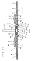
- FIG. 1 is an enlarged cross-sectional view showing a part of the structure of an electronic device according to the present invention.
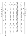
- FIG. 2 is a partly omitted plan view of the electronic device.
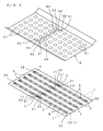
- FIG. 3 is a partly exploded schematic perspective view of the electronic device.
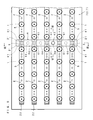
- FIG. 4 is a plan view showing a condition where a reflecting sheet is eliminated.
- FIG. 5 is a plan view showing a condition where the reflecting sheet is absent and a board holder is attached.
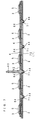
- FIG. 6 is an enlarged cross-sectional view taken along the line VI-VI of FIG. 5 in a condition where the reflecting sheet is present.
- FIG. 7 is an enlarged cross-sectional view taken along the line VII-VII of FIG. 5 in a condition where the reflecting sheet is present.
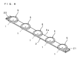
- FIG. 8 is a perspective view showing the structure of a light emitting diode board to which lenses are attached.
- the shown electronic device is attached to the back side of a display section of a flat display apparatus having the display section that has a display screen on the front side and has a substantially rectangular parallelepiped shape.
- the electronic device has: a plurality of light emitting diodes 1 as light sources disposed in parallel in a grid pattern; a plurality of light emitting diode boards 2 disposed in parallel in a lattice pattern and having the light emitting diodes 1 mounted on one surfaces 2a; a plurality of connectors 3 connecting the adjacent light emitting diode boards 2, 2; a board holder 4 that holds the light emitting diode boards 2; a plurality of lenses 5 attached to the one surfaces 2a of the light emitting diode boards 2 so as to face the top portions of the light emitting diodes 1 and diverging the light emitted by the light emitting diodes 1; a reflecting sheet 6 having through holes 61 in which the lenses 5 are disposed and facing the one surfaces 2a to reflect the light diverged by the lenses 5;
- the light emitting diode boards 2 each have a strip shape having a circuit section on the one surface 2a, and are disposed in parallel in a plurality of rows so as to be separated from each other in the longitudinal direction and in the width direction on one surface 7a of the support member 7 having a substantially rectangular shape.
- a plurality of light emitting diodes 1 are mounted so as to be separated in the longitudinal direction.
- connecting sections 21, 22 each having a terminal are provided on both end portions in the longitudinal direction of the one surface 2a. In a position biased toward the other end side from the connecting section 21 on one end portion in the longitudinal direction, a hole 23 penetrating in the thickness direction is provided.
- the two adjacent connecting sections 21, 21 of the light emitting diode boards 2 in each row are connected together by the connector 3, the connecting section 22 of one light emitting diode board 2 is connected to a later-described power supply circuit board by a second connector, and the connecting section 22 of the other light emitting diode board 2 is connected to a later-described control circuit board by a third connector.
- the connector 3 has a substantially rectangular parallelepiped shape. On both end portions in the longitudinal direction of one surface of the connector 3, terminals corresponding to the connecting sections 21, 21 are provided, and when terminals are connected to the connecting portions 21, 21, the connector 3 polymerize on the one surfaces 2a of the light emitting diode boards 2.
- the board holder 4 has: a plurality of protruding sections 41, 41 to be inserted in the holes 23, 23 formed in one end portions of the light emitting diode boards 2 in each row in the light emitting diode boards 2 disposed in parallel in a plurality of rows in such a way that one end portions in the longitudinal direction face each other; a strip-shaped coupling section 42 that couples base ends of the protruding sections 41, 41; a columnar section 43 protruding from the coupling section 42 in a direction opposite to the protruding sections 41, 41 and an end of which is in contact with a sheet surface of a later-described optical sheet to thereby limit a bend of the optical sheet; and an attachment sections 44 protruding from the coupling section 42 in the same direction as the protruding sections 41, 41 and inserted to be latched in attachment holes 71 formed in the support member 7.
- the board holder 4 is structured so that the protruding sections 41, 41 are inserted in the holes 23 to thereby hold the
- protruding sections 41, 41 two that are separated in the longitudinal direction of the light emitting diode boards 2 and the peripheral surfaces of which face each other are disposed in parallel in a plurality of rows in accordance with the separation distance in the row direction of the light emitting diode boards 2.
- the protruding sections 41, 41 are formed, integrally with the coupling section 42, of polycarbonate that is excellent in light reflectivity.
- substantially conical insertion sections 41a are provided on the end portions of the protruding sections 41, 41.
- the coupling section 42 is structured so as to face the other surfaces of a plurality of connectors 3 connecting the adjacent light emitting diode boards 2 in a plurality of rows.
- the columnar section 43 has a substantially conical shape, and is formed integrally with the coupling section 42.
- the attachment sections 44 each have: a plate-like protrusion 44a protruding in the same direction as the protruding sections 41 from between the protruding sections 41 separated in the longitudinal direction of the coupling section 42; and two claws 44b strung out at the end of the plate-like protrusion 44a and latched to the hole edge portion of the attachment hole 71.
- the light emitting diodes 1 are mounted, as shown in FIG. 8 , for example, five or six in number in such a way as to be separated in the longitudinal direction of the light emitting diode board 2, and in accordance with the light emitting diodes 1, five or six lenses 5 are attached to the one surface 2a by an adhesive agent.
- the lens 5 has: a light permeable section 51 that faces the top portion of the light emitting diode 1 so as to be separated therefrom, and has a hemispherical concave portion for diverging in every direction the light emitted by the light emitting diode 1; and three positioning protrusions 52 that protrude from the surface of the light permeable section 51 facing the one surface 2a toward the light emitting diode board 2 and position the light permeable section 51 with respect to the light emitting diode board 2.
- the ends of the positioning protrusions 52 are attached to the one surface 2a by an adhesive agent.
- the positioning protrusions 52 are formed such that the distance between the light permeable section 51 and the light emitting diode boards 2 is slightly longer than the thickness of the reflecting sheet 6 so that the thermal expansion of the reflecting sheet 6 can be absorbed.
- the reflecting sheet 6 is formed of one synthetic resin sheet having high reflectivity and being substantially rectangular in accordance with the support member 7, has second holes 62 formed in positions corresponding to the holes 23 of the light emitting diode boards 2, has through holes 61 formed in positions corresponding to the lenses 5, has second through holes 63 formed in positions corresponding to the connectors 3, and has insertion holes 64 formed in positions corresponding to the attachment sections 44.
- the through holes 61 have a round shape having a slightly larger diameter than the light permeable sections 51, and are arranged in a grid pattern.
- the light permeable sections 51 are disposed thereinside.
- the second through holes 63 are substantially rectangular, and the connectors 3 are inserted therein.
- the insertion holes 64 have a round shape formed between the second through holes 63, and the attachment sections 44 are inserted therein.
- the support member 7 is formed by shaping a metal plate, and has a plate section 72 having a substantially rectangular flat plate form and a frame section 73 ranging along the edge of the plate section 72.
- a plate section 72 In the plate section 72, holes 74 in which the protruding sections 41, 41 of the board holder 4 are inserted and a plurality of attachment holes 71 for attaching the board holder 4 inside the support member 7 are formed.
- the light emitting diode boards 2 are accommodated and supported in such a way as to be arranged in the longitudinal direction and in the width direction.
- a power supply circuit board is attached that is connected to drivers of the light emitting diode boards 2 by the second connectors and supplies a voltage to the drivers
- a control circuit board is attached that is connected to the drivers of the light emitting diode boards 2 by the third connectors and controls the drivers.
- a plurality of circuit boards are attached such as a power supply circuit board that supplies a voltage to the display section, a terminal circuit board that processes the image to be displayed on the display screen of the display section and a control circuit board that controls the display section.
- the support member 7 is placed on a workbench so that its opened side faces upward; on the one surface 7a of the plate section 72 of the support member 7, the two light emitting diode boards 2, 2 adjacent to each other in the row direction are disposed in parallel in a plurality of rows; to the connecting sections 21, 21 provided on adjacent one end portions of the light emitting diode boards 2, 2 in each row, the connectors 3 are connected; and on one surfaces of the light emitting diode boards 2 in each row, the reflecting sheet 6 is placed so as to face them.
- the light permeable sections 51 of the lenses 5 are inserted in the through holes 61 of the reflecting sheet 6, and the connectors 3 are inserted in the second through holes 63.
- the protruding sections 41, 41 of the board holder 4 are inserted into the holes 23 of the light emitting diode boards 2 from the second holes 62 of the reflecting sheet 6, further, the insertion sections 41a at the end of the protruding sections 41, 41 are inserted into the holes 74 of the support member 7, a plurality of light emitting diode boards 2 can be simultaneously held on the support member 7, and the reflecting sheet 6 can be pressed against the one surfaces 2a of the light emitting diode boards 2.
- the attachment sections 44 of the board holder 4 are inserted in the attachment holes 71 of the support member 7 from the insertion holes 64 to be latched, the light emitting diode boards 2 and the reflecting sheet 6 can be secured to the support member 7 by the board holder 4, and the reflecting sheet 6 can be prevented from rising from the light emitting diode boards 2.
- FIG. 9 is a cross-sectional view showing the structure of a display apparatus having the electronic device according to the present invention.
- This display apparatus has: a display section 80 having on the front side a display screen displaying a television image; an electronic device A disposed on the back side of the display section 80; and a cabinet 81 that covers the peripheral part of the display section 80 and the back side of the electronic device A.
- the display section 80 has a display panel 82 having the display screen and an optical sheet 83 disposed on the back side of the display panel 82.
- the peripheral part of the display panel 82 is held by being sandwiched between a front holder frame 84 and a back holder frame 85 to form a panel module, and the back holder frame 85 is attached to the peripheral part of the support member 7.
- the optical sheet 83 is a lamination of a comparatively thick diffuser panel that diffuses the light emitted from the light emitting diodes 1 as light sources and a comparatively thin synthetic resin sheet such as a reflective polarization plate, a prism sheet or a diffusing sheet.
- the support member 7 has the plate section 72 and the frame section 73 ranging along the edge of the plate section 72, and the peripheral part of the diffuser plate is supported by the frame section 73.
- the board holder 4 attached to the inside of the support member 7 faces in a position facing a central side portion of the optical sheet 83, at a slight distance of an extent that the end of the columnar section 43 is in contact with one surface of the optical sheet 83, and a bend of the optical sheet 83 is limited to keep the distance between the optical sheet 83 and the light emitting diodes 1 uniform.
- the cabinet 81 has a cabinet front member 81a that covers the front side of the peripheral part of the display section 80 and a bowl-like cabinet back member 81b that covers the peripheral part of the electronic device A and the back side, and is attached to the frame section 73 of the support member 7 by male screws.
- This electronic device is structured so that, as shown in FIGS. 6 and 7 , the connecting section 42 of the board holder 4 covers the connectors 3.
- the board holder 4 is formed of a synthetic resin such as polycarbonate that is excellent in light reflectivity.
- the coupling section 42 is formed in a length corresponding to the distance between the light emitting diode boards 2 in the outermost two rows and in a width wider than the connectors 3, faces the other surfaces of a plurality of connectors 3 connecting the adjacent light emitting diode boards 2 in a plurality of rows, and covers the connectors 3.
- the connectors 3 normally are not white enough to have high reflectivity, if the connectors 3 are exposed, this causes brightness nonuniformity; however, in this electronic device, a plurality of connectors 3 connecting the adjacent light emitting diode boards 2 in a plurality of rows can be covered with the coupling section 42 that is excellent in light reflectivity, and brightness nonuniformity can be reduced. Since other structures and workings are similar to those of the first embodiment, like parts are denoted by like reference numerals, and detailed descriptions thereof and descriptions of workings and effects are omitted.
- FIG. 10 is an enlarged cross-sectional view showing another structure of the relevant part of the electronic device.
- This electronic device is structured so that connectors 45 connected to the connecting sections 21, 21 of the adjacent light emitting diode boards 2, 2 are provided between the protruding sections 41, 41 of the coupling section 42 of the board holder 4 such that the connecting sections 21, 21 of the adjacent light emitting diode boards 2, 2 can be connected by the board holder 4.
- the connectors 45 is formed of a conductive plate having: a fixed section 45a fixed to the coupling section 42 by fixing means such as an adhesive agent, coupling of concave and convex portions or riveting; and curved connecting sections 45b, 45b ranging on both ends of the fixed section 45a.
- the connectors 45 is structured so that when the protruding sections 41, 41 are inserted in the holes 23, 23, the connecting sections 45b, 45b are connected to the connecting sections 21, 21 of the light emitting diode boards 2, 2.
- FIG. 11 is an enlarged plan view showing another structure of the relevant part of the electronic device.
- the distances H between the adjacent rows of the light emitting diode boards 2 disposed in a plurality of rows are varied, in other words, the parallel disposition pitches between the rows of the light emitting diode boards 2 are varied.
- the intra-row distances on the central side are short, whereas the intra-row distances on both end sides are long.
- the board holder 4 and the reflecting sheet 6 are formed in accordance with the distances H between the rows of the light emitting diode boards 2. Since other structures and workings are similar to those of the first embodiment, like parts are denoted by like reference numerals, and detailed descriptions thereof and descriptions of workings and effects are omitted.
- FIG. 12 is a plan view showing another structure of the relevant part of the electronic device.
- the numbers of light emitting diodes 1 mounted on the light emitting diode boards 2 disposed in parallel in the row direction are varied among positions in the row direction.
- FIG. 12 four light emitting diode boards 2 are disposed in parallel in the row direction, the numbers of light emitting diodes 1 on one side and on the other side in the row direction are five, and the numbers of light emitting diodes 1 on the central side in the row direction are six.
- the through holes 61 are formed in the reflecting sheet 6 in accordance with the number of mounted light emitting diodes 1.
- the light emitting diode boards 2 having different numbers of light emitting diodes 1 can be combined in accordance with the size of the display screen of the display apparatus, the basic shapes of the light emitting diode boards 2, the board holder 4 and the reflecting sheet 6 can be made the same, the assembly workability, and the productivity of parts such as the board holder 4 can be improved, and cost can be further reduced. Since other structures and workings are similar to those of the first embodiment, like parts are denoted by like reference numerals, and detailed descriptions thereof and descriptions of workings and effects are omitted.
- FIG. 13 is a schematic view showing another relationship between the light emitting diode boards 2 and the board holder 4.
- the light emitting diode boards 2 disposed in parallel in the row direction are arranged in a plurality of rows, and four adjacent light emitting diode boards 2 are held on the support member 7 by one board holder 4.
- the light emitting diode boards 2 each have a rectangular shape where the light emitting diodes 1 are mounted so as to be separated in the longitudinal direction and in the width direction.
- the hole 23 is provided in one angular part of each of the light emitting diode boards 2, and a plurality of holes 74 corresponding to the holes 23 are provided in the support member 7.
- the two adjacent light emitting diode boards 2, 2 in one row and the two light emitting diode boards 2, 2 in the adjacent row can be simultaneously held on the support member 7, and the assembly workability can be further improved. Since other structures and workings are similar to those of the first to fifth embodiments, like parts are denoted by like reference numerals, and detailed descriptions thereof and descriptions of workings and effects are omitted.
- FIG. 14 is a schematic view showing another relationship between the light emitting diode boards 2 and the board holder 4.
- the light emitting diode boards 2 disposed in parallel in the row direction are arranged on the support member 7 in a plurality of rows so as to be alternately biased in a direction orthogonally intersecting the row direction into a staggered pattern, and the adjacent light emitting diode boards 2 in a plurality of rows are held on the support member 7 by the board holder 4.
- the light emitting diode boards 2 have a strip shape, the holes 23 are provided at one end portions in the longitudinal direction, and a plurality of holes 74 corresponding to the holes 23 are disposed on the support member 7 in a staggered pattern.
- the board holder 4 has a strip shape of a length corresponding to the distance between the two light emitting diode boards 2 in the outermost rows, and a plurality of protruding sections 41 corresponding to the light emitting diode boards 2 adjacent in the row direction are arranged in a staggered pattern so as to be separated in the width direction.
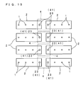
- FIG. 15 is a schematic view showing another relationship between the light emitting diode boards 2 and the board holder 4.
- the light emitting diode boards 2 disposed in parallel in the row direction are arranged in a plurality of rows on the support member 7, and the light emitting diode boards 2, 2 adjacent in positions in the row direction are held on the support member 7 by the board holder 4.
- the light emitting diode boards 2 are formed in a strip shape, the holes 23 are provided at one end portions in the longitudinal direction, and a plurality of holes 74 corresponding to the holes 23 are provided in the support member 7.
- two protruding sections 41, 41 are disposed in parallel so as to be separated from each other.
- the light emitting diode boards 2, 2 adjacent in positions in the row direction can be simultaneously held on the support member 7, and the assembly workability can be further improved. Since other structures and workings are similar to those of the first to fifth embodiments, like parts are denoted by like reference numerals, and detailed descriptions thereof and descriptions of workings and effects are omitted.
- FIG. 16 is a schematic view showing another relationship between the light emitting diode boards 2 and the board holder 4.
- the light emitting diode boards 2 disposed in parallel in the row direction are arranged on the support member 7 in a plurality of rows so as to be alternately biased in a direction orthogonally intersecting the row direction into a staggered pattern, and the three light emitting diode boards 2, 2, 2 adjacent to one another are held on the support member 7 by one board holder 4.
- the light emitting diode boards 2 are formed in a strip shape, there are first light emitting diode boards 2b each having the hole 23 at one end portion in the longitudinal direction and second light emitting diode boards 2c each having the hole 23 in an angular part at one end portion in the longitudinal direction, the first and second light emitting diodes 2b and 2c are arranged in a staggered pattern, and a plurality of holes 74 corresponding to the holes 23 are arranged in a staggered pattern on the support member 7.
- the board holder 4 is provided with three protruding sections 41 corresponding to the holes 23 of the three adjacent light emitting diode boards 2b, 2c, 2c.
- the three light emitting diode boards 2b, 2c, 2c arranged in a staggered pattern can be simultaneously held on the support member 7, and the assembly workability can be further improved. Since other structures and workings are similar to those of the first to fifth embodiments, like parts are denoted by like reference numerals, and detailed descriptions thereof and descriptions of workings and effects are omitted.
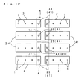
- FIG. 17 is a schematic view showing another relationship between the light emitting diode boards 2 and the board holder 4.
- the light emitting diode boards 2 disposed in parallel in the row direction are arranged in a plurality of rows, and the two adjacent light emitting diode boards 2, 2 in one row and the two light emitting diode boards 2, 2 in the adjacent row are simultaneously held on the support member 7 by one board holder 4.
- the light emitting diode boards 2 are formed in a strip shape, the holes 23 are provided at one end portions in the longitudinal direction, and a plurality of holes 74 corresponding to the holes 23 are provided in the support member 7.
- the two protruding sections 41 facing so as to be separated are provided in two rows.
- the two adjacent light emitting diode boards 2, 2 in one row and the two light emitting diode boards 2, 2 in the adjacent row can be simultaneously held on the support member 7, and the assembly workability can be further improved. Since other structures and workings are similar to those of the first to fifth embodiments, like parts are denoted by like reference numerals, and detailed descriptions thereof and descriptions of workings and effects are omitted.
- FIG. 18 is a cross-sectional view showing another structure of the relevant part of the electronic device according to the present invention.
- the columnar section 43 of the board holder 4 is eliminated.
- a sheet receiver that is in contact with the sheet surface of the optical sheet 83 to thereby limit a bend of the optical sheet 83 is separately provided as required, and attachment holes for attaching the sheet receiver are provided in the support member 7 or the light emitting diode boards 2. Since other structures and workings are similar to those of the first to fifth embodiments, like parts are denoted by like reference numerals, and detailed descriptions thereof and descriptions of workings and effects are omitted.
- the light emitting diode boards 2 having the same length are disposed in parallel so as to be separated in the width direction and the parts where the light emitting diode boards 2 in each row adjoin each other are aligned in the width direction of the light emitting diode boards 2, additionally, a structure may be adopted such that the light emitting diode boards 2 having different lengths are disposed in parallel so as to be separated in the width direction and the parts where the light emitting diode boards 2 adjoin each other in each row are varied, for example, in a staggered pattern or linearly biased in a direction intersecting the longitudinal direction of the light emitting diode boards 2, and the structure of combination of the light emitting diode boards 2 is not specifically limited.
- the board holder 4 and the reflecting sheet 6 are formed in accordance with the structure of combination of the light emitting diode boards 2.
- the board holder 4 presses the reflecting sheet 6 toward the light emitting diode boards 2, additionally, the board holder 4 may hold the light emitting diode boards 2 without pressing the reflecting sheet 6.
Landscapes
- Physics & Mathematics (AREA)
- Nonlinear Science (AREA)
- Mathematical Physics (AREA)
- Chemical & Material Sciences (AREA)
- Crystallography & Structural Chemistry (AREA)
- General Physics & Mathematics (AREA)
- Optics & Photonics (AREA)
- Microelectronics & Electronic Packaging (AREA)
- Engineering & Computer Science (AREA)
- Planar Illumination Modules (AREA)
- Led Device Packages (AREA)
- Fastening Of Light Sources Or Lamp Holders (AREA)
- Liquid Crystal (AREA)
- Non-Portable Lighting Devices Or Systems Thereof (AREA)
- Combinations Of Printed Boards (AREA)
- Devices For Indicating Variable Information By Combining Individual Elements (AREA)
Abstract
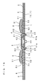
Provided are a board holder which can easily hold the relative positions of a plurality of circuit boards disposed in parallel without using a screw, an electronic device which can easily affix the circuit boards held by the board holder, and a display apparatus including the electronic device. A hole (23) that penetrates each light emitting diode board (2) in the thickness direction of the board is provided, on one end portion in the longitudinal direction of each of a plurality of light emitting diode boards (2) which have a plurality of light emitting diodes (1) mounted on one surface, respectively have substantially a strip shape, and are arranged in a plurality of rows. The board holder (4) has: protruding sections (41, 41) which are inserted into the holes (23, 23) of the adjacent light emitting diode boards (2, 2); and a coupling section (42) which is disposed in the direction orthogonally intersecting the longitudinal direction of the light emitting diode board (2), has a strip-shape, and couples respective base ends of the protruding sections (41, 41). The plurality of light emitting diode boards (2) disposed in parallel are held by inserting the protruding sections (41, 41) into the holes (23, 23).
Description
- The present invention relates to a board holder that holds a plurality of circuit boards disposed in parallel, an electronic device having the board holder, and a display apparatus having the electronic device.
- In a display apparatus such as a television, on the back side of a display section having a display screen displaying an image on the front side, an electronic device is disposed that has a light source for irradiating the display section.
- The electronic device is provided with, for example, a plurality of light emitting diode boards disposed in parallel and having a plurality of light emitting diodes mounted on one surface, a plurality of lenses that diverge the light emitted by the light emitting diodes, a lens cover that has through holes in which the lenses are disposed and sandwiches peripheral parts of the lenses with the light emitting diode boards, and a backlight frame that supports the light emitting diode boards disposed in parallel (see, for example, Patent Document 1).
- A plurality of insertion holes are formed in the light emitting diode boards and the lens cover, attachment holes corresponding to the insertion holes are formed in the backlight frame, and male screws inserted in the insertion holes of the light emitting diode boards and the lens cover are screwed into the attachment holes, whereby the light emitting diode boards and the lens cover are fixed to the backlight frame and the peripheral parts of the lenses are sandwiched between peripheral parts of the through holes in the lens cover and the light emitting diode boards to thereby fix the lenses.
-
- Patent Document 1: Japanese Patent Application Laid-Open No.
2008-41546 - However, in the electronic device structured so that a plurality of light emitting diode boards disposed in parallel are individually fixed by male screws as in
Patent Document 1, there is a problem in that the number of man-hours for screwing the male screws increases, the workability of attachment of the light emitting diode boards is poor and this results in high cost. - The present invention has been made with the aim of solving the above problems, and it is an object of the present invention to provide: a board holder capable of easily holding a plurality of circuit boards disposed in parallel, on a support member, without using a screw; an electronic device having the board holder; and a display apparatus having the electronic device.
- A board holder according to the present invention is a board holder that holds, on a support member for supporting a plurality of circuit boards disposed in parallel, the circuit boards, and is characterized by comprising: a plurality of protruding sections to be inserted in holes formed in an adjacent circuit boards and the support member; and a coupling section coupling the protruding sections.
- in this invention, by inserting the protruding sections of the board holder from the holes of the adjacent circuit boards into the holes of the support member in a condition where a plurality of circuit boards having the holes corresponding to the holes of the support member are disposed in parallel on the support member having the holes, the adjacent circuit boards can be simultaneously held on the support member, the separation distances between the circuit boards can be made uniform, and the circuit boards can be secured in this condition, so that the workability of attachment of the circuit boards disposed in parallel onto the support member can be improved.
- Moreover, preferably, the protruding sections of the board holder according to the present invention are arranged in a plurality of rows.
In this invention, when a plurality of circuit boards having the holes are arranged in a plurality of rows, by inserting the protruding sections of one board holder into the holes of a plurality of circuit boards, the circuit boards in a plurality of rows can be simultaneously held on the support member, the separation distances between the circuit boards in a plurality of rows can be made uniform, and the circuit boards can be secured in this condition, so that the workability of attachment of the circuit boards disposed in parallel onto the support member can be improved. - Moreover, preferably, the coupling section of the board holder according to the present invention has an attachment section attached to the support member.
In this invention, when the protruding sections of one board holder are inserted in the holes of a plurality of circuit boards, the attachment section of the board holder can be attached to the support member, so that the circuit boards can be firmly secured without any increase in the number of parts. - Moreover, preferably, the coupling section of the board holder according to the present invention has a columnar section having an end contacting with a sheet surface of an optical sheet disposed facing to the circuit boards with a space therebetween, thereby limiting a bend of the optical sheet.
In this invention, a bend, toward the circuit board side, of the optical sheet disposed facing to the circuit boards with a space therebetween can be restrained by the columnar section without any increase in the number of parts, so that the optical characteristic by the optical sheet can be stabilized. - Moreover, preferably, the board holder according to the present invention has a connector between the protruding sections of the coupling section.
In this invention, when the protruding sections of the board holder are inserted in the holes of the adjacent circuit boards to thereby hold the circuit boards on the support member, the connector of the coupling section can be connected to the connecting sections of the adjacent circuit boards, in other words, the board holder itself constitutes the connector, so that the workability of connection of the circuit boards by the connector can be improved. Moreover, the connector can be covered with the coupling section, so that the brightness characteristic can be improved. - Moreover, an electronic device according to the present invention is characterized by comprising: a plurality of circuit boards disposed in parallel and having a light emitting diode mounted thereon; and the above-described board holder.
In this invention, by inserting the protruding sections of the board holder into the holes of the adjacent circuit boards in a condition where a plurality of circuit boards having the holes are disposed in parallel, the adjacent circuit boards can be held on the support member, the separation distances between the circuit boards can be made uniform, and the circuit boards can be secured to the support member in this condition, so that the workability of attachment of the circuit boards disposed in parallel can be improved. - Moreover, preferably, in the electronic device according to the present invention, the circuit boards are arranged in a plurality of rows.
In this invention, by inserting the protruding sections of one board holder into the holes of a plurality of circuit boards, the circuit boards in a plurality of rows can be held on the support member, the separation distances between the circuit boards in a plurality of rows can be made uniform, and the circuit boards can be attached to the support member in this condition, so that the workability of attachment of the circuit boards disposed in parallel can be improved. - Moreover, preferably, in the electronic device according to the present invention, on one surface of each of the circuit boards, a circuit section and the light emitting diode are disposed, and a connecting section for connecting the adjacent circuit boards together by the connector is provided on the one surface.
In this invention, the circuit boards each having the circuit section on one surface can be disposed in parallel in such a way that the other surfaces are two-dimensionally aligned, so that the thickness of the circuit board portion can be reduced and the electronic device can be reduced in thickness. Moreover, the other surfaces of the circuit boards disposed in parallel can be brought close to the support member supporting the circuit boards without affected by the connectors, so that it is unnecessary to form through holes corresponding to the connectors in the support member and the dust-proofness of the circuit board portion can be improved. - Moreover, preferably, in the electronic device according to the present invention, the connector is provided on the coupling section.
In this invention, the board holder itself constitutes the connector, so that it is not particularly necessary to operate the connector and the workability of connection of the circuit boards by the connector can be improved. Moreover, the connector can be covered with the coupling section, so that the brightness characteristic can be improved. - Moreover, preferably, in the electronic device according to the present invention, a support member that supports the circuit boards is provided, and the support member and the circuit boards are provided with holes in which the protruding sections are inserted.
In this invention, when the protruding sections of one board holder are inserted in the holes of a plurality of circuit boards, the attachment sections of the board holder can be attached to the support member, so that the circuit boards can be firmly secured without any increase in the number of parts. - Moreover, preferably, the electronic device according to the present invention is provided with a reflecting sheet that has a through hole in which the light emitting diode is disposed and second holes in which the protruding sections are inserted, and faces the circuit boards to reflect light emitted by the light emitting diode.
In this invention, by inserting the protruding sections of the board holder from the second holes of the reflecting sheet into the holes of the circuit boards, a plurality of circuit boards disposed in parallel and the reflecting sheet can be held on the support member, and the light emitting diodes can be disposed in the through holes of the reflecting sheet, so that the workability of assembly of the reflecting sheet can be improved. Moreover, it is not particularly necessary to provide a reflecting sheet holding member, so that the number of parts can be reduced and cost can be reduced. - Moreover, preferably, in the electronic device according to the present invention, adjacent rows of the circuit boards are separated by different distances.
In this invention, the distances between the rows of the circuit boards can be varied in accordance with the number of light emitting diode boards disposed in parallel, so that the brightness characteristic can be set to an optimum one in accordance with the size of the display screen of the display apparatus in which the electronic device is incorporated. - Moreover, preferably, in the electronic device according to the present invention, the numbers of light emitting diodes mounted on the circuit boards disposed in parallel are different.
In this invention, the lengths of a plurality of circuit boards disposed in parallel in the row direction can be varied, so that the light emitting diode boards having different numbers of light emitting diodes can be combined in accordance with the size of the display section of the display apparatus in which the electronic device is incorporated, the basic shapes of the light emitting diode boards and the board holder can be made the same, the assembly workability, and the productivity of parts such as the board holder can be improved, and cost can be further reduced. - Moreover, a display apparatus according to the present invention is characterized by comprising a display section having a display screen on one side and the above-described electronic device disposed on the other side of the display section.
In this invention, by inserting the protruding sections of one board holder into the holes of the circuit boards in a plurality of rows, the circuit boards in a plurality of rows can be simultaneously held on the support member, the separation distances between the circuit boards in a plurality of rows can be made uniform, and the circuit boards can be secured to the support member in this condition, so that the workability of attachment of the circuit boards disposed in parallel can be improved. - According to the present invention, by inserting the protruding sections of the board holder into the holes of the adjacent circuit boards and the holes of the support member in a condition where a plurality of circuit boards having the holes are disposed in parallel, the adjacent circuit boards can be simultaneously held on the support member, and the separation distances between the circuit boards can be made uniform, so that the workability of attachment of the circuit boards disposed in parallel onto the support member can be improved and cost can be reduced.
-
-
FIG. 1 is an enlarged cross-sectional view showing a part of the structure of an electronic device according to the present invention; -
FIG. 2 is a partly omitted plan view of the electronic device according to the present invention; -
FIG. 3 is a partly exploded schematic perspective view of the electronic device according to the present invention; -
FIG. 4 is a plan view showing a condition where a reflecting sheet of the electronic device according to the present invention is eliminated; -
FIG. 5 is a plan view showing a condition where the reflecting sheet of the electronic device according to the present invention is absent and a board holder is attached; -
FIG. 6 is an enlarged cross-sectional view taken along the line VI-VI ofFIG. 5 in a condition where the reflecting sheet is present; -
FIG. 7 is an enlarged cross-sectional view taken along the line VII-VII ofFIG. 5 in a condition where the reflecting sheet is present; -
FIG. 8 is a perspective view showing the structure of a light emitting diode board to which lenses are attached in the electronic device according to the present invention; -
FIG. 9 is a cross-sectional view showing the structure of a display apparatus having the electronic device according to the present invention; -
FIG. 10 is an enlarged cross-sectional view showing another structure of the relevant part of the electronic device according to the present invention; -
FIG. 11 is an enlarged plan view showing another structure of the relevant part of the electronic device according to the present invention; -
FIG. 12 is a plan view showing another structure of the relevant part of the electronic device according to the present invention; -
FIG. 13 is a schematic view showing another relationship between the light emitting diode boards and the board holder of the electronic device according to the present invention; -
FIG. 14 is a schematic view showing another relationship between the light emitting diode boards and the board holder of the electronic device according to the present invention; -
FIG. 15 is a schematic view showing another relationship between the light emitting diode boards and the board holder of the electronic device according to the present invention; -
FIG. 16 is a schematic view showing another relationship between the light emitting diode boards and the board holder of the electronic device according to the present invention; -
FIG. 17 is a schematic view showing another relationship between the light emitting diode boards and the board holder of the electronic device according to the present invention; and -
FIG. 18 is a cross-sectional view showing another structure of the relevant part of the electronic device according to the present invention. - The following will describe in detail the present invention with reference to the drawings illustrating some embodiments thereof.
-
FIG. 1 is an enlarged cross-sectional view showing a part of the structure of an electronic device according to the present invention.FIG. 2 is a partly omitted plan view of the electronic device.FIG. 3 is a partly exploded schematic perspective view of the electronic device.FIG. 4 is a plan view showing a condition where a reflecting sheet is eliminated.FIG. 5 is a plan view showing a condition where the reflecting sheet is absent and a board holder is attached.FIG. 6 is an enlarged cross-sectional view taken along the line VI-VI ofFIG. 5 in a condition where the reflecting sheet is present.FIG. 7 is an enlarged cross-sectional view taken along the line VII-VII ofFIG. 5 in a condition where the reflecting sheet is present.FIG. 8 is a perspective view showing the structure of a light emitting diode board to which lenses are attached. - The shown electronic device is attached to the back side of a display section of a flat display apparatus having the display section that has a display screen on the front side and has a substantially rectangular parallelepiped shape. The electronic device has: a plurality of
light emitting diodes 1 as light sources disposed in parallel in a grid pattern; a plurality of light emittingdiode boards 2 disposed in parallel in a lattice pattern and having thelight emitting diodes 1 mounted on one surfaces 2a; a plurality ofconnectors 3 connecting the adjacent light emittingdiode boards board holder 4 that holds the light emittingdiode boards 2; a plurality oflenses 5 attached to the one surfaces 2a of the light emittingdiode boards 2 so as to face the top portions of thelight emitting diodes 1 and diverging the light emitted by thelight emitting diodes 1; a reflectingsheet 6 having throughholes 61 in which thelenses 5 are disposed and facing the one surfaces 2a to reflect the light diverged by thelenses 5; and asupport member 7 that supports the light emittingdiode boards 2 arranged in a plurality of rows. - The light emitting
diode boards 2 each have a strip shape having a circuit section on the one surface 2a, and are disposed in parallel in a plurality of rows so as to be separated from each other in the longitudinal direction and in the width direction on one surface 7a of thesupport member 7 having a substantially rectangular shape. On the one surface 2a of each of the light emittingdiode boards 2, as shown inFIG. 8 , a plurality oflight emitting diodes 1 are mounted so as to be separated in the longitudinal direction. On both end portions in the longitudinal direction of the one surface 2a, connectingsections section 21 on one end portion in the longitudinal direction, ahole 23 penetrating in the thickness direction is provided. - In the light emitting
diode boards 2 disposed in parallel in a plurality of rows in such a way that one end portions in the longitudinal direction face each other, the two adjacent connectingsections diode boards 2 in each row are connected together by theconnector 3, the connectingsection 22 of one light emittingdiode board 2 is connected to a later-described power supply circuit board by a second connector, and the connectingsection 22 of the other light emittingdiode board 2 is connected to a later-described control circuit board by a third connector. - The
connector 3 has a substantially rectangular parallelepiped shape. On both end portions in the longitudinal direction of one surface of theconnector 3, terminals corresponding to the connectingsections portions connector 3 polymerize on the one surfaces 2a of the light emittingdiode boards 2. - The
board holder 4 has: a plurality of protrudingsections holes diode boards 2 in each row in the light emittingdiode boards 2 disposed in parallel in a plurality of rows in such a way that one end portions in the longitudinal direction face each other; a strip-shapedcoupling section 42 that couples base ends of the protrudingsections columnar section 43 protruding from thecoupling section 42 in a direction opposite to the protrudingsections attachment sections 44 protruding from thecoupling section 42 in the same direction as the protrudingsections support member 7. Theboard holder 4 is structured so that the protrudingsections holes 23 to thereby hold the light emittingdiode boards 2 in relative positions. - As for the protruding
sections diode boards 2 and the peripheral surfaces of which face each other are disposed in parallel in a plurality of rows in accordance with the separation distance in the row direction of the light emittingdiode boards 2. The protrudingsections coupling section 42, of polycarbonate that is excellent in light reflectivity. On the end portions of the protrudingsections - The
coupling section 42 is structured so as to face the other surfaces of a plurality ofconnectors 3 connecting the adjacent light emittingdiode boards 2 in a plurality of rows. - The
columnar section 43 has a substantially conical shape, and is formed integrally with thecoupling section 42. - The
attachment sections 44 each have: a plate-like protrusion 44a protruding in the same direction as the protrudingsections 41 from between the protrudingsections 41 separated in the longitudinal direction of thecoupling section 42; and two claws 44b strung out at the end of the plate-like protrusion 44a and latched to the hole edge portion of theattachment hole 71. - The
light emitting diodes 1 are mounted, as shown inFIG. 8 , for example, five or six in number in such a way as to be separated in the longitudinal direction of the light emittingdiode board 2, and in accordance with thelight emitting diodes 1, five or sixlenses 5 are attached to the one surface 2a by an adhesive agent. - The
lens 5 has: a lightpermeable section 51 that faces the top portion of thelight emitting diode 1 so as to be separated therefrom, and has a hemispherical concave portion for diverging in every direction the light emitted by thelight emitting diode 1; and threepositioning protrusions 52 that protrude from the surface of the lightpermeable section 51 facing the one surface 2a toward the light emittingdiode board 2 and position the lightpermeable section 51 with respect to the light emittingdiode board 2. The ends of thepositioning protrusions 52 are attached to the one surface 2a by an adhesive agent. - The positioning protrusions 52 are formed such that the distance between the light
permeable section 51 and the light emittingdiode boards 2 is slightly longer than the thickness of the reflectingsheet 6 so that the thermal expansion of the reflectingsheet 6 can be absorbed. - The reflecting
sheet 6 is formed of one synthetic resin sheet having high reflectivity and being substantially rectangular in accordance with thesupport member 7, has second holes 62 formed in positions corresponding to theholes 23 of the light emittingdiode boards 2, has throughholes 61 formed in positions corresponding to thelenses 5, has second throughholes 63 formed in positions corresponding to theconnectors 3, and has insertion holes 64 formed in positions corresponding to theattachment sections 44. - The through holes 61 have a round shape having a slightly larger diameter than the light
permeable sections 51, and are arranged in a grid pattern. The lightpermeable sections 51 are disposed thereinside. The second throughholes 63 are substantially rectangular, and theconnectors 3 are inserted therein. The insertion holes 64 have a round shape formed between the second throughholes 63, and theattachment sections 44 are inserted therein. - The
support member 7 is formed by shaping a metal plate, and has aplate section 72 having a substantially rectangular flat plate form and aframe section 73 ranging along the edge of theplate section 72. In theplate section 72, holes 74 in which the protrudingsections board holder 4 are inserted and a plurality of attachment holes 71 for attaching theboard holder 4 inside thesupport member 7 are formed. On the one surface 7a of theplate section 72, the light emittingdiode boards 2 are accommodated and supported in such a way as to be arranged in the longitudinal direction and in the width direction. - To one side portion in the longitudinal direction of the other surface of the
plate section 72, a power supply circuit board is attached that is connected to drivers of the light emittingdiode boards 2 by the second connectors and supplies a voltage to the drivers, and to the other side portion in the longitudinal direction, a control circuit board is attached that is connected to the drivers of the light emittingdiode boards 2 by the third connectors and controls the drivers. To a central portion in the longitudinal direction of the other surface of theplate section 72, a plurality of circuit boards are attached such as a power supply circuit board that supplies a voltage to the display section, a terminal circuit board that processes the image to be displayed on the display screen of the display section and a control circuit board that controls the display section. - In the electronic device structured as described above, the
support member 7 is placed on a workbench so that its opened side faces upward; on the one surface 7a of theplate section 72 of thesupport member 7, the two light emittingdiode boards sections diode boards connectors 3 are connected; and on one surfaces of the light emittingdiode boards 2 in each row, the reflectingsheet 6 is placed so as to face them. - In this case, the light
permeable sections 51 of thelenses 5 are inserted in the throughholes 61 of the reflectingsheet 6, and theconnectors 3 are inserted in the second through holes 63. - After the reflecting
sheet 6 is incorporated, the protrudingsections board holder 4 are inserted into theholes 23 of the light emittingdiode boards 2 from thesecond holes 62 of the reflectingsheet 6, further, the insertion sections 41a at the end of the protrudingsections holes 74 of thesupport member 7, a plurality of light emittingdiode boards 2 can be simultaneously held on thesupport member 7, and the reflectingsheet 6 can be pressed against the one surfaces 2a of the light emittingdiode boards 2. Moreover, theattachment sections 44 of theboard holder 4 are inserted in the attachment holes 71 of thesupport member 7 from the insertion holes 64 to be latched, the light emittingdiode boards 2 and the reflectingsheet 6 can be secured to thesupport member 7 by theboard holder 4, and the reflectingsheet 6 can be prevented from rising from the light emittingdiode boards 2. -
FIG. 9 is a cross-sectional view showing the structure of a display apparatus having the electronic device according to the present invention. This display apparatus has: adisplay section 80 having on the front side a display screen displaying a television image; an electronic device A disposed on the back side of thedisplay section 80; and acabinet 81 that covers the peripheral part of thedisplay section 80 and the back side of the electronic device A. - The
display section 80 has adisplay panel 82 having the display screen and anoptical sheet 83 disposed on the back side of thedisplay panel 82. The peripheral part of thedisplay panel 82 is held by being sandwiched between afront holder frame 84 and aback holder frame 85 to form a panel module, and theback holder frame 85 is attached to the peripheral part of thesupport member 7. - The
optical sheet 83 is a lamination of a comparatively thick diffuser panel that diffuses the light emitted from thelight emitting diodes 1 as light sources and a comparatively thin synthetic resin sheet such as a reflective polarization plate, a prism sheet or a diffusing sheet. - The
support member 7 has theplate section 72 and theframe section 73 ranging along the edge of theplate section 72, and the peripheral part of the diffuser plate is supported by theframe section 73. - The
board holder 4 attached to the inside of thesupport member 7 faces in a position facing a central side portion of theoptical sheet 83, at a slight distance of an extent that the end of thecolumnar section 43 is in contact with one surface of theoptical sheet 83, and a bend of theoptical sheet 83 is limited to keep the distance between theoptical sheet 83 and thelight emitting diodes 1 uniform. - The
cabinet 81 has a cabinet front member 81a that covers the front side of the peripheral part of thedisplay section 80 and a bowl-like cabinet back member 81b that covers the peripheral part of the electronic device A and the back side, and is attached to theframe section 73 of thesupport member 7 by male screws. - This electronic device is structured so that, as shown in
FIGS. 6 and7 , the connectingsection 42 of theboard holder 4 covers theconnectors 3. - The
board holder 4 is formed of a synthetic resin such as polycarbonate that is excellent in light reflectivity. - The
coupling section 42 is formed in a length corresponding to the distance between the light emittingdiode boards 2 in the outermost two rows and in a width wider than theconnectors 3, faces the other surfaces of a plurality ofconnectors 3 connecting the adjacent light emittingdiode boards 2 in a plurality of rows, and covers theconnectors 3. - Since the
connectors 3 normally are not white enough to have high reflectivity, if theconnectors 3 are exposed, this causes brightness nonuniformity; however, in this electronic device, a plurality ofconnectors 3 connecting the adjacent light emittingdiode boards 2 in a plurality of rows can be covered with thecoupling section 42 that is excellent in light reflectivity, and brightness nonuniformity can be reduced.
Since other structures and workings are similar to those of the first embodiment, like parts are denoted by like reference numerals, and detailed descriptions thereof and descriptions of workings and effects are omitted. -
FIG. 10 is an enlarged cross-sectional view showing another structure of the relevant part of the electronic device. This electronic device is structured so thatconnectors 45 connected to the connectingsections diode boards sections coupling section 42 of theboard holder 4 such that the connectingsections diode boards board holder 4. - The
connectors 45 is formed of a conductive plate having: a fixed section 45a fixed to thecoupling section 42 by fixing means such as an adhesive agent, coupling of concave and convex portions or riveting; and curved connectingsections connectors 45 is structured so that when the protrudingsections holes sections sections diode boards - In this electronic device, it is not particularly necessary to operate the
connectors 45, and the connectingsections diode boards diode boards 2 by theboard holder 4. Consequently, theconnectors 3 can be covered with thecoupling section 42 constituting theboard holder 4.
Since other structures and workings are similar to those of the first embodiment, like parts are denoted by like reference numerals, and detailed descriptions thereof and descriptions of workings and effects are omitted. -
FIG. 11 is an enlarged plan view showing another structure of the relevant part of the electronic device. In this electronic device, the distances H between the adjacent rows of the light emittingdiode boards 2 disposed in a plurality of rows are varied, in other words, the parallel disposition pitches between the rows of the light emittingdiode boards 2 are varied. - In
FIG. 11 , the intra-row distances on the central side are short, whereas the intra-row distances on both end sides are long. In this case, theboard holder 4 and the reflectingsheet 6 are formed in accordance with the distances H between the rows of the light emittingdiode boards 2.
Since other structures and workings are similar to those of the first embodiment, like parts are denoted by like reference numerals, and detailed descriptions thereof and descriptions of workings and effects are omitted. -
FIG. 12 is a plan view showing another structure of the relevant part of the electronic device. In this electronic device, the numbers oflight emitting diodes 1 mounted on the light emittingdiode boards 2 disposed in parallel in the row direction are varied among positions in the row direction. - In
FIG. 12 , four light emittingdiode boards 2 are disposed in parallel in the row direction, the numbers oflight emitting diodes 1 on one side and on the other side in the row direction are five, and the numbers oflight emitting diodes 1 on the central side in the row direction are six. In this case, the throughholes 61 are formed in the reflectingsheet 6 in accordance with the number of mountedlight emitting diodes 1. - In this electronic device, the light emitting
diode boards 2 having different numbers oflight emitting diodes 1 can be combined in accordance with the size of the display screen of the display apparatus, the basic shapes of the light emittingdiode boards 2, theboard holder 4 and the reflectingsheet 6 can be made the same, the assembly workability, and the productivity of parts such as theboard holder 4 can be improved, and cost can be further reduced.
Since other structures and workings are similar to those of the first embodiment, like parts are denoted by like reference numerals, and detailed descriptions thereof and descriptions of workings and effects are omitted. -
FIG. 13 is a schematic view showing another relationship between the light emittingdiode boards 2 and theboard holder 4. In this electronic device, the light emittingdiode boards 2 disposed in parallel in the row direction are arranged in a plurality of rows, and four adjacent light emittingdiode boards 2 are held on thesupport member 7 by oneboard holder 4. - The light emitting
diode boards 2 each have a rectangular shape where thelight emitting diodes 1 are mounted so as to be separated in the longitudinal direction and in the width direction. Thehole 23 is provided in one angular part of each of the light emittingdiode boards 2, and a plurality ofholes 74 corresponding to theholes 23 are provided in thesupport member 7. - On the
board holder 4, two protrudingsections 41 facing so as to be separated are provided in two rows. - In this electronic device, the two adjacent light emitting
diode boards diode boards support member 7, and the assembly workability can be further improved.
Since other structures and workings are similar to those of the first to fifth embodiments, like parts are denoted by like reference numerals, and detailed descriptions thereof and descriptions of workings and effects are omitted. -
FIG. 14 is a schematic view showing another relationship between the light emittingdiode boards 2 and theboard holder 4. In this electronic device, the light emittingdiode boards 2 disposed in parallel in the row direction are arranged on thesupport member 7 in a plurality of rows so as to be alternately biased in a direction orthogonally intersecting the row direction into a staggered pattern, and the adjacent light emittingdiode boards 2 in a plurality of rows are held on thesupport member 7 by theboard holder 4. - The light emitting
diode boards 2 have a strip shape, theholes 23 are provided at one end portions in the longitudinal direction, and a plurality ofholes 74 corresponding to theholes 23 are disposed on thesupport member 7 in a staggered pattern. - The
board holder 4 has a strip shape of a length corresponding to the distance between the two light emittingdiode boards 2 in the outermost rows, and a plurality of protrudingsections 41 corresponding to the light emittingdiode boards 2 adjacent in the row direction are arranged in a staggered pattern so as to be separated in the width direction. - With this electronic device, a plurality of light emitting
diode boards 2 disposed in a staggered pattern can be simultaneously held on thesupport member 7, and the assembly workability can be further improved.
Since other structures and workings are similar to those of the first to fifth embodiments, like parts are denoted by like reference numerals, and detailed descriptions thereof and descriptions of workings and effects are omitted. -
FIG. 15 is a schematic view showing another relationship between the light emittingdiode boards 2 and theboard holder 4. In this electronic device, the light emittingdiode boards 2 disposed in parallel in the row direction are arranged in a plurality of rows on thesupport member 7, and the light emittingdiode boards support member 7 by theboard holder 4. - The light emitting
diode boards 2 are formed in a strip shape, theholes 23 are provided at one end portions in the longitudinal direction, and a plurality ofholes 74 corresponding to theholes 23 are provided in thesupport member 7. - On the
board holder 4, two protrudingsections - In this electronic device, the light emitting
diode boards support member 7, and the assembly workability can be further improved.
Since other structures and workings are similar to those of the first to fifth embodiments, like parts are denoted by like reference numerals, and detailed descriptions thereof and descriptions of workings and effects are omitted. -
FIG. 16 is a schematic view showing another relationship between the light emittingdiode boards 2 and theboard holder 4. In this electronic device, the light emittingdiode boards 2 disposed in parallel in the row direction are arranged on thesupport member 7 in a plurality of rows so as to be alternately biased in a direction orthogonally intersecting the row direction into a staggered pattern, and the three light emittingdiode boards support member 7 by oneboard holder 4. - The light emitting
diode boards 2 are formed in a strip shape, there are first light emitting diode boards 2b each having thehole 23 at one end portion in the longitudinal direction and second light emitting diode boards 2c each having thehole 23 in an angular part at one end portion in the longitudinal direction, the first and second light emitting diodes 2b and 2c are arranged in a staggered pattern, and a plurality ofholes 74 corresponding to theholes 23 are arranged in a staggered pattern on thesupport member 7. - The
board holder 4 is provided with three protrudingsections 41 corresponding to theholes 23 of the three adjacent light emitting diode boards 2b, 2c, 2c. - In this electronic device, the three light emitting diode boards 2b, 2c, 2c arranged in a staggered pattern can be simultaneously held on the
support member 7, and the assembly workability can be further improved.
Since other structures and workings are similar to those of the first to fifth embodiments, like parts are denoted by like reference numerals, and detailed descriptions thereof and descriptions of workings and effects are omitted. -
FIG. 17 is a schematic view showing another relationship between the light emittingdiode boards 2 and theboard holder 4. In this electronic device, the light emittingdiode boards 2 disposed in parallel in the row direction are arranged in a plurality of rows, and the two adjacent light emittingdiode boards diode boards support member 7 by oneboard holder 4. - The light emitting
diode boards 2 are formed in a strip shape, theholes 23 are provided at one end portions in the longitudinal direction, and a plurality ofholes 74 corresponding to theholes 23 are provided in thesupport member 7. - On the
board holder 4, the two protrudingsections 41 facing so as to be separated are provided in two rows. - In this electronic device, the two adjacent light emitting
diode boards diode boards support member 7, and the assembly workability can be further improved.
Since other structures and workings are similar to those of the first to fifth embodiments, like parts are denoted by like reference numerals, and detailed descriptions thereof and descriptions of workings and effects are omitted. -
FIG. 18 is a cross-sectional view showing another structure of the relevant part of the electronic device according to the present invention. In this electronic device, thecolumnar section 43 of theboard holder 4 is eliminated. - In this electronic device, a sheet receiver that is in contact with the sheet surface of the
optical sheet 83 to thereby limit a bend of theoptical sheet 83 is separately provided as required, and attachment holes for attaching the sheet receiver are provided in thesupport member 7 or the light emittingdiode boards 2.
Since other structures and workings are similar to those of the first to fifth embodiments, like parts are denoted by like reference numerals, and detailed descriptions thereof and descriptions of workings and effects are omitted. - The above-described second to eleventh embodiments may be combined with any of the first to eleventh embodiments.
- Moreover, while in the above-described embodiments, the light emitting
diode boards 2 having the same length are disposed in parallel so as to be separated in the width direction and the parts where the light emittingdiode boards 2 in each row adjoin each other are aligned in the width direction of the light emittingdiode boards 2, additionally, a structure may be adopted such that the light emittingdiode boards 2 having different lengths are disposed in parallel so as to be separated in the width direction and the parts where the light emittingdiode boards 2 adjoin each other in each row are varied, for example, in a staggered pattern or linearly biased in a direction intersecting the longitudinal direction of the light emittingdiode boards 2, and the structure of combination of the light emittingdiode boards 2 is not specifically limited. In this case, theboard holder 4 and the reflectingsheet 6 are formed in accordance with the structure of combination of the light emittingdiode boards 2. - Moreover, while in the above-described embodiments, the
board holder 4 presses the reflectingsheet 6 toward the light emittingdiode boards 2, additionally, theboard holder 4 may hold the light emittingdiode boards 2 without pressing the reflectingsheet 6. -
- 1
- Light emitting diode
- 2, 2b, 2c
- Light emitting diode board (circuit board)
- 21, 22
- Connecting section
- 23
- Hole
- 3
- Connector
- 4
- Board holder
- 41
- Protruding section
- 41a
- Insertion section
- 42
- Coupling section
- 43
- Columnar section
- 44
- Attachment section
- 45
- Connector
- 6
- Reflecting sheet
- 61
- Through hole
- 62
- Second hole
- 7
- Support member
- 74
- Hole
- 80
- Display section
- A
- Electronic device
Claims (14)
- A board holder for holding, on a support member for supporting a plurality of circuit boards disposed in parallel, the circuit boards, characterized by comprising:a plurality of protruding sections to be inserted in holes formed in an adjacent circuit boards and the support member; anda coupling section coupling the protruding sections.
- The board holder according to claim 1, wherein
the protruding sections are arranged in a plurality of rows. - The board holder according to claim 1 or 2, wherein
the coupling section has an attachment section attached to the support member. - The board holder according to any one of claims 1 to 3, wherein
the coupling section has a columnar section having an end contacting with a sheet surface of an optical sheet disposed facing to the circuit boards with a space therebetween, thereby limiting a bend of the optical sheet. - The board holder according to any one of claims 1 to 4, comprising a connector provided between the protruding sections of the coupling section.
- An electronic device characterized by comprising:a plurality of circuit boards disposed in parallel and having a light emitting diode mounted thereon; andthe board holder according to any one of claims 1 to 5.
- The electronic device according to claim 6, wherein
the circuit boards are arranged in a plurality of rows. - The electronic device according to claim 6 or 7, wherein
on one surface of each of the circuit boards, a circuit section and the light emitting diode are disposed, and
a connecting section for connecting the adjacent circuit boards together by the connector is provided on the one surface. - The electronic device according to claim 8, wherein
the connector is provided on the coupling section. - The electronic device according to any one of claims 6 to 9, comprising a support member for supporting the circuit boards, wherein
the support member and the circuit boards are provided with holes in which the protruding sections are inserted. - The electronic device according to any one of claims 6 to 10, comprising a reflecting sheet that has: a through hole in which the light emitting diode is disposed; and second holes in which the protruding sections are inserted, and faces the circuit boards so as to reflect light emitted by the light emitting diode.
- The electronic device according to claim 7, wherein
adjacent rows of the circuit boards are separated by different distances. - The electronic device according to any one of claims 6 to 12, wherein the numbers of light emitting diodes mounted on each of the circuit boards disposed in parallel are different.
- A display apparatus characterized by comprising:a display section having a display screen on one side; andthe electronic device according to any one of claims 6 to 13 disposed on the other side of the display section.
Applications Claiming Priority (3)
| Application Number | Priority Date | Filing Date | Title |
|---|---|---|---|
| JP2009109941 | 2009-04-28 | ||
| JP2010101016A JP4599470B2 (en) | 2009-04-28 | 2010-04-26 | Substrate holder, electronic device and display device |
| PCT/JP2010/057433 WO2010126031A1 (en) | 2009-04-28 | 2010-04-27 | Substrate retainer, electronic apparatus, and display apparatus |
Publications (1)
| Publication Number | Publication Date |
|---|---|
| EP2426740A1 true EP2426740A1 (en) | 2012-03-07 |
Family
ID=43032175
Family Applications (1)
| Application Number | Title | Priority Date | Filing Date |
|---|---|---|---|
| EP10769729A Withdrawn EP2426740A1 (en) | 2009-04-28 | 2010-04-27 | Substrate retainer, electronic apparatus, and display apparatus |
Country Status (8)
| Country | Link |
|---|---|
| US (1) | US8690371B2 (en) |
| EP (1) | EP2426740A1 (en) |
| JP (1) | JP4599470B2 (en) |
| CN (1) | CN102414843A (en) |
| BR (1) | BRPI1016095A2 (en) |
| MX (1) | MX2011011155A (en) |
| RU (1) | RU2011148130A (en) |
| WO (1) | WO2010126031A1 (en) |
Cited By (1)
| Publication number | Priority date | Publication date | Assignee | Title |
|---|---|---|---|---|
| TWI465665B (en) * | 2012-06-01 | 2014-12-21 | Au Optronics Corp | Illumination structure |
Families Citing this family (26)
| Publication number | Priority date | Publication date | Assignee | Title |
|---|---|---|---|---|
| RU2491473C1 (en) * | 2009-06-15 | 2013-08-27 | Шарп Кабусики Кайся | Illumination device, display device and television receiver |
| US8845120B2 (en) * | 2009-07-03 | 2014-09-30 | Sharp Kabushiki Kaisha | Light source unit, lighting device, display device and television receiver |
| JP5492707B2 (en) * | 2010-09-02 | 2014-05-14 | 株式会社エンプラス | Light emitting device and multi-sided substrate |
| CN102182967B (en) * | 2011-05-10 | 2013-09-04 | 深圳市华星光电技术有限公司 | Backlight module and liquid crystal display device |
| JP2013037870A (en) * | 2011-08-08 | 2013-02-21 | Sharp Corp | Lighting device and display device |
| CN202216110U (en) * | 2011-09-07 | 2012-05-09 | 北京京东方光电科技有限公司 | Bottom lighting type backlight device and display device |
| JP5848631B2 (en) * | 2012-02-23 | 2016-01-27 | シャープ株式会社 | LIGHTING DEVICE AND DISPLAY DEVICE HAVING THE SAME |
| US9639148B2 (en) * | 2012-02-24 | 2017-05-02 | Sony Corporation | Mobile information terminal |
| JP5499071B2 (en) * | 2012-04-17 | 2014-05-21 | シャープ株式会社 | Relay connector and light source module including the same |
| KR101544608B1 (en) * | 2012-05-25 | 2015-08-17 | 삼성디스플레이 주식회사 | Display device |
| CN102661582A (en) * | 2012-05-31 | 2012-09-12 | 南京中电熊猫液晶显示科技有限公司 | LED (light-emitting diode) luminous bar fixing device, backlight source module and liquid crystal display device |
| JP6108756B2 (en) * | 2012-10-18 | 2017-04-05 | シャープ株式会社 | Light emitting device |
| JP5646001B2 (en) * | 2013-05-15 | 2014-12-24 | シャープ株式会社 | Direct type backlight and television receiver |
| JP6277841B2 (en) * | 2014-04-18 | 2018-02-14 | 三菱電機株式会社 | CONNECTION DEVICE, LIGHT SOURCE DEVICE, AND LIGHTING APPARATUS |
| JP6414485B2 (en) | 2015-02-27 | 2018-10-31 | 日亜化学工業株式会社 | Light emitting device |
| WO2016148087A1 (en) | 2015-03-18 | 2016-09-22 | シャープ株式会社 | Illumination device and display device |
| KR102297912B1 (en) | 2015-04-29 | 2021-09-02 | 엘지전자 주식회사 | Display apparatus |
| KR20160141983A (en) * | 2015-06-02 | 2016-12-12 | 엘지전자 주식회사 | Display apparatus |
| JP6704192B2 (en) * | 2016-04-26 | 2020-06-03 | パナソニックIpマネジメント株式会社 | lighting equipment |
| FR3053564B1 (en) * | 2016-07-04 | 2018-07-27 | Kerlink | MODULAR COMMUNICATION DEVICE |
| WO2019177755A1 (en) * | 2018-03-13 | 2019-09-19 | Apple Inc. | Displays with direct-lit backlight units |
| JP7504590B2 (en) * | 2019-12-27 | 2024-06-24 | 株式会社エンプラス | Surface light source device and display device |
| KR102351834B1 (en) * | 2020-02-13 | 2022-01-14 | 엘에스일렉트릭(주) | Electronic control device |
| US12085808B2 (en) * | 2022-07-19 | 2024-09-10 | Samsung Electronics Co., Ltd. | Display apparatus |
| EP4517415A4 (en) * | 2022-09-22 | 2025-08-06 | Lg Electronics Inc | DISPLAY DEVICE |
| CN117518614A (en) * | 2023-09-14 | 2024-02-06 | 海信视像科技股份有限公司 | display device |
Family Cites Families (15)
| Publication number | Priority date | Publication date | Assignee | Title |
|---|---|---|---|---|
| JPS58155681A (en) * | 1982-03-10 | 1983-09-16 | 松下電工株式会社 | Connector |
| KR100959685B1 (en) * | 2003-10-07 | 2010-05-26 | 엘지디스플레이 주식회사 | Backlight retention assembly |
| TWI262342B (en) * | 2005-02-18 | 2006-09-21 | Au Optronics Corp | Device for fastening lighting unit in backlight module |
| GB2426857B (en) * | 2005-05-31 | 2009-10-07 | Lg Philiph Lcd Co Ltd | Backlight assembly for liquid crystal display device and liquid crystal display device using the same |
| KR20070006458A (en) | 2005-07-08 | 2007-01-11 | 삼성전자주식회사 | Light emitting diode module, backlight assembly having same, and display device having same |
| JP4623730B2 (en) | 2005-10-11 | 2011-02-02 | シチズン電子株式会社 | Light emitting diode light source using light emitting diode light source unit |
| JP4162681B2 (en) | 2005-11-29 | 2008-10-08 | シャープ株式会社 | Backlight and liquid crystal display device |
| JP4623735B2 (en) | 2005-12-08 | 2011-02-02 | Smk株式会社 | connector |
| JP4556907B2 (en) * | 2006-04-14 | 2010-10-06 | 村田機械株式会社 | Circuit board mounting structure |
| JP2007311517A (en) * | 2006-05-18 | 2007-11-29 | Funai Electric Co Ltd | Circuit board for electronic apparatus |
| JP3992726B1 (en) * | 2006-06-26 | 2007-10-17 | シャープ株式会社 | Clip and light source device |
| JP4533352B2 (en) | 2006-08-09 | 2010-09-01 | 昭和電工株式会社 | Light emitting device, display device, and cover mounting member |
| JP2009087772A (en) * | 2007-09-28 | 2009-04-23 | Lg Electronics Inc | Illumination device, backlight unit and printed circuit board thereof |
| CN101545614B (en) * | 2008-03-26 | 2012-05-23 | 富准精密工业(深圳)有限公司 | LED fixture |
| CN101349405B (en) | 2008-09-04 | 2010-06-16 | 友达光电股份有限公司 | Backlight module |
-
2010
- 2010-04-26 JP JP2010101016A patent/JP4599470B2/en not_active Expired - Fee Related
- 2010-04-27 BR BRPI1016095A patent/BRPI1016095A2/en not_active IP Right Cessation
- 2010-04-27 US US13/266,494 patent/US8690371B2/en not_active Expired - Fee Related
- 2010-04-27 EP EP10769729A patent/EP2426740A1/en not_active Withdrawn
- 2010-04-27 MX MX2011011155A patent/MX2011011155A/en active IP Right Grant
- 2010-04-27 CN CN2010800194933A patent/CN102414843A/en active Pending
- 2010-04-27 WO PCT/JP2010/057433 patent/WO2010126031A1/en not_active Ceased
- 2010-04-27 RU RU2011148130/12A patent/RU2011148130A/en not_active Application Discontinuation
Non-Patent Citations (1)
| Title |
|---|
| See references of WO2010126031A1 * |
Cited By (1)
| Publication number | Priority date | Publication date | Assignee | Title |
|---|---|---|---|---|
| TWI465665B (en) * | 2012-06-01 | 2014-12-21 | Au Optronics Corp | Illumination structure |
Also Published As
| Publication number | Publication date |
|---|---|
| US8690371B2 (en) | 2014-04-08 |
| BRPI1016095A2 (en) | 2016-05-17 |
| JP4599470B2 (en) | 2010-12-15 |
| CN102414843A (en) | 2012-04-11 |
| MX2011011155A (en) | 2011-11-04 |
| US20120044668A1 (en) | 2012-02-23 |
| WO2010126031A1 (en) | 2010-11-04 |
| RU2011148130A (en) | 2013-06-10 |
| JP2010278426A (en) | 2010-12-09 |
Similar Documents
| Publication | Publication Date | Title |
|---|---|---|
| US8690371B2 (en) | Board holder, electronic device, and display apparatus | |
| JP5244240B2 (en) | Lighting device, display device, and television receiver | |
| JP4613254B2 (en) | Light source device and display device including the same | |
| CN102804037B (en) | display device, television receiver | |
| US20110085107A1 (en) | Backlight assembly and display device having the same | |
| CN102472441A (en) | Illumination device, display device, and television receiver | |
| JP2019160688A (en) | Lighting device and display device including the same | |
| CN102459994A (en) | Illumination device, display device, and television receiver | |
| JP4134072B2 (en) | Backlight unit | |
| JP2012256558A (en) | Large-size surface light source device | |
| KR102343720B1 (en) | Display device | |
| JP5511588B2 (en) | Light source device, display device including the same, and television receiver | |
| JP4781483B1 (en) | Light guide plate device, light source device, display device, and television receiver | |
| JPWO2015045814A1 (en) | Light source module and display device | |
| JP2008292886A (en) | LCD module | |
| WO2011046133A1 (en) | Light source device and display device | |
| CN102449380A (en) | Illumination device, display device, and television receiver | |
| JP2011023176A (en) | Lighting device, liquid crystal display device, and plate-cutting method for element substrate | |
| JP2010278016A (en) | Substrate holder, electronic device and display device | |
| EP3582207B1 (en) | Image display device and support pin | |
| JP2005174796A (en) | Luminous body package | |
| WO2015194648A1 (en) | Chassis, backlight chassis, display device, television receiver, and method for manufacturing electronic device | |
| HK1167517A (en) | Substrate retainer, electronic apparatus, and display apparatus | |
| KR20060130186A (en) | Backlight Device and Liquid Crystal Display | |
| JP2010278000A (en) | Sheet receiver, housing structure, light source device and display device |
Legal Events
| Date | Code | Title | Description |
|---|---|---|---|
| PUAI | Public reference made under article 153(3) epc to a published international application that has entered the european phase |
Free format text: ORIGINAL CODE: 0009012 |
|
| 17P | Request for examination filed |
Effective date: 20111123 |
|
| AK | Designated contracting states |
Kind code of ref document: A1 Designated state(s): AT BE BG CH CY CZ DE DK EE ES FI FR GB GR HR HU IE IS IT LI LT LU LV MC MK MT NL NO PL PT RO SE SI SK SM TR |
|
| DAX | Request for extension of the european patent (deleted) | ||
| STAA | Information on the status of an ep patent application or granted ep patent |
Free format text: STATUS: THE APPLICATION HAS BEEN WITHDRAWN |
|
| 18W | Application withdrawn |
Effective date: 20130829 |