EP2425598B1 - Réduction du rapport puissance de crête à puissance moyenne, papr, avec limitation de l'amplitude du vecteur d'erreur - Google Patents
Réduction du rapport puissance de crête à puissance moyenne, papr, avec limitation de l'amplitude du vecteur d'erreur Download PDFInfo
- Publication number
- EP2425598B1 EP2425598B1 EP10720480.2A EP10720480A EP2425598B1 EP 2425598 B1 EP2425598 B1 EP 2425598B1 EP 10720480 A EP10720480 A EP 10720480A EP 2425598 B1 EP2425598 B1 EP 2425598B1
- Authority
- EP
- European Patent Office
- Prior art keywords
- constellation
- symbols
- ace
- quadrant
- bounded
- Prior art date
- Legal status (The legal status is an assumption and is not a legal conclusion. Google has not performed a legal analysis and makes no representation as to the accuracy of the status listed.)
- Active
Links
Images


Classifications
-
- H—ELECTRICITY
- H04—ELECTRIC COMMUNICATION TECHNIQUE
- H04L—TRANSMISSION OF DIGITAL INFORMATION, e.g. TELEGRAPHIC COMMUNICATION
- H04L27/00—Modulated-carrier systems
- H04L27/26—Systems using multi-frequency codes
-
- H—ELECTRICITY
- H04—ELECTRIC COMMUNICATION TECHNIQUE
- H04L—TRANSMISSION OF DIGITAL INFORMATION, e.g. TELEGRAPHIC COMMUNICATION
- H04L27/00—Modulated-carrier systems
- H04L27/26—Systems using multi-frequency codes
- H04L27/2601—Multicarrier modulation systems
- H04L27/2614—Peak power aspects
-
- H—ELECTRICITY
- H04—ELECTRIC COMMUNICATION TECHNIQUE
- H04L—TRANSMISSION OF DIGITAL INFORMATION, e.g. TELEGRAPHIC COMMUNICATION
- H04L27/00—Modulated-carrier systems
- H04L27/32—Carrier systems characterised by combinations of two or more of the types covered by groups H04L27/02, H04L27/10, H04L27/18 or H04L27/26
- H04L27/34—Amplitude- and phase-modulated carrier systems, e.g. quadrature-amplitude modulated carrier systems
- H04L27/3405—Modifications of the signal space to increase the efficiency of transmission, e.g. reduction of the bit error rate, bandwidth, or average power
- H04L27/3411—Modifications of the signal space to increase the efficiency of transmission, e.g. reduction of the bit error rate, bandwidth, or average power reducing the peak to average power ratio or the mean power of the constellation; Arrangements for increasing the shape gain of a signal set
Definitions
- PLDs Programmable logic devices
- FPGA field programmable gate array
- programmable tiles typically include an array of programmable tiles. These programmable tiles can include, for example, input/output blocks (“IOBs”), configurable logic blocks (“CLBs”), dedicated random access memory blocks (“BRAMs”), multipliers, digital signal processing blocks (“DSPs”), processors, clock managers, delay lock loops (“DLLs”), and so forth.
- IOBs input/output blocks
- CLBs configurable logic blocks
- BRAMs dedicated random access memory blocks
- DSPs digital signal processing blocks
- processors processors
- clock managers delay lock loops
- DLLs delay lock loops
- Each programmable tile typically includes both programmable interconnect and programmable logic.
- the programmable interconnect typically includes a large number of interconnect lines of varying lengths interconnected by programmable interconnect points ("PIPs").
- PIPs programmable interconnect points
- the programmable logic implements the logic of a user design using programmable elements that can include, for example, function generators, registers, arithmetic logic, and so forth.
- the programmable interconnect and programmable logic are typically programmed by loading a stream of configuration data into internal configuration memory cells that define how the programmable elements are configured.
- the configuration data can be read from memory (e.g., from an external PROM) or written into the FPGA by an external device.
- the collective states of the individual memory cells then determine the function of the FPGA.
- a CPLD includes two or more "function blocks” connected together and to input/output ("I/O") resources by an interconnect switch matrix.
- Each function block of the CPLD includes a two-level AND/OR structure similar to those used in Programmable Logic Arrays ("PLAs”) and Programmable Array Logic (“PAL”) devices.
- PLAs Programmable Logic Arrays
- PAL Programmable Array Logic
- configuration data is typically stored on-chip in non-volatile memory.
- configuration data is stored on-chip in non-volatile memory, then downloaded to volatile memory as part of an initial configuration (programming) sequence.
- PLDs programmable logic devices
- the data bits can be stored in volatile memory (e.g., static memory cells, as in FPGAs and some CPLDs), in non-volatile memory (e.g., FLASH memory, as in some CPLDs), or in any other type of memory cell.
- volatile memory e.g., static memory cells, as in FPGAs and some CPLDs
- non-volatile memory e.g., FLASH memory, as in some CPLDs
- any other type of memory cell e.g., static memory cells, as in FPGAs and some CPLDs
- PLDs are programmed by applying a processing layer, such as a metal layer, that programmably interconnects the various elements on the device. These PLDs are known as mask programmable devices. PLDs can also be implemented in other ways, e.g., using fuse or antifuse technology.
- the terms "PLD” and "programmable logic device” include but are not limited to these exemplary devices, as well as encompassing devices that are only partially programmable. For example, one type of PLD includes a combination of hard-coded transistor logic and a programmable switch fabric that programmably interconnects the hard-coded transistor logic.
- Orthogonal Frequency Division Multiplexing (“OFDM”) and Orthogonal Frequency Division Multiple Access (“OFDMA”) are popular modulation techniques for broadband communications. While OFDM and OFDMA have spectral efficiency and involve demodulators of lower complexity for frequency selective channels, they tend to have high peak-to-average power ratios (“PAPR”) values which reduce power amplifier efficiency. Others have proposed Active Constellation Extension (“ACE”) for PAPR reduction. Such a proposal is published in the publication: SAUL, A.: “Generalized active constellation extension for peak reduction in OFDM systems", IEEE International Conference On Communication, vol. 3, 16 may 2005-20 may 2005, pages 1974-1979, NJ, USA .
- An ACE procedure changes symbol locations.
- ACE introduces constellation errors in the transmitter, which may violate error vector magnitude ("EVM") limits, such as for example imposed by some standards.
- EVM error vector magnitude
- 3GPP-LTE Third Generation Partnership Project - Long Term Evolution
- IEEE Institute of Electrical and Electronics Engineers
- Mobile WiMax Mobile WiMax
- One or more aspects generally relate to integrated circuit devices ("ICs") and, more particularly, to reducing a peak to average power ratio of an OFDM and/or OFDMA system with bounded error vector magnitude for an IC.
- ICs integrated circuit devices
- An aspect of the invention relates to a method according claim 1. Further details of said method are provided in claims 2-9.
- Another aspect of the invention relates to a transmitter according to claim 10 and further detailed in claims 11-13.
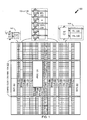
- FIG. 1 illustrates an FPGA architecture 100 that includes a large number of different programmable tiles including multi-gigabit transceivers (“MGTs") 101, configurable logic blocks (“CLBs”) 102, random access memory blocks (“BRAMs”) 103, input/output blocks (“IOBs”) 104, configuration and clocking logic (“CONFIG/CLOCKS”) 105, digital signal processing blocks (“DSPs”) 106, specialized input/output blocks (“I/O”) 107 (e.g., configuration ports and clock ports), and other programmable logic 108 such as digital clock managers, analog-to-digital converters, system monitoring logic, and so forth.
- Some FPGAs also include dedicated processor blocks (“PROC”) 110.
- PROC dedicated processor blocks
- each programmable tile includes a programmable interconnect element ("INT") 111 having standardized connections to and from a corresponding interconnect element in each adjacent tile. Therefore, the programmable interconnect elements taken together implement the programmable interconnect structure for the illustrated FPGA.
- the programmable interconnect element 111 also includes the connections to and from the programmable logic element within the same tile, as shown by the examples included at the top of FIG. 1 .
- An IOB 104 can include, for example, two instances of an input/output logic element ("IOL") 115 in addition to one instance of the programmable interconnect element 111.
- IOL input/output logic element
- the actual I/O pads connected, for example, to the I/O logic element 115 typically are not confined to the area of the input/output logic element 115.
- a columnar area near the center of the die (shown in FIG. 1 ) is used for configuration, clock, and other control logic. Horizontal areas 109 extending from this column are used to distribute the clocks and configuration signals across the breadth of the FPGA.
- Some FPGAs utilizing the architecture illustrated in FIG. 1 include additional logic blocks that disrupt the regular columnar structure making up a large part of the FPGA.
- the additional logic blocks can be programmable blocks and/or dedicated logic.
- processor block 110 spans several columns of CLBs and BRAMs.
- FIG. 1 is intended to illustrate only an exemplary FPGA architecture.
- the numbers of logic blocks in a column, the relative width of the columns, the number and order of columns, the types of logic blocks included in the columns, the relative sizes of the logic blocks, and the interconnect/logic implementations included at the top of FIG. 1 are purely exemplary.
- more than one adjacent column of CLBs is typically included wherever the CLBs appear, to facilitate the efficient implementation of user logic, but the number of adjacent CLB columns varies with the overall size of the FPGA.
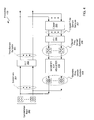
- FIG. 2 is a block diagram depicting an exemplary embodiment of a transmitter 200 of the prior art. As transmitter 200 is known, an overly detailed description of transmitter 200 is not provided for purposes of clarity. Transmitter 200 may be for OFDM/OFDMA signals, hereinafter collectively and singly referred to as OFDM signals.
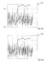
- FIG. 3A is a signal diagram depicting an exemplary embodiment of a waveform 300A having peaks 301A.
- FIG. 3B is a signal diagram depicting an exemplary embodiment of waveform 300A after having peaks 301A clipped, namely waveform 300B having peaks 301 B.
- an ACE procedure may be used. It should be appreciated that clipping of waveforms may introduce distortions in a spectral domain that violate a spectral mask and introduce adjacent channel interference. While some subcarriers may be dedicated for PAPR reduction by introducing extra symbols, namely reserve tones, to reduce PAPR, tone reservation uses up signal bandwidth and may not be compliant with some standards. An ACE procedure does not use any additional transmission bandwidth and may be implemented without having to change known standards, some of which are previously referenced herein.
- clipping may introduce distortions.
- such distortions may be observable as symbols or points of a constellation moving away from their respective location of origin.
- clipped time domain samples 207 output from clipper 205 may be provided to Fast Fourier Transform block ("FFT") 206 for providing clipped frequency domain symbols 208.
- FFT Fast Fourier Transform block
- clipped frequency domain symbols 208 have moved away from their locations of origin, which is generally indicated as more spreading of points or symbols in clipped frequency domain signals 208 as compared with constellation input 202.
- Clipped frequency domain symbols 208 may be provided to an ACE adjuster 209 to reduce constellation errors which may be relatively high and which may increase EVM.
- ACE adjuster 209 is configured to perform an ACE iteration. An ACE iteration moves symbols back to their original locations on a selective basis to produce bounded domain symbols 210. Those symbols that minimize symbol distance are moved back to their original locations, and those symbols that increase symbol distance are retained or otherwise not selected for relocation.
- Multiplexers 211 may be used for selecting between inputs 202 and 210 to IFFT 203.
- An ACE iteration by ACE adjuster 209 may cause different peaks in time domain samples with respect to those peaks input to ACE adjuster 209 represented in the frequency domain for such iteration. Accordingly, the same ACE procedure may be iterated multiple times. From the following description, it should be appreciated that EVM bounding as described herein may be applied to any of the ACE iteration techniques to limit EVM.
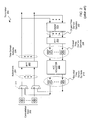
- FIG. 4 is a block diagram depicting an exemplary embodiment of a transmitter 400.
- Transmitter 400 of FIG. 4 is similar to transmitter 200 of FIG. 2 , except that ACE adjuster 209 is replaced with a "Modified ACE" adjuster (i.e., a constellation points adjustment module) 410 for producing bounded domain symbols 408. Operation of "Modified ACE" adjuster 410 is described with simultaneous reference to FIG. 4 and the respective exemplary embodiments depicted by the graphic diagrams of FIGS. 5A through 5E .
- Modified ACE adjuster
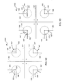
- a constellation 500 such as a constellation of clipped frequency domain symbols 208, is input to Modified ACE adjuster 410.
- a 4-QAM constellation is illustratively shown, however it should be appreciated that QAM sizes larger than four may be used.
- QAM symbols are located in one of four quadrants I through IV in a constellation map defined by real and imaginary axes 501 and 502, respectively, for complex numbers.
- points or symbols 503 closer to at least one of axis 501 and axis 502 than a point of origin 504 for a quadrant are moved or translated to the point of origin 504.
- Reference lines 505 and 506, which emanate from points of origin 504 and respectively parallel axis 501 and axis 502, are illustratively shown to more clearly identify those points 503 to be translated by an ACE iteration.
- FIG. 5B there is shown a graphic diagram depicting an exemplary embodiment of a constellation 510B, which is constellation 500 of FIG. 5A after an ACE portion or iteration of a Modified ACE algorithm.
- Points 507 and 508, as well as any symbols or points lying on points of origin 504, are unaffected by an ACE portion of a Modified ACE algorithm.
- Points 507 are in a region bounded by axes 505 and 506 for each quadrant I through IV, and thus do not lie between axes, for example between axis 506 and 502 or between axis 505 and 501.
- Points 507 and 508 may lay on axis 505 or 506.
- a bounding perimeter 511 may be defined from a radius of point of origin 504 in each of quadrants I through IV. Bounding perimeters 511 may be determined responsive to an EVM threshold level. However, after completion of an ACE portion of a Modified ACE algorithm, points or symbols between axis 501 and reference lines 505 or between axis 502 and reference lines 506, or a combination thereof, will have already been translated, and thus a portion, as generally identified by a dashed line, of each bounding perimeter 511 is not of concern. Accordingly, for each quadrant, a region or area defined by reference lines 505 and 506 and such dashed line portion of bounding perimeter 511 is not used.
- an arc 512 which in this example for a corner symbol of a constellation is for ⁇ /4 arc length, portion of perimeter 511 going from reference line 505 to reference line 506 and radially extending from point of origin 504 in each quadrant I though IV is used.
- arc length 512 and references lines 505 and 506 define a bounded region or area 520.
- Region 520 may be used to delineate which points are to be translated by a Modified ACE iteration performed by Modified ACE adjuster 410 to bound EVM to a threshold value, and which points are not.
- points 507 outside of regions 520 are to be translated to reduce EVM associated with constellation 510C and 510D and points 508 within regions 520 are not translated. It should be understood that the relative effect of points outside of regions 520 may increase EVM beyond a threshold level.
- points 507 are all translated to points of origin 504 respectively associated with a quadrant in which such points 507 are located, as generally indicated by squiggly lines with arrows. Points 507 need not necessarily be translated to respective points of origin 504 to reduce EVM to be within a threshold level.
- FIG. 5C there is illustratively shown a graphic diagram depicting an exemplary embodiment of a constellation 510C. Constellation 510C is constellation 510B of FIG. 5B , except that points 507 are translated onto borders of bounded regions 520, such as onto arc lengths 512, respectively associated with the quadrants in which such points 507 are located, as generally indicated by squiggly lines with arrows.
- points 507 may alternatively be translated or moved to locations within the peripheries of bounded regions 520, as generally illustratively shown by a graphic diagram depicting an exemplary embodiment of a constellation 510D in FIG. 5D .
- constellation 510D which is constellation 510B of FIG. 5B , expect as depicted with points 507 translated, as generally indicated by squiggly lines with arrows, to the interiors of bounded regions 520 within quadrants I through IV respectively associated with such points 507.
- points outside a bounded region 520 after a Modified ACE portion of a Modified ACE algorithm may be moved to a point of origin 504 of a bounded region 520, to a border or a periphery of a bounded region 520, or to the interior of a bounded region 520, or any combination thereof.
- points 507 are moved to points of origin 504 of respective quadrants associated with such points 507, as illustratively shown in the constellation diagram of FIGS. 5B and 5E .
- constellation 525 is illustratively shown as having all points or symbols associated with quadrants I through IV being translated to a bounded region, namely bounded region or regions 520.
- constellation 525 is constellation 510B of FIG. 5B after translating points 507 to points of origin 504.
- points 503 and 507 are translated to respective points of origin 504 on a quadrant-by-quadrant basis.
- constellation 530 is illustratively shown as having all points or symbols associated with quadrants I through IV being translated to a bounded region or regions 520.
- constellation 530 is constellation 510B of FIG. 5B after translating points 507 to points either within bounded regions 520 or on the boundary of bounded regions 520 on a quadrant-by-quadrant basis.
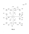
- FIG. 6 there is illustratively shown a graphic diagram depicting an exemplary embodiment of a constellation 600.
- a scattering of points or symbols is not illustratively shown in FIG. 6 .
- FIG. 6 illustratively shows bounded regions 520 and 620 for a 16-QAM embodiment.
- Bounded regions 520 are associated with corner symbols 631 through 634 at the periphery of constellation 600 are as previously described with reference to the 4-QAM embodiment of FIGS. 5A through 5E .
- bounded regions 620 are associated with other periphery locations of constellation 610, namely edge symbols 641-644 and 651-654.
- Interior symbols 621 through 624 are unaltered by Modified ACE adjuster 410 of FIG. 4 .
- Vertical edge symbols 641 through 644 have bounded regions 620 defined by intersections of reference lines 506 (parallel to axis 502) and arc sections or lengths 612.
- Arcs 612 for vertical bounded regions 620 extend from and to reference lines 506 and radially emanate away from points of origin 504.
- Vertical edge symbols 641 through 644 thus have semicircular or ⁇ /2 arcs.
- Arcs 612 of vertical bounded regions 620 in quadrants I and III extend from reference line 506 in a positive direction with respect to axis 501.
- Arcs 612 of vertical bounded regions 620 in quadrants II and IV extend from reference line 506 in a negative direction with respect to axis 501.
- Horizontal edge symbols 651 through 654 have bounded regions 620 which are defined by intersections of axis 505 (parallel to axis 501) and arcs 612.
- Arcs 612 for horizontal bounded regions 620 extend from and to reference lines 505 and radially emanate away from points of origin 504.
- Horizontal edge symbols 651 through 654 thus have semicircular or ⁇ /2 arcs.
- Arcs 612 of horizontal bounded regions 620 in quadrants I and II extend from reference line 505 in a positive direction with respect to axis 502.
- Arcs 612 of horizontal bounded regions 620 in quadrants III and IV extend from reference line 505 in a negative direction with respect to axis 502.
- FIG. 7 is a flow diagram depicting an exemplary embodiment of a signal processing flow 700.
- clipped frequency domain symbols are obtained.
- any symbols that may be moved of the symbols obtained at 701 using an ACE iteration are moved or translated at 702.
- a bounded region for an EVM target or responsive to an EVM target may be applied for determining which if any symbols after an ACE iteration performed at 702 remain outside of such bounded region as determined at 703. If any of such symbols are outside such bounded region as determined at 703, such symbols may be moved, as previously described herein, to such bounded region.
- Modified ACE adjusted frequency domain symbols of a final iteration that are IFFT converted to time domain samples may be released for transmission at 705.
- a storage array for storing time domain samples for output is not illustratively shown in FIG. 4 , it should be understood that control circuitry and arrays for storing time domain samples for transmission are known, and thus are not described herein in any unnecessary detail for purposes of clarity.
Landscapes
- Engineering & Computer Science (AREA)
- Computer Networks & Wireless Communication (AREA)
- Signal Processing (AREA)
- Digital Transmission Methods That Use Modulated Carrier Waves (AREA)
Claims (13)
- Procédé pour traiter des signaux comprenant des symboles situés dans des quadrants d'une carte de constellation définie par des axes réel et imaginaire (501, 502), ledit procédé comprenant :l'exécution d'une procédure d'extension de constellation active, ACE, sur un premier ensemble desdits symboles, dans lequel, pour chaque quadrant, chaque symbole déplacé pendant la procédure ACE est déplacé vers des axes concourants perpendiculaires (505, 506) dans le quadrant, lesdits axes concourants étant parallèles aux dits axes réel et imaginaire, ledit procédé étant caractérisé en outre par :la délimitation, pour chaque quadrant, d'une région établie par les axes concourants par un arc (512) ;l'identification, pour chaque quadrant, de symboles à l'extérieur de l'arc de la région délimitée après la procédure ACE, dans lequel la région délimitée est déterminée en réponse à une amplitude cible de vecteur d'erreur ;la translation, pour chaque quadrant, des symboles identifiés vers la région délimitée ;la détermination d'un rapport de puissance crête sur puissance moyenne après la translation des symboles identifiés vers les régions délimitées ; etla détermination s'il convient d'effectuer ou non une autre procédure ACE sur la base de la valeur déterminée dudit rapport de puissance crête sur puissance moyenne.
- Procédé selon la revendication 1, dans lequel les symboles identifiés sont déplacés vers un emplacement d'origine de la région délimitée, ladite origine étant le point d'intersection desdits axes concourants.
- Procédé selon la revendication 1 ou 2, comprenant en outre :avant l'exécution de la procédure ACE, l'obtention des symboles d'une constellation, dans lequel la procédure ACE est appliquée aux symboles de la constellation.
- Procédé selon l'une quelconque des revendications 1 à 3, comprenant en outre :l'obtention d'un autre ensemble de symboles de la constellation ; etl'exécution de la procédure ACE sur l'autre ensemble de symboles de la constellation.
- Procédé selon la revendication 3 ou 4, dans lequel la constellation est au moins un ensemble de modulation d'amplitude en quadrature à 4 états, 4-QAM.
- Procédé selon l'une quelconque des revendications 1 à 5, dans lequel la région délimitée est destinée à une région de symboles de bord de la constellation.
- Procédé selon la revendication 6, dans lequel la région de symboles de bord est une région de symboles de coin de la constellation.
- Procédé selon l'une quelconque des revendications 1 à 7, dans lequel les symboles sont déplacés vers un bord de la région délimitée.
- Procédé selon l'une quelconque des revendications 1 à 7, dans lequel les symboles sont déplacés à l'intérieur ou sur un bord de la région délimitée.
- Emetteur, comprenant :un module d'ajustement de points de constellation, dans lequel le module d'ajustement de points de constellation est configuré pour :effectuer une procédure d'extension de constellation active, ACE, sur un premier ensemble de points de constellation d'une carte de constellation définie par des axes réel et imaginaire (501, 502), où, pour chaque quadrant, chaque point de constellation déplacé pendant la procédure ACE est déplacé vers des axes concourants (505, 506) dans le quadrant, lesdits axes concourants étant parallèles aux dits axes réel et imaginaire, ledit émetteur étant caractérisé en ce que ledit module d'ajustement de points de constellation est en outre configuré pour :délimiter, pour chaque quadrant, une région établie par les axes concourants par un arc (512),identifier, pour chaque quadrant, les points de constellation de la constellation restant à l'extérieur de l'arc de la région délimitée et translater lesdits points identifiés vers la région délimitée, dans lequel la région délimitée est définie pour limiter l'amplitude de vecteur d'erreur à un niveau de seuil ;déterminer un rapport puissance crête sur puissance moyenne après la translation des points de constellation identifiés vers les régions délimitées ; etdéterminer s'il convient d'effectuer ou non une autre procédure ACE sur la base du rapport puissance crête sur puissance moyenne.
- Emetteur selon la revendication 10, dans lequel le module d'ajustement de points de constellation est configuré pour ajuster uniquement les points de constellation qui se trouvent à une périphérie de la constellation.
- Emetteur selon l'une quelconque des revendications 10 et 11, dans lequel l'émetteur est configuré pour effectuer une modulation sélectionnée dans un groupe consistant en un multiplexage par répartition en fréquences orthogonales et un accès multiple par répartition en fréquences orthogonales.
- Emetteur selon la revendication 12, dans lequel :le niveau de seuil est pour une norme selon IEEE 802.16e.
Applications Claiming Priority (2)
| Application Number | Priority Date | Filing Date | Title |
|---|---|---|---|
| US12/430,863 US8831117B2 (en) | 2009-04-27 | 2009-04-27 | Peak-to-average power ratio reduction with bounded error vector magnitude |
| PCT/US2010/032127 WO2010129190A2 (fr) | 2009-04-27 | 2010-04-22 | Réduction de rapport de puissance de crête/puissance moyenne avec amplitude de vecteur d'erreur liée |
Publications (2)
| Publication Number | Publication Date |
|---|---|
| EP2425598A2 EP2425598A2 (fr) | 2012-03-07 |
| EP2425598B1 true EP2425598B1 (fr) | 2015-01-21 |
Family
ID=42557358
Family Applications (1)
| Application Number | Title | Priority Date | Filing Date |
|---|---|---|---|
| EP10720480.2A Active EP2425598B1 (fr) | 2009-04-27 | 2010-04-22 | Réduction du rapport puissance de crête à puissance moyenne, papr, avec limitation de l'amplitude du vecteur d'erreur |
Country Status (6)
| Country | Link |
|---|---|
| US (1) | US8831117B2 (fr) |
| EP (1) | EP2425598B1 (fr) |
| JP (1) | JP5616959B2 (fr) |
| KR (1) | KR101333469B1 (fr) |
| CN (1) | CN102439933B (fr) |
| WO (1) | WO2010129190A2 (fr) |
Cited By (1)
| Publication number | Priority date | Publication date | Assignee | Title |
|---|---|---|---|---|
| CN110336763A (zh) * | 2019-05-21 | 2019-10-15 | 西安电子科技大学 | 一种抑制高阶调制ofdm信号峰均比的ace的方法及系统 |
Families Citing this family (12)
| Publication number | Priority date | Publication date | Assignee | Title |
|---|---|---|---|---|
| KR100854064B1 (ko) * | 2006-12-05 | 2008-08-25 | 한국전자통신연구원 | 직교 주파수 분할 다중화 시스템에서 papr감소를 위한송신장치 및 방법 |
| US8693888B2 (en) | 2012-01-10 | 2014-04-08 | Alcatel Lucent | Noise-resilient constellations for an optical transport system |
| US8897655B2 (en) * | 2012-06-18 | 2014-11-25 | Alcatel Lucent | Adaptive constellations and decision regions for an optical transport system |
| JP2015080089A (ja) * | 2013-10-17 | 2015-04-23 | インターナショナル・ビジネス・マシーンズ・コーポレーションInternational Business Machines Corporation | 送信装置、通信システム、回路装置、通信方法およびプログラム(直流インバランスを補償するための強調された信号点配置操作) |
| US9100115B1 (en) | 2014-03-28 | 2015-08-04 | Freescale Semiconductor, Inc. | Processor unit for determining a quality indicator of a communication channel and a method thereof |
| US9444669B2 (en) * | 2014-12-30 | 2016-09-13 | Texas Instruments Incorporated | Peak to average power ratio reduction of OFDM signals |
| CN107690785B (zh) | 2015-04-30 | 2021-06-29 | 交互数字麦迪逊专利控股公司 | 用于降低信号中的峰均功率比的装置和方法 |
| EP3089417A1 (fr) * | 2015-04-30 | 2016-11-02 | Thomson Licensing | Procédé et appareil de réduction du rapport de puissance pic-moyenne d'un signal |
| EP3223446A1 (fr) * | 2016-03-22 | 2017-09-27 | Xieon Networks S.à r.l. | Procédé de protection d'une liaison dans un réseau optique |
| US10680592B2 (en) | 2017-10-19 | 2020-06-09 | Xilinx, Inc. | Quadrature clock correction circuit for transmitters |
| US11863359B1 (en) * | 2021-05-11 | 2024-01-02 | Amazon Technologies, Inc. | Subcarrier pre-equalization technology for frequency selective fading characteristics of wireless channels |
| US20240348487A1 (en) * | 2021-07-26 | 2024-10-17 | Telefonaktiebolaget Lm Ericsson (Publ) | Methods and apparatuses for adaptation of communication parameter |
Family Cites Families (10)
| Publication number | Priority date | Publication date | Assignee | Title |
|---|---|---|---|---|
| US7058369B1 (en) * | 2001-11-21 | 2006-06-06 | Pmc-Sierra Inc. | Constant gain digital predistortion controller for linearization of non-linear amplifiers |
| US20050141642A1 (en) * | 2002-06-28 | 2005-06-30 | Advantest Corporation | Transformer, transforming apparatus, transforming method and machine readable medium storing thereon program |
| JPWO2005055479A1 (ja) | 2003-12-02 | 2007-07-05 | 松下電器産業株式会社 | マルチキャリア伝送における無線送信装置およびピーク電力抑圧方法 |
| JP4436410B2 (ja) * | 2004-03-12 | 2010-03-24 | 株式会社エヌ・ティ・ティ・ドコモ | クリッピングおよび修正されたコンステレーションを使用するofdmにおけるピーク低減 |
| US7313373B1 (en) * | 2005-04-21 | 2007-12-25 | Xilinx, Inc. | Crest factor reduction for use in a multiband transmitter |
| US7944991B2 (en) * | 2005-10-27 | 2011-05-17 | Georgia Tech Research Corporation | Constrained clipping for peak-to-average power ratio (crest factor) reduction in multicarrier transmission systems |
| CN101202726A (zh) * | 2006-12-14 | 2008-06-18 | 中兴通讯股份有限公司 | 基于星座扩展和空余子载波降低ofdm中峰均比的方法 |
| CN101374126B (zh) * | 2007-08-24 | 2012-07-18 | 中兴通讯股份有限公司 | 一种正交频分复用系统峰均功率比抑制方法 |
| JP5085351B2 (ja) | 2008-01-25 | 2012-11-28 | 株式会社エヌ・ティ・ティ・ドコモ | 移動通信システムにおける送信装置及び方法 |
| CN101227446B (zh) * | 2008-02-01 | 2012-01-25 | 成都途筏达科技有限公司 | 一种基于自适应evm的信号峰均比降低方法 |
-
2009
- 2009-04-27 US US12/430,863 patent/US8831117B2/en active Active
-
2010
- 2010-04-22 KR KR1020117026748A patent/KR101333469B1/ko active Active
- 2010-04-22 CN CN201080018623.1A patent/CN102439933B/zh active Active
- 2010-04-22 JP JP2012508546A patent/JP5616959B2/ja active Active
- 2010-04-22 EP EP10720480.2A patent/EP2425598B1/fr active Active
- 2010-04-22 WO PCT/US2010/032127 patent/WO2010129190A2/fr not_active Ceased
Cited By (2)
| Publication number | Priority date | Publication date | Assignee | Title |
|---|---|---|---|---|
| CN110336763A (zh) * | 2019-05-21 | 2019-10-15 | 西安电子科技大学 | 一种抑制高阶调制ofdm信号峰均比的ace的方法及系统 |
| CN110336763B (zh) * | 2019-05-21 | 2021-08-17 | 西安电子科技大学 | 一种抑制高阶调制ofdm信号峰均比的ace的方法及系统 |
Also Published As
| Publication number | Publication date |
|---|---|
| JP2012525776A (ja) | 2012-10-22 |
| US8831117B2 (en) | 2014-09-09 |
| EP2425598A2 (fr) | 2012-03-07 |
| KR20120018312A (ko) | 2012-03-02 |
| WO2010129190A3 (fr) | 2010-12-29 |
| CN102439933B (zh) | 2014-08-13 |
| KR101333469B1 (ko) | 2013-11-26 |
| JP5616959B2 (ja) | 2014-10-29 |
| WO2010129190A2 (fr) | 2010-11-11 |
| CN102439933A (zh) | 2012-05-02 |
| US20100272195A1 (en) | 2010-10-28 |
Similar Documents
| Publication | Publication Date | Title |
|---|---|---|
| EP2425598B1 (fr) | Réduction du rapport puissance de crête à puissance moyenne, papr, avec limitation de l'amplitude du vecteur d'erreur | |
| EP3314837B1 (fr) | Pré-distorsion numérique pouvant s'adapter à la forme d'onde | |
| US8666336B1 (en) | Digital pre-distortion with model-based order estimation | |
| JP4685860B2 (ja) | マルチキャリア変調システムにおける改善 | |
| KR20120127504A (ko) | 파일럿 톤 보조 선택 맵핑을 위한 시스템 및 방법 | |
| Wittig et al. | Modem design in the era of 5G and beyond: The need for a formal approach | |
| Song et al. | A low-complexity peak cancellation scheme and its FPGA implementation for peak-to-average power ratio reduction | |
| US10149181B2 (en) | Signal output apparatus, board, and signal output method | |
| Tran | Hybrid scheme using modified tone reservation and clipping-and-filtering methods for peak-to-average power ratio reduction of OFDM signals | |
| US11108364B1 (en) | System and method for digital pre-distortion circuits | |
| CN106063212A (zh) | 用于在无线通信系统中生成非高斯干扰信道的方法和设备 | |
| Dang et al. | Active constellation modification technique for PAPR reduction of OFDM signals | |
| Iqbal et al. | Selective mapping: Implementation of PAPR reduction technique in OFDM on SDR platform | |
| Cavalcante et al. | A flexible peak-to-average power ratio reduction scheme for OFDM systems by the adaptive projected subgradient method | |
| Keerthana et al. | FPGA implementation of FBMC baseband modular for 5G wireless communication | |
| Mohamed et al. | A Novel implementation of OFDM using FPGA | |
| Kumar et al. | FPGA Implementation of OFDM Transceiver using Verilog-Hardware Description Language | |
| Ahmad et al. | VLSI Implementation of OFDM Transmitter chain for 4G Communication | |
| Martín Gutiérrez | Implementació en una FPGA d'un sistema de Tx/Rx OFDM | |
| Kumar et al. | Reducing the peak-to-average power ration for NOMA waveform with diverse channel using micro genetic algorithm-based partial transmission sequence algorithm | |
| Abdel‐Atty et al. | VHDL implementation of circular shifting‐partial transmit sequence in MIMO OFDM systems | |
| Ferreira et al. | A dynamically reconfigurable dual-waveform baseband modulator for flexible wireless communications | |
| EP3136200A1 (fr) | Procédé et appareil pour fournir un vecteur échantillon représentant au moins une partie d'un signal modulé à porteuses multiples | |
| GB2575118A (en) | Dynamic scaling of channel state information | |
| Jang et al. | Low-power FFT design for NC-OFDM in cognitive radio systems |
Legal Events
| Date | Code | Title | Description |
|---|---|---|---|
| PUAI | Public reference made under article 153(3) epc to a published international application that has entered the european phase |
Free format text: ORIGINAL CODE: 0009012 |
|
| 17P | Request for examination filed |
Effective date: 20111021 |
|
| AK | Designated contracting states |
Kind code of ref document: A2 Designated state(s): AT BE BG CH CY CZ DE DK EE ES FI FR GB GR HR HU IE IS IT LI LT LU LV MC MK MT NL NO PL PT RO SE SI SK SM TR |
|
| DAX | Request for extension of the european patent (deleted) | ||
| 17Q | First examination report despatched |
Effective date: 20120823 |
|
| GRAP | Despatch of communication of intention to grant a patent |
Free format text: ORIGINAL CODE: EPIDOSNIGR1 |
|
| INTG | Intention to grant announced |
Effective date: 20140812 |
|
| RIN1 | Information on inventor provided before grant (corrected) |
Inventor name: RAO, RAGHAVENDAR, M. Inventor name: DICK, CHRISTOPHER, H. |
|
| GRAS | Grant fee paid |
Free format text: ORIGINAL CODE: EPIDOSNIGR3 |
|
| GRAA | (expected) grant |
Free format text: ORIGINAL CODE: 0009210 |
|
| AK | Designated contracting states |
Kind code of ref document: B1 Designated state(s): AT BE BG CH CY CZ DE DK EE ES FI FR GB GR HR HU IE IS IT LI LT LU LV MC MK MT NL NO PL PT RO SE SI SK SM TR |
|
| REG | Reference to a national code |
Ref country code: GB Ref legal event code: FG4D |
|
| REG | Reference to a national code |
Ref country code: CH Ref legal event code: EP |
|
| REG | Reference to a national code |
Ref country code: IE Ref legal event code: FG4D |
|
| REG | Reference to a national code |
Ref country code: DE Ref legal event code: R096 Ref document number: 602010021948 Country of ref document: DE Effective date: 20150305 |
|
| REG | Reference to a national code |
Ref country code: AT Ref legal event code: REF Ref document number: 709582 Country of ref document: AT Kind code of ref document: T Effective date: 20150315 |
|
| REG | Reference to a national code |
Ref country code: NL Ref legal event code: VDEP Effective date: 20150121 |
|
| REG | Reference to a national code |
Ref country code: AT Ref legal event code: MK05 Ref document number: 709582 Country of ref document: AT Kind code of ref document: T Effective date: 20150121 |
|
| REG | Reference to a national code |
Ref country code: LT Ref legal event code: MG4D |
|
| PG25 | Lapsed in a contracting state [announced via postgrant information from national office to epo] |
Ref country code: FI Free format text: LAPSE BECAUSE OF FAILURE TO SUBMIT A TRANSLATION OF THE DESCRIPTION OR TO PAY THE FEE WITHIN THE PRESCRIBED TIME-LIMIT Effective date: 20150121 Ref country code: SE Free format text: LAPSE BECAUSE OF FAILURE TO SUBMIT A TRANSLATION OF THE DESCRIPTION OR TO PAY THE FEE WITHIN THE PRESCRIBED TIME-LIMIT Effective date: 20150121 Ref country code: ES Free format text: LAPSE BECAUSE OF FAILURE TO SUBMIT A TRANSLATION OF THE DESCRIPTION OR TO PAY THE FEE WITHIN THE PRESCRIBED TIME-LIMIT Effective date: 20150121 Ref country code: LT Free format text: LAPSE BECAUSE OF FAILURE TO SUBMIT A TRANSLATION OF THE DESCRIPTION OR TO PAY THE FEE WITHIN THE PRESCRIBED TIME-LIMIT Effective date: 20150121 Ref country code: NO Free format text: LAPSE BECAUSE OF FAILURE TO SUBMIT A TRANSLATION OF THE DESCRIPTION OR TO PAY THE FEE WITHIN THE PRESCRIBED TIME-LIMIT Effective date: 20150421 Ref country code: HR Free format text: LAPSE BECAUSE OF FAILURE TO SUBMIT A TRANSLATION OF THE DESCRIPTION OR TO PAY THE FEE WITHIN THE PRESCRIBED TIME-LIMIT Effective date: 20150121 Ref country code: BG Free format text: LAPSE BECAUSE OF FAILURE TO SUBMIT A TRANSLATION OF THE DESCRIPTION OR TO PAY THE FEE WITHIN THE PRESCRIBED TIME-LIMIT Effective date: 20150421 |
|
| PG25 | Lapsed in a contracting state [announced via postgrant information from national office to epo] |
Ref country code: AT Free format text: LAPSE BECAUSE OF FAILURE TO SUBMIT A TRANSLATION OF THE DESCRIPTION OR TO PAY THE FEE WITHIN THE PRESCRIBED TIME-LIMIT Effective date: 20150121 Ref country code: GR Free format text: LAPSE BECAUSE OF FAILURE TO SUBMIT A TRANSLATION OF THE DESCRIPTION OR TO PAY THE FEE WITHIN THE PRESCRIBED TIME-LIMIT Effective date: 20150422 Ref country code: NL Free format text: LAPSE BECAUSE OF FAILURE TO SUBMIT A TRANSLATION OF THE DESCRIPTION OR TO PAY THE FEE WITHIN THE PRESCRIBED TIME-LIMIT Effective date: 20150121 Ref country code: LV Free format text: LAPSE BECAUSE OF FAILURE TO SUBMIT A TRANSLATION OF THE DESCRIPTION OR TO PAY THE FEE WITHIN THE PRESCRIBED TIME-LIMIT Effective date: 20150121 Ref country code: PL Free format text: LAPSE BECAUSE OF FAILURE TO SUBMIT A TRANSLATION OF THE DESCRIPTION OR TO PAY THE FEE WITHIN THE PRESCRIBED TIME-LIMIT Effective date: 20150121 Ref country code: IS Free format text: LAPSE BECAUSE OF FAILURE TO SUBMIT A TRANSLATION OF THE DESCRIPTION OR TO PAY THE FEE WITHIN THE PRESCRIBED TIME-LIMIT Effective date: 20150521 |
|
| REG | Reference to a national code |
Ref country code: DE Ref legal event code: R097 Ref document number: 602010021948 Country of ref document: DE |
|
| PG25 | Lapsed in a contracting state [announced via postgrant information from national office to epo] |
Ref country code: DK Free format text: LAPSE BECAUSE OF FAILURE TO SUBMIT A TRANSLATION OF THE DESCRIPTION OR TO PAY THE FEE WITHIN THE PRESCRIBED TIME-LIMIT Effective date: 20150121 Ref country code: CZ Free format text: LAPSE BECAUSE OF FAILURE TO SUBMIT A TRANSLATION OF THE DESCRIPTION OR TO PAY THE FEE WITHIN THE PRESCRIBED TIME-LIMIT Effective date: 20150121 Ref country code: RO Free format text: LAPSE BECAUSE OF FAILURE TO SUBMIT A TRANSLATION OF THE DESCRIPTION OR TO PAY THE FEE WITHIN THE PRESCRIBED TIME-LIMIT Effective date: 20150121 Ref country code: SK Free format text: LAPSE BECAUSE OF FAILURE TO SUBMIT A TRANSLATION OF THE DESCRIPTION OR TO PAY THE FEE WITHIN THE PRESCRIBED TIME-LIMIT Effective date: 20150121 Ref country code: EE Free format text: LAPSE BECAUSE OF FAILURE TO SUBMIT A TRANSLATION OF THE DESCRIPTION OR TO PAY THE FEE WITHIN THE PRESCRIBED TIME-LIMIT Effective date: 20150121 |
|
| PLBE | No opposition filed within time limit |
Free format text: ORIGINAL CODE: 0009261 |
|
| STAA | Information on the status of an ep patent application or granted ep patent |
Free format text: STATUS: NO OPPOSITION FILED WITHIN TIME LIMIT |
|
| PG25 | Lapsed in a contracting state [announced via postgrant information from national office to epo] |
Ref country code: MC Free format text: LAPSE BECAUSE OF FAILURE TO SUBMIT A TRANSLATION OF THE DESCRIPTION OR TO PAY THE FEE WITHIN THE PRESCRIBED TIME-LIMIT Effective date: 20150121 Ref country code: LU Free format text: LAPSE BECAUSE OF FAILURE TO SUBMIT A TRANSLATION OF THE DESCRIPTION OR TO PAY THE FEE WITHIN THE PRESCRIBED TIME-LIMIT Effective date: 20150422 |
|
| REG | Reference to a national code |
Ref country code: CH Ref legal event code: PL |
|
| 26N | No opposition filed |
Effective date: 20151022 |
|
| PG25 | Lapsed in a contracting state [announced via postgrant information from national office to epo] |
Ref country code: IT Free format text: LAPSE BECAUSE OF FAILURE TO SUBMIT A TRANSLATION OF THE DESCRIPTION OR TO PAY THE FEE WITHIN THE PRESCRIBED TIME-LIMIT Effective date: 20150121 |
|
| PG25 | Lapsed in a contracting state [announced via postgrant information from national office to epo] |
Ref country code: CH Free format text: LAPSE BECAUSE OF NON-PAYMENT OF DUE FEES Effective date: 20150430 Ref country code: LI Free format text: LAPSE BECAUSE OF NON-PAYMENT OF DUE FEES Effective date: 20150430 |
|
| PG25 | Lapsed in a contracting state [announced via postgrant information from national office to epo] |
Ref country code: SI Free format text: LAPSE BECAUSE OF FAILURE TO SUBMIT A TRANSLATION OF THE DESCRIPTION OR TO PAY THE FEE WITHIN THE PRESCRIBED TIME-LIMIT Effective date: 20150121 |
|
| REG | Reference to a national code |
Ref country code: FR Ref legal event code: PLFP Year of fee payment: 7 |
|
| PG25 | Lapsed in a contracting state [announced via postgrant information from national office to epo] |
Ref country code: BE Free format text: LAPSE BECAUSE OF FAILURE TO SUBMIT A TRANSLATION OF THE DESCRIPTION OR TO PAY THE FEE WITHIN THE PRESCRIBED TIME-LIMIT Effective date: 20150121 |
|
| PG25 | Lapsed in a contracting state [announced via postgrant information from national office to epo] |
Ref country code: MT Free format text: LAPSE BECAUSE OF FAILURE TO SUBMIT A TRANSLATION OF THE DESCRIPTION OR TO PAY THE FEE WITHIN THE PRESCRIBED TIME-LIMIT Effective date: 20150121 |
|
| REG | Reference to a national code |
Ref country code: FR Ref legal event code: PLFP Year of fee payment: 8 |
|
| PG25 | Lapsed in a contracting state [announced via postgrant information from national office to epo] |
Ref country code: SM Free format text: LAPSE BECAUSE OF FAILURE TO SUBMIT A TRANSLATION OF THE DESCRIPTION OR TO PAY THE FEE WITHIN THE PRESCRIBED TIME-LIMIT Effective date: 20150121 Ref country code: HU Free format text: LAPSE BECAUSE OF FAILURE TO SUBMIT A TRANSLATION OF THE DESCRIPTION OR TO PAY THE FEE WITHIN THE PRESCRIBED TIME-LIMIT; INVALID AB INITIO Effective date: 20100422 |
|
| PG25 | Lapsed in a contracting state [announced via postgrant information from national office to epo] |
Ref country code: CY Free format text: LAPSE BECAUSE OF FAILURE TO SUBMIT A TRANSLATION OF THE DESCRIPTION OR TO PAY THE FEE WITHIN THE PRESCRIBED TIME-LIMIT Effective date: 20150121 |
|
| PG25 | Lapsed in a contracting state [announced via postgrant information from national office to epo] |
Ref country code: PT Free format text: LAPSE BECAUSE OF FAILURE TO SUBMIT A TRANSLATION OF THE DESCRIPTION OR TO PAY THE FEE WITHIN THE PRESCRIBED TIME-LIMIT Effective date: 20150521 |
|
| PG25 | Lapsed in a contracting state [announced via postgrant information from national office to epo] |
Ref country code: TR Free format text: LAPSE BECAUSE OF FAILURE TO SUBMIT A TRANSLATION OF THE DESCRIPTION OR TO PAY THE FEE WITHIN THE PRESCRIBED TIME-LIMIT Effective date: 20150121 |
|
| REG | Reference to a national code |
Ref country code: FR Ref legal event code: PLFP Year of fee payment: 9 |
|
| PG25 | Lapsed in a contracting state [announced via postgrant information from national office to epo] |
Ref country code: MK Free format text: LAPSE BECAUSE OF FAILURE TO SUBMIT A TRANSLATION OF THE DESCRIPTION OR TO PAY THE FEE WITHIN THE PRESCRIBED TIME-LIMIT Effective date: 20150121 |
|
| P01 | Opt-out of the competence of the unified patent court (upc) registered |
Effective date: 20230530 |
|
| PGFP | Annual fee paid to national office [announced via postgrant information from national office to epo] |
Ref country code: IE Payment date: 20240411 Year of fee payment: 15 |
|
| PGFP | Annual fee paid to national office [announced via postgrant information from national office to epo] |
Ref country code: DE Payment date: 20250313 Year of fee payment: 16 |
|
| PGFP | Annual fee paid to national office [announced via postgrant information from national office to epo] |
Ref country code: GB Payment date: 20250415 Year of fee payment: 16 |
|
| PGFP | Annual fee paid to national office [announced via postgrant information from national office to epo] |
Ref country code: FR Payment date: 20250407 Year of fee payment: 16 |