EP2425266B1 - Electrical and opto-electrical characterisation of large-area semiconductor devices - Google Patents
Electrical and opto-electrical characterisation of large-area semiconductor devices Download PDFInfo
- Publication number
- EP2425266B1 EP2425266B1 EP10714891.8A EP10714891A EP2425266B1 EP 2425266 B1 EP2425266 B1 EP 2425266B1 EP 10714891 A EP10714891 A EP 10714891A EP 2425266 B1 EP2425266 B1 EP 2425266B1
- Authority
- EP
- European Patent Office
- Prior art keywords
- electrode
- electrical
- semiconductor device
- electrode assembly
- electrolyte solution
- Prior art date
- Legal status (The legal status is an assumption and is not a legal conclusion. Google has not performed a legal analysis and makes no representation as to the accuracy of the status listed.)
- Not-in-force
Links
Images


Classifications
-
- H—ELECTRICITY
- H10—SEMICONDUCTOR DEVICES; ELECTRIC SOLID-STATE DEVICES NOT OTHERWISE PROVIDED FOR
- H10P—GENERIC PROCESSES OR APPARATUS FOR THE MANUFACTURE OR TREATMENT OF DEVICES COVERED BY CLASS H10
- H10P74/00—Testing or measuring during manufacture or treatment of wafers, substrates or devices
- H10P74/20—Testing or measuring during manufacture or treatment of wafers, substrates or devices characterised by the properties tested or measured, e.g. structural or electrical properties
- H10P74/207—Electrical properties, e.g. testing or measuring of resistance, deep levels or capacitance-voltage characteristics
Definitions
- the present invention relates to a method and device for the electrical and opto-electrical characterisation of large-area semiconductor devices. More particularly, it relates to the characterisation of such semiconductor devices in industrial production lines.
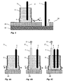
- FIG. 1 shows an example of a solar cell in the form of a cross section of the structure of a thin film Cu(In,Ga)(S,Se) 2 (referred to as CIGS in the following) solar cell 1.
- the individual layers of the structure are deposited in sequence on a glass substrate 11.
- a molybdenum conducting layer 12 provides electrical contact to the backside of the structure.
- a light absorbing p-type semiconductor layer 13 On top of the molybdenum is a light absorbing p-type semiconductor layer 13, which may be selected from CIGS.
- a semiconductor buffer layer 14 which may be selected from CdS, and on top of this are the transparent window layers 15 and 16, comprising firstly an un-intentionally doped ZnO layer 15, and an intentionally doped zinc oxide layer 16.
- All layers are important and precise control of the deposition conditions is needed to obtain the required properties from the layers to make an efficient solar device.
- One problem is achieving the desired control over large areas, which for solar cell applications typically may be of the order of one or more square metres.
- a typical solar cell production process is shown in Figs 2a through 2f .
- a molybdenum conducting layer 22 serving as a back electrode is deposited on a glass substrate 21 ( Fig 2a ).
- a subsequent P1 scribe in step (b) removes the Mo layer 22 in a defined area ( Fig 2b ).
- the light-absorbing Cu(In,Ga)(S,Se) 2 p-type semiconductor layer 23 is deposited ( Fig 2c ).
- buffer layers such as cadmium sulphide layer 24 are deposited in step (d), as shown in Fig.
- step (e) the transparent window layer 25 comprising un-intentionally doped zinc oxide is deposited on top of the CdS buffer layer 24 ( Fig 2e ).
- step (f) removes all deposited layers 23 through 25 until the Mo conducting layer 22 is exposed in a defined area 26 ( Fig 2f ).
- a final intentionally doped zinc oxide layer may be added to the stack connecting two individual cells.
- the semiconductor layers must be physically electrically contacted both on the front and back sides.
- the p-type semiconductor backside is normally deposited on top of a conducting substrate or conducting layer providing a contact at the back.
- the semiconductor front side must also be contacted to allow for testing.
- One way to contact the semiconductor front side is to use a solution which is electrically conducting, which itself can be "contacted” by an external electrode, such as platinum.
- the solution provides a transparent electrical contact which investigative light can be passed through to interrogate the semiconductor.
- This general technique is known as "photoelectrochemistry” and is somewhat known in the literature ( Dale P J et al., 2007 ECS transactions 6 ; and Duffy N W et al., 2002 J. Electroanal. Chem. 532 207-14 ).
- Once the semiconductor is electrically contacted light can be shone on to it and the opto-electrical properties of the layer can be established.
- This solution provides a front side contact which is extremely easy to remove, e.g. by just washing it away, or if the contacting solution is chosen correctly, could form part of the cell making process.
- the present invention aims to overcome or at least alleviate the disadvantages of the characterisation methods and apparatus known from the prior art.
- the present invention also aims to provide an electrical and/or opto-electrical characterisation method that can be used during the production of large-area semiconductor devices.
- the present invention proposes an electrical and/or and opto-electrical characterisation method for testing large-area semiconductor devices in production, the method comprising the steps of:
- the method may further comprise the step of providing an optical wave-guide, and immersing the wave guide in the electrolyte solution, placing it in vicinity of the top surface of the semiconductor device.
- the method may further comprise the step of providing pulsed illumination to the wave-guide.
- the method may further comprise providing a third electrode, immersing the third electrode into the electrolyte solution that places it into electrical contact with the top surface of the semiconductor device.
- the electrical measurements may comprise photoelectric measurements.
- the electrolyte solution may be a solution of europium.
- the step of scanning the movable electrode assembly relative to the surface of the semiconductor device may comprise moving the movable electrode assembly.
- the step of scanning the movable electrode assembly relative to the surface of the semiconductor device may comprise moving the first electrode in conjunction with the electrode assembly.
- a device for the electrical and/or opto-electrical characterisation of large-area semiconductor devices in production comprises:
- the movable electrode assembly may further comprises an optical wave guide optically connectable to a light source.
- the movable electrode assembly may further comprises a third electrode, the third electrode immersed into the electrolyte solution for placing it into electrical contact with the top surface of the semiconductor device.
- the wave guide may receive pulsed illumination from a light source.
- the electrolyte solution may be a solution of europium.
- the first electrode may be adapted for being moved together with the electrode assembly whilst scanning the top surface of the semiconductor device.
- the first electrode may be one of a mechanical scribe or a separate electrode following a scribe.
- the present invention proposes utilising photoelectrochemistry to characterise large area solar cells known as modules for electric and/or opto-electrical characterisation during the production process.
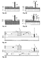
- FIG. 3 illustrates schematically how a module could be tested mid production process in accordance with the present invention.
- a back contact to a first conducting layer 32 is made by a first electrode 1 through a contact area, or contact window, 36, in which the conducting layer is directly accessible.
- the contact window 36 could advantageously be a Molybdenum P2 scribe path, either by utilizing the mechanical scribe itself as the first electrode 1, or by using a dedicated electrode 1 following it.
- An electrolyte solution 4 is held within a tube or container 6 which also comprises a second electrode 2.
- the tube 6 is placed on top of the surface of the semiconductor device, such that the electrolyte solution 4 provides the electrical contact between the top surface 35 of the semiconductor device 30 and the second electrode 2.
- the top electrode assembly 5 can then be scanned across the surface 35 of the semi-completed module 30, in a plane parallel to its top surface 35, to characterise its electrical performance.
- the present invention proposes an electrical and/or opto-electrical characterisation method for testing semiconductor devices in production.
- the semiconductor device comprises a conducting layer 32.
- This conducting layer may either be a first metallic contact layer, such as Mo, or a conducting substrate.
- the semiconductor device further comprises at least one semiconductor layer 35 deposited on the conducting layer. At least a first contact area or contact window 36' is provided, such that the conducting layer 32 of the semiconductor device can be contacted electrically. It is of course understood that the invention is equally applicable to the semiconductor device comprising several layers.
- the electrode assembly 5 shown in Fig 3 and Fig 4A while providing for the scanning of large areas, allows current-voltage characteristics to be measured.
- FIG. 4B A more advantageous electrode assembly 5' that allows opto-electrical measurements to be carried out, is shown in Fig 4B .
- an optical wave guide 7 is provided such that its proximal end can be coupled to a light source 8.
- the distal end of the wave guide 7 is positioned low in the tube 6 which contains the electrolyte solution and enables light to be shone onto the top surface of semiconductor layer 45.
- the light source 8 may provide continuous light, it is usually preferred to use a pulsed light source when performing the opto-electrical characterisation of semiconductor devices.
- the light source 8 provides pulsed illumination, e.g by using a chopper 74, photoelectric measurements can be carried out.
- Such measurements can comprise, but are not limited to: dark current, light induced current as a function of wavelength, and or light intensity.
- Fig 4C illustrates a preferred embodiment of electrode assembly 5", in which a third electrode 3 is arranged in tube 6 in addition to the second electrode 2 and the optical wave guide 7.
- the electrolyte solution 4 contained in the tube 6 also establishes an electrical contact between electrode 3 and the top surface of the semiconductor layer 45.
- the third electrode 3 may advantageously be used to influence the electrical potential at the surface of the semiconductor device.
- a suitable electrolyte 4 e.g. via its redox potential.
- a preferred electrolyte solution is a solution of europium. It is moreover of advantage that the electrolyte be easily removable from the semiconductor surface.
- the electrolyte 4 could preferably contain ions the same as those used in the following semiconductor layer.
- the present invention foresees that a first electrode 1 is placed into electrical contact with the first contact area 56 of the conducting layer 52.
- Figs 5A to 5D show examples of how the electrical contact may be established.
- a conducting layer 52 is deposited on top of a non-conducting substrate 51.
- a contact window 56 is provided in the at least one semiconductor layer 55 deposited on top of conducting layer 52.
- First electrode 1 establishes the electrical contact to the conducting layer 52 within the confines of contact window 56.
- Fig 5B shows a very similar semiconductor in which non-conducting substrate 51', conducting layer 52' and at least one semiconductor layer 55' are as describe with reference to Fig 5A .
- the contact area 56' is elongated and allows the first electrode to move along exposed part of the conducting layer 52'.
- a conducting substrate 52" is shown in Fig 5C , on top of which at least one semiconductor layer 55" has been deposited.
- a contact area 56" exposes the top surface of conducting layer 52", which is contacted by the first electrode 1".
- non-conducting substrate 51"' carries a conducting layer 52'" whose top surface is exposed in a contact area 56"'. At least one semiconductor layer 55"' is deposited on top of conducting layer 52"'.
- a mechanical scribe 9, mechanically coupled to and followed by, first electrode 1 moves along the exposed surface of conducting layer 52 in the elongated contact area 56.
- the step of scanning the movable electrode assembly relative to the surface of the semiconductor device may comprise moving the movable electrode assembly e.g. via a suitably controlled X-Y table 69.
- the semiconductor device is then held in place while the electrode assembly moves across its top layer 65.
- the electrode assembly 5 is movable, its electrical and optical connections need to be provided in flexible form, allowing for movement.
- a further embodiment provides for moving the semiconductor device, e.g. via a suitably controlled X-Y table 69', as illustrated in Fig 6B . This also results in a relative movement of the semiconductor device with respect to the electrode assembly 5.
- a linear displacement device may be sufficient, however, a X-Y table, or any other device allowing movement in at least two dimensions, is a preferred means for effecting the required movement for scanning the electrode assembly 5 across the semiconductor device.
- Fig. 7 shows a preferred complete set-up for the optoelectrical characterisation of the large-area semiconductor device 20 discussed with reference to Fig. 2 in an industrial production process.
- the first electrode 1 is used to establish a stable electrical contact to a contact window 26 provided on top of a first conducting layer 22.
- the contact to the semiconductor layer 22 is may e.g. be made through the Molybdenum P2 scribe path, either by utilizing the mechanical scribe itself as the first electrode 1 or by providing a dedicated electrode 1 following it.
- the semiconductor device 20 further comprises a light absorbing layer 23 and a buffer layer 24.
- a transparent window layer 25 is deposited on top of the semiconductor device 20.
- the electrolyte solution 4 is held within a tube which also contains the optical waveguide and second and third electrodes 2 and 3.
- the electrode is selected from europium.
- the electrode assembly 5 can be scanned across the surface of the semi-completed module 20 to characterise its performance. The scanning movement is in a plane parallel to the top surface of the semiconductor device, maintaining the contact between the electrode assembly 5 and the top surface.
- This embodiment further comprises a lock-in amplifier 71, a potentiostat 72 and a computer 73 for controlling the measurement.
- the light emitted by light source 8 passes through a chopper 74, which in turn is linked to the lock in amplifier 71.
- the pulsed light then passes through the waveguide 7 and is shone onto the top of the semiconductor device.
- An X-Y table 69 is used for displacing the electrode assembly 5 relative to the semiconductor device 20 . In the embodiment shown in Fig 7 , it is the electrode assembly 5 that remains in a static position, while the semiconductor device 20 is moved by X-Y table 69.
- the semiconductor device could be moved, whereas the electrode assembly would then remain in a fixed position.
- the electrical and/or opto-electrical characterisation of large-area semiconductor devices according to the present invention may facilitate obtaining information, which could previously not be obtained by the hitherto known indirect methods, namely:
- the electrical characterisation according to the present invention may be used as an early warning for manufacturers that they have a problem in their process.
- This type of characterisation is suitable for all types of thin film inorganic solar cells including CdTe, CuInS 2 based devices.
- the present invention allows electrical and/or opto-electrical measurements to be performed, and the characterisation is suitable to be used in the semiconductor production line.
- the first electrode 1 it may be advantageous to move the first electrode 1 in conjunction with the scribe.
- the scribe is mechanical and of conducting material, the mechanical scribe could be used as the first electrode 1.
Landscapes
- Hybrid Cells (AREA)
- Photovoltaic Devices (AREA)
- Testing Or Measuring Of Semiconductors Or The Like (AREA)
Description
- The present invention relates to a method and device for the electrical and opto-electrical characterisation of large-area semiconductor devices. More particularly, it relates to the characterisation of such semiconductor devices in industrial production lines.
- Thin film solar cell manufacturers create expensive products consisting of a number of stacked thin layers.
Fig. 1 shows an example of a solar cell in the form of a cross section of the structure of a thin film Cu(In,Ga)(S,Se)2 (referred to as CIGS in the following)solar cell 1. The individual layers of the structure are deposited in sequence on aglass substrate 11. A molybdenum conductinglayer 12 provides electrical contact to the backside of the structure. On top of the molybdenum is a light absorbing p-type semiconductor layer 13, which may be selected from CIGS. On top of this is asemiconductor buffer layer 14, which may be selected from CdS, and on top of this are thetransparent window layers ZnO layer 15, and an intentionally dopedzinc oxide layer 16. - All layers are important and precise control of the deposition conditions is needed to obtain the required properties from the layers to make an efficient solar device. One problem is achieving the desired control over large areas, which for solar cell applications typically may be of the order of one or more square metres.
- Manufacturers would like to verify that the semiconductor layers have been deposited correctly before proceeding to complete the rest of the stack, and thus finishing the solar cell device. They could increase yield and reduce waste in their manufacturing process if they could determine whether the optoelectronic properties of the semiconductors deposited were suitable, over all areas. Typical problems in large-scale manufacturing are inhomogeneous depositions and or inhomogeneous heating during annealing.
- A typical solar cell production process is shown in
Figs 2a through 2f . In a first step (a), a molybdenum conducting layer 22 serving as a back electrode is deposited on a glass substrate 21 (Fig 2a ). A subsequent P1 scribe in step (b) removes the Mo layer 22 in a defined area (Fig 2b ). In a third step (c), the light-absorbing Cu(In,Ga)(S,Se)2 p-type semiconductor layer 23 is deposited (Fig 2c ). Thereafter, buffer layers such ascadmium sulphide layer 24 are deposited in step (d), as shown inFig. 2d , Subsequently, in step (e) thetransparent window layer 25 comprising un-intentionally doped zinc oxide is deposited on top of the CdS buffer layer 24 (Fig 2e ). A final P2 scribe in step (f) removes all depositedlayers 23 through 25 until the Mo conducting layer 22 is exposed in a defined area 26 (Fig 2f ). Not shown inFig 2 , a final intentionally doped zinc oxide layer may be added to the stack connecting two individual cells. - To know whether the semiconductor layer(s) will perform correctly in the solar cell device manufacturers currently use indirect measurements to ascertain that the material has particular properties which can be linked to particular performance characteristics. Two indirect measurements of absorber layer semiconductor material quality are known: Raman spectroscopy and life time photoluminescence. It is found that the width of a characteristic Raman response peak of Cu(In,Ga)(S,Se2) correlates with the final maximum voltage that the device will be able to produce. Also, the life time of luminescence of the absorber layer after excitation with a laser correlates to final device performance. Furthermore, the conductivity of the absorber layer may be measured by mechanically pressing against the absorber layer and measuring its conductivity.
- At the moment there is no direct inline method for determining how much electrical current the device will produce, what part of the solar spectrum the device will absorb (band gap of device), and what voltage the finished cell will have. Currently, to determine these properties the semiconductor layers must be physically electrically contacted both on the front and back sides. The p-type semiconductor backside is normally deposited on top of a conducting substrate or conducting layer providing a contact at the back. However, the semiconductor front side must also be contacted to allow for testing.
- One way to contact the semiconductor front side is to use a solution which is electrically conducting, which itself can be "contacted" by an external electrode, such as platinum. The solution provides a transparent electrical contact which investigative light can be passed through to interrogate the semiconductor. This general technique is known as "photoelectrochemistry" and is somewhat known in the literature (Dale P J et al., 2007 ; and Duffy N W et al., 2002 J. Electroanal. Chem. 532 207-14). Once the semiconductor is electrically contacted, light can be shone on to it and the opto-electrical properties of the layer can be established. The key advantage is that this solution provides a front side contact which is extremely easy to remove, e.g. by just washing it away, or if the contacting solution is chosen correctly, could form part of the cell making process.
- However, the photoelectrochemical techniques described above are limited to the laboratory scale (1 x 1 cm2 for example) but not on large areas such as metre squared, as actually used in industrial production processes.
- The documents
US 2003/122558 A1 andUS 2008/258747 A1 disclose a method and a device for testing semiconductor devices in which at least first and second movable electrodes are placed into electrical contact with a conducting layer of the semiconductor device such that the whole assembly can perform a scanning operation over the semiconductor to be tested while performing electrical measurements. - Further, from the documents
EP-A-1947730 ,JP 2006-196798 EP-A-1136827 and TRIBUTSCH H: "Dye sensitization solar cells: a critical assessment of the learning curve" COORDINATION CHEMISTRY REVIEWS, ELSEVIER SCIENCE, AMSTERDAM, NL, vol. 248, no. 13-14, 1 July 2004, pages 1511-1530, XP004578936 ISSN: 0010-8545, it is known to perform diverse measurements and tests to solar cells. - The present invention aims to overcome or at least alleviate the disadvantages of the characterisation methods and apparatus known from the prior art. The present invention also aims to provide an electrical and/or opto-electrical characterisation method that can be used during the production of large-area semiconductor devices.
- According to a first aspect, the present invention proposes an electrical and/or and opto-electrical characterisation method for testing large-area semiconductor devices in production, the method comprising the steps of:
- providing a first electrode and placing it into electrical contact with the contact area of a conducting layer of a semiconductor device;
- providing a movable electrode assembly comprising a container holding an electrolyte solution and at least a second electrode, and immersing the second electrode into the electrolyte solution,
- positioning the electrode assembly such that the electrolyte solution places the second electrode into electrical contact with a top surface of the semiconductor device;
- scanning the movable electrode assembly relative to the top surface of the semiconductor device while performing electrical measurements.
- The method may further comprise the step of providing an optical wave-guide, and immersing the wave guide in the electrolyte solution, placing it in vicinity of the top surface of the semiconductor device.
- The method may further comprise the step of providing pulsed illumination to the wave-guide.
- The method may further comprise providing a third electrode, immersing the third electrode into the electrolyte solution that places it into electrical contact with the top surface of the semiconductor device.
- The electrical measurements may comprise photoelectric measurements.
- The electrolyte solution may be a solution of europium.
- The step of scanning the movable electrode assembly relative to the surface of the semiconductor device may comprise moving the movable electrode assembly.
- The step of scanning the movable electrode assembly relative to the surface of the semiconductor device may comprise moving the first electrode in conjunction with the electrode assembly.
- According to a second aspect of the present invention, a device for the electrical and/or opto-electrical characterisation of large-area semiconductor devices in production comprises:
- a first electrode adapted for being placed into electrical contact with a contact area of a conducting layer of a semiconductor device;
- a movable electrode assembly, comprising a container holding an electrolyte solution and at least a second electrode, the second electrode immersed into the electrolyte solution for placing the second electrode into electrical contact with the top surface of the semiconductor device;
- scanning means adapted for moving the electrode assembly across the surface of the semiconductor device while performing electrical measurements.
- The movable electrode assembly may further comprises an optical wave guide optically connectable to a light source.
- The movable electrode assembly may further comprises a third electrode, the third electrode immersed into the electrolyte solution for placing it into electrical contact with the top surface of the semiconductor device.
- The wave guide may receive pulsed illumination from a light source.
- The electrolyte solution may be a solution of europium.
- The first electrode may be adapted for being moved together with the electrode assembly whilst scanning the top surface of the semiconductor device.
- The first electrode may be one of a mechanical scribe or a separate electrode following a scribe.
-
-
Fig. 1 shows a schematic cross-section of the structure a thin film Cu(In,Ga)(S,Se)2 solar cell. -
Fig. 2 shows a typical Cu(In,Ga)(S,Se)2 production process. -
Fig. 3 shows a first embodiment of the present invention. -
Figs. 4A to 4C show advantageous embodiments of the electrode assembly. -
Figs. 5A to 5D show advantageous embodiments of the first electrode. -
Figs. 6A and 6B show advantageous embodiments of the means for moving the electrode assembly relative to the surface of the semiconductor device. -
Fig. 7 shows a preferred complete set-up for photo-electric characterisation of semiconductor devices in a production line. - The present invention proposes utilising photoelectrochemistry to characterise large area solar cells known as modules for electric and/or opto-electrical characterisation during the production process.
-
Figure 3 illustrates schematically how a module could be tested mid production process in accordance with the present invention. A back contact to a first conducting layer 32 is made by afirst electrode 1 through a contact area, or contact window, 36, in which the conducting layer is directly accessible. Thecontact window 36 could advantageously be a Molybdenum P2 scribe path, either by utilizing the mechanical scribe itself as thefirst electrode 1, or by using adedicated electrode 1 following it. Anelectrolyte solution 4 is held within a tube orcontainer 6 which also comprises asecond electrode 2. Thetube 6 is placed on top of the surface of the semiconductor device, such that theelectrolyte solution 4 provides the electrical contact between the top surface 35 of thesemiconductor device 30 and thesecond electrode 2. Thetop electrode assembly 5 can then be scanned across the surface 35 of thesemi-completed module 30, in a plane parallel to its top surface 35, to characterise its electrical performance. - The present invention proposes an electrical and/or opto-electrical characterisation method for testing semiconductor devices in production. The semiconductor device comprises a conducting layer 32. This conducting layer may either be a first metallic contact layer, such as Mo, or a conducting substrate. The semiconductor device further comprises at least one semiconductor layer 35 deposited on the conducting layer. At least a first contact area or contact window 36' is provided, such that the conducting layer 32 of the semiconductor device can be contacted electrically. It is of course understood that the invention is equally applicable to the semiconductor device comprising several layers.
- The
electrode assembly 5 shown inFig 3 and Fig 4A , while providing for the scanning of large areas, allows current-voltage characteristics to be measured. - A more advantageous electrode assembly 5' that allows opto-electrical measurements to be carried out, is shown in
Fig 4B . In addition to thesecond electrode 2, anoptical wave guide 7 is provided such that its proximal end can be coupled to alight source 8. The distal end of thewave guide 7 is positioned low in thetube 6 which contains the electrolyte solution and enables light to be shone onto the top surface ofsemiconductor layer 45. While thelight source 8 may provide continuous light, it is usually preferred to use a pulsed light source when performing the opto-electrical characterisation of semiconductor devices. When thelight source 8 provides pulsed illumination, e.g by using achopper 74, photoelectric measurements can be carried out. Such measurements can comprise, but are not limited to: dark current, light induced current as a function of wavelength, and or light intensity. -
Fig 4C illustrates a preferred embodiment ofelectrode assembly 5", in which athird electrode 3 is arranged intube 6 in addition to thesecond electrode 2 and theoptical wave guide 7. Theelectrolyte solution 4 contained in thetube 6 also establishes an electrical contact betweenelectrode 3 and the top surface of thesemiconductor layer 45. Thethird electrode 3 may advantageously be used to influence the electrical potential at the surface of the semiconductor device. - It is advantageous to identify a
suitable electrolyte 4 e.g. via its redox potential. For a CIGS, CdS, and i-ZnO surface, a preferred electrolyte solution is a solution of europium. It is moreover of advantage that the electrolyte be easily removable from the semiconductor surface. - If applicable, the
electrolyte 4 could preferably contain ions the same as those used in the following semiconductor layer. - The present invention foresees that a
first electrode 1 is placed into electrical contact with thefirst contact area 56 of the conductinglayer 52.Figs 5A to 5D show examples of how the electrical contact may be established. - In
Fig 5A , a conductinglayer 52 is deposited on top of anon-conducting substrate 51. Acontact window 56 is provided in the at least onesemiconductor layer 55 deposited on top of conductinglayer 52.First electrode 1 establishes the electrical contact to theconducting layer 52 within the confines ofcontact window 56. -
Fig 5B shows a very similar semiconductor in which non-conducting substrate 51', conducting layer 52' and at least one semiconductor layer 55' are as describe with reference toFig 5A . The contact area 56', however, is elongated and allows the first electrode to move along exposed part of the conducting layer 52'. - A conducting
substrate 52" is shown inFig 5C , on top of which at least onesemiconductor layer 55" has been deposited. Acontact area 56" exposes the top surface of conductinglayer 52", which is contacted by thefirst electrode 1". - A further embodiment is shown in
Fig 5D , in whichnon-conducting substrate 51"' carries a conducting layer 52'" whose top surface is exposed in acontact area 56"'. At least onesemiconductor layer 55"' is deposited on top of conductinglayer 52"'. Amechanical scribe 9, mechanically coupled to and followed by,first electrode 1 moves along the exposed surface of conductinglayer 52 in theelongated contact area 56. - As shown in the embodiment of
Fig 6A , the step of scanning the movable electrode assembly relative to the surface of the semiconductor device may comprise moving the movable electrode assembly e.g. via a suitably controlled X-Y table 69. The semiconductor device is then held in place while the electrode assembly moves across itstop layer 65. When theelectrode assembly 5 is movable, its electrical and optical connections need to be provided in flexible form, allowing for movement. - A further embodiment provides for moving the semiconductor device, e.g. via a suitably controlled X-Y table 69', as illustrated in
Fig 6B . This also results in a relative movement of the semiconductor device with respect to theelectrode assembly 5. - In the embodiments shown in
Figs 6A and 6B , a linear displacement device may be sufficient, however, a X-Y table, or any other device allowing movement in at least two dimensions, is a preferred means for effecting the required movement for scanning theelectrode assembly 5 across the semiconductor device. -
Fig. 7 shows a preferred complete set-up for the optoelectrical characterisation of the large-area semiconductor device 20 discussed with reference toFig. 2 in an industrial production process. Thefirst electrode 1 is used to establish a stable electrical contact to acontact window 26 provided on top of a first conducting layer 22. The contact to the semiconductor layer 22 is may e.g. be made through the Molybdenum P2 scribe path, either by utilizing the mechanical scribe itself as thefirst electrode 1 or by providing adedicated electrode 1 following it. - The
semiconductor device 20 further comprises alight absorbing layer 23 and abuffer layer 24. Atransparent window layer 25 is deposited on top of thesemiconductor device 20. - The
electrolyte solution 4 is held within a tube which also contains the optical waveguide and second andthird electrodes electrode assembly 5 can be scanned across the surface of thesemi-completed module 20 to characterise its performance. The scanning movement is in a plane parallel to the top surface of the semiconductor device, maintaining the contact between theelectrode assembly 5 and the top surface. - This embodiment further comprises a lock-in
amplifier 71, apotentiostat 72 and acomputer 73 for controlling the measurement. The light emitted bylight source 8 passes through achopper 74, which in turn is linked to the lock inamplifier 71. The pulsed light then passes through thewaveguide 7 and is shone onto the top of the semiconductor device. An X-Y table 69 is used for displacing theelectrode assembly 5 relative to thesemiconductor device 20 . In the embodiment shown inFig 7 , it is theelectrode assembly 5 that remains in a static position, while thesemiconductor device 20 is moved by X-Y table 69. - In an alternative embodiment, the semiconductor device could be moved, whereas the electrode assembly would then remain in a fixed position.
- The electrical and/or opto-electrical characterisation of large-area semiconductor devices according to the present invention may facilitate obtaining information, which could previously not be obtained by the hitherto known indirect methods, namely:
- 1. Quantum efficiency data as a function of wavelength which allows
- a. Calculation of device short circuit current.
- b. Calculation of absorber layer band gap
- c. Estimation of electrical carrier life time.
- d. If the CdS layer is measured, estimation of CdS thickness
- 2. Measurement of voltage generated across junction which is indicative of cell voltage which can be achieved.
- 3. Magnitude of dark current indicates pinholes / conducting sub phases
- All of this information would be useful to manufacturers in determining whether the material is suitable to be completed into full devices, and can be made as a function of position on the module. The electrical characterisation according to the present invention may be used as an early warning for manufacturers that they have a problem in their process. This type of characterisation is suitable for all types of thin film inorganic solar cells including CdTe, CuInS2 based devices.
- The present invention allows electrical and/or opto-electrical measurements to be performed, and the characterisation is suitable to be used in the semiconductor production line.
- If a scribe is used, it may be advantageous to move the
first electrode 1 in conjunction with the scribe. Where the scribe is mechanical and of conducting material, the mechanical scribe could be used as thefirst electrode 1. - A further advantage arises when the
first electrode 1 is moved together with theelectrode assembly 5 while performing the electrical measurements. - While the invention has been described based on the CIGS solar cell modules, it will be appreciated that the invention is not limited to these specifications. The invention may equally well be applied to other solar cells and/or other material systems. Likewise, other electrical characterisation methods may be used.
Claims (15)
- An electrical and/or opto-electrical characterisation method for testing large-area semiconductor devices in production, the method comprising the steps of:- providing a first electrode (1) and placing it into electrical contact with a contact area (36) of a conducting layer (32) of a semiconductor device (30);- providing a movable electrode assembly (5), comprising a container (6) holding an electrolyte solution (4) and at least a second electrode (2), immersing the second electrode (2) into the electrolyte solution (4),- positioning the electrode assembly (5) such that the electrolyte solution (4) places the second electrode (2) into electrical contact with a top surface (35) of the semiconductor device;- scanning the movable electrode assembly (5) relative to the top surface (35) of the semiconductor device (1) while performing electrical measurements.
- The method of claim 1, further comprising the step of providing an optical wave-guide (7), and immersing the wave guide (7) in the electrolyte solution (4), placing it in vicinity of the top surface of the semiconductor device.
- The method of claim 2, further comprising the step of providing pulsed illumination to the wave-guide (7).
- The method of any preceding claim, wherein the method further comprises: providing a third electrode (3), and immersing the third electrode (3) into the electrolyte solution (4) for placing it into electrical contact with the top surface of the semiconductor device.
- The method of any one of claims 2 to 4, wherein the electrical measurements comprise photoelectric measurements.
- The method of any of the preceding claims, wherein the electrolyte solution is a solution of europium.
- The method of any of the preceding claims, wherein the step of scanning the movable electrode assembly (5) relative to the surface of the semiconductor device comprises moving the movable electrode assembly (5).
- The method of claim 7, wherein the step of scanning the movable electrode assembly (5) relative to the surface of the semiconductor device comprises moving the first electrode (1) in conjunction with the electrode assembly (5).
- A device for the electrical and/or opto-electrical characterisation of semiconductor devices in production, comprising:- a first electrode (1) adapted for being placed into electrical contact with a contact area of a conducting layer of a semiconductor device;- a movable electrode assembly (5) , comprising a container (6) holding an electrolyte solution (4) and at least a second electrode (2) , the second electrode (2) immersed into the electrolyte solution (4) for placing the second electrode 2) into electrical contact with the top surface of the semiconductor device;- scanning means (69, 69') adapted for moving the movable electrode assembly (5) across the surface of the semiconductor device while performing electrical measurements.
- The device of claim 9, wherein the movable electrode assembly (5) further comprises an optical wave guide (7) optically connectable to a light source.
- The device of any one of claim 9 or 10,wherein the movable electrode assembly (5) further comprises a third electrode (3), the third electrode (3) immersed into the electrolyte solution (4) for placing it into electrical contact with the top surface of the semiconductor device.
- The device of any one of claims 10 to 11, wherein the wave guide (7) receives pulsed illumination from a light source.
- The device of any of claims 9 to 12, wherein the electrolyte solution (4) is a solution of europium.
- The device of any of claims 9 to 13, wherein the first electrode (1) is adapted fro being moved together with the electrode assembly (5) whilst scanning the top surface of the semiconductor device.
- The device of any of claims 9 to 14, wherein the first electrode is one of a mechanical scribe or a separate electrode following a scribe.
Applications Claiming Priority (2)
| Application Number | Priority Date | Filing Date | Title |
|---|---|---|---|
| LU91561A LU91561B1 (en) | 2009-04-30 | 2009-04-30 | Electrical and opto-electrical characterisation oflarge-area semiconductor devices. |
| PCT/EP2010/055657 WO2010125078A1 (en) | 2009-04-30 | 2010-04-27 | Electrical and opto-electrical characterisation of large-area semiconductor devices |
Publications (2)
| Publication Number | Publication Date |
|---|---|
| EP2425266A1 EP2425266A1 (en) | 2012-03-07 |
| EP2425266B1 true EP2425266B1 (en) | 2013-07-03 |
Family
ID=41404589
Family Applications (1)
| Application Number | Title | Priority Date | Filing Date |
|---|---|---|---|
| EP10714891.8A Not-in-force EP2425266B1 (en) | 2009-04-30 | 2010-04-27 | Electrical and opto-electrical characterisation of large-area semiconductor devices |
Country Status (6)
| Country | Link |
|---|---|
| US (1) | US9245810B2 (en) |
| EP (1) | EP2425266B1 (en) |
| JP (1) | JP5579829B2 (en) |
| CN (1) | CN102439467B (en) |
| LU (1) | LU91561B1 (en) |
| WO (1) | WO2010125078A1 (en) |
Families Citing this family (5)
| Publication number | Priority date | Publication date | Assignee | Title |
|---|---|---|---|---|
| JP5729093B2 (en) * | 2011-03-31 | 2015-06-03 | Tdk株式会社 | The evaluation apparatus of a compound semiconductor thin film, the evaluation method of a compound semiconductor thin film, and the manufacturing method of a solar cell. |
| JP2015055575A (en) * | 2013-09-12 | 2015-03-23 | 株式会社村田製作所 | Electric characteristic measurement device of electronic component |
| JP6475478B2 (en) * | 2014-11-27 | 2019-02-27 | 山陽特殊製鋼株式会社 | Metal powder for modeling |
| CN106415294A (en) * | 2016-07-19 | 2017-02-15 | 深圳市汇顶科技股份有限公司 | Test method and test apparatus of sensing module |
| US11892529B2 (en) | 2021-03-01 | 2024-02-06 | Rensselaer Polytechnic Institute | Monolayer transition metal dichalcogenides having giant valley-polarized Rydberg excitons revealed by magneto-photocurrent spectroscopy |
Family Cites Families (21)
| Publication number | Priority date | Publication date | Assignee | Title |
|---|---|---|---|---|
| GB1532616A (en) * | 1976-06-08 | 1978-11-15 | Monsolar Inc | Photo-voltaic power generating means and methods |
| JPS5724544A (en) | 1980-07-21 | 1982-02-09 | Toshiba Corp | Detection for insulation film defect of semiconductor element |
| JPS5914681A (en) * | 1982-07-15 | 1984-01-25 | Matsushita Electric Works Ltd | Solar battery with charge storage function |
| US4473795A (en) * | 1983-02-23 | 1984-09-25 | International Business Machines Corporation | System for resist defect measurement |
| US4758786A (en) * | 1986-08-06 | 1988-07-19 | Molecular Devices Corporation | Method of analyzing semiconductor systems |
| DE4440167A1 (en) * | 1994-11-10 | 1996-08-29 | Max Planck Gesellschaft | Method and arrangement for measuring the lateral current distribution in semiconductor components |
| JP3169900B2 (en) * | 1998-07-28 | 2001-05-28 | 日本電気アイシーマイコンシステム株式会社 | Prober |
| JP4323055B2 (en) * | 2000-03-22 | 2009-09-02 | 富士通マイクロエレクトロニクス株式会社 | Semiconductor device testing contactor and method of manufacturing the same |
| CA2369204A1 (en) * | 2001-01-26 | 2002-07-26 | Ebara Corporation | Solar cell and method of manufacturing same |
| US20030122558A1 (en) * | 2001-12-28 | 2003-07-03 | Hacke Peter L. | System and method for measuring photovoltaic cell conductive layer quality and net resistance |
| WO2004049459A1 (en) * | 2002-11-25 | 2004-06-10 | The University Of Toledo | Integrated photoelectrochemical cell and system having a solid polymer electrolyte |
| JP4625941B2 (en) * | 2003-02-04 | 2011-02-02 | 独立行政法人産業技術総合研究所 | Solar cell performance evaluation system |
| JP4360863B2 (en) * | 2003-08-07 | 2009-11-11 | Necエレクトロニクス株式会社 | Scanning probe inspection system |
| EP1513171A1 (en) * | 2003-09-05 | 2005-03-09 | Sony International (Europe) GmbH | Tandem dye-sensitised solar cell and method of its production |
| US20050059186A1 (en) * | 2003-09-15 | 2005-03-17 | Kelly Nelson A. | Photoelectrochemical device and method of making |
| CN1300597C (en) * | 2004-03-15 | 2007-02-14 | 东南大学 | Integrated assayer for photoelectric performance |
| JP2006196798A (en) * | 2005-01-17 | 2006-07-27 | Matsushita Electric Ind Co Ltd | Thin film solar cell inspection method |
| JP3954085B2 (en) * | 2005-10-07 | 2007-08-08 | シャープ株式会社 | Photoelectric conversion element and solar cell using the same |
| JP2010525311A (en) * | 2007-04-19 | 2010-07-22 | エーリコン・トレイディング・アーゲー・トリューバッハ | Thin film solar module automatic quality control test equipment |
| CN101257059B (en) * | 2007-11-30 | 2011-04-13 | 无锡尚德太阳能电力有限公司 | Method for electrochemical depositing solar cell metallic electrode |
| TWI446555B (en) * | 2007-12-27 | 2014-07-21 | Ind Tech Res Inst | Solar cell back electrode module |
-
2009
- 2009-04-30 LU LU91561A patent/LU91561B1/en active
-
2010
- 2010-04-27 US US13/266,948 patent/US9245810B2/en not_active Expired - Fee Related
- 2010-04-27 EP EP10714891.8A patent/EP2425266B1/en not_active Not-in-force
- 2010-04-27 WO PCT/EP2010/055657 patent/WO2010125078A1/en not_active Ceased
- 2010-04-27 CN CN201080018738.0A patent/CN102439467B/en not_active Expired - Fee Related
- 2010-04-27 JP JP2012507717A patent/JP5579829B2/en not_active Expired - Fee Related
Also Published As
| Publication number | Publication date |
|---|---|
| EP2425266A1 (en) | 2012-03-07 |
| JP5579829B2 (en) | 2014-08-27 |
| WO2010125078A1 (en) | 2010-11-04 |
| LU91561B1 (en) | 2010-11-02 |
| CN102439467B (en) | 2016-02-17 |
| US20120139551A1 (en) | 2012-06-07 |
| US9245810B2 (en) | 2016-01-26 |
| CN102439467A (en) | 2012-05-02 |
| JP2012525694A (en) | 2012-10-22 |
Similar Documents
| Publication | Publication Date | Title |
|---|---|---|
| Burst et al. | CdTe solar cells with open-circuit voltage breaking the 1 V barrier | |
| US8614787B2 (en) | High throughput quantum efficiency combinatorial characterization tool and method for combinatorial solar test substrates | |
| Repins et al. | Comparison of device performance and measured transport parameters in widely‐varying Cu (In, Ga)(Se, S) solar cells | |
| Oliva et al. | Optical methodology for process monitoring of chalcopyrite photovoltaic technologies: Application to low cost Cu (In, Ga)(S, Se) 2 electrodeposition based processes | |
| EP2425266B1 (en) | Electrical and opto-electrical characterisation of large-area semiconductor devices | |
| JP5134479B2 (en) | Inspection device for photoelectric conversion device module | |
| CN103868444B (en) | Quick analysis for the buffer layer thickness of thin-film solar cells | |
| JP2012501085A (en) | System and method for locating and immobilizing defects in photovoltaic elements | |
| CN110324004A (en) | A kind of test method and system of the quantum efficiency index of solar battery | |
| Kumar et al. | Tuning ultrafast carrier dynamics and broadband photo-response of high-performance Sb2Se3 thin film photodetectors: a substrate dependent study | |
| CN102621465A (en) | Method for detecting minority carrier lifetime of semiconductor nanowire | |
| Johnston et al. | Imaging, microscopic analysis, and modeling of a CdTe module degraded by heat and light | |
| Prayogi et al. | Unravelling the electrochemical impedance spectroscopy of hydrogenated amorphous silicon cells for photovoltaics | |
| Lin et al. | Local defects in colloidal quantum dot thin films measured via spatially resolved multi‐modal optoelectronic spectroscopy | |
| KR101237726B1 (en) | Real-time analysis system for profiling the elemental components of CIGS thin film using Laser-Induced Breakdown Spectroscopy | |
| Markauskas et al. | Validation of monolithic interconnection conductivity in laser scribed CIGS thin-film solar cells | |
| Vetter et al. | Visualizing the performance loss of solar cells by IR thermography—an evaluation study on CIGS with artificially induced defects | |
| US20130314093A1 (en) | Method and system employing a solution contact for measurement | |
| Udofia et al. | Electrical properties of electrodeposited lead selenide (PbSe) thin films | |
| Liu et al. | Photoluminescence Quantum Yield in Perovskite Solar Cells: Probing Interface Recombination and Efficiency Limits | |
| Brüggemann | Steady-state photocarrier grating technique for the minority-carrier characterisation of thin-film semiconductors | |
| US20130249580A1 (en) | Apparatus and method for evaluating characteristics of a photovoltaic device | |
| Baliozian | Development and characterization of bifacial p-type silicon shingle solar cells with edge passivation | |
| KR102069845B1 (en) | Forming method for thin film using cbd, forming apparatus for thin film and manufacturing method for cigs solar cell | |
| Skvarenina et al. | Noise fluctuation changes related to edge deletion of thin-film Cu (In, Ga) Se 2 solar cells |
Legal Events
| Date | Code | Title | Description |
|---|---|---|---|
| PUAI | Public reference made under article 153(3) epc to a published international application that has entered the european phase |
Free format text: ORIGINAL CODE: 0009012 |
|
| 17P | Request for examination filed |
Effective date: 20111130 |
|
| AK | Designated contracting states |
Kind code of ref document: A1 Designated state(s): AT BE BG CH CY CZ DE DK EE ES FI FR GB GR HR HU IE IS IT LI LT LU LV MC MK MT NL NO PL PT RO SE SI SK SM TR |
|
| DAX | Request for extension of the european patent (deleted) | ||
| RIC1 | Information provided on ipc code assigned before grant |
Ipc: G01R 31/26 20060101AFI20121212BHEP Ipc: H01G 9/20 20060101ALI20121212BHEP |
|
| GRAP | Despatch of communication of intention to grant a patent |
Free format text: ORIGINAL CODE: EPIDOSNIGR1 |
|
| GRAS | Grant fee paid |
Free format text: ORIGINAL CODE: EPIDOSNIGR3 |
|
| GRAA | (expected) grant |
Free format text: ORIGINAL CODE: 0009210 |
|
| AK | Designated contracting states |
Kind code of ref document: B1 Designated state(s): AT BE BG CH CY CZ DE DK EE ES FI FR GB GR HR HU IE IS IT LI LT LU LV MC MK MT NL NO PL PT RO SE SI SK SM TR |
|
| REG | Reference to a national code |
Ref country code: GB Ref legal event code: FG4D |
|
| REG | Reference to a national code |
Ref country code: AT Ref legal event code: REF Ref document number: 620062 Country of ref document: AT Kind code of ref document: T Effective date: 20130715 Ref country code: CH Ref legal event code: EP |
|
| REG | Reference to a national code |
Ref country code: IE Ref legal event code: FG4D |
|
| REG | Reference to a national code |
Ref country code: DE Ref legal event code: R096 Ref document number: 602010008234 Country of ref document: DE Effective date: 20130822 |
|
| PG25 | Lapsed in a contracting state [announced via postgrant information from national office to epo] |
Ref country code: SI Free format text: LAPSE BECAUSE OF FAILURE TO SUBMIT A TRANSLATION OF THE DESCRIPTION OR TO PAY THE FEE WITHIN THE PRESCRIBED TIME-LIMIT Effective date: 20130703 |
|
| REG | Reference to a national code |
Ref country code: AT Ref legal event code: MK05 Ref document number: 620062 Country of ref document: AT Kind code of ref document: T Effective date: 20130703 |
|
| REG | Reference to a national code |
Ref country code: NL Ref legal event code: VDEP Effective date: 20130703 |
|
| REG | Reference to a national code |
Ref country code: LT Ref legal event code: MG4D |
|
| PG25 | Lapsed in a contracting state [announced via postgrant information from national office to epo] |
Ref country code: LT Free format text: LAPSE BECAUSE OF FAILURE TO SUBMIT A TRANSLATION OF THE DESCRIPTION OR TO PAY THE FEE WITHIN THE PRESCRIBED TIME-LIMIT Effective date: 20130703 Ref country code: AT Free format text: LAPSE BECAUSE OF FAILURE TO SUBMIT A TRANSLATION OF THE DESCRIPTION OR TO PAY THE FEE WITHIN THE PRESCRIBED TIME-LIMIT Effective date: 20130703 Ref country code: BE Free format text: LAPSE BECAUSE OF FAILURE TO SUBMIT A TRANSLATION OF THE DESCRIPTION OR TO PAY THE FEE WITHIN THE PRESCRIBED TIME-LIMIT Effective date: 20130703 Ref country code: PT Free format text: LAPSE BECAUSE OF FAILURE TO SUBMIT A TRANSLATION OF THE DESCRIPTION OR TO PAY THE FEE WITHIN THE PRESCRIBED TIME-LIMIT Effective date: 20131104 Ref country code: CY Free format text: LAPSE BECAUSE OF FAILURE TO SUBMIT A TRANSLATION OF THE DESCRIPTION OR TO PAY THE FEE WITHIN THE PRESCRIBED TIME-LIMIT Effective date: 20130814 Ref country code: SE Free format text: LAPSE BECAUSE OF FAILURE TO SUBMIT A TRANSLATION OF THE DESCRIPTION OR TO PAY THE FEE WITHIN THE PRESCRIBED TIME-LIMIT Effective date: 20130703 Ref country code: IS Free format text: LAPSE BECAUSE OF FAILURE TO SUBMIT A TRANSLATION OF THE DESCRIPTION OR TO PAY THE FEE WITHIN THE PRESCRIBED TIME-LIMIT Effective date: 20131103 Ref country code: HR Free format text: LAPSE BECAUSE OF FAILURE TO SUBMIT A TRANSLATION OF THE DESCRIPTION OR TO PAY THE FEE WITHIN THE PRESCRIBED TIME-LIMIT Effective date: 20130703 Ref country code: NO Free format text: LAPSE BECAUSE OF FAILURE TO SUBMIT A TRANSLATION OF THE DESCRIPTION OR TO PAY THE FEE WITHIN THE PRESCRIBED TIME-LIMIT Effective date: 20131003 |
|
| PG25 | Lapsed in a contracting state [announced via postgrant information from national office to epo] |
Ref country code: NL Free format text: LAPSE BECAUSE OF FAILURE TO SUBMIT A TRANSLATION OF THE DESCRIPTION OR TO PAY THE FEE WITHIN THE PRESCRIBED TIME-LIMIT Effective date: 20130703 Ref country code: ES Free format text: LAPSE BECAUSE OF FAILURE TO SUBMIT A TRANSLATION OF THE DESCRIPTION OR TO PAY THE FEE WITHIN THE PRESCRIBED TIME-LIMIT Effective date: 20131014 Ref country code: GR Free format text: LAPSE BECAUSE OF FAILURE TO SUBMIT A TRANSLATION OF THE DESCRIPTION OR TO PAY THE FEE WITHIN THE PRESCRIBED TIME-LIMIT Effective date: 20131004 Ref country code: LV Free format text: LAPSE BECAUSE OF FAILURE TO SUBMIT A TRANSLATION OF THE DESCRIPTION OR TO PAY THE FEE WITHIN THE PRESCRIBED TIME-LIMIT Effective date: 20130703 Ref country code: PL Free format text: LAPSE BECAUSE OF FAILURE TO SUBMIT A TRANSLATION OF THE DESCRIPTION OR TO PAY THE FEE WITHIN THE PRESCRIBED TIME-LIMIT Effective date: 20130703 Ref country code: FI Free format text: LAPSE BECAUSE OF FAILURE TO SUBMIT A TRANSLATION OF THE DESCRIPTION OR TO PAY THE FEE WITHIN THE PRESCRIBED TIME-LIMIT Effective date: 20130703 |
|
| PG25 | Lapsed in a contracting state [announced via postgrant information from national office to epo] |
Ref country code: CY Free format text: LAPSE BECAUSE OF FAILURE TO SUBMIT A TRANSLATION OF THE DESCRIPTION OR TO PAY THE FEE WITHIN THE PRESCRIBED TIME-LIMIT Effective date: 20130703 |
|
| PG25 | Lapsed in a contracting state [announced via postgrant information from national office to epo] |
Ref country code: CZ Free format text: LAPSE BECAUSE OF FAILURE TO SUBMIT A TRANSLATION OF THE DESCRIPTION OR TO PAY THE FEE WITHIN THE PRESCRIBED TIME-LIMIT Effective date: 20130703 Ref country code: SK Free format text: LAPSE BECAUSE OF FAILURE TO SUBMIT A TRANSLATION OF THE DESCRIPTION OR TO PAY THE FEE WITHIN THE PRESCRIBED TIME-LIMIT Effective date: 20130703 Ref country code: EE Free format text: LAPSE BECAUSE OF FAILURE TO SUBMIT A TRANSLATION OF THE DESCRIPTION OR TO PAY THE FEE WITHIN THE PRESCRIBED TIME-LIMIT Effective date: 20130703 Ref country code: DK Free format text: LAPSE BECAUSE OF FAILURE TO SUBMIT A TRANSLATION OF THE DESCRIPTION OR TO PAY THE FEE WITHIN THE PRESCRIBED TIME-LIMIT Effective date: 20130703 Ref country code: RO Free format text: LAPSE BECAUSE OF FAILURE TO SUBMIT A TRANSLATION OF THE DESCRIPTION OR TO PAY THE FEE WITHIN THE PRESCRIBED TIME-LIMIT Effective date: 20130703 |
|
| PLBE | No opposition filed within time limit |
Free format text: ORIGINAL CODE: 0009261 |
|
| STAA | Information on the status of an ep patent application or granted ep patent |
Free format text: STATUS: NO OPPOSITION FILED WITHIN TIME LIMIT |
|
| PG25 | Lapsed in a contracting state [announced via postgrant information from national office to epo] |
Ref country code: IT Free format text: LAPSE BECAUSE OF FAILURE TO SUBMIT A TRANSLATION OF THE DESCRIPTION OR TO PAY THE FEE WITHIN THE PRESCRIBED TIME-LIMIT Effective date: 20130703 |
|
| 26N | No opposition filed |
Effective date: 20140404 |
|
| REG | Reference to a national code |
Ref country code: DE Ref legal event code: R097 Ref document number: 602010008234 Country of ref document: DE Effective date: 20140404 |
|
| PG25 | Lapsed in a contracting state [announced via postgrant information from national office to epo] |
Ref country code: MC Free format text: LAPSE BECAUSE OF FAILURE TO SUBMIT A TRANSLATION OF THE DESCRIPTION OR TO PAY THE FEE WITHIN THE PRESCRIBED TIME-LIMIT Effective date: 20130703 Ref country code: LU Free format text: LAPSE BECAUSE OF FAILURE TO SUBMIT A TRANSLATION OF THE DESCRIPTION OR TO PAY THE FEE WITHIN THE PRESCRIBED TIME-LIMIT Effective date: 20140427 |
|
| REG | Reference to a national code |
Ref country code: CH Ref legal event code: PL |
|
| REG | Reference to a national code |
Ref country code: IE Ref legal event code: MM4A |
|
| PG25 | Lapsed in a contracting state [announced via postgrant information from national office to epo] |
Ref country code: CH Free format text: LAPSE BECAUSE OF NON-PAYMENT OF DUE FEES Effective date: 20140430 Ref country code: LI Free format text: LAPSE BECAUSE OF NON-PAYMENT OF DUE FEES Effective date: 20140430 |
|
| PG25 | Lapsed in a contracting state [announced via postgrant information from national office to epo] |
Ref country code: IE Free format text: LAPSE BECAUSE OF NON-PAYMENT OF DUE FEES Effective date: 20140427 |
|
| PG25 | Lapsed in a contracting state [announced via postgrant information from national office to epo] |
Ref country code: MT Free format text: LAPSE BECAUSE OF FAILURE TO SUBMIT A TRANSLATION OF THE DESCRIPTION OR TO PAY THE FEE WITHIN THE PRESCRIBED TIME-LIMIT Effective date: 20130703 |
|
| REG | Reference to a national code |
Ref country code: FR Ref legal event code: PLFP Year of fee payment: 7 |
|
| PG25 | Lapsed in a contracting state [announced via postgrant information from national office to epo] |
Ref country code: SM Free format text: LAPSE BECAUSE OF FAILURE TO SUBMIT A TRANSLATION OF THE DESCRIPTION OR TO PAY THE FEE WITHIN THE PRESCRIBED TIME-LIMIT Effective date: 20130703 |
|
| PG25 | Lapsed in a contracting state [announced via postgrant information from national office to epo] |
Ref country code: BG Free format text: LAPSE BECAUSE OF FAILURE TO SUBMIT A TRANSLATION OF THE DESCRIPTION OR TO PAY THE FEE WITHIN THE PRESCRIBED TIME-LIMIT Effective date: 20130703 |
|
| PG25 | Lapsed in a contracting state [announced via postgrant information from national office to epo] |
Ref country code: TR Free format text: LAPSE BECAUSE OF FAILURE TO SUBMIT A TRANSLATION OF THE DESCRIPTION OR TO PAY THE FEE WITHIN THE PRESCRIBED TIME-LIMIT Effective date: 20130703 Ref country code: HU Free format text: LAPSE BECAUSE OF FAILURE TO SUBMIT A TRANSLATION OF THE DESCRIPTION OR TO PAY THE FEE WITHIN THE PRESCRIBED TIME-LIMIT; INVALID AB INITIO Effective date: 20100427 |
|
| REG | Reference to a national code |
Ref country code: FR Ref legal event code: PLFP Year of fee payment: 8 |
|
| REG | Reference to a national code |
Ref country code: FR Ref legal event code: PLFP Year of fee payment: 9 |
|
| PG25 | Lapsed in a contracting state [announced via postgrant information from national office to epo] |
Ref country code: MK Free format text: LAPSE BECAUSE OF FAILURE TO SUBMIT A TRANSLATION OF THE DESCRIPTION OR TO PAY THE FEE WITHIN THE PRESCRIBED TIME-LIMIT Effective date: 20130703 |
|
| PGFP | Annual fee paid to national office [announced via postgrant information from national office to epo] |
Ref country code: DE Payment date: 20180420 Year of fee payment: 9 |
|
| PGFP | Annual fee paid to national office [announced via postgrant information from national office to epo] |
Ref country code: FR Payment date: 20180420 Year of fee payment: 9 |
|
| PGFP | Annual fee paid to national office [announced via postgrant information from national office to epo] |
Ref country code: GB Payment date: 20180418 Year of fee payment: 9 |
|
| REG | Reference to a national code |
Ref country code: DE Ref legal event code: R119 Ref document number: 602010008234 Country of ref document: DE |
|
| GBPC | Gb: european patent ceased through non-payment of renewal fee |
Effective date: 20190427 |
|
| PG25 | Lapsed in a contracting state [announced via postgrant information from national office to epo] |
Ref country code: DE Free format text: LAPSE BECAUSE OF NON-PAYMENT OF DUE FEES Effective date: 20191101 Ref country code: GB Free format text: LAPSE BECAUSE OF NON-PAYMENT OF DUE FEES Effective date: 20190427 |
|
| PG25 | Lapsed in a contracting state [announced via postgrant information from national office to epo] |
Ref country code: FR Free format text: LAPSE BECAUSE OF NON-PAYMENT OF DUE FEES Effective date: 20190430 |