EP2425208B1 - Measuring element - Google Patents
Measuring element Download PDFInfo
- Publication number
- EP2425208B1 EP2425208B1 EP10708754.6A EP10708754A EP2425208B1 EP 2425208 B1 EP2425208 B1 EP 2425208B1 EP 10708754 A EP10708754 A EP 10708754A EP 2425208 B1 EP2425208 B1 EP 2425208B1
- Authority
- EP
- European Patent Office
- Prior art keywords
- region
- electrode
- deflection
- measuring element
- gate electrode
- Prior art date
- Legal status (The legal status is an assumption and is not a legal conclusion. Google has not performed a legal analysis and makes no representation as to the accuracy of the status listed.)
- Not-in-force
Links
- 239000000758 substrate Substances 0.000 claims description 14
- 230000005669 field effect Effects 0.000 claims description 11
- 239000004065 semiconductor Substances 0.000 claims description 8
- 230000001419 dependent effect Effects 0.000 claims description 7
- 241000826860 Trapezium Species 0.000 claims 1
- 230000000694 effects Effects 0.000 description 4
- 230000005684 electric field Effects 0.000 description 4
- 238000006073 displacement reaction Methods 0.000 description 3
- 238000005259 measurement Methods 0.000 description 3
- 230000001133 acceleration Effects 0.000 description 2
- 238000010586 diagram Methods 0.000 description 2
- 238000004519 manufacturing process Methods 0.000 description 2
- 238000000034 method Methods 0.000 description 2
- 101100390736 Danio rerio fign gene Proteins 0.000 description 1
- 240000006829 Ficus sundaica Species 0.000 description 1
- 101100390738 Mus musculus Fign gene Proteins 0.000 description 1
- 239000008186 active pharmaceutical agent Substances 0.000 description 1
- 239000000969 carrier Substances 0.000 description 1
- 238000006243 chemical reaction Methods 0.000 description 1
- 238000013016 damping Methods 0.000 description 1
- 238000001514 detection method Methods 0.000 description 1
- 238000011156 evaluation Methods 0.000 description 1
- 230000003287 optical effect Effects 0.000 description 1
- 230000000737 periodic effect Effects 0.000 description 1
- 230000035945 sensitivity Effects 0.000 description 1
- 238000000926 separation method Methods 0.000 description 1
Images

Classifications
-
- G—PHYSICS
- G01—MEASURING; TESTING
- G01D—MEASURING NOT SPECIALLY ADAPTED FOR A SPECIFIC VARIABLE; ARRANGEMENTS FOR MEASURING TWO OR MORE VARIABLES NOT COVERED IN A SINGLE OTHER SUBCLASS; TARIFF METERING APPARATUS; MEASURING OR TESTING NOT OTHERWISE PROVIDED FOR
- G01D5/00—Mechanical means for transferring the output of a sensing member; Means for converting the output of a sensing member to another variable where the form or nature of the sensing member does not constrain the means for converting; Transducers not specially adapted for a specific variable
- G01D5/12—Mechanical means for transferring the output of a sensing member; Means for converting the output of a sensing member to another variable where the form or nature of the sensing member does not constrain the means for converting; Transducers not specially adapted for a specific variable using electric or magnetic means
- G01D5/14—Mechanical means for transferring the output of a sensing member; Means for converting the output of a sensing member to another variable where the form or nature of the sensing member does not constrain the means for converting; Transducers not specially adapted for a specific variable using electric or magnetic means influencing the magnitude of a current or voltage
- G01D5/24—Mechanical means for transferring the output of a sensing member; Means for converting the output of a sensing member to another variable where the form or nature of the sensing member does not constrain the means for converting; Transducers not specially adapted for a specific variable using electric or magnetic means influencing the magnitude of a current or voltage by varying capacitance
- G01D5/241—Mechanical means for transferring the output of a sensing member; Means for converting the output of a sensing member to another variable where the form or nature of the sensing member does not constrain the means for converting; Transducers not specially adapted for a specific variable using electric or magnetic means influencing the magnitude of a current or voltage by varying capacitance by relative movement of capacitor electrodes
- G01D5/2412—Mechanical means for transferring the output of a sensing member; Means for converting the output of a sensing member to another variable where the form or nature of the sensing member does not constrain the means for converting; Transducers not specially adapted for a specific variable using electric or magnetic means influencing the magnitude of a current or voltage by varying capacitance by relative movement of capacitor electrodes by varying overlap
-
- H—ELECTRICITY
- H10—SEMICONDUCTOR DEVICES; ELECTRIC SOLID-STATE DEVICES NOT OTHERWISE PROVIDED FOR
- H10D—INORGANIC ELECTRIC SEMICONDUCTOR DEVICES
- H10D48/00—Individual devices not covered by groups H10D1/00 - H10D44/00
- H10D48/50—Devices controlled by mechanical forces, e.g. pressure
Definitions
- the invention relates to a measuring element.
- the invention relates to a micromechanical measuring element with an electrical output signal.
- Micromechanical measuring elements are used in sensors for a wide variety of applications.
- acceleration, rotation rate or pressure sensors can be micromechanically constructed.
- a measuring element comprises both mechanical and electrical structures, which may have a similar magnitude and together form an integrated, micro-electro-mechanical system (micro-electro-mechanical system, MEMS).
- MEMS micro-electro-mechanical system
- micro-electro-mechanical systems also include an actuator for parts of the mechanical structures, for example in yaw rate sensors, in which a force acting on a moving mass is to be determined.
- a micro-electromechanical resonator may also include such a drive.
- a relative deflection between mechanical elements is evaluated by at least one of the mechanical elements being at the same time also part of an electronic element which provides an output signal correlating with the mechanical deflection.
- Such a deflection can be on the order of the structures of which the measuring element is constructed.
- the deflection can z. B. determined by a deflection-dependent capacity is determined.
- a planar gate electrode of a field effect transistor may be mounted in parallel with a channel of the FET and deflected relative to the channel.
- the channel is limited by a source and a drain terminal of the field effect transistor.
- a voltage is applied between the source and the drain terminal and the gate electrode is electrically connected to the drain terminal, so that the field effect transistor is operated as current control.
- a current flow through the field effect transistor then changes as a function of the electric field, which is established on the basis of the voltage between the gate electrode and the channel. If the arrangement of the gate electrode and the channel changes, the current flow through the field effect transistor ultimately also changes.
- the capacitive measurement is suitable for MEMS sensors as there is virtually no reaction from the (deflection-dependent) current flow to the deflection of the electrode.
- the gate electrode and the channel are each shaped such that a region where the two overlap is linearly variable with respect to a deflection of the gate electrode.
- the size of the overlapping region changes, so that the electric field between the gate electrode and the channel changes, which controls the current flow through the field effect transistor.
- the deflection of the gate electrode can be determined based on the current flow through the field effect transistor.
- the U.S. Patent 6,220,096 B1 shows a micro-electromechanical acceleration sensor, the moving gate - uses field-effect transistors (MG-FET) of the type described in a differential interconnection to optimize a useful signal of the sensor.
- MG-FET field-effect transistors
- Measuring systems which process a sensor signal are usually intended to provide an output signal which is as linear as possible in relation to a quantity to be measured. For this reason, all elements of the system are usually designed with linear characteristics, so that sets the required linear relationship over the entire system. However, especially with complex systems comprising numerous processing elements, it is difficult to ensure the linearity of each element in required quality.
- the invention is therefore based on the object To provide a MEMS sensor, by means of which a detection and evaluation of a deflection can be improved.
- a device in which a signal is generated as a function of the occupancy of a substrate connected to the substrate and having an electric field.
- the substrate has a region of a source and a drain region, which is occupied by the band.
- a position detector in which a first actuator driven by an electric motor is moved via a fixed second actuator. By an electrode in the first actuator and semiconductor elements in the second actuator so an overlap can be determined.
- a position sensor in which a scanning unit can be moved over a substrate having a plurality of alternately introduced source and drain regions. The movement of the scanning unit over the substrate produces different pulses to detect certain positional or reference marks
- the invention is based on a measuring element based on a field effect transistor.
- the measuring element comprises a region arranged on a semiconductor substrate (for example a channel of a field-effect transistor) and an electrode by means of which the conductivity of the region can be influenced.
- the overlapping area between the gate electrode and the area has a width (parallel to the deflection direction) and a length (perpendicular to the deflection direction).
- An extent (area) of the overlap area depends on the deflection and the shapes of the overlapping elements. It is proposed to form the gate electrode and / or the region in such a way that the extent of the overlapping region is in a non-linear relationship with the deflection of the gate electrode. This can be effected by the gate electrode and / or the region having a shape different from a rectangle.
- the gate electrode may have a conventionally rectangular shape with edges parallel to or perpendicular to the direction of deflection, while the area may have a different shape than a rectangle. If the output signal is to run symmetrically to a value corresponding to a deflection of 0, then in the case of a rectangular gate electrode, the region in the positive deflection direction is to be mirror-inverted as well as in the negative deflection direction. The shape of the region is thus symmetrical to a symmetry axis extending perpendicular to the deflection direction and by a deflection of 0.
- both the gate electrode and the region may be others
- the shapes of region and gate electrode can also be reversed, or both the region and the gate electrode can have a different shape than a rectangle.
- the deviations from a conventional form of a parallelogram or a rectangle may be greater than production-related and in particular greater than about 3-5%.
- the gate electrode is rectangular and the region has a shape corresponding to a circle from which an upper and a lower region have been removed along two separating lines perpendicular to the direction of movement of the gate electrode.
- This embodiment is particularly suitable for use in a micro-electromechanical resonator.
- FIGS. 1 a and 1b show two different views of a basic structure of a measuring element 100 according to the principle of a MG-FETs.
- FIGS. 1 a and 1 b show two different views of a basic structure of a measuring element 100 according to the principle of a MG-FETs.
- right in the FIGS. 1 a and 1 b are coordinate systems (x, y, z) indicated to facilitate reference.
- Hidden edges in Fig. 1b are shown by broken lines.
- a measuring element 100 comprises a semiconductor substrate 110, on which a source terminal S and a drain terminal D are mounted, between which a region 120 extends.
- the measuring element 100 also includes an above (in the positive z-direction) of the region 120 mounted gate electrode G.
- the gate electrode G is arranged deflectable in the positive and negative y-direction. In this case, a distance between the gate electrode G and the region 120 remains constant, the deflection takes place only along the y-axis.
- a resilient arrangement which deflectably holds the gate electrode at a predetermined distance above the region 120 and causes restoring forces that vary with the displacement of the gate electrode G in the positive and negative y directions.
- the elastic connection may comprise micromechanical springs, for example. At a point of equilibrium of the restoring forces of the elastic connection in the positive and negative y-directions is an undeflected position of the gate electrode. In Fig. 1b the gate electrode is shown in this undeflected position.
- an electrical connection of the gate electrode G to the drain terminal D which may include, for example, the elastic assembly. Due to the electrical connection, the measuring element 100 is operated current-controlling.
- an electric field caused thereby in the region 120 enables a carrier to be moved between the source terminal S and the drain terminal D.
- the voltage between the gate electrode G and the source terminal S As well as the vertical distance between the gate electrode G and the region 120 constant, so is a mobility of carriers in the region of the region 120 only dependent on an extension of an overlap region 130 between the gate electrode G and the region 120.
- An output signal of the arrangement shown is basically determined by I DS ⁇ W / L.
- the gate electrode G may be deflected in the positive or negative y direction. In the given representation, this displacement may continue until the region 120 completely overlaps G or until the overlap reaches 0, other limits are also implementable. It can be seen that a non-linear relationship between a deflection of the gate electrode G with respect to the area 120 and the extent of the overlap area 130 exists.
- the overlap area 130 is defined in FIG. 1 by a length L extending in the x-direction and a width W extending in the y-direction.
- the length L along the y-direction is variable and defined as a function of the width W valid at the respective y-position. In other words, the course of the length L is indicated nonlinearly over the course of the width W.
- the extent of the overlapping region 130 results from its width W, which is proportional to the deflection of the gate electrode G, and the length L in its course over the overlapping region 130 (FIG. Fig. 1 b) .
- W width
- L length
- L length
- W width
- the shapes of the source terminal S and the drain terminal D correspond to a circular or elliptic segment, respectively.
- the region 120 as a whole has an area that approximately corresponds to a longitudinal section of a bin standing on the zx plane.
- L y L 0 2 - a 2 y 2 .
- a is the ratio of the radius of the ellipse (1 in the case of a circle).
- the present Example results from this requirement for the area 120, the described shape of the double-sided "capped” ellipse or the double-sided "capped” circle.
- the gate electrode may take other forms. Also, for example, a limitation, displacement or extension of the deflection of the gate electrode G with respect to the overlap region 130 is possible. Further, the gate electrode G may be perforated, for example.
- the measuring element 100 can also have a further region (not shown), which controls a conductivity of a further arrangement and is also swept by the gate electrode G. The wider area may be related to FIGS. 1 a and 1 b, for example, be arranged in the positive or negative x-direction.
- the source terminals S and the drain terminals D of the two channels can be interconnected, for example, in series or in a bridge circuit. These and similar measures known in the art can z. B. can be used to improve a measurement accuracy, increase a resolution and / or to implement a predetermined relationship between the output signal of the measuring element 100 with the deflection of G more accurately.
- the gate electrode G may also be part of a more complex micro-electromechanical arrangement with a plurality of movable elements.
- the gate electrode G may be attached to one or more of these elements and / or to the semiconductor substrate 110 by means of an elastic arrangement, and the movable elements may comprise springs.
- Fig. 2 shows a measuring device 200, which on the measuring element 100 from Fig. 1 based.
- the measuring device 200 comprises the measuring element 100, a further measuring element 210 and optionally a device 220 for signal processing, which comprises an operational amplifier 225 and a feedback resistor 230.
- the measuring element 210 is basically constructed identically to the measuring element 100 and in particular has identical dimensions, but in contrast to the measuring element 100 does not comprise any moving parts.
- a gate electrode of the measuring element 210 is fixed in a position that is at the measuring device 100 corresponds to an undeflected position of its gate electrode G.
- the gate electrodes are connected to the respective drain terminals D, so that both measuring elements 100 and 210 are operated current-controlling.
- the measuring elements 100 and 210 are connected in series and connected to two terminals VCC and GND of a DC voltage source (not shown).
- the measuring elements 100 and 210 are bipolar, therefore, a polarity of the DC voltage is irrelevant.
- an output signal can be tapped, which stands for the deflection of the gate electrode G in the measuring element 100 in a non-linear relationship.
- the combination of the measuring elements 100 and 210 in the manner shown compensates for constant errors, which are due, for example, to manufacturing inaccuracies of the measuring elements 100 and 210.
- the signal processing device 220 generates a voltage signal which varies with the deflection of the gate electrode G of the measuring element 100 in a manner known to the person skilled in the art by means of an operational amplifier 225 fed back by means of the feedback resistor 230.
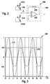
- FIG. 15 shows a diagram 300 which shows a relationship between a harmonic deflection 310 (broken line) of the gate electrode G of the measuring element 100 from the FIGS. 1a, 1b and an output signal 320 (solid line) of the signal processing means 220 Fig. 2 represents.
- a harmonic deflection 310 broken line
- an output signal 320 solid line
- the horizontal direction is a time course, in the vertical direction, a percentage deflection (with respect to 310) or a voltage (with respect to 320) plotted.
- the profile 310 of a sinusoidal, harmonic excursion of G causes an output voltage 320 corresponding to a symmetrical sawtooth or a trapezoid.
- This relationship stems from the particular shape of area 120 as a clipped circle or clipped ellipse, as in FIG Fig. 1b shown and described in more detail above.
- the sinusoidal, harmonic deflection 310 can be transmitted to the gate electrode G by a micromechanically structured actuator.
- a micromechanically structured actuator For example, by means of the measuring element 100 Fig. 1 with the help of a capacitive, piezoelectric, thermoelastic or magnetic drive a micro-electromechanical resonator can be constructed. According to its use, the resonator may be more or less damped, for example by gas confinement in a space in which the gate electrode G is deflectably arranged.
- the actuator and the in Fig. 2 Elements shown can form a micro-electro-mechanical signal generator that can be used in many ways. With such a signal generator, by varying the shapes of the gate electrode G and / or the region 120, a series of differently shaped periodic signals can be generated.
- the sensing element 100 can be used widely within micro-electro-mechanical and opto-micro-electro-mechanical devices.
- it may form a measuring device 200 together with further measuring elements 100, 210 and / or a device 220 for signal processing.
- a non-linearity of the signal processing device (and / or another signal processing device) can thus be compensated by the nonlinearity of the relationship between the deflection of the gate electrode G of the measuring element 100 and the current flow through the measuring element 100, so that overall There is an association between the deflection of the gate electrode G with respect to the region 120 and the output signal of the signal processing device.
- the measuring element 100 or the measuring device 200 may form a system or an assembly together with other mechanical, optical and / or electronic components.
- the measuring element 100 may be part of an initial sensor, a rotation rate sensor or a micromirror. In the latter case, there would be an opto-mechanical micro-electro-mechanical system (Micro-Opto-Mechanical System, MOEMS).
- MOEMS opto-mechanical micro-electro-mechanical system
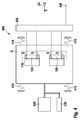
- FIG. 4 shows a resonator 400 in a FIGS. 1 a and 1 b corresponding representation.
- the resonator 400 comprises a substrate 110 with a plurality of source terminals S and drain terminals D, which delimit pairwise channels 120, a common electrode G, a processing device 220, springs 410, a drive 420, a damper 430 and an output 440th
- the processing device 220 is connected to the source terminals S and the drain terminals D and determines an output signal according to the above explanations, which provides them at the output 440.
- the electrode G is arranged in the z-direction over the channels 120 by means of the springs 410 and can be deflected by the drive 420 in the y-direction.
- the electrode G has recesses, so that the channels 120 more or less overlap with these depending on a deflection of the electrode G. Due to the overlapping of the electrode G with a plurality of channels 120, an increased sensitivity of the deflection measurement can be achieved in the illustrated resonator 400.
- At least one of the springs 410 serves at the same time as an electrical contact to an anchor element, not shown, for the resonator 400, which may carry, for example, the substrate 110 or may coincide therewith.
- the deflection of the electrode G is damped by means of the damper 430.
- This may be e.g. to act a friction or eddy current damper or the electrode G may be enclosed in a container with a gas of a predetermined pressure.
- the latter variant is particularly suitable for low attenuation in order to operate the resonator 400 at a high quality.
- the damping can also be effected by fluidic effects on the remaining movable structure and by "anchor loss".
- the damper 430 is omitted.
- the electrode G may be part of or associated with a micromirror.
- a micromirror system for example, an actual deflection of the electrode G can be determined on the basis of the signal provided at the output 440 and the drive 420 can be controlled accordingly in order to achieve a predetermined deflection of the electrode G.
- the electrode G may be part of an inertial system. The deflection of the electrode G can then be determined absolutely or as a function of a deflection of the electrode G induced by the drive 420, which allows conclusions to be drawn on a movement of the inertial system.
Landscapes
- Engineering & Computer Science (AREA)
- Power Engineering (AREA)
- Physics & Mathematics (AREA)
- General Physics & Mathematics (AREA)
- Micromachines (AREA)
- Junction Field-Effect Transistors (AREA)
- Particle Formation And Scattering Control In Inkjet Printers (AREA)
- Peptides Or Proteins (AREA)
Description
Die Erfindung betrifft ein Messelement. Insbesondere betrifft die Erfindung ein mikromechanisches Messelement mit einem elektrischem Ausgangssignal.The invention relates to a measuring element. In particular, the invention relates to a micromechanical measuring element with an electrical output signal.
Mikromechanische Messelemente werden in Sensoren für verschiedenste Anwendungsbereiche eingesetzt. Beispielsweise können Beschleunigungs-, Drehraten- oder Drucksensoren mikromechanisch aufgebaut werden. Dabei umfasst ein solches Messelement sowohl mechanische als auch elektrische Strukturen, die eine ähnliche Größenordnung aufweisen können und miteinander ein integriertes, mikro-elektromechanisches System bilden (Micro-Electro-Mechanical System, MEMS). Gelegentlich umfassen solche mikro-elektromechanischen Systeme auch einen Aktuator für Teile der mechanischen Strukturen, beispielsweise in Drehratensensoren, in denen eine auf eine bewegte Masse wirkende Kraft bestimmt werden soll. Auch ein mikro-elektromechanischer Resonator kann einen solchen Antrieb umfassen.Micromechanical measuring elements are used in sensors for a wide variety of applications. For example, acceleration, rotation rate or pressure sensors can be micromechanically constructed. In this case, such a measuring element comprises both mechanical and electrical structures, which may have a similar magnitude and together form an integrated, micro-electro-mechanical system (micro-electro-mechanical system, MEMS). Occasionally, such micro-electro-mechanical systems also include an actuator for parts of the mechanical structures, for example in yaw rate sensors, in which a force acting on a moving mass is to be determined. A micro-electromechanical resonator may also include such a drive.
In einer Form mikro-elektromechanischer Messelemente wird eine relative Auslenkung zwischen mechanischen Elementen ausgewertet, indem wenigstens eines der mechanischen Elemente zugleich auch Teil eines elektronischen Elements ist, welches ein mit der mechanischen Auslenkung korrelierendes Ausgangssignal bereitstellt. Eine solche Auslenkung kann in der Größenordnung der Strukturen, aus denen das Messelement aufgebaut ist, liegen. Die Auslenkung kann z. B. bestimmt werden, indem eine auslenkungsabhängige Kapazität bestimmt wird.In a form of micro-electromechanical measuring elements, a relative deflection between mechanical elements is evaluated by at least one of the mechanical elements being at the same time also part of an electronic element which provides an output signal correlating with the mechanical deflection. Such a deflection can be on the order of the structures of which the measuring element is constructed. The deflection can z. B. determined by a deflection-dependent capacity is determined.
Beispielsweise kann bei der "Moving Gate" - Technik eine flächige Gate-Elektrode eines Feldeffekttransistors (FET) parallel zu einem Kanal des FET angebracht und relativ zum Kanal ausgelenkt werden. Der Kanal wird durch einen Source- und einen Drainanschluss des Feldeffekttransistors begrenzt. Dabei wird zwischen dem Source- und dem Drainanschluss eine Spannung angelegt und die Gate-Elektrode elektrisch mit dem Drainanschluss verbunden, so dass der Feldeffekttransistor als Stromsteuerung betrieben wird. Ein Stromfluss durch den Feldeffekttransistor ändert sich dann in Abhängigkeit des elektrischen Feldes, welches sich auf Grund der Spannung zwischen der Gate-Elektrode und dem Kanal einstellt. Ändert sich die Anordnung von Gate-Elektrode und Kanal, so ändert sich letztlich auch der Stromfluss durch den Feldeffekttransistor. Die kapazitive Messung bietet sich für MEMS-Messaufnehmer an, da hier praktisch keine Rückwirkung von dem (auslenkungsabhängigen) Stromfluss auf die Auslenkung der Elektrode stattfindet. Gewöhnlich sind die Gate-Elektrode und der Kanal jeweils so geformt, dass ein Bereich, in dem sich die beiden überlappen, zu einer Auslenkung der Gate-Elektrode linear veränderlich ist. Durch die Auslenkung verändert sich die Größe des überlappenden Bereichs, so dass sich das elektrische Feld zwischen Gate-Elektrode und Kanale verändert, welches den Stromfluss durch den Feldeffekttransistor steuert. Somit kann die Auslenkung der Gate-Elektrode anhand des Stromflusses durch den Feldeffekttransistor bestimmt werden.For example, in the "moving gate" technique, a planar gate electrode of a field effect transistor (FET) may be mounted in parallel with a channel of the FET and deflected relative to the channel. The channel is limited by a source and a drain terminal of the field effect transistor. In this case, a voltage is applied between the source and the drain terminal and the gate electrode is electrically connected to the drain terminal, so that the field effect transistor is operated as current control. A current flow through the field effect transistor then changes as a function of the electric field, which is established on the basis of the voltage between the gate electrode and the channel. If the arrangement of the gate electrode and the channel changes, the current flow through the field effect transistor ultimately also changes. The capacitive measurement is suitable for MEMS sensors as there is virtually no reaction from the (deflection-dependent) current flow to the deflection of the electrode. Usually, the gate electrode and the channel are each shaped such that a region where the two overlap is linearly variable with respect to a deflection of the gate electrode. As a result of the deflection, the size of the overlapping region changes, so that the electric field between the gate electrode and the channel changes, which controls the current flow through the field effect transistor. Thus, the deflection of the gate electrode can be determined based on the current flow through the field effect transistor.
Das
Messsysteme, die ein Sensorsignal verarbeiten, sollen üblicherweise ein Ausgangssignal bereitstellen, das in einem möglichst linearen Zusammenhang mit einer zu messenden Größe stehen. Aus diesem Grund werden gewöhnlich alle Elemente des Systems mit linearen Kennlinien ausgelegt, so dass sich über das gesamte System der geforderte lineare Zusammenhang einstellt. Insbesondere bei komplexen, zahlreiche verarbeitende Elemente umfassenden Systemen ist es jedoch schwierig, die Linearität jedes einzelnen Elements in erforderlicher Qualität sicher zu stellen. Der Erfindung liegt daher die Aufgabe zu Grunde, einen MEMS-Sensor bereitzustellen, mit Hilfe dessen eine Erfassung und Auswertung einer Auslenkung verbessert werden kann.Measuring systems which process a sensor signal are usually intended to provide an output signal which is as linear as possible in relation to a quantity to be measured. For this reason, all elements of the system are usually designed with linear characteristics, so that sets the required linear relationship over the entire system. However, especially with complex systems comprising numerous processing elements, it is difficult to ensure the linearity of each element in required quality. The invention is therefore based on the object To provide a MEMS sensor, by means of which a detection and evaluation of a deflection can be improved.
Aus der Schrift
Aus der Schrift
Aus der Schrift
Diese Aufgabe wird gelöst durch ein Messelement nach Anspruch 1. Ansprüche 8 und 9 geben Messeinrichtungen an, die auf einem solchen Messelement basieren. Anspruch 11 definiert einen Resonator, der auf einer dieser Messeinrichtungen basiert. Unteransprüche geben weitere Ausgestaltungen bzw. Merkmale wieder.This object is achieved by a measuring element according to claim 1.
Die Erfindung geht von einem auf einem Feldeffekttransistor basierenden Messelement aus. Das Messelement umfasst einen auf einem Halbleitersubstrat angeordneten Bereich (beispielsweise ein Kanal eines Feldeffekttransistors) und eine Elektrode, mittels derer die Leitfähigkeit des Bereichs beeinflussbar ist. Der Überlappungsbereich zwischen der Gate-Elektrode und dem Bereich weist eine Breite (parallel zur Auslenkungsrichtung) und eine Länge (senkrecht zur Auslenkungsrichtung) auf. Eine Ausdehnung (Fläche) des Überlappungsbereichs ist von der Auslenkung und von den Formen der überlappenden Elemente abhängig. Es wird vorgeschlagen, die Gate-Elektrode und/oder den Bereich derart zu formen, dass die Ausdehnung des überlappenden Bereichs in einem nichtlinearen Zusammenhang mit der Auslenkung der Gate-Elektrode steht. Dies kann dadurch bewirkt werden, dass die Gate-Elektrode und/oder der Bereich eine von einem Rechteck verschiedene Form aufweist.The invention is based on a measuring element based on a field effect transistor. The measuring element comprises a region arranged on a semiconductor substrate (for example a channel of a field-effect transistor) and an electrode by means of which the conductivity of the region can be influenced. The overlapping area between the gate electrode and the area has a width (parallel to the deflection direction) and a length (perpendicular to the deflection direction). An extent (area) of the overlap area depends on the deflection and the shapes of the overlapping elements. It is proposed to form the gate electrode and / or the region in such a way that the extent of the overlapping region is in a non-linear relationship with the deflection of the gate electrode. This can be effected by the gate electrode and / or the region having a shape different from a rectangle.
In einer Ausführungsform kann beispielsweise die Gate-Elektrode eine konventionell rechteckige Form mit parallel bzw. senkrecht zur Auslenkungsrichtung verlaufenden Kanten aufweisen, während der Bereich eine von einem Rechteck verschiedene Form aufweist. Soll das Ausgangssignal symmetrisch zu einem einer Auslenkung von 0 entsprechenden Wert verlaufen, so ist bei rechteckiger Gate-Elektrode der Bereich in positiver Auslenkungsrichtung spiegelbildlich ebenso auszuformen wie in negativer Auslenkungsrichtung. Die Form des Bereichs ist also symmetrisch zu einer senkrecht zur Auslenkungsrichtung und durch eine Auslenkung von 0 verlaufenden Symmetrieachse. In alternativen Ausführungsformen können sowohl die Gate-Elektrode als auch der Bereich auch andere Formen annehmen, insbesondere können die Formen von Bereich und Gate-Elektrode auch vertauscht werden oder sowohl Bereich als auch Gate-Elektrode eine von einem Rechteck verschiedene Form aufweisen. Die Abweichungen von einer konventionellen Form eines Parallelogramms oder eines Rechtecks können größer als fertigungstechnisch bedingt und insbesondere größer als ca. 3-5% sein.For example, in one embodiment, the gate electrode may have a conventionally rectangular shape with edges parallel to or perpendicular to the direction of deflection, while the area may have a different shape than a rectangle. If the output signal is to run symmetrically to a value corresponding to a deflection of 0, then in the case of a rectangular gate electrode, the region in the positive deflection direction is to be mirror-inverted as well as in the negative deflection direction. The shape of the region is thus symmetrical to a symmetry axis extending perpendicular to the deflection direction and by a deflection of 0. In alternative embodiments, both the gate electrode and the region may be others In particular, the shapes of region and gate electrode can also be reversed, or both the region and the gate electrode can have a different shape than a rectangle. The deviations from a conventional form of a parallelogram or a rectangle may be greater than production-related and in particular greater than about 3-5%.
In einer Ausführungsform ist die Gate-Elektrode rechteckig und der Bereich weist eine Form auf, die einem Kreis entspricht, von dem ein oberer und ein unterer Bereich entlang zweier senkrecht zur Bewegungsrichtung der Gate-Elektrode verlaufender Trennlinien entfernt wurden. Diese Ausführungsform eignet sich insbesondere zum Einsatz in einem mikro-elektromechanischen Resonator.In one embodiment, the gate electrode is rectangular and the region has a shape corresponding to a circle from which an upper and a lower region have been removed along two separating lines perpendicular to the direction of movement of the gate electrode. This embodiment is particularly suitable for use in a micro-electromechanical resonator.
Die Erfindung wird nun mit Bezug auf die beigefügten Zeichnungen näher beschrieben, wobei
-
Fign. 1 a und 1 b unterschiedliche Ansichten eines Messelements auf der Basis eines MG-FETs; -
Fig. 2 eine Messvorrichtung auf der Basis des Messelements ausFig. 1 ; -
Fig. 3 einDiagramm 300 zeigt, welches die Auswirkung der Geometrie desBereichs 120 ausFig. 1 in der Messvorrichtung ausFig. 2 , und -
Fig. 4 einen Resonator auf der Basis des Messelements ausFig. 1 darstellt.
-
FIGS. 1 a and 1b different views of a measuring element based on a MG-FETs; -
Fig. 2 a measuring device based on the measuring elementFig. 1 ; -
Fig. 3 a diagram 300 showing the effect of the geometry ofregion 120 is shownFig. 1 in the measuring deviceFig. 2 , and -
Fig. 4 a resonator on the basis of the measuring elementFig. 1 represents.
Gleiche bzw. einander entsprechende Elemente tragen in allen Figuren gleiche Bezugszeichen.Identical or corresponding elements carry the same reference numerals in all figures.
Ein Messelement 100 umfasst ein Halbleitersubstrat 110, auf dem ein Sourceanschluss S und ein Drainanschluss D angebracht sind, zwischen denen sich ein Bereich 120 erstreckt. Das Messelement 100 umfasst außerdem eine oberhalb (in positiver z-Richtung) des Bereichs 120 angebrachte Gate-Elektrode G. Die Gate-Elektrode G ist in positiver und negativer y-Richtung auslenkbar angeordnet. Dabei bleibt ein Abstand zwischen der Gate-Elektrode G und dem Bereich 120 konstant, die Auslenkung findet nur entlang der y-Achse statt.A measuring
Nicht dargestellt ist eine elastische Anordnung, welche die Gate-Elektrode in einem vorbestimmten Abstand auslenkbar über dem Bereich 120 hält und Rückstellkräfte bewirkt, die mit der Auslenkung der Gate-Elektrode G in positiver und negativer y-Richtung veränderlich sind. Die elastische Verbindung kann beispielsweise mikromechanische Federn umfassen. In einem Punkt eines Gleichgewichts der Rückstellkräfte der elastischen Verbindung in positiver und negativer y-Richtung befindet sich eine unausgelenkte Position der Gate-Elektrode. In
Ebenfalls nicht dargestellt ist eine elektrische Verbindung der Gate-Elektrode G mit dem Drainanschluss D, die beispielsweise die elastische Anordnung umfassen kann. Durch die elektrische Verbindung wird das Messelement 100 stromsteuernd betrieben.Also not shown is an electrical connection of the gate electrode G to the drain terminal D, which may include, for example, the elastic assembly. Due to the electrical connection, the measuring
Wird eine Spannung zwischen der Gate-Elektrode G und Sourceanschluss S angelegt, so ermöglicht ein dadurch hervorgerufenes elektrisches Feld im Bereich 120 ein Bewegen von Ladungsträgern zwischen dem Sourceanschluss S und dem Drainanschluss D. Sind die Spannung zwischen der Gate-Elektrode G und dem Sourceanschluss S sowie der vertikale Abstand zwischen der Gate-Elektrode G und dem Bereich 120 konstant, so ist eine Beweglichkeit von Ladungsträgern im Bereich des Bereichs 120 nur von einer Ausdehnung eines Überlappungsbereichs 130 zwischen der Gate-Elektrode G und dem Bereich 120 abhängig. Ein Ausgangssignal der gezeigten Anordnung bestimmt sich grundsätzlich nach IDS∼W/L.When a voltage is applied between the gate electrode G and the source terminal S, an electric field caused thereby in the
Aus der in
Die Ausdehnung des Überlappungsbereichs 130 ergibt sich aus seiner Breite W, die proportional zur Auslenkung der Gate-Elektrode G ist, und der Länge L in dessen Verlauf über den Überlappungsbereich 130 (
Im vorliegenden Beispiel (s. ![]()
![]()
![]()
![]()
![]()
![]()
In weiteren Ausführungsformen kann die Gate-Elektrode auch andere Formen annehmen. Auch ist beispielsweise eine Begrenzung, Verschiebung oder Erweiterung der Auslenkung der Gate-Elektrode G bezüglich des Überlappungsbereichs 130 möglich. Ferner kann die Gate-Elektrode G beispielsweise perforiert sein. Das Messelement 100 kann auch einen weiteren Bereich (nicht dargestellt) aufweisen, der eine Leitfähigkeit einer weiteren Anordnung steuert undebenfalls von der Gate-Elektrode G überstrichen wird. Der weitere Bereich kann mit Bezug auf
Die Gate-Elektrode G kann auch Teil einer komplexeren mikro-elektromechanischen Anordnung mit mehreren beweglichen Elementen sein. Die Gate-Elektrode G kann mittels einer elastischen Anordnung an einem oder mehreren dieser Elemente und/oder am Halbleitersubstrat 110 befestigt sein, und die beweglichen Elemente können Federn umfassen.The gate electrode G may also be part of a more complex micro-electromechanical arrangement with a plurality of movable elements. The gate electrode G may be attached to one or more of these elements and / or to the
Das Messelement 210 ist grundsätzlich identisch zum Messelement 100 aufgebaut und weist insbesondere identische Abmessungen auf, umfasst jedoch im Gegensatz zum Messelement 100 keine beweglichen Teile. Eine Gate-Elektrode des Messelements 210 ist in einer Position fixiert, die an der Messeinrichtung 100 einer unausgelenkten Position von dessen Gate-Elektrode G entspricht. Bei beiden Messelementen 100 und 210 sind die Gate-Elektroden mit den jeweiligen Drainanschlüssen D verbunden, so dass beide Messelemente 100 und 210 stromsteuernd betrieben werden. Die Messelemente 100 und 210 sind in Serie geschaltet und mit zwei Anschlüssen VCC und GND einer Gleichspannungsquelle (nicht dargestellt) verbunden. Die Messelemente 100 und 210 sind bipolar, daher ist eine Polung der Gleichspannung ohne Belang. An einem Abgriff A zwischen den beiden Messelementen 100 und 210 ist ein Ausgangssignal abgreifbar, welches zur Auslenkung der Gate-Elektrode G im Messelement 100 in einem nichtlinearen Zusammenhang steht.The measuring
Durch die Kombination der Messelemente 100 und 210 in der gezeigten Weise werden konstante Fehler, die beispielsweise auf Fertigungsungenauigkeiten der Messelemente 100 und 210 zurückzuführen sind, kompensiert. Die Einrichtung 220 zur Signalverarbeitung erzeugt auf eine dem Fachmann bekannte Weise durch einen mittels des Rückkopplungswiderstands 230 rückgekoppelten Operationsverstärkers 225 aus dem am Abgriff A anliegenden Signal ein mit der Auslenkung der Gate-Elektrode G des Messelements 100 veränderliches Spannungssignal.The combination of the measuring
Es ist zu sehen, dass der Verlauf 310 einer sinusförmigen, harmonischen Auslenkung von G eine Ausgangsspannung 320 bewirkt, die einem symmetrischen Sägezahn bzw. einem Trapez entspricht. Dieser Zusammenhang rührt von der besonderen Form des Bereichs 120 als gekappter Kreis oder gekappte Ellipse, wie in
Die sinusförmige, harmonischen Auslenkung 310 kann von einem mikromechanisch aufgebauten Aktuator auf die Gate-Elektrode G übertragen werden. Beispielsweise kann mittels des Messelements 100 aus
Der Aktuator und die in
Das Messelement 100 kann vielseitig innerhalb von mikro-elektromechanischen und opto-mikro-elektromechanischen Bauelementen verwendet werden. Insbesondere kann es zusammen mit weiteren Messelementen 100, 210 und/oder einer Einrichtung 220 zur Signalverarbeitung eine Messeinrichtung 200 bilden. Eine Nichtlinearität der Einrichtung 220 zur Signalverarbeitung (und/oder einer anderen Einrichtung zur Signalverarbeitung) kann somit durch die Nichtlinearität des Zusammenhangs zwischen der Auslenkung der Gate-Elektrode G des Messelements 100 und dem Stromfluss durch das Messelement 100 kompensiert werden, so dass insgesamt ein linearer Zusammenhang zwischen der Auslenkung der Gate-Elektrode G gegenüber dem Bereich 120 und dem Ausgangssignal der Einrichtung zur Signalverarbeitung besteht.The
Das Messelement 100 bzw. die Messeinrichtung 200 kann zusammen mit anderen mechanischen, optischen und/oder elektronischen Komponenten ein System oder eine Baugruppe bilden. Beispielsweise kann das Messelement 100 Teil eines Initialsensors, eines Drehratensensors oder eines Mikrospiegels sein. In letzterem Fall läge ein opto-mechanisches mikro-elektromechanisches System (Micro-Opto-Mechanical System, MOEMS) vor.The measuring
Die Verarbeitungseinrichtung 220 ist mit den Sourceanschlüssen S und den Drainanschlüssen D verbunden und bestimmt entsprechend obigen Erläuterungen ein Ausgangssignal, das sie am Ausgang 440 bereitstellt. Die Elektrode G ist mittels der Federn 410 in z-Richtung über den Kanälen 120 angeordnet und kann von dem Antrieb 420 in y-Richtung ausgelenkt werden. Die Elektrode G weist Aussparungen auf, so dass die Kanäle 120 in Abhängigkeit einer Auslenkung der Elektrode G mehr oder minder mit diesen überlappen. Durch die Überlappung der Elektrode G mit mehreren Kanälen 120 kann im dargestellten Resonator 400 eine erhöhte Empfindlichkeit der Auslenkungsmessung erzielt werden.The
Wenigstens eine der Federn 410 dient gleichzeitig als elektrischer Kontakt an ein nicht gezeigtes Ankerelement für den Resonator 400, das beispielsweise das Substrat 110 tragen oder mit diesem zusammenfallen kann. Die Auslenkung der Elektrode G wird mittels des Dämpfers 430 gedämpft. Dabei kann es sich z.B. um einen Reibungs- oder Wirbelstromdämpfer handeln oder die Elektrode G kann in einem Behältnis mit einem Gas eines vorbestimmten Drucks eingeschlossen sein. Letztere Variante eignet sich besonders für schwache Dämpfungen, um den Resonator 400 bei einer hohen Güte zu betreiben. Die Dämpfung kann auch durch fluidische Effekte an der verbleibenden beweglichen Struktur und durch Materialdämpfung ("anchor loss") bewirkt werden. Gegebenenfalls wird der Dämpfer 430 weggelassen.At least one of the
Die Elektrode G kann Teil eines Mikrospiegels oder mit einem solchen verbunden sein. In einem Mikrospiegel-System kann beispielsweise eine tatsächliche Auslenkung der Elektrode G anhand des am Ausgang 440 bereitgestellten Signals bestimmt und der Antrieb 420 entsprechend angesteuert werden, um eine vorbestimmte Auslenkung der Elektrode G zu erzielen. In einer weiteren Ausführungsform kann die Elektrode G Teil eines Inertialsystems sein. Die Auslenkung der Elektrode G kann dann absolut oder in Abhängigkeit einer durch den Antrieb 420 induzierten Auslenkung der Elektrode G bestimmt werden, was Rückschlüsse auf eine Bewegung des Inertialsystems zulässt.The electrode G may be part of or associated with a micromirror. In a micromirror system, for example, an actual deflection of the electrode G can be determined on the basis of the signal provided at the
Claims (13)
- Measuring element (100) designed to pick up a deflection, comprising the following:- a region (120) arranged on a semiconductor substrate (110), said region extending between a source terminal (S) and a drain terminal (D), and an electrode (G) designed to influence the conductivity of the region (120);- wherein the electrode (G) is fitted in a deflectable fashion relative to the region (120) in such a way that an overlap region (130) results between the electrode (G) and the region (120), said overlap region having an extent that is variable with a deflection of the electrode (G), and- wherein the output signal of the measuring element (100) is dependent on the conductivity of the region (120) and is controllable by the change in the extent of the overlap region (130),- the region and/or the electrode are embodied in such a way that the change in the extent of the overlap region (130) is in a non-linear relationship with the deflection of the electrode (G), such that a change in the output signal of the measuring element (100) is in a non-linear relationship with the deflection of the electrode (G),wherein• the electrode (G) is fitted above the region (120), wherein the distance between the electrode (G) and the region (120) remains constant, and• a surface area of the region (120) is determined by a width W - running in a deflection direction y of the electrode (G) - and a length L - running perpendicular thereto - of the electrode (G), and the following holds true:

- Measuring element (100) according to Claim 1, characterized in that the electrode (G) and the region (120) are arranged such that they are spaced apart.
- Measuring element (100) according to Claim 1, wherein the length (L) of the region (120) does not run in a constant fashion over the width (W) of the region (120) .
- Measuring element (100) according to any of the preceding claims, wherein the drain terminal (D) and/or the source terminal (S) have/has an edge line of the region (120) in the form of an ellipse segment.
- Measuring element (100) according to Claim 1, characterized in that the region (120) has a variable length L between the drain terminal (D) and the source terminal (S), wherein the following holds true for the length L as a function of the deflection direction y of the electrode (G) :

- Measuring element (100) according to any of Claims 1 to 5, wherein the region (120) is the channel of a field effect transistor and is at least partly swept over by the electrode (G) during the deflection thereof.
- Measuring element (100) according to any of Claims 1 to 6, wherein the electrode (G) is perforated.
- Measuring element (100) according to any of Claims 1 to 7, wherein the electrode (G) is part of a micromirror or of an inertial sensor.
- Measuring element (100) according to any of Claims 1 to 8, furthermore comprising an elastic element (410), by means of which the electrode (G) is fitted to the semiconductor substrate (110) in a deflectable fashion.
- Measuring element (100) according to any of Claims 1 to 9, wherein an electrode (G) is assigned to a plurality of channels (120).
- Resonator (400), comprising
a measuring element (100) designed to pick up a deflection according to any of Claims 1 to 10, and a drive (420), wherein the measuring element comprises:- a region (120) arranged on a semiconductor substrate (110), said region extending between a source terminal (S) and a drain terminal (D), and an electrode (G) designed to influence the conductivity of the region (120);- wherein the electrode (G) is fitted in a deflectable fashion relative to the region (120) in such a way that an overlap region (130) results between the electrode (G) and the region (120), said overlap region having an extent that is variable with a deflection of the electrode (G), and- wherein the output signal of the measuring element (100) is dependent on the conductivity of the region (120) and is controllable by the change in the extent of the overlap region (130),- the region and/or the electrode are embodied in such a way that the change in the extent of the overlap region (130) is in a non-linear relationship with the deflection of the electrode (G), such that a change in the output signal of the measuring element (100) is in a non-linear relationship with the deflection of the electrode (G),wherein• the electrode (G) is fitted above the region (120), wherein the distance between the electrode (G) and the region (120) remains constant, and• a surface area of the region (120) is determined by a width W - running in a deflection direction y of the electrode (G) - and a length L - running perpendicular thereto - of the electrode (G), and the following holds true: • wherein the drive (420) periodically deflects the electrode (G).
 - Resonator (400) according to Claim 11, characterized in that at least two measuring elements (100) are provided, wherein the measuring elements (100) have a common semiconductor substrate (110) with a plurality of source terminals (S) and drain terminals (D), which delimit regions (120) in pairs, and a common electrode (G), wherein a processing unit (220) is provided, which is connected to the source terminals (S) and the drain terminals (D) and provides an output signal depending on the deflection of the electrode (G) in the form of a non-linear relationship.
- Resonator according to Claim 12, characterized in that the drive (420) transmits a sinusoidal, harmonic deflection (310) to the electrode (G), wherein the processing unit (220) brings about, depending on said sinusoidal deflection (310), an output voltage (320) corresponding to a symmetrical sawtooth or a trapezium.
Applications Claiming Priority (2)
| Application Number | Priority Date | Filing Date | Title |
|---|---|---|---|
| DE102009002723A DE102009002723A1 (en) | 2009-04-29 | 2009-04-29 | measuring element |
| PCT/EP2010/052527 WO2010124889A2 (en) | 2009-04-29 | 2010-03-01 | Measuring element |
Publications (2)
| Publication Number | Publication Date |
|---|---|
| EP2425208A2 EP2425208A2 (en) | 2012-03-07 |
| EP2425208B1 true EP2425208B1 (en) | 2016-05-11 |
Family
ID=42813536
Family Applications (1)
| Application Number | Title | Priority Date | Filing Date |
|---|---|---|---|
| EP10708754.6A Not-in-force EP2425208B1 (en) | 2009-04-29 | 2010-03-01 | Measuring element |
Country Status (4)
| Country | Link |
|---|---|
| US (1) | US9086302B2 (en) |
| EP (1) | EP2425208B1 (en) |
| DE (1) | DE102009002723A1 (en) |
| WO (1) | WO2010124889A2 (en) |
Families Citing this family (4)
| Publication number | Priority date | Publication date | Assignee | Title |
|---|---|---|---|---|
| DE102009045422B4 (en) | 2009-10-07 | 2024-05-02 | Robert Bosch Gmbh | Sensor arrangement and method for operating a sensor arrangement |
| DE102011075541A1 (en) | 2011-05-10 | 2012-11-15 | Robert Bosch Gmbh | Evaluation circuit for field effect transistor with movable gate structure |
| DE102012202783A1 (en) * | 2012-02-23 | 2013-08-29 | Robert Bosch Gmbh | Micromechanical sensor device with movable gate and corresponding manufacturing method |
| JP7410935B2 (en) | 2018-05-24 | 2024-01-10 | ザ リサーチ ファウンデーション フォー ザ ステイト ユニバーシティー オブ ニューヨーク | capacitive sensor |
Citations (2)
| Publication number | Priority date | Publication date | Assignee | Title |
|---|---|---|---|---|
| EP0693672A1 (en) * | 1994-07-01 | 1996-01-24 | Dr. Johannes Heidenhain GmbH | Length or angle measuring device |
| WO2005080921A1 (en) * | 2004-02-19 | 2005-09-01 | Eaton Automotive B.V. | Mechatronic control system |
Family Cites Families (5)
| Publication number | Priority date | Publication date | Assignee | Title |
|---|---|---|---|---|
| US4157462A (en) * | 1977-10-26 | 1979-06-05 | General Motors Corporation | Sensor |
| US5457368A (en) * | 1993-03-09 | 1995-10-10 | University Of Utah Research Foundation | Mechanical/electrical displacement transducer |
| US5198740A (en) * | 1989-10-04 | 1993-03-30 | University Of Utah Research Foundation | Sliding contact mechanical/electrical displacement transducer |
| EP0700065B1 (en) * | 1994-08-31 | 2001-09-19 | AT&T Corp. | Field emission device and method for making same |
| US6220096B1 (en) | 1997-03-20 | 2001-04-24 | Interscience, Inc. | Differential wideband vibration |
-
2009
- 2009-04-29 DE DE102009002723A patent/DE102009002723A1/en not_active Withdrawn
-
2010
- 2010-03-01 EP EP10708754.6A patent/EP2425208B1/en not_active Not-in-force
- 2010-03-01 WO PCT/EP2010/052527 patent/WO2010124889A2/en not_active Ceased
- 2010-03-01 US US13/258,570 patent/US9086302B2/en active Active
Patent Citations (2)
| Publication number | Priority date | Publication date | Assignee | Title |
|---|---|---|---|---|
| EP0693672A1 (en) * | 1994-07-01 | 1996-01-24 | Dr. Johannes Heidenhain GmbH | Length or angle measuring device |
| WO2005080921A1 (en) * | 2004-02-19 | 2005-09-01 | Eaton Automotive B.V. | Mechatronic control system |
Also Published As
| Publication number | Publication date |
|---|---|
| WO2010124889A3 (en) | 2011-01-13 |
| DE102009002723A1 (en) | 2010-11-04 |
| US9086302B2 (en) | 2015-07-21 |
| EP2425208A2 (en) | 2012-03-07 |
| WO2010124889A2 (en) | 2010-11-04 |
| WO2010124889A4 (en) | 2011-04-14 |
| US20120025277A1 (en) | 2012-02-02 |
Similar Documents
| Publication | Publication Date | Title |
|---|---|---|
| EP2389561B1 (en) | Yaw rate sensor | |
| EP1373831B1 (en) | Angular rate sensor | |
| EP1377797B1 (en) | Rotation rate sensor | |
| DE102012200929B4 (en) | Micromechanical structure and method for manufacturing a micromechanical structure | |
| WO2008074538A1 (en) | Acceleration sensor with comb-shaped electrodes | |
| DE4432837A1 (en) | Capacitive acceleration sensor and measurement method esp. using seismic mass and surface micro-mechanic electrodes | |
| DE102009000606A1 (en) | Micromechanical structures | |
| DE102008040855A1 (en) | Three-axis accelerometer | |
| DE112013002514T5 (en) | sensor device | |
| EP2425208B1 (en) | Measuring element | |
| DE102013212059B4 (en) | Micromechanical inertial sensor | |
| DE102009045420B4 (en) | Rotation rate sensor, rotation rate sensor arrangement and method for operating a rotation rate sensor | |
| DE102008054749A1 (en) | Rotation rate sensor and method for operating a rotation rate sensor | |
| DE102013216935A1 (en) | Rotation rate sensor with pre-set quadrature offset | |
| DE102009028343A1 (en) | Sensor element and method for operating a sensor element | |
| DE102008040567B4 (en) | Method for operating a sensor module and a sensor module | |
| DE112006003699B4 (en) | Deflectible micromechanical system and its use | |
| DE19744292A1 (en) | Rotation rate sensor with decoupled orthogonal primary and secondary oscillators, esp. of Coriolis micro-mechanical type | |
| EP1608988B1 (en) | Acceleration sensor and method for detecting an acceleration | |
| DE102020210121A1 (en) | Micromechanical system, method for operating a micromechanical system | |
| DE102010038919B4 (en) | Micromechanical system | |
| DE19813941A1 (en) | Micromechanical acceleration sensor | |
| DE4431232A1 (en) | Integratable spring-mass system for micro-mechanical e.g. acceleration sensor | |
| DE102011080982B4 (en) | Sensor arrangement | |
| DE102010039236B4 (en) | Sensor arrangement and method for adjusting a sensor arrangement |
Legal Events
| Date | Code | Title | Description |
|---|---|---|---|
| PUAI | Public reference made under article 153(3) epc to a published international application that has entered the european phase |
Free format text: ORIGINAL CODE: 0009012 |
|
| 17P | Request for examination filed |
Effective date: 20111129 |
|
| AK | Designated contracting states |
Kind code of ref document: A2 Designated state(s): AT BE BG CH CY CZ DE DK EE ES FI FR GB GR HR HU IE IS IT LI LT LU LV MC MK MT NL NO PL PT RO SE SI SK SM TR |
|
| DAX | Request for extension of the european patent (deleted) | ||
| 17Q | First examination report despatched |
Effective date: 20150511 |
|
| GRAP | Despatch of communication of intention to grant a patent |
Free format text: ORIGINAL CODE: EPIDOSNIGR1 |
|
| INTG | Intention to grant announced |
Effective date: 20151216 |
|
| GRAS | Grant fee paid |
Free format text: ORIGINAL CODE: EPIDOSNIGR3 |
|
| GRAA | (expected) grant |
Free format text: ORIGINAL CODE: 0009210 |
|
| AK | Designated contracting states |
Kind code of ref document: B1 Designated state(s): AT BE BG CH CY CZ DE DK EE ES FI FR GB GR HR HU IE IS IT LI LT LU LV MC MK MT NL NO PL PT RO SE SI SK SM TR |
|
| REG | Reference to a national code |
Ref country code: GB Ref legal event code: FG4D Free format text: NOT ENGLISH |
|
| REG | Reference to a national code |
Ref country code: CH Ref legal event code: EP |
|
| REG | Reference to a national code |
Ref country code: AT Ref legal event code: REF Ref document number: 799010 Country of ref document: AT Kind code of ref document: T Effective date: 20160515 |
|
| REG | Reference to a national code |
Ref country code: IE Ref legal event code: FG4D Free format text: LANGUAGE OF EP DOCUMENT: GERMAN |
|
| REG | Reference to a national code |
Ref country code: DE Ref legal event code: R096 Ref document number: 502010011649 Country of ref document: DE |
|
| REG | Reference to a national code |
Ref country code: LT Ref legal event code: MG4D |
|
| REG | Reference to a national code |
Ref country code: NL Ref legal event code: MP Effective date: 20160511 |
|
| PG25 | Lapsed in a contracting state [announced via postgrant information from national office to epo] |
Ref country code: NO Free format text: LAPSE BECAUSE OF FAILURE TO SUBMIT A TRANSLATION OF THE DESCRIPTION OR TO PAY THE FEE WITHIN THE PRESCRIBED TIME-LIMIT Effective date: 20160811 Ref country code: LT Free format text: LAPSE BECAUSE OF FAILURE TO SUBMIT A TRANSLATION OF THE DESCRIPTION OR TO PAY THE FEE WITHIN THE PRESCRIBED TIME-LIMIT Effective date: 20160511 Ref country code: FI Free format text: LAPSE BECAUSE OF FAILURE TO SUBMIT A TRANSLATION OF THE DESCRIPTION OR TO PAY THE FEE WITHIN THE PRESCRIBED TIME-LIMIT Effective date: 20160511 Ref country code: NL Free format text: LAPSE BECAUSE OF FAILURE TO SUBMIT A TRANSLATION OF THE DESCRIPTION OR TO PAY THE FEE WITHIN THE PRESCRIBED TIME-LIMIT Effective date: 20160511 |
|
| PG25 | Lapsed in a contracting state [announced via postgrant information from national office to epo] |
Ref country code: HR Free format text: LAPSE BECAUSE OF FAILURE TO SUBMIT A TRANSLATION OF THE DESCRIPTION OR TO PAY THE FEE WITHIN THE PRESCRIBED TIME-LIMIT Effective date: 20160511 Ref country code: GR Free format text: LAPSE BECAUSE OF FAILURE TO SUBMIT A TRANSLATION OF THE DESCRIPTION OR TO PAY THE FEE WITHIN THE PRESCRIBED TIME-LIMIT Effective date: 20160812 Ref country code: LV Free format text: LAPSE BECAUSE OF FAILURE TO SUBMIT A TRANSLATION OF THE DESCRIPTION OR TO PAY THE FEE WITHIN THE PRESCRIBED TIME-LIMIT Effective date: 20160511 Ref country code: SE Free format text: LAPSE BECAUSE OF FAILURE TO SUBMIT A TRANSLATION OF THE DESCRIPTION OR TO PAY THE FEE WITHIN THE PRESCRIBED TIME-LIMIT Effective date: 20160511 Ref country code: PT Free format text: LAPSE BECAUSE OF FAILURE TO SUBMIT A TRANSLATION OF THE DESCRIPTION OR TO PAY THE FEE WITHIN THE PRESCRIBED TIME-LIMIT Effective date: 20160912 Ref country code: ES Free format text: LAPSE BECAUSE OF FAILURE TO SUBMIT A TRANSLATION OF THE DESCRIPTION OR TO PAY THE FEE WITHIN THE PRESCRIBED TIME-LIMIT Effective date: 20160511 |
|
| PG25 | Lapsed in a contracting state [announced via postgrant information from national office to epo] |
Ref country code: RO Free format text: LAPSE BECAUSE OF FAILURE TO SUBMIT A TRANSLATION OF THE DESCRIPTION OR TO PAY THE FEE WITHIN THE PRESCRIBED TIME-LIMIT Effective date: 20160511 Ref country code: EE Free format text: LAPSE BECAUSE OF FAILURE TO SUBMIT A TRANSLATION OF THE DESCRIPTION OR TO PAY THE FEE WITHIN THE PRESCRIBED TIME-LIMIT Effective date: 20160511 Ref country code: SK Free format text: LAPSE BECAUSE OF FAILURE TO SUBMIT A TRANSLATION OF THE DESCRIPTION OR TO PAY THE FEE WITHIN THE PRESCRIBED TIME-LIMIT Effective date: 20160511 Ref country code: DK Free format text: LAPSE BECAUSE OF FAILURE TO SUBMIT A TRANSLATION OF THE DESCRIPTION OR TO PAY THE FEE WITHIN THE PRESCRIBED TIME-LIMIT Effective date: 20160511 Ref country code: CZ Free format text: LAPSE BECAUSE OF FAILURE TO SUBMIT A TRANSLATION OF THE DESCRIPTION OR TO PAY THE FEE WITHIN THE PRESCRIBED TIME-LIMIT Effective date: 20160511 |
|
| REG | Reference to a national code |
Ref country code: DE Ref legal event code: R097 Ref document number: 502010011649 Country of ref document: DE |
|
| PG25 | Lapsed in a contracting state [announced via postgrant information from national office to epo] |
Ref country code: SM Free format text: LAPSE BECAUSE OF FAILURE TO SUBMIT A TRANSLATION OF THE DESCRIPTION OR TO PAY THE FEE WITHIN THE PRESCRIBED TIME-LIMIT Effective date: 20160511 Ref country code: PL Free format text: LAPSE BECAUSE OF FAILURE TO SUBMIT A TRANSLATION OF THE DESCRIPTION OR TO PAY THE FEE WITHIN THE PRESCRIBED TIME-LIMIT Effective date: 20160511 |
|
| PLBE | No opposition filed within time limit |
Free format text: ORIGINAL CODE: 0009261 |
|
| STAA | Information on the status of an ep patent application or granted ep patent |
Free format text: STATUS: NO OPPOSITION FILED WITHIN TIME LIMIT |
|
| REG | Reference to a national code |
Ref country code: FR Ref legal event code: PLFP Year of fee payment: 8 |
|
| 26N | No opposition filed |
Effective date: 20170214 |
|
| PG25 | Lapsed in a contracting state [announced via postgrant information from national office to epo] |
Ref country code: SI Free format text: LAPSE BECAUSE OF FAILURE TO SUBMIT A TRANSLATION OF THE DESCRIPTION OR TO PAY THE FEE WITHIN THE PRESCRIBED TIME-LIMIT Effective date: 20160511 |
|
| REG | Reference to a national code |
Ref country code: CH Ref legal event code: PL |
|
| GBPC | Gb: european patent ceased through non-payment of renewal fee |
Effective date: 20170301 |
|
| PG25 | Lapsed in a contracting state [announced via postgrant information from national office to epo] |
Ref country code: MC Free format text: LAPSE BECAUSE OF FAILURE TO SUBMIT A TRANSLATION OF THE DESCRIPTION OR TO PAY THE FEE WITHIN THE PRESCRIBED TIME-LIMIT Effective date: 20160511 |
|
| REG | Reference to a national code |
Ref country code: IE Ref legal event code: MM4A |
|
| PG25 | Lapsed in a contracting state [announced via postgrant information from national office to epo] |
Ref country code: LU Free format text: LAPSE BECAUSE OF NON-PAYMENT OF DUE FEES Effective date: 20170301 |
|
| PG25 | Lapsed in a contracting state [announced via postgrant information from national office to epo] |
Ref country code: LI Free format text: LAPSE BECAUSE OF NON-PAYMENT OF DUE FEES Effective date: 20170331 Ref country code: GB Free format text: LAPSE BECAUSE OF NON-PAYMENT OF DUE FEES Effective date: 20170301 Ref country code: IE Free format text: LAPSE BECAUSE OF NON-PAYMENT OF DUE FEES Effective date: 20170301 Ref country code: CH Free format text: LAPSE BECAUSE OF NON-PAYMENT OF DUE FEES Effective date: 20170331 |
|
| REG | Reference to a national code |
Ref country code: BE Ref legal event code: MM Effective date: 20170331 |
|
| REG | Reference to a national code |
Ref country code: FR Ref legal event code: PLFP Year of fee payment: 9 |
|
| REG | Reference to a national code |
Ref country code: AT Ref legal event code: MM01 Ref document number: 799010 Country of ref document: AT Kind code of ref document: T Effective date: 20170301 |
|
| PG25 | Lapsed in a contracting state [announced via postgrant information from national office to epo] |
Ref country code: BE Free format text: LAPSE BECAUSE OF NON-PAYMENT OF DUE FEES Effective date: 20170331 |
|
| PG25 | Lapsed in a contracting state [announced via postgrant information from national office to epo] |
Ref country code: AT Free format text: LAPSE BECAUSE OF NON-PAYMENT OF DUE FEES Effective date: 20170301 |
|
| PG25 | Lapsed in a contracting state [announced via postgrant information from national office to epo] |
Ref country code: MT Free format text: LAPSE BECAUSE OF FAILURE TO SUBMIT A TRANSLATION OF THE DESCRIPTION OR TO PAY THE FEE WITHIN THE PRESCRIBED TIME-LIMIT Effective date: 20160511 |
|
| PG25 | Lapsed in a contracting state [announced via postgrant information from national office to epo] |
Ref country code: HU Free format text: LAPSE BECAUSE OF FAILURE TO SUBMIT A TRANSLATION OF THE DESCRIPTION OR TO PAY THE FEE WITHIN THE PRESCRIBED TIME-LIMIT; INVALID AB INITIO Effective date: 20100301 |
|
| PG25 | Lapsed in a contracting state [announced via postgrant information from national office to epo] |
Ref country code: BG Free format text: LAPSE BECAUSE OF FAILURE TO SUBMIT A TRANSLATION OF THE DESCRIPTION OR TO PAY THE FEE WITHIN THE PRESCRIBED TIME-LIMIT Effective date: 20160511 |
|
| PG25 | Lapsed in a contracting state [announced via postgrant information from national office to epo] |
Ref country code: CY Free format text: LAPSE BECAUSE OF NON-PAYMENT OF DUE FEES Effective date: 20160511 |
|
| PG25 | Lapsed in a contracting state [announced via postgrant information from national office to epo] |
Ref country code: MK Free format text: LAPSE BECAUSE OF FAILURE TO SUBMIT A TRANSLATION OF THE DESCRIPTION OR TO PAY THE FEE WITHIN THE PRESCRIBED TIME-LIMIT Effective date: 20160511 |
|
| PG25 | Lapsed in a contracting state [announced via postgrant information from national office to epo] |
Ref country code: TR Free format text: LAPSE BECAUSE OF FAILURE TO SUBMIT A TRANSLATION OF THE DESCRIPTION OR TO PAY THE FEE WITHIN THE PRESCRIBED TIME-LIMIT Effective date: 20160511 |
|
| PG25 | Lapsed in a contracting state [announced via postgrant information from national office to epo] |
Ref country code: IS Free format text: LAPSE BECAUSE OF FAILURE TO SUBMIT A TRANSLATION OF THE DESCRIPTION OR TO PAY THE FEE WITHIN THE PRESCRIBED TIME-LIMIT Effective date: 20160911 |
|
| PGFP | Annual fee paid to national office [announced via postgrant information from national office to epo] |
Ref country code: FR Payment date: 20220322 Year of fee payment: 13 |
|
| PGFP | Annual fee paid to national office [announced via postgrant information from national office to epo] |
Ref country code: IT Payment date: 20220331 Year of fee payment: 13 |
|
| PGFP | Annual fee paid to national office [announced via postgrant information from national office to epo] |
Ref country code: DE Payment date: 20230524 Year of fee payment: 14 |
|
| PG25 | Lapsed in a contracting state [announced via postgrant information from national office to epo] |
Ref country code: FR Free format text: LAPSE BECAUSE OF NON-PAYMENT OF DUE FEES Effective date: 20230331 |
|
| PG25 | Lapsed in a contracting state [announced via postgrant information from national office to epo] |
Ref country code: IT Free format text: LAPSE BECAUSE OF NON-PAYMENT OF DUE FEES Effective date: 20230301 |
|
| REG | Reference to a national code |
Ref country code: DE Ref legal event code: R119 Ref document number: 502010011649 Country of ref document: DE |
|
| PG25 | Lapsed in a contracting state [announced via postgrant information from national office to epo] |
Ref country code: DE Free format text: LAPSE BECAUSE OF NON-PAYMENT OF DUE FEES Effective date: 20241001 |
|
| PG25 | Lapsed in a contracting state [announced via postgrant information from national office to epo] |
Ref country code: DE Free format text: LAPSE BECAUSE OF NON-PAYMENT OF DUE FEES Effective date: 20241001 |