EP2423157A2 - MEMS pressure sensor device and method of fabricating same - Google Patents
MEMS pressure sensor device and method of fabricating same Download PDFInfo
- Publication number
- EP2423157A2 EP2423157A2 EP11176316A EP11176316A EP2423157A2 EP 2423157 A2 EP2423157 A2 EP 2423157A2 EP 11176316 A EP11176316 A EP 11176316A EP 11176316 A EP11176316 A EP 11176316A EP 2423157 A2 EP2423157 A2 EP 2423157A2
- Authority
- EP
- European Patent Office
- Prior art keywords
- substrate structure
- cavity
- sensor device
- reference element
- sense element
- Prior art date
- Legal status (The legal status is an assumption and is not a legal conclusion. Google has not performed a legal analysis and makes no representation as to the accuracy of the status listed.)
- Withdrawn
Links
- 238000004519 manufacturing process Methods 0.000 title abstract description 44
- 239000000758 substrate Substances 0.000 claims abstract description 103
- 238000000034 method Methods 0.000 claims abstract description 58
- 230000008878 coupling Effects 0.000 claims abstract description 8
- 238000010168 coupling process Methods 0.000 claims abstract description 8
- 238000005859 coupling reaction Methods 0.000 claims abstract description 8
- 230000004044 response Effects 0.000 claims abstract description 5
- 239000000463 material Substances 0.000 claims description 13
- 238000000151 deposition Methods 0.000 claims description 5
- 230000000694 effects Effects 0.000 description 36
- 230000008569 process Effects 0.000 description 30
- 238000012545 processing Methods 0.000 description 10
- 230000035945 sensitivity Effects 0.000 description 7
- 238000010348 incorporation Methods 0.000 description 6
- XUIMIQQOPSSXEZ-UHFFFAOYSA-N Silicon Chemical compound [Si] XUIMIQQOPSSXEZ-UHFFFAOYSA-N 0.000 description 5
- 239000003990 capacitor Substances 0.000 description 5
- 229910052710 silicon Inorganic materials 0.000 description 5
- 239000010703 silicon Substances 0.000 description 5
- KWYUFKZDYYNOTN-UHFFFAOYSA-M Potassium hydroxide Chemical compound [OH-].[K+] KWYUFKZDYYNOTN-UHFFFAOYSA-M 0.000 description 4
- 238000005530 etching Methods 0.000 description 4
- 238000013461 design Methods 0.000 description 3
- VYPSYNLAJGMNEJ-UHFFFAOYSA-N Silicium dioxide Chemical compound O=[Si]=O VYPSYNLAJGMNEJ-UHFFFAOYSA-N 0.000 description 2
- 230000015572 biosynthetic process Effects 0.000 description 2
- 230000008021 deposition Effects 0.000 description 2
- 238000005516 engineering process Methods 0.000 description 2
- 229910052751 metal Inorganic materials 0.000 description 2
- 239000002184 metal Substances 0.000 description 2
- 238000005459 micromachining Methods 0.000 description 2
- 238000000059 patterning Methods 0.000 description 2
- 239000005360 phosphosilicate glass Substances 0.000 description 2
- 229910021420 polycrystalline silicon Inorganic materials 0.000 description 2
- 229910052814 silicon oxide Inorganic materials 0.000 description 2
- 239000000919 ceramic Substances 0.000 description 1
- 230000008859 change Effects 0.000 description 1
- 238000005229 chemical vapour deposition Methods 0.000 description 1
- 230000001808 coupling effect Effects 0.000 description 1
- 238000001514 detection method Methods 0.000 description 1
- 238000011161 development Methods 0.000 description 1
- 230000018109 developmental process Effects 0.000 description 1
- 230000005496 eutectics Effects 0.000 description 1
- 239000007789 gas Substances 0.000 description 1
- 239000011521 glass Substances 0.000 description 1
- 230000012447 hatching Effects 0.000 description 1
- 150000002500 ions Chemical class 0.000 description 1
- 239000007788 liquid Substances 0.000 description 1
- 238000012986 modification Methods 0.000 description 1
- 230000004048 modification Effects 0.000 description 1
- 238000012544 monitoring process Methods 0.000 description 1
- 230000003647 oxidation Effects 0.000 description 1
- 238000007254 oxidation reaction Methods 0.000 description 1
- 238000004806 packaging method and process Methods 0.000 description 1
- 238000005240 physical vapour deposition Methods 0.000 description 1
- 238000005498 polishing Methods 0.000 description 1
- 229920005591 polysilicon Polymers 0.000 description 1
- 238000012913 prioritisation Methods 0.000 description 1
- 239000004065 semiconductor Substances 0.000 description 1
- 238000000926 separation method Methods 0.000 description 1
- 238000012360 testing method Methods 0.000 description 1
Images

Classifications
-
- B—PERFORMING OPERATIONS; TRANSPORTING
- B81—MICROSTRUCTURAL TECHNOLOGY
- B81C—PROCESSES OR APPARATUS SPECIALLY ADAPTED FOR THE MANUFACTURE OR TREATMENT OF MICROSTRUCTURAL DEVICES OR SYSTEMS
- B81C1/00—Manufacture or treatment of devices or systems in or on a substrate
- B81C1/00015—Manufacture or treatment of devices or systems in or on a substrate for manufacturing microsystems
- B81C1/00261—Processes for packaging MEMS devices
- B81C1/00309—Processes for packaging MEMS devices suitable for fluid transfer from the MEMS out of the package or vice versa, e.g. transfer of liquid, gas, sound
-
- G—PHYSICS
- G01—MEASURING; TESTING
- G01L—MEASURING FORCE, STRESS, TORQUE, WORK, MECHANICAL POWER, MECHANICAL EFFICIENCY, OR FLUID PRESSURE
- G01L9/00—Measuring steady of quasi-steady pressure of fluid or fluent solid material by electric or magnetic pressure-sensitive elements; Transmitting or indicating the displacement of mechanical pressure-sensitive elements, used to measure the steady or quasi-steady pressure of a fluid or fluent solid material, by electric or magnetic means
- G01L9/0041—Transmitting or indicating the displacement of flexible diaphragms
- G01L9/0072—Transmitting or indicating the displacement of flexible diaphragms using variations in capacitance
- G01L9/0073—Transmitting or indicating the displacement of flexible diaphragms using variations in capacitance using a semiconductive diaphragm
-
- B—PERFORMING OPERATIONS; TRANSPORTING
- B81—MICROSTRUCTURAL TECHNOLOGY
- B81B—MICROSTRUCTURAL DEVICES OR SYSTEMS, e.g. MICROMECHANICAL DEVICES
- B81B2201/00—Specific applications of microelectromechanical systems
- B81B2201/02—Sensors
- B81B2201/0264—Pressure sensors
-
- Y—GENERAL TAGGING OF NEW TECHNOLOGICAL DEVELOPMENTS; GENERAL TAGGING OF CROSS-SECTIONAL TECHNOLOGIES SPANNING OVER SEVERAL SECTIONS OF THE IPC; TECHNICAL SUBJECTS COVERED BY FORMER USPC CROSS-REFERENCE ART COLLECTIONS [XRACs] AND DIGESTS
- Y10—TECHNICAL SUBJECTS COVERED BY FORMER USPC
- Y10T—TECHNICAL SUBJECTS COVERED BY FORMER US CLASSIFICATION
- Y10T29/00—Metal working
- Y10T29/49—Method of mechanical manufacture
- Y10T29/49002—Electrical device making
- Y10T29/49117—Conductor or circuit manufacturing
- Y10T29/49124—On flat or curved insulated base, e.g., printed circuit, etc.
- Y10T29/49126—Assembling bases
Definitions
- the present invention is related to "MEMS Sensor Device With Multi-stimulus Sensing and Method of Fabricating Same," by Yizhen Lin, Woo Tae Park, Mark E. Schlarmann, and Hemant D. Desai filed on the same date as the present application, which is incorporated by reference herein.
- the present invention relates generally to microelectromechanical (MEMS) sensor devices. More specifically, the present invention relates to a method of fabricating a MEMS pressure sensor device.
- MEMS microelectromechanical
- MEMS devices are semiconductor devices with embedded mechanical components. MEMS devices are used in products such as automobile airbag systems, control applications in automobiles, navigation, display systems, inkjet cartridges, and so forth. Capacitive-sensing MEMS device designs are highly desirable for operation in miniaturized devices due to their low temperature sensitivity, small size, and suitability for low cost mass production.
- One such MEMS device is a pressure sensor that measures pressure, typically of gases or liquids, for control and monitoring in many applications.
- One pressure sensor configuration uses a diaphragm and a pressure cavity to create a variable capacitor to detect strain (or deflection) due to applied pressure over an area.
- Common manufacturing technologies use metal, ceramic, and/or silicon diaphragms.
- FIG. 1 shows a sectional side view of a microelectromechanical systems (MEMS) pressure sensor device in accordance with an embodiment
- FIG. 2 shows a sectional side view of a MEMS pressure sensor device in accordance with another embodiment
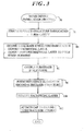
- FIG. 3 shows a flowchart of a fabrication process for producing either of the MEMS pressure sensor devices of FIGs. 1 and 2 in accordance with another embodiment
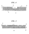
- FIG. 4 shows a side sectional view of a substrate structure fabricated in accordance with the process of FIG. 3 for incorporation in the MEMS pressure sensor device of FIG. 1 ;
- FIG. 5 shows a side sectional view of another substrate structure fabricated in accordance with the process of FIG. 3 for incorporation in the MEMS pressure sensor device of FIG. 1 ;
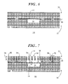
- FIG. 6 shows a side sectional view of the substrate structures of FIGs. 4 and 5 coupled together in a subsequent stage of processing
- FIG. 7 shows a side sectional view of the structure of FIG. 6 in a subsequent stage of processing
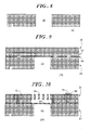
- FIG. 8 shows a side sectional view of a substrate structure fabricated in accordance with the process of FIG. 3 for incorporation in the MEMS pressure sensor device of FIG. 2 ;
- FIG. 9 shows a side sectional view of the substrate structures of FIGs. 5 and 8 coupled together in a subsequent stage of processing.
- FIG. 10 shows a side sectional view of the structure of FIG. 9 in a subsequent stage of processing.
- MEMS pressure sensor devices As the uses for MEMS pressure sensor devices continue to grow and diversify, increasing emphasis is being placed on the development of advanced silicon pressure sensors having enhanced sensitivity. In addition, increasing emphasis is being placed on fabrication methodology for MEMS pressure sensor devices that achieves this enhanced sensitivity without increasing manufacturing cost and complexity and without sacrificing part performance. These efforts are primarily driven by existing and potential high-volume applications in automotive, medical, commercial, and consumer products.
- An embodiment of the invention entails a microelectromechanical systems (MEMS) pressure sensor device that uses a diaphragm and a pressure cavity to create a variable capacitor to detect strain (or deflection) due to applied pressure over an area.
- Fabrication methodology for the MEMS pressure sensor device entails a stacked configuration of two substrate structures with the diaphragm formed as an intervening layer between the two substrate structures.
- the pressure sensor includes a buried pressure cavity, also referred to as a reference cavity, fabricated into one of the substrate structures.
- a sealed cavity is formed by coupling a cap wafer to one of the substrate structures to form the reference cavity.
- the fabrication methodology yields a MEMS pressure sensor device with enhanced sensitivity, that is durable, and that can be cost effectively fabricated utilizing existing manufacturing techniques.
- FIG. 1 shows a sectional side view of a microelectromechanical systems (MEMS) pressure sensor device 20 in accordance with an embodiment.
- MEMS microelectromechanical systems
- FIG. 1 and subsequent FIGs. 2 and 4-10 are illustrated using various shading and/or hatching to distinguish the different elements of MEMS pressure sensor device 20, as will be discussed below.
- These different elements within the structural layers may be produced utilizing current and upcoming micromachining techniques of depositing, patterning, etching, and so forth.
- Pressure sensor device 20 includes a first substrate structure 22, a second substrate structure 24 coupled to first substrate structure 22, and a cap 26 attached to second substrate structure 24.
- first and second used herein do not refer to an ordering or prioritization of elements within a countable series of elements. Rather, the terms “first” and “second” are used to distinguish the particular elements for clarity of discussion.
- First substrate structure 22 includes a first side 28 and a second side 30.
- a cavity 32 extends inwardly from second side 30 of first substrate structure 22.
- cavity 32 has a depth 34 that is less than a thickness 35 of first substrate structure 22. Accordingly, cavity 32 does not extend completely through first substrate structure 22.
- a reference element 36 is formed in second substrate structure 24 and is aligned with cavity 32.
- Reference element 36 includes a plurality of openings 38 extending through second substrate structure 24.
- Second substrate structure 24 further includes a first side 40 and a second side 42.
- a sense element 44 is disposed on first side 40 of second substrate structure 24, and is aligned with reference element 36. Thus, when first and second substrate structures 22 and 24, respectively, are coupled, sense element 44 is interposed between first and second substrate structures 22 and 24 and sense element 44 is also aligned with cavity 32.
- Cap 26 is attached to second side 42 of second substrate structure 24 to form a chamber 46 in which reference element 36 is located.
- Cap 26 includes a port 47 extending through cap 26 so that sense element 44 is exposed to an environment 48 external to MEMS pressure sensor device 20.
- MEMS sensor device 20 may additionally include one or more internal connection sites (not shown), conductive traces (not shown), conductive vias 50, and/or one or more external connection sites 52 (of which one is shown) that may be formed concurrently with other components of MEMS pressure sensor device 20 in accordance with design requirements for device 20.
- MEMS pressure sensor device 20 is configured to sense a pressure stimulus (P), represented by an arrow 54, from environment 48 external to MEMS pressure sensor device 20.
- Sense element 44 referred to hereinafter as a diaphragm 44, is exposed to external environment 48 via port 47 extending through cap 26 and subsequently via openings 38 in reference element 36.
- Diaphragm 44 is spaced apart from reference element 36 to form a gap 56 between sense element 44 and reference element 36.
- Diaphragm 44 is capable of movement in a direction 58 that is generally perpendicular to a plane of second substrate structure 24, e.g., first side 40 of second substrate structure 24, in response to pressure stimulus 54.
- Pressure sensor device 20 uses diaphragm 44 and the pressure within cavity 32 (typically less than atmospheric pressure) to create a variable capacitor to detect strain due to applied pressure, i.e., pressure stimulus 54.
- pressure sensor device 20 senses pressure stimulus 54 from environment 48 as movement of diaphragm 44 relative to reference element 36.
- a change in a capacitance 60 between reference element 36 and diaphragm 44 as a function of pressure stimulus 54 can be registered by sense circuitry (not shown) and converted to an output signal representative of pressure stimulus 54.
- Reference element 36 of pressure sensor 20 can serve an additional function.
- reference element 36 overlying diaphragm 44 may function as an over-travel stop that limits movement of diaphragm 44 in direction 58 when MEMS pressure sensor device 20 is subjected to harsh conditions so as to limit or prevent damage to diaphragm 44 and/or to prevent erroneous signals.
- FIG. 2 shows a sectional side view of a MEMS pressure sensor device 62 in accordance with another embodiment.
- Pressure sensor device 62 includes a first substrate structure 64, a second substrate structure (i.e., second substrate structure 24) coupled to first substrate structure 64, and a cap 66 attached to second substrate structure 24.
- First substrate structure 64 of device 62 differs from first substrate structure 22 of device 20 in that first substrate structure 64 has a cavity 68 that extends completely through thickness 35 of first substrate structure 64.
- the same second substrate structure 24 is implemented in each of MEMS sensor devices 20 and 62. Accordingly, a thorough description of second substrate structure 24 need not be repeated in connection with the description of pressure sensor device 62.
- reference element 36 of pressure sensor device 62 is aligned with cavity 68 of first substrate structure 64, and diaphragm 44 is aligned with reference element 36.
- Cap 66 is attached to second side 42 of second substrate structure 24 to form a chamber 70 in which reference element 36 is located.
- cap 66 does not include a port. Rather, diaphragm 44 is exposed to external environment 48 via cavity 68, and chamber 70 is a hermetically sealed cavity that serves as the reference pressure cavity at or near vacuum.
- diaphragm 44 and chamber 70 function cooperatively to create the variable capacitor for detecting strain due to applied pressure, i.e., pressure stimulus 54.
- diaphragm 44 having a thickness 72 that is significantly less than a thickness 74 of reference element 36.
- thickness 72 of diaphragm 44 may be less than fifteen percent of thickness 74 of reference element 36.
- thickness 72 of diaphragm 44 may be approximately two microns and thickness 74 of reference element 36 may be approximately twenty-five microns. This configuration enables the deflection of diaphragm 44 in response to pressure stimulus 54 relative to reference element 36.
- FIG. 3 shows a flowchart of a fabrication process 76 for producing either of the MEMS pressure sensor devices 20 and 62 ( FIGs. 1 and 2 ) in accordance with another embodiment.
- Fabrication process 76 implements known and developing MEMS micromachining technologies to cost effectively yield MEMS pressure sensor device 20 or 62 with enhanced pressure sensing sensitivity.
- Fabrication process 76 is described below in connection with the fabrication of a single MEMS pressure sensor device 20. However, it should be understood by those skilled in the art that the following process allows for concurrent wafer-level manufacturing of a plurality of MEMS pressure sensor devices 20, or alternatively, MEMS pressure sensor devices 62.
- the individual devices 20 can then be separated, cut, or diced in a conventional manner to provide individual MEMS pressure sensor devices 20 that can be packaged and integrated into an end application.
- MEMS sensor device fabrication process 76 begins with an activity 78. At activity 78, fabrication processes related to the formation of first substrate structure 22 are performed.
- FIG. 4 shows a side sectional view of first substrate structure 22 fabricated in accordance with process 76 for incorporation in MEMS pressure sensor device 20 ( FIG. 1 ).
- cavity 32 is formed in a silicon wafer 80, using for example a Deep Reactive Ion Etch (DRIE) technique, a Potassium Hydroxide (KOH) etch technique, or any suitable process, so that the depth of the cavity formed in wafer 80 is less than the thickness of wafer 80.
- DRIE Deep Reactive Ion Etch
- KOH Potassium Hydroxide
- a rightwardly and upwardly directed wide hatch pattern is utilized to represent wafer 80 in the various figures.
- Wafer 80 may subsequently be provided with one or more insulating or conductive layers.
- This layering is exemplified in FIG. 4 by the provision of a blanket insulating layer 82 of, for example, silicon oxide.
- Insulating layer 82 may be formed on each of first and second sides 28 and 30 and in cavity 32 by performing a local oxidation of silicon (LOCOS) microfabrication process or any other suitable process.
- LOC local oxidation of silicon
- a small stipple pattern is utilized to represent insulating layer 82 in the various figures. Other fabrication activities may be performed per convention that are not discussed or illustrated herein for clarity of description. Accordingly, at activity 78, first substrate structure 22 is produced with cavity 32 having depth 34 that is less than the final thickness 35 of first substrate structure 22.
- fabrication process 76 continues with an activity 84.
- fabrication processes related to the formation of second substrate structure 24 are performed.
- FIG. 5 shows a side sectional view of second substrate structure 24 fabricated in accordance with activity 84 of process 76 for incorporation in MEMS pressure sensor device 20 ( FIG. 1 ).
- MEMS pressure sensor device 62 FIG. 2
- second substrate structure 24, fabricated in accordance with process 76 may alternatively be incorporated in MEMS pressure sensor device 62 ( FIG. 2 ).
- fabrication of second substrate structure 24 entails the deposition of an insulating layer, referred to herein as a sacrificial layer 86, for example, silicon oxide, phosphosilicate glass (PSG), and the like on a wafer 88.
- a sacrificial layer 86 for example, silicon oxide, phosphosilicate glass (PSG), and the like
- a rightwardly and downwardly directed wide hatch pattern is utilized to represent wafer 88 in the various figures, and a small stipple pattern is again utilized to represent sacrificial layer 86 in the various figures.
- a material layer 90 is formed over sacrificial layer 86 by, for example, chemical vapor deposition, physical vapor deposition, or any other suitable process. Material layer 90 may then be selectively patterned and etched to form at least diaphragm 44 of MEMS pressure sensor device 20 ( FIG. 1 ). Material layer 90 may be, for example, polycrystalline silicon also referred to as polysilicon or simply poly, although other suitable materials may alternatively be utilized to form material layer 90. Material layer 90 may additionally be thinned and polished by performing, for example, Chemical-Mechanical Planarization (CMP) or another suitable process to yield diaphragm 44 having thickness 72 of, for example, two microns. A rightwardly and downwardly directed narrow hatch pattern is utilized to represent material layer 90 in the various figures.
- CMP Chemical-Mechanical Planarization
- MEMS device fabrication process 76 continues with an activity 92.
- activity 92 second substrate structure 24 ( FIG. 5 ) is coupled with first substrate structure 22 ( FIG. 4 ).
- FIG. 6 shows a side sectional view of first and second substrate structures 22 and 24 coupled in a subsequent stage 94 of processing.
- first and second substrate structures 22 and 24 are bonded together using, for example, a silicon direct bonding technique under vacuum.
- the pressure inside the wafer bonder when coupling first and second substrate structures 22 and 24 can be controlled by a mechanical pump so that a defined, i.e., predetermined, cavity pressure is produced inside of cavity 32.
- sense element 44 is interposed between first and second substrate structures 22 and 24, respectively, and cavity 32 is formed as a buried cavity with evacuated pressure. That is, a pressure within cavity 32 is significantly less than ambient or atmospheric pressure.
- MEMS device fabrication process 76 continues with an activity 96.
- reference element 36 ( FIG. 1 ) is formed in second substrate structure 24.
- FIG. 7 shows a side sectional view of the structure of FIG. 6 in a subsequent stage 98 of processing.
- activity 96 entails polishing or otherwise planarizing second side 42 of second substrate structure 24 to a final thickness 74 of, for example, approximately twenty-five microns.
- Wafer 88 of second substrate structure 24 is patterned by, for example, DRIE or KOH etching, so that openings 38 are created in reference element 36 overlying diaphragm 44 and cavity 32.
- openings 38 in reference element 36 serve as pressure vent holes so that diaphragm 44 is exposed to environment 48 ( FIG. 1 ), with or without cap 26 ( FIG. 1 ), for detection of pressure stimulus 54 ( FIG.
- Other processes that may be associated with activity 96 can include patterning, etching, and deposition of the appropriate materials to form conductive vias 50, external connection sites 52, internal connection sites (not shown), conductive traces (not shown) in accordance with design requirements for device 20.
- MEMS sensor device fabrication process 76 continues with an activity 100.
- activity 100 sacrificial layer 86 underlying reference element 36 is removed.
- sacrificial layer 86 has been removed between reference element 36 and diaphragm 44 so that gap 56 is formed between reference element 36 and diaphragm 44. Openings 38 in reference element 36 enable passage of an etch material, or etchant, in order to remove the underlying sacrificial layer 86 at activity 100.
- the etching of sacrificial layer 86 at activity 100 removes substantially an entirety of sacrificial layer 86 between reference element 36 and diaphragm 44 so that reference element 36 and diaphragm 44 are spaced apart from one another by gap 56.
- diaphragm 44 is free to move in response to external pressure stimulus 54 ( FIG. 1 ) in direction 58.
- cap 26 ( FIG. 1 ) having port 47 ( FIG. 1 ) may be attached to second side 42 of second substrate structure 24. Attachment of cap 26 to second substrate structure 24 may be accomplished using, for example, glass frit bonding, metal eutectic bonding, and the like.
- Process 76 may continue with other conventional fabrication activities (not shown). These additional fabrication activities may include packaging, forming electrical interconnects, testing, separation, and so forth. Following fabrication of MEMS pressure sensor device 20 ( FIG. 1 ), fabrication process 76 ends with a buried cavity 32 and a thin, highly sensitive diaphragm 44 having been formed using existing, cost effective, MEMS fabrication operations and using a wafer bonding technique.
- FIG. 8 shows a side sectional view of first substrate structure 64 fabricated in accordance with MEMS device fabrication process 76 ( FIG. 3 ) for incorporation in MEMS pressure sensor device 62 ( FIG. 2 ).
- FIG. 9 shows a side sectional view of first substrate structure 64 and second substrate structure 24 coupled in a subsequent stage 104 of processing.
- FIG. 10 shows a side sectional view of the structure of FIG. 9 in a subsequent stage 106 of processing.
- FIGs. 8-10 are presented herein to demonstrate the implementation of MEMS device fabrication process 76 ( FIG. 3 ) to fabricate MEMS pressure sensor device 62.
- cavity 68 is fabricated to extend through an entirety of first substrate structure 64.
- the remaining operations of fabricating second substrate structure 24 at activity 84 ( FIG. 3 ), coupling first and second substrate structures 64 and 24 at activity 92 ( FIG. 3 ), forming reference element 36 in second substrate structure 24 at activity 96 ( FIG. 3 ), removing sacrificial layer 86 at activity 100 ( FIG. 3 ), and attaching cap 66 ( FIG. 2 ) to second substrate structure 24 at activity 102 ( FIG. 3 ) remain largely unchanged.
- fabrication process 76 ends having cost effectively produced device 62 having a thin, highly sensitive diaphragm 44, cavity 68 functioning as a pressure port, and cap 66 being used to form a sealed cavity 70 ( FIG. 2 ).
- MEMS pressure sensor device 62 has also been formed using existing, cost effective MEMS fabrication operations and using a wafer bonding technique.
- Embodiments described herein comprise compact MEMS pressure sensor devices that use a diaphragm and a pressure cavity to create a variable capacitor to detect strain (or deflection) due to applied pressure over an area.
- Fabrication methodology for the MEMS pressure sensor devices entails a stacked configuration of two substrate structures with the diaphragm formed as an intervening layer between the two substrate structures.
- the MEMS pressure sensor device includes a buried reference cavity fabricated into one of the substrate structures.
- a sealed cavity is formed by coupling a cap wafer to one of the substrate structures to form the reference cavity.
- the fabrication methodology results in a thin diaphragm for enhanced sensitivity to a pressure stimulus, the efficient production of a hermetically sealed reference pressure chamber, and implementation of low cost existing MEMS batch processing techniques.
- the MEMS pressure sensor device and fabrication methodology achieves the additional advantages of good performance, small size, and low power consumption.
Landscapes
- Engineering & Computer Science (AREA)
- Microelectronics & Electronic Packaging (AREA)
- Manufacturing & Machinery (AREA)
- Physics & Mathematics (AREA)
- General Physics & Mathematics (AREA)
- Measuring Fluid Pressure (AREA)
- Micromachines (AREA)
- Pressure Sensors (AREA)
Abstract

Description
- The present invention is related to "MEMS Sensor Device With Multi-stimulus Sensing and Method of Fabricating Same," by Yizhen Lin, Woo Tae Park, Mark E. Schlarmann, and Hemant D. Desai filed on the same date as the present application, which is incorporated by reference herein.
- The present invention relates generally to microelectromechanical (MEMS) sensor devices. More specifically, the present invention relates to a method of fabricating a MEMS pressure sensor device.
- Microelectromechanical systems (MEMS) devices are semiconductor devices with embedded mechanical components. MEMS devices are used in products such as automobile airbag systems, control applications in automobiles, navigation, display systems, inkjet cartridges, and so forth. Capacitive-sensing MEMS device designs are highly desirable for operation in miniaturized devices due to their low temperature sensitivity, small size, and suitability for low cost mass production. One such MEMS device is a pressure sensor that measures pressure, typically of gases or liquids, for control and monitoring in many applications. One pressure sensor configuration uses a diaphragm and a pressure cavity to create a variable capacitor to detect strain (or deflection) due to applied pressure over an area. Common manufacturing technologies use metal, ceramic, and/or silicon diaphragms. Some prior art fabrication techniques yield structures that are undesirably thick and may therefore not function adequately as a movable diaphragm capable of detecting strain due to applied pressure. As such, these structures may have undesirably low sensitivity.
- A more complete understanding of the present invention may be derived by referring to the detailed description and claims when considered in connection with the Figures, wherein like reference numbers refer to similar items throughout the Figures, and:
-
FIG. 1 shows a sectional side view of a microelectromechanical systems (MEMS) pressure sensor device in accordance with an embodiment; -
FIG. 2 shows a sectional side view of a MEMS pressure sensor device in accordance with another embodiment; -
FIG. 3 shows a flowchart of a fabrication process for producing either of the MEMS pressure sensor devices ofFIGs. 1 and 2 in accordance with another embodiment; -
FIG. 4 shows a side sectional view of a substrate structure fabricated in accordance with the process ofFIG. 3 for incorporation in the MEMS pressure sensor device ofFIG. 1 ; -
FIG. 5 shows a side sectional view of another substrate structure fabricated in accordance with the process ofFIG. 3 for incorporation in the MEMS pressure sensor device ofFIG. 1 ; -
FIG. 6 shows a side sectional view of the substrate structures ofFIGs. 4 and 5 coupled together in a subsequent stage of processing; -
FIG. 7 shows a side sectional view of the structure ofFIG. 6 in a subsequent stage of processing; -
FIG. 8 shows a side sectional view of a substrate structure fabricated in accordance with the process ofFIG. 3 for incorporation in the MEMS pressure sensor device ofFIG. 2 ; -
FIG. 9 shows a side sectional view of the substrate structures ofFIGs. 5 and8 coupled together in a subsequent stage of processing; and -
FIG. 10 shows a side sectional view of the structure ofFIG. 9 in a subsequent stage of processing. - As the uses for MEMS pressure sensor devices continue to grow and diversify, increasing emphasis is being placed on the development of advanced silicon pressure sensors having enhanced sensitivity. In addition, increasing emphasis is being placed on fabrication methodology for MEMS pressure sensor devices that achieves this enhanced sensitivity without increasing manufacturing cost and complexity and without sacrificing part performance. These efforts are primarily driven by existing and potential high-volume applications in automotive, medical, commercial, and consumer products.
- An embodiment of the invention entails a microelectromechanical systems (MEMS) pressure sensor device that uses a diaphragm and a pressure cavity to create a variable capacitor to detect strain (or deflection) due to applied pressure over an area. Fabrication methodology for the MEMS pressure sensor device entails a stacked configuration of two substrate structures with the diaphragm formed as an intervening layer between the two substrate structures. In an embodiment, the pressure sensor includes a buried pressure cavity, also referred to as a reference cavity, fabricated into one of the substrate structures. In another embodiment, a sealed cavity is formed by coupling a cap wafer to one of the substrate structures to form the reference cavity. The fabrication methodology yields a MEMS pressure sensor device with enhanced sensitivity, that is durable, and that can be cost effectively fabricated utilizing existing manufacturing techniques.
-
FIG. 1 shows a sectional side view of a microelectromechanical systems (MEMS)pressure sensor device 20 in accordance with an embodiment.FIG. 1 and subsequentFIGs. 2 and4-10 are illustrated using various shading and/or hatching to distinguish the different elements of MEMSpressure sensor device 20, as will be discussed below. These different elements within the structural layers may be produced utilizing current and upcoming micromachining techniques of depositing, patterning, etching, and so forth. -
Pressure sensor device 20 includes afirst substrate structure 22, asecond substrate structure 24 coupled tofirst substrate structure 22, and acap 26 attached tosecond substrate structure 24. The terms "first" and "second" used herein do not refer to an ordering or prioritization of elements within a countable series of elements. Rather, the terms "first" and "second" are used to distinguish the particular elements for clarity of discussion. -
First substrate structure 22 includes afirst side 28 and asecond side 30. Acavity 32 extends inwardly fromsecond side 30 offirst substrate structure 22. In the illustrated embodiment,cavity 32 has adepth 34 that is less than athickness 35 offirst substrate structure 22. Accordingly,cavity 32 does not extend completely throughfirst substrate structure 22. - A
reference element 36 is formed insecond substrate structure 24 and is aligned withcavity 32.Reference element 36 includes a plurality ofopenings 38 extending throughsecond substrate structure 24.Second substrate structure 24 further includes afirst side 40 and asecond side 42. Asense element 44 is disposed onfirst side 40 ofsecond substrate structure 24, and is aligned withreference element 36. Thus, when first andsecond substrate structures sense element 44 is interposed between first andsecond substrate structures sense element 44 is also aligned withcavity 32. -
Cap 26 is attached tosecond side 42 ofsecond substrate structure 24 to form achamber 46 in whichreference element 36 is located.Cap 26 includes aport 47 extending throughcap 26 so thatsense element 44 is exposed to anenvironment 48 external to MEMSpressure sensor device 20. -
MEMS sensor device 20 may additionally include one or more internal connection sites (not shown), conductive traces (not shown),conductive vias 50, and/or one or more external connection sites 52 (of which one is shown) that may be formed concurrently with other components of MEMSpressure sensor device 20 in accordance with design requirements fordevice 20. - MEMS
pressure sensor device 20 is configured to sense a pressure stimulus (P), represented by anarrow 54, fromenvironment 48 external to MEMSpressure sensor device 20.Sense element 44, referred to hereinafter as adiaphragm 44, is exposed toexternal environment 48 viaport 47 extending throughcap 26 and subsequently viaopenings 38 inreference element 36.Diaphragm 44 is spaced apart fromreference element 36 to form agap 56 betweensense element 44 andreference element 36.Diaphragm 44 is capable of movement in adirection 58 that is generally perpendicular to a plane ofsecond substrate structure 24, e.g.,first side 40 ofsecond substrate structure 24, in response topressure stimulus 54. -
Pressure sensor device 20 usesdiaphragm 44 and the pressure within cavity 32 (typically less than atmospheric pressure) to create a variable capacitor to detect strain due to applied pressure, i.e.,pressure stimulus 54. As such,pressure sensor device 20senses pressure stimulus 54 fromenvironment 48 as movement ofdiaphragm 44 relative toreference element 36. A change in acapacitance 60 betweenreference element 36 anddiaphragm 44 as a function ofpressure stimulus 54 can be registered by sense circuitry (not shown) and converted to an output signal representative ofpressure stimulus 54.Reference element 36 ofpressure sensor 20 can serve an additional function. That is,reference element 36overlying diaphragm 44 may function as an over-travel stop that limits movement ofdiaphragm 44 indirection 58 when MEMSpressure sensor device 20 is subjected to harsh conditions so as to limit or prevent damage todiaphragm 44 and/or to prevent erroneous signals. -
FIG. 2 shows a sectional side view of a MEMSpressure sensor device 62 in accordance with another embodiment.Pressure sensor device 62 includes afirst substrate structure 64, a second substrate structure (i.e., second substrate structure 24) coupled tofirst substrate structure 64, and a cap 66 attached tosecond substrate structure 24.First substrate structure 64 ofdevice 62 differs fromfirst substrate structure 22 ofdevice 20 in thatfirst substrate structure 64 has acavity 68 that extends completely throughthickness 35 offirst substrate structure 64. However, the samesecond substrate structure 24 is implemented in each ofMEMS sensor devices second substrate structure 24 need not be repeated in connection with the description ofpressure sensor device 62. - Like pressure sensor device 20 (
FIG. 1 ),reference element 36 ofpressure sensor device 62 is aligned withcavity 68 offirst substrate structure 64, anddiaphragm 44 is aligned withreference element 36. Cap 66 is attached tosecond side 42 ofsecond substrate structure 24 to form achamber 70 in whichreference element 36 is located. In the illustrated embodiment, cap 66 does not include a port. Rather,diaphragm 44 is exposed toexternal environment 48 viacavity 68, andchamber 70 is a hermetically sealed cavity that serves as the reference pressure cavity at or near vacuum. Thus,diaphragm 44 andchamber 70 function cooperatively to create the variable capacitor for detecting strain due to applied pressure, i.e.,pressure stimulus 54. - Referring to
FIGs. 1 and 2 , fabrication methodology (discussed below) for MEMSpressure sensor devices thickness 72 that is significantly less than athickness 74 ofreference element 36. In some embodiments,thickness 72 ofdiaphragm 44 may be less than fifteen percent ofthickness 74 ofreference element 36. In a more particular embodiment,thickness 72 ofdiaphragm 44 may be approximately two microns andthickness 74 ofreference element 36 may be approximately twenty-five microns. This configuration enables the deflection ofdiaphragm 44 in response topressure stimulus 54 relative to referenceelement 36. -
FIG. 3 shows a flowchart of afabrication process 76 for producing either of the MEMSpressure sensor devices 20 and 62 (FIGs. 1 and 2 ) in accordance with another embodiment.Fabrication process 76 implements known and developing MEMS micromachining technologies to cost effectively yield MEMSpressure sensor device Fabrication process 76 is described below in connection with the fabrication of a single MEMSpressure sensor device 20. However, it should be understood by those skilled in the art that the following process allows for concurrent wafer-level manufacturing of a plurality of MEMSpressure sensor devices 20, or alternatively, MEMSpressure sensor devices 62. Theindividual devices 20 can then be separated, cut, or diced in a conventional manner to provide individual MEMSpressure sensor devices 20 that can be packaged and integrated into an end application. - MEMS sensor
device fabrication process 76 begins with anactivity 78. Atactivity 78, fabrication processes related to the formation offirst substrate structure 22 are performed. - Referring to
FIG. 4 in connection withactivity 78,FIG. 4 shows a side sectional view offirst substrate structure 22 fabricated in accordance withprocess 76 for incorporation in MEMS pressure sensor device 20 (FIG. 1 ). Atactivity 78,cavity 32 is formed in asilicon wafer 80, using for example a Deep Reactive Ion Etch (DRIE) technique, a Potassium Hydroxide (KOH) etch technique, or any suitable process, so that the depth of the cavity formed inwafer 80 is less than the thickness ofwafer 80. A rightwardly and upwardly directed wide hatch pattern is utilized to representwafer 80 in the various figures. -
Wafer 80 may subsequently be provided with one or more insulating or conductive layers. This layering is exemplified inFIG. 4 by the provision of ablanket insulating layer 82 of, for example, silicon oxide. Insulatinglayer 82 may be formed on each of first andsecond sides cavity 32 by performing a local oxidation of silicon (LOCOS) microfabrication process or any other suitable process. A small stipple pattern is utilized to represent insulatinglayer 82 in the various figures. Other fabrication activities may be performed per convention that are not discussed or illustrated herein for clarity of description. Accordingly, atactivity 78,first substrate structure 22 is produced withcavity 32 havingdepth 34 that is less than thefinal thickness 35 offirst substrate structure 22. - With reference back to
FIG. 3 ,fabrication process 76 continues with anactivity 84. Atactivity 84, fabrication processes related to the formation ofsecond substrate structure 24 are performed. - Referring now to
FIG. 5 in connection withactivity 84,FIG. 5 shows a side sectional view ofsecond substrate structure 24 fabricated in accordance withactivity 84 ofprocess 76 for incorporation in MEMS pressure sensor device 20 (FIG. 1 ). Of course, MEMS pressure sensor device 62 (FIG. 2 ) utilizes the same structure ofsecond substrate structure 24. Thus,second substrate structure 24, fabricated in accordance withprocess 76, may alternatively be incorporated in MEMS pressure sensor device 62 (FIG. 2 ). - In accordance with
activity 84, fabrication ofsecond substrate structure 24 entails the deposition of an insulating layer, referred to herein as asacrificial layer 86, for example, silicon oxide, phosphosilicate glass (PSG), and the like on awafer 88. A rightwardly and downwardly directed wide hatch pattern is utilized to representwafer 88 in the various figures, and a small stipple pattern is again utilized to representsacrificial layer 86 in the various figures. - Next, a
material layer 90 is formed oversacrificial layer 86 by, for example, chemical vapor deposition, physical vapor deposition, or any other suitable process.Material layer 90 may then be selectively patterned and etched to form atleast diaphragm 44 of MEMS pressure sensor device 20 (FIG. 1 ).Material layer 90 may be, for example, polycrystalline silicon also referred to as polysilicon or simply poly, although other suitable materials may alternatively be utilized to formmaterial layer 90.Material layer 90 may additionally be thinned and polished by performing, for example, Chemical-Mechanical Planarization (CMP) or another suitable process to yielddiaphragm 44 havingthickness 72 of, for example, two microns. A rightwardly and downwardly directed narrow hatch pattern is utilized to representmaterial layer 90 in the various figures. - With reference back to
FIG. 3 , followingfabrication activities device fabrication process 76 continues with anactivity 92. Atactivity 92, second substrate structure 24 (FIG. 5 ) is coupled with first substrate structure 22 (FIG. 4 ). - Referring now to
FIG. 6 in connection withactivity 92,FIG. 6 shows a side sectional view of first andsecond substrate structures subsequent stage 94 of processing. In an embodiment, first andsecond substrate structures second substrate structures cavity 32. Thus, once bonded,sense element 44 is interposed between first andsecond substrate structures cavity 32 is formed as a buried cavity with evacuated pressure. That is, a pressure withincavity 32 is significantly less than ambient or atmospheric pressure. - With reference back to
FIG. 3 , followingcoupling activity 92, MEMSdevice fabrication process 76 continues with anactivity 96. Atactivity 96, reference element 36 (FIG. 1 ) is formed insecond substrate structure 24. - Referring to
FIG. 7 in connection withactivity 96,FIG. 7 shows a side sectional view of the structure ofFIG. 6 in asubsequent stage 98 of processing. In an embodiment,activity 96 entails polishing or otherwise planarizingsecond side 42 ofsecond substrate structure 24 to afinal thickness 74 of, for example, approximately twenty-five microns.Wafer 88 ofsecond substrate structure 24 is patterned by, for example, DRIE or KOH etching, so thatopenings 38 are created inreference element 36 overlyingdiaphragm 44 andcavity 32. In the illustrated embodiment,openings 38 inreference element 36 serve as pressure vent holes so thatdiaphragm 44 is exposed to environment 48 (FIG. 1 ), with or without cap 26 (FIG. 1 ), for detection of pressure stimulus 54 (FIG. 1 ). Other processes that may be associated withactivity 96 can include patterning, etching, and deposition of the appropriate materials to formconductive vias 50,external connection sites 52, internal connection sites (not shown), conductive traces (not shown) in accordance with design requirements fordevice 20. - With reference back to
FIG. 3 , followingactivity 96, MEMS sensordevice fabrication process 76 continues with an activity 100. At activity 100,sacrificial layer 86underlying reference element 36 is removed. - Again referring to
FIG. 7 , atstage 98 of processing,sacrificial layer 86 has been removed betweenreference element 36 anddiaphragm 44 so thatgap 56 is formed betweenreference element 36 anddiaphragm 44.Openings 38 inreference element 36 enable passage of an etch material, or etchant, in order to remove the underlyingsacrificial layer 86 at activity 100. In an embodiment, the etching ofsacrificial layer 86 at activity 100 removes substantially an entirety ofsacrificial layer 86 betweenreference element 36 anddiaphragm 44 so thatreference element 36 anddiaphragm 44 are spaced apart from one another bygap 56. With the removal ofsacrificial layer 86 at activity 100,diaphragm 44 is free to move in response to external pressure stimulus 54 (FIG. 1 ) indirection 58. - With reference back to
FIG. 3 , following activity 100, MEMSdevice fabrication process 76 continues with anactivity 102. Atactivity 102, cap 26 (FIG. 1 ) having port 47 (FIG. 1 ) may be attached tosecond side 42 ofsecond substrate structure 24. Attachment ofcap 26 tosecond substrate structure 24 may be accomplished using, for example, glass frit bonding, metal eutectic bonding, and the like. -
Process 76 may continue with other conventional fabrication activities (not shown). These additional fabrication activities may include packaging, forming electrical interconnects, testing, separation, and so forth. Following fabrication of MEMS pressure sensor device 20 (FIG. 1 ),fabrication process 76 ends with a buriedcavity 32 and a thin, highlysensitive diaphragm 44 having been formed using existing, cost effective, MEMS fabrication operations and using a wafer bonding technique. - Referring to
FIGs. 8-10, FIG. 8 shows a side sectional view offirst substrate structure 64 fabricated in accordance with MEMS device fabrication process 76 (FIG. 3 ) for incorporation in MEMS pressure sensor device 62 (FIG. 2 ).FIG. 9 shows a side sectional view offirst substrate structure 64 andsecond substrate structure 24 coupled in asubsequent stage 104 of processing.FIG. 10 shows a side sectional view of the structure ofFIG. 9 in asubsequent stage 106 of processing. -
FIGs. 8-10 are presented herein to demonstrate the implementation of MEMS device fabrication process 76 (FIG. 3 ) to fabricate MEMSpressure sensor device 62. In particular, in this embodiment,cavity 68 is fabricated to extend through an entirety offirst substrate structure 64. However, the remaining operations of fabricatingsecond substrate structure 24 at activity 84 (FIG. 3 ), coupling first andsecond substrate structures FIG. 3 ), formingreference element 36 insecond substrate structure 24 at activity 96 (FIG. 3 ), removingsacrificial layer 86 at activity 100 (FIG. 3 ), and attaching cap 66 (FIG. 2 ) tosecond substrate structure 24 at activity 102 (FIG. 3 ) remain largely unchanged. - Again, following fabrication of MEMS pressure sensor device 62 (
FIG. 2 ),fabrication process 76 ends having cost effectively produceddevice 62 having a thin, highlysensitive diaphragm 44,cavity 68 functioning as a pressure port, and cap 66 being used to form a sealed cavity 70 (FIG. 2 ). Moreover, MEMSpressure sensor device 62 has also been formed using existing, cost effective MEMS fabrication operations and using a wafer bonding technique. - Embodiments described herein comprise compact MEMS pressure sensor devices that use a diaphragm and a pressure cavity to create a variable capacitor to detect strain (or deflection) due to applied pressure over an area. Fabrication methodology for the MEMS pressure sensor devices entails a stacked configuration of two substrate structures with the diaphragm formed as an intervening layer between the two substrate structures. In an embodiment, the MEMS pressure sensor device includes a buried reference cavity fabricated into one of the substrate structures. In another embodiment, a sealed cavity is formed by coupling a cap wafer to one of the substrate structures to form the reference cavity. The fabrication methodology results in a thin diaphragm for enhanced sensitivity to a pressure stimulus, the efficient production of a hermetically sealed reference pressure chamber, and implementation of low cost existing MEMS batch processing techniques. In addition, the MEMS pressure sensor device and fabrication methodology achieves the additional advantages of good performance, small size, and low power consumption.
- Although the preferred embodiments of the invention have been illustrated and described in detail, it will be readily apparent to those skilled in the art that various modifications may be made therein without departing from the spirit of the invention or from the scope of the appended claims.
Claims (15)
- A method (76) of producing a microelectromechanical systems (MEMS) sensor device (20, 62) comprising:forming (78) a first substrate structure (22) having a cavity (32);forming (84) a sense element (44) from a material layer (90) of a second substrate structure (24);coupling (92) said second substrate structure (24) with said first substrate structure (22) such that said sense element (44) is interposed between said first (22) and second (24) substrate structures and is aligned with said cavity (32); andforming (96) a reference element (36) in said second substrate structure (24) aligned with said sense element (44), said reference element (36) including a plurality of openings (38) extending through said second substrate structure (24), wherein said sense element (44) is exposed to an environment (48) external to said MEMS sensor device (20) via one of a group consisting of said cavity (32) and said plurality of openings (38).
- A method (76) as claimed in claim 1 wherein:said forming (84) said sense element (44) comprises depositing a sacrificial layer (86) on a surface of a wafer substrate (88) and depositing said material layer (90) on said sacrificial layer (86); andsaid method (76) further comprises removing (102) said sacrificial layer (86) between said reference element (36) and said sense element (44) via said plurality of openings (38) in said reference element (36) following said coupling operation (92), said removing operation (100) producing a gap (56) between said reference element (36) and said sense element (44).
- A method (76) as claimed in claims 1 or 2 wherein said forming (84) said sense element (44) includes producing said sense element having a first thickness (72) that is less than a second thickness (74) of said reference element (36).
- A method (76) as claimed in claims 1, 2, or 3 wherein said forming (78) said first substrate structure (22) produces said cavity (32) having a depth (34) that is less than a thickness (35) of said first substrate structure (22), and said sense element (44) is exposed to said environment (48) via said plurality of openings (38).
- A method (76) as claimed in claim 4 wherein said coupling operation (92) comprises controlling a cavity pressure of said cavity (32) such that said cavity pressure is less than atmospheric pressure.
- A method (76) as claimed in claim 5 wherein said material layer (90) is deposited on a first side (40) of said second substrate structure (24), and said method (76) further comprises attaching (102) a cap (26) to a second side (42) of said second substrate structure (24) to form a chamber (46) in which said reference element (36) is located; and
providing a port 47) extending through said cap (26) so that said sense element (44) is exposed to said environment (48) via said port (47). - A method (76) as claimed in claims 1, 2, 3, 4, 5, or 6 wherein said forming (78) said first substrate structure (64) produces said cavity (68) through a thickness of said first substrate structure (64), and said sense element (44) is exposed to said environment (48) via said cavity (68).
- A method (76) as claimed in claim 7 wherein said material layer (90) is deposited on a first side (40) of said second substrate structure (24), and said method (76) further comprises attaching (102) a cap (66) to a second side (42) of said second substrate structure (24) to form a hermetically sealed chamber (70) in which said reference element (36) is located.
- A microelectromechanical systems (MEMS) sensor device (20, 62) comprising;
a first substrate structure (22) having a cavity (32, 68) formed therein; and
a second substrate structure (24) having a reference element (36) formed in said second substrate structure (24) and aligned with said cavity (32), said reference element (36) including a plurality of openings (38) extending through said second substrate structure (24);
a sense element (44) disposed on a first side (40) of said second substrate structure (24) and aligned with said reference element (36), said sense element (44) being spaced apart from said reference element (36) to form a gap (56) between said sense element (44) and said reference element (36), said sense element (44) being exposed to an environment (48) external to said MEMS sensor device (20, 62) via one of a group consisting of said cavity (68) and said plurality of openings (38), and said sense element (44) being movable relative to said reference element (36) in response to a pressure stimulus (54) from said environment (48). - A MEMS sensor device (20, 62) as claimed in claim 9 wherein said sense element (44) exhibits a first thickness (72) that is less than a second thickness (74) of said reference element (36).
- A MEMS sensor device (20, 62) as claimed in claim 10 wherein said first thickness (72) is less than fifteen percent of said second thickness (74) of said reference element (36).
- A MEMS sensor device (20, 62) as claimed in claims 9, 10, or 11 wherein said cavity (32) has a depth (34) that is less than a thickness (35) of said first substrate structure (22), and said sense element (44) is exposed to said environment (48) via said plurality of openings (38).
- A MEMS sensor device (20, 62) as claimed in claim 12 further comprising a cap (26) attached to a second side (42) of said second substrate structure (24) to form a chamber (46) in which said reference element (36) is located, said cap (26) including a port (47) extending through said cap (26) so that said sense element (44) is exposed to said environment (48) via said port (47).
- A MEMS sensor device (20, 62) as claimed in claims 9, 10, 11, 12, or 13 wherein said cavity (68) extends through a thickness (35) of said first substrate structure (64), said sense element (44) being exposed to said environment (48) via said cavity (68), and said MEMS sensor device (20, 62) further comprises a cap (66) attached to a second side (42) of said second substrate structure (24) to form a hermetically sealed chamber (70) in which said reference element (36) is located.
- A MEMS sensor device (20, 62) as claimed in claims 9, 10, 11, 12, 13, and 14 wherein said sense element (44) and said reference element (36) form a capacitive pressure sensor.
Applications Claiming Priority (1)
| Application Number | Priority Date | Filing Date | Title |
|---|---|---|---|
| US12/861,435 US8316718B2 (en) | 2010-08-23 | 2010-08-23 | MEMS pressure sensor device and method of fabricating same |
Publications (2)
| Publication Number | Publication Date |
|---|---|
| EP2423157A2 true EP2423157A2 (en) | 2012-02-29 |
| EP2423157A3 EP2423157A3 (en) | 2012-03-07 |
Family
ID=44545541
Family Applications (1)
| Application Number | Title | Priority Date | Filing Date |
|---|---|---|---|
| EP11176316A Withdrawn EP2423157A3 (en) | 2010-08-23 | 2011-08-02 | MEMS pressure sensor device and method of fabricating same |
Country Status (4)
| Country | Link |
|---|---|
| US (1) | US8316718B2 (en) |
| EP (1) | EP2423157A3 (en) |
| JP (1) | JP5891571B2 (en) |
| CN (1) | CN102401706B (en) |
Cited By (3)
| Publication number | Priority date | Publication date | Assignee | Title |
|---|---|---|---|---|
| ITUA20162174A1 (en) * | 2016-03-31 | 2017-10-01 | St Microelectronics Srl | PROCESS OF MANUFACTURE OF A MEMS PRESSURE SENSOR AND RELATIVE MEMS PRESSURE SENSOR |
| IT201700045285A1 (en) * | 2017-04-26 | 2018-10-26 | St Microelectronics Srl | TRINCE-BASED MICROELETTROMECHANICAL TRANSDUCER AND METHOD OF MANUFACTURE OF THE MICROELECTRANCANICAL TRANSDUCER |
| US10935444B2 (en) | 2017-04-21 | 2021-03-02 | Stmicroelectronics S.R.L. | Stress sensor for monitoring the health state of fabricated structures such as constructions, buildings, infrastructures and the like |
Families Citing this family (46)
| Publication number | Priority date | Publication date | Assignee | Title |
|---|---|---|---|---|
| EP2523896B1 (en) * | 2010-01-11 | 2014-06-11 | ELMOS Semiconductor AG | Micro-electromechanical semiconductor component and method for the production thereof |
| US8461656B2 (en) | 2010-06-30 | 2013-06-11 | Freescale Semiconductor, Inc. | Device structures for in-plane and out-of-plane sensing micro-electro-mechanical systems (MEMS) |
| US8476087B2 (en) | 2011-04-21 | 2013-07-02 | Freescale Semiconductor, Inc. | Methods for fabricating sensor device package using a sealing structure |
| US8384168B2 (en) | 2011-04-21 | 2013-02-26 | Freescale Semiconductor, Inc. | Sensor device with sealing structure |
| FR2977319B1 (en) * | 2011-07-01 | 2014-03-14 | Commissariat Energie Atomique | OPTIMIZED SENSIBLITY PRESSURE MEASURING DEVICE |
| JP5708535B2 (en) * | 2012-03-13 | 2015-04-30 | 株式会社デンソー | Angular velocity sensor |
| US9046546B2 (en) | 2012-04-27 | 2015-06-02 | Freescale Semiconductor Inc. | Sensor device and related fabrication methods |
| US20130307147A1 (en) * | 2012-05-18 | 2013-11-21 | Xintec Inc. | Chip package and method for forming the same |
| DE102013020388A1 (en) * | 2012-12-13 | 2014-06-18 | Tesat-Spacecom Gmbh & Co. Kg | Method for checking the density of a housing |
| US9562820B2 (en) | 2013-02-28 | 2017-02-07 | Mks Instruments, Inc. | Pressure sensor with real time health monitoring and compensation |
| US8802473B1 (en) * | 2013-03-14 | 2014-08-12 | Taiwan Semiconductor Manufacturing Company, Ltd. | MEMS integrated pressure sensor devices having isotropic cavities and methods of forming same |
| JP6127625B2 (en) * | 2013-03-19 | 2017-05-17 | オムロン株式会社 | Capacitance type pressure sensor and input device |
| GB2513594B (en) * | 2013-04-30 | 2015-09-02 | Kidde Tech Inc | Method of manufacturing a pressure sensor |
| US9034679B2 (en) * | 2013-06-25 | 2015-05-19 | Freescale Semiconductor, Inc. | Method for fabricating multiple types of MEMS devices |
| DE102013213071B3 (en) * | 2013-07-04 | 2014-10-09 | Robert Bosch Gmbh | Manufacturing method for a micromechanical component |
| US10273147B2 (en) | 2013-07-08 | 2019-04-30 | Motion Engine Inc. | MEMS components and method of wafer-level manufacturing thereof |
| WO2015013827A1 (en) | 2013-08-02 | 2015-02-05 | Motion Engine Inc. | Mems motion sensor for sub-resonance angular rate sensing |
| US9617150B2 (en) * | 2013-10-09 | 2017-04-11 | Taiwan Semiconductor Manufacturing Co., Ltd. | Micro-electro mechanical system (MEMS) device having a blocking layer formed between closed chamber and a dielectric layer of a CMOS substrate |
| US20150102437A1 (en) * | 2013-10-14 | 2015-04-16 | Freescale Semiconductor, Inc. | Mems sensor device with multi-stimulus sensing and method of fabrication |
| US9285289B2 (en) * | 2013-12-06 | 2016-03-15 | Freescale Semiconductor, Inc. | Pressure sensor with built-in calibration capability |
| CN103616098B (en) * | 2013-12-06 | 2015-08-26 | 西安交通大学 | A kind of high precision is based on the flexure electric-type pressure transducer of metallic elastic component |
| DE102014200500A1 (en) * | 2014-01-14 | 2015-07-16 | Robert Bosch Gmbh | Micromechanical pressure sensor device and corresponding manufacturing method |
| US9438979B2 (en) * | 2014-03-06 | 2016-09-06 | Infineon Technologies Ag | MEMS sensor structure for sensing pressure waves and a change in ambient pressure |
| CN104981101B (en) * | 2014-04-03 | 2019-05-03 | 欣兴电子股份有限公司 | Embedded element structure and manufacturing method thereof |
| US20170030788A1 (en) * | 2014-04-10 | 2017-02-02 | Motion Engine Inc. | Mems pressure sensor |
| US11674803B2 (en) | 2014-06-02 | 2023-06-13 | Motion Engine, Inc. | Multi-mass MEMS motion sensor |
| US9369804B2 (en) * | 2014-07-28 | 2016-06-14 | Robert Bosch Gmbh | MEMS membrane overtravel stop |
| JP6799529B2 (en) * | 2014-08-28 | 2020-12-16 | マイクロドース セラピューテクス,インコーポレイテッド | Tidal dry powder inhaler with small pressure sensor activation |
| US10023461B2 (en) * | 2014-10-31 | 2018-07-17 | Stmicroelectronics S.R.L. | Microintegrated encapsulated MEMS sensor with mechanical decoupling and manufacturing process thereof |
| TWI513981B (en) | 2014-11-13 | 2015-12-21 | Ind Tech Res Inst | Mems apparatus with multiple chambers and method for manufacturing the same |
| KR101620352B1 (en) | 2014-12-05 | 2016-05-13 | 주식회사 현대케피코 | Fuel Supply System with Pressure Sensor |
| US11287486B2 (en) | 2014-12-09 | 2022-03-29 | Motion Engine, Inc. | 3D MEMS magnetometer and associated methods |
| US9663350B2 (en) * | 2014-12-12 | 2017-05-30 | Nxp Usa, Inc. | Stress isolated differential pressure sensor |
| US10407299B2 (en) | 2015-01-15 | 2019-09-10 | Motion Engine Inc. | 3D MEMS device with hermetic cavity |
| CN104634487B (en) * | 2015-02-16 | 2017-05-31 | 迈尔森电子(天津)有限公司 | Mems pressure sensor and forming method thereof |
| CN104655334B (en) * | 2015-02-16 | 2017-05-03 | 迈尔森电子(天津)有限公司 | MEMS (micro-electro mechanical system) pressure sensor and forming method thereof |
| DE102015211778A1 (en) * | 2015-06-25 | 2016-12-29 | Robert Bosch Gmbh | Method for producing a micromechanical structure and a component with this micromechanical structure |
| CN104897334B (en) * | 2015-06-29 | 2017-07-21 | 歌尔股份有限公司 | A kind of MEMS pressure sensors |
| CN104966689B (en) * | 2015-07-17 | 2017-07-07 | 安徽北方芯动联科微系统技术有限公司 | A kind of hood-opening device and ends-opening method of the MEMS chip of wafer level packaging |
| US10648879B2 (en) | 2016-02-22 | 2020-05-12 | Kathirgamasundaram Sooriakumar | Capacitive pressure sensor |
| IT201700035969A1 (en) | 2017-03-31 | 2018-10-01 | St Microelectronics Srl | MEMS DEVICE INCLUDING A CAPACITIVE TYPE PRESSURE SENSOR AND RELATIVE PROCESS OF PROCESSING |
| CN112512959A (en) * | 2018-08-09 | 2021-03-16 | Lpkf激光电子股份公司 | Method for producing a microstructure |
| DE102018222738A1 (en) * | 2018-12-21 | 2020-06-25 | Robert Bosch Gmbh | Micromechanical pressure sensor device and a corresponding manufacturing method |
| JP2024002882A (en) * | 2022-06-24 | 2024-01-11 | ローム株式会社 | Pressure sensor and pressure sensor manufacturing method |
| CN119178552A (en) * | 2024-08-09 | 2024-12-24 | 中北大学 | Capacitance film vacuum gauge and preparation method thereof |
| CN119430071B (en) * | 2024-11-20 | 2025-12-02 | 苏州园芯微电子技术有限公司 | An integrated MEMS chip and its manufacturing method |
Citations (2)
| Publication number | Priority date | Publication date | Assignee | Title |
|---|---|---|---|---|
| US20070065968A1 (en) * | 2003-05-26 | 2007-03-22 | Kit-Wai Kok | Fabrication of silicon microphone |
| DE102006011545A1 (en) * | 2006-03-14 | 2007-09-20 | Robert Bosch Gmbh | Micromechanical combination unit for use in mobile telephone position-dependent display control, has inertia type and diaphragm type sensor devices formed on front side of substrate, where diaphragm type sensor device has diaphragm |
Family Cites Families (12)
| Publication number | Priority date | Publication date | Assignee | Title |
|---|---|---|---|---|
| FR2715502B1 (en) | 1994-01-26 | 1996-04-05 | Commissariat Energie Atomique | Structure having cavities and method for producing such a structure. |
| FI115500B (en) | 2000-03-21 | 2005-05-13 | Nokia Oyj | Method of manufacturing a membrane detector |
| JP2004356707A (en) * | 2003-05-27 | 2004-12-16 | Hosiden Corp | Sound detection mechanism |
| US6939473B2 (en) | 2003-10-20 | 2005-09-06 | Invensense Inc. | Method of making an X-Y axis dual-mass tuning fork gyroscope with vertically integrated electronics and wafer-scale hermetic packaging |
| WO2005054804A1 (en) | 2003-12-04 | 2005-06-16 | National University Of Singapore | Capacitive pressure sensor with a cantilever member |
| US8569850B2 (en) * | 2006-10-11 | 2013-10-29 | Sensfab Pte Ltd | Ultra low pressure sensor |
| US20090154764A1 (en) | 2006-10-20 | 2009-06-18 | Forhealth Technologies, Inc. | Drug vial detection in an automated drug preparation system |
| KR101411416B1 (en) | 2007-12-14 | 2014-06-26 | 삼성전자주식회사 | Micro speaker manufacturing method and micro speaker |
| US8211751B2 (en) * | 2007-12-25 | 2012-07-03 | Fujikura Ltd. | Semiconductor device and method of manufacturing the same |
| US8193596B2 (en) * | 2008-09-03 | 2012-06-05 | Solid State System Co., Ltd. | Micro-electro-mechanical systems (MEMS) package |
| US8220330B2 (en) * | 2009-03-24 | 2012-07-17 | Freescale Semiconductor, Inc. | Vertically integrated MEMS sensor device with multi-stimulus sensing |
| US8387464B2 (en) * | 2009-11-30 | 2013-03-05 | Freescale Semiconductor, Inc. | Laterally integrated MEMS sensor device with multi-stimulus sensing |
-
2010
- 2010-08-23 US US12/861,435 patent/US8316718B2/en not_active Expired - Fee Related
-
2011
- 2011-07-29 JP JP2011167449A patent/JP5891571B2/en not_active Expired - Fee Related
- 2011-08-02 EP EP11176316A patent/EP2423157A3/en not_active Withdrawn
- 2011-08-22 CN CN201110240721.6A patent/CN102401706B/en not_active Expired - Fee Related
Patent Citations (2)
| Publication number | Priority date | Publication date | Assignee | Title |
|---|---|---|---|---|
| US20070065968A1 (en) * | 2003-05-26 | 2007-03-22 | Kit-Wai Kok | Fabrication of silicon microphone |
| DE102006011545A1 (en) * | 2006-03-14 | 2007-09-20 | Robert Bosch Gmbh | Micromechanical combination unit for use in mobile telephone position-dependent display control, has inertia type and diaphragm type sensor devices formed on front side of substrate, where diaphragm type sensor device has diaphragm |
Cited By (8)
| Publication number | Priority date | Publication date | Assignee | Title |
|---|---|---|---|---|
| ITUA20162174A1 (en) * | 2016-03-31 | 2017-10-01 | St Microelectronics Srl | PROCESS OF MANUFACTURE OF A MEMS PRESSURE SENSOR AND RELATIVE MEMS PRESSURE SENSOR |
| EP3225586A1 (en) * | 2016-03-31 | 2017-10-04 | STMicroelectronics Srl | Process for manufacturing a mems pressure sensor, and corresponding mems pressure sensor |
| US10048148B2 (en) | 2016-03-31 | 2018-08-14 | Stmicroelectronics S.R.L. | Process for manufacturing a MEMS pressure sensor, and corresponding MEMS pressure sensor |
| US10578505B2 (en) | 2016-03-31 | 2020-03-03 | Stmicroelectronics S.R.L. | Process for manufacturing a MEMS pressure sensor, and corresponding MEMS pressure sensor |
| US10935444B2 (en) | 2017-04-21 | 2021-03-02 | Stmicroelectronics S.R.L. | Stress sensor for monitoring the health state of fabricated structures such as constructions, buildings, infrastructures and the like |
| IT201700045285A1 (en) * | 2017-04-26 | 2018-10-26 | St Microelectronics Srl | TRINCE-BASED MICROELETTROMECHANICAL TRANSDUCER AND METHOD OF MANUFACTURE OF THE MICROELECTRANCANICAL TRANSDUCER |
| EP3396344A1 (en) * | 2017-04-26 | 2018-10-31 | STMicroelectronics S.r.l. | Trench-based microelectromechanical transducer and method for manufacturing thereof |
| US10737929B2 (en) * | 2017-04-26 | 2020-08-11 | Stmicroelectronics S.R.L. | Trench-based microelectromechanical transducer and method for manufacturing the microelectromechanical transducer |
Also Published As
| Publication number | Publication date |
|---|---|
| US8316718B2 (en) | 2012-11-27 |
| US20120042731A1 (en) | 2012-02-23 |
| EP2423157A3 (en) | 2012-03-07 |
| JP5891571B2 (en) | 2016-03-23 |
| CN102401706A (en) | 2012-04-04 |
| CN102401706B (en) | 2016-03-09 |
| JP2012042460A (en) | 2012-03-01 |
Similar Documents
| Publication | Publication Date | Title |
|---|---|---|
| US8316718B2 (en) | MEMS pressure sensor device and method of fabricating same | |
| US8216882B2 (en) | Method of producing a microelectromechanical (MEMS) sensor device | |
| EP2011132B1 (en) | Capacitive micro- electro- mechanical sensors with single crystal silicon electrodes | |
| US9550668B1 (en) | Integrated MEMS pressure sensor and MEMS inertial sensor | |
| US8387464B2 (en) | Laterally integrated MEMS sensor device with multi-stimulus sensing | |
| US7998777B1 (en) | Method for fabricating a sensor | |
| EP1594800B1 (en) | Method of manufacturing an electronic device and electronic device | |
| US20150102437A1 (en) | Mems sensor device with multi-stimulus sensing and method of fabrication | |
| US20070202628A1 (en) | Manufacturing process for integrated piezo elements | |
| EP3052901B1 (en) | Inertial and pressure sensors on single chip | |
| US20090325335A1 (en) | Heterogeneous substrate including a sacrificial layer, and a method of fabricating it | |
| US6768628B2 (en) | Method for fabricating an isolated microelectromechanical system (MEMS) device incorporating a wafer level cap | |
| CN103771333A (en) | A method for manufacturing a cap for a MEMS component, and hybrid integrated component having such a cap | |
| US8461656B2 (en) | Device structures for in-plane and out-of-plane sensing micro-electro-mechanical systems (MEMS) | |
| US7192819B1 (en) | Semiconductor sensor device using MEMS technology | |
| CN116750709B (en) | MEMS acceleration and pressure integrated sensor and preparation method thereof | |
| EP4144687B1 (en) | Method for manufacturing an integrated system including a capacitive pressure sensor and an inertial sensor, and integrated system | |
| US20150291414A1 (en) | Mems device having conductive microstructures laterally surrounded by oxide material | |
| US10775253B2 (en) | Method for producing a micromechanical component with an exposed pressure sensor device and micromechanical component | |
| CN100524614C (en) | Method of manufacturing an electronic device and electronic device | |
| EP4488224A1 (en) | Microelectromechanical sensor device with wafer-level integration of pressure and inertial detection structures and corresponding manufacturing process | |
| CN119218934A (en) | Micro-electromechanical sensor device with wafer-level integration and corresponding manufacturing method | |
| CN112504548A (en) | Composite sensor, processing method thereof and TPMS chip | |
| CN113776721A (en) | Sensor integrated chip and manufacturing method thereof |
Legal Events
| Date | Code | Title | Description |
|---|---|---|---|
| PUAL | Search report despatched |
Free format text: ORIGINAL CODE: 0009013 |
|
| AK | Designated contracting states |
Kind code of ref document: A2 Designated state(s): AL AT BE BG CH CY CZ DE DK EE ES FI FR GB GR HR HU IE IS IT LI LT LU LV MC MK MT NL NO PL PT RO RS SE SI SK SM TR |
|
| AX | Request for extension of the european patent |
Extension state: BA ME |
|
| PUAI | Public reference made under article 153(3) epc to a published international application that has entered the european phase |
Free format text: ORIGINAL CODE: 0009012 |
|
| AK | Designated contracting states |
Kind code of ref document: A3 Designated state(s): AL AT BE BG CH CY CZ DE DK EE ES FI FR GB GR HR HU IE IS IT LI LT LU LV MC MK MT NL NO PL PT RO RS SE SI SK SM TR |
|
| AX | Request for extension of the european patent |
Extension state: BA ME |
|
| RIC1 | Information provided on ipc code assigned before grant |
Ipc: G01L 9/00 20060101ALI20120131BHEP Ipc: H04R 19/00 20060101ALI20120131BHEP Ipc: G01L 19/06 20060101ALI20120131BHEP Ipc: B81C 1/00 20060101AFI20120131BHEP |
|
| 17P | Request for examination filed |
Effective date: 20120907 |
|
| RAP1 | Party data changed (applicant data changed or rights of an application transferred) |
Owner name: NORTH STAR INNOVATIONS INC. |
|
| 17Q | First examination report despatched |
Effective date: 20160923 |
|
| STAA | Information on the status of an ep patent application or granted ep patent |
Free format text: STATUS: THE APPLICATION IS DEEMED TO BE WITHDRAWN |
|
| 18D | Application deemed to be withdrawn |
Effective date: 20170204 |