EP2422585B1 - Optoelektronische folienanordnung - Google Patents
Optoelektronische folienanordnung Download PDFInfo
- Publication number
- EP2422585B1 EP2422585B1 EP10718869.0A EP10718869A EP2422585B1 EP 2422585 B1 EP2422585 B1 EP 2422585B1 EP 10718869 A EP10718869 A EP 10718869A EP 2422585 B1 EP2422585 B1 EP 2422585B1
- Authority
- EP
- European Patent Office
- Prior art keywords
- layer
- fabric
- electrode
- electrode layer
- fibres
- Prior art date
- Legal status (The legal status is an assumption and is not a legal conclusion. Google has not performed a legal analysis and makes no representation as to the accuracy of the status listed.)
- Not-in-force
Links
Images

Classifications
-
- H—ELECTRICITY
- H05—ELECTRIC TECHNIQUES NOT OTHERWISE PROVIDED FOR
- H05B—ELECTRIC HEATING; ELECTRIC LIGHT SOURCES NOT OTHERWISE PROVIDED FOR; CIRCUIT ARRANGEMENTS FOR ELECTRIC LIGHT SOURCES, IN GENERAL
- H05B33/00—Electroluminescent light sources
- H05B33/12—Light sources with substantially two-dimensional [2D] radiating surfaces
- H05B33/26—Light sources with substantially two-dimensional [2D] radiating surfaces characterised by the composition or arrangement of the conductive material used as an electrode
- H05B33/28—Light sources with substantially two-dimensional [2D] radiating surfaces characterised by the composition or arrangement of the conductive material used as an electrode of translucent electrodes
-
- H—ELECTRICITY
- H05—ELECTRIC TECHNIQUES NOT OTHERWISE PROVIDED FOR
- H05B—ELECTRIC HEATING; ELECTRIC LIGHT SOURCES NOT OTHERWISE PROVIDED FOR; CIRCUIT ARRANGEMENTS FOR ELECTRIC LIGHT SOURCES, IN GENERAL
- H05B33/00—Electroluminescent light sources
- H05B33/12—Light sources with substantially two-dimensional [2D] radiating surfaces
- H05B33/14—Light sources with substantially two-dimensional [2D] radiating surfaces characterised by the chemical or physical composition or the arrangement of the electroluminescent material, or by the simultaneous addition of the electroluminescent material in or onto the light source
-
- H—ELECTRICITY
- H10—SEMICONDUCTOR DEVICES; ELECTRIC SOLID-STATE DEVICES NOT OTHERWISE PROVIDED FOR
- H10K—ORGANIC ELECTRIC SOLID-STATE DEVICES
- H10K30/00—Organic devices sensitive to infrared radiation, light, electromagnetic radiation of shorter wavelength or corpuscular radiation
- H10K30/80—Constructional details
- H10K30/81—Electrodes
- H10K30/82—Transparent electrodes, e.g. indium tin oxide [ITO] electrodes
-
- H—ELECTRICITY
- H10—SEMICONDUCTOR DEVICES; ELECTRIC SOLID-STATE DEVICES NOT OTHERWISE PROVIDED FOR
- H10K—ORGANIC ELECTRIC SOLID-STATE DEVICES
- H10K77/00—Constructional details of devices covered by this subclass and not covered by groups H10K10/80, H10K30/80, H10K50/80 or H10K59/80
- H10K77/10—Substrates, e.g. flexible substrates
- H10K77/111—Flexible substrates
-
- Y—GENERAL TAGGING OF NEW TECHNOLOGICAL DEVELOPMENTS; GENERAL TAGGING OF CROSS-SECTIONAL TECHNOLOGIES SPANNING OVER SEVERAL SECTIONS OF THE IPC; TECHNICAL SUBJECTS COVERED BY FORMER USPC CROSS-REFERENCE ART COLLECTIONS [XRACs] AND DIGESTS
- Y02—TECHNOLOGIES OR APPLICATIONS FOR MITIGATION OR ADAPTATION AGAINST CLIMATE CHANGE
- Y02E—REDUCTION OF GREENHOUSE GAS [GHG] EMISSIONS, RELATED TO ENERGY GENERATION, TRANSMISSION OR DISTRIBUTION
- Y02E10/00—Energy generation through renewable energy sources
- Y02E10/50—Photovoltaic [PV] energy
- Y02E10/549—Organic PV cells
-
- Y—GENERAL TAGGING OF NEW TECHNOLOGICAL DEVELOPMENTS; GENERAL TAGGING OF CROSS-SECTIONAL TECHNOLOGIES SPANNING OVER SEVERAL SECTIONS OF THE IPC; TECHNICAL SUBJECTS COVERED BY FORMER USPC CROSS-REFERENCE ART COLLECTIONS [XRACs] AND DIGESTS
- Y02—TECHNOLOGIES OR APPLICATIONS FOR MITIGATION OR ADAPTATION AGAINST CLIMATE CHANGE
- Y02P—CLIMATE CHANGE MITIGATION TECHNOLOGIES IN THE PRODUCTION OR PROCESSING OF GOODS
- Y02P70/00—Climate change mitigation technologies in the production process for final industrial or consumer products
- Y02P70/50—Manufacturing or production processes characterised by the final manufactured product
Definitions
- the present invention relates to an optoelectronic film assembly, in particular electroluminescent (EL) film, according to the preamble of the main claim.
- EL electroluminescent
- Such devices are well known in the art and are used because of their favorable surface lighting properties in conjunction with low power consumption and long illumination in a variety of applications, especially for the realization of warning or signal surfaces in lighting, advertising, design and architecture.
- Sheet-like, sheet-like electroluminescent devices are based on the functional principle that a so-called active layer, typically made of doped zinc sulfide as electroluminescent material and a dielectric layer is provided in the manner of a plate capacitor between two planar electrodes and this arrangement when energized with an AC signal ( typical frequency between about 200 Hz and 4 kHz) performs a cold, areal and non-directional light emission.
- an AC signal typical frequency between about 200 Hz and 4 kHz
- the amplitude and frequency of the applied AC voltage can alter the brightness (and, in limits, the color) of the light emission.
- EL foil arrangements typically as a first electrode on a polymer substrate which with indium tin oxide (indium tin oxide ITO, as realization of a transparent, conductive oxide (TCO)), typically by vacuum sputtering, is coated so that a conductive, yet transparent electrode layer is formed.
- indium tin oxide indium tin oxide ITO, as realization of a transparent, conductive oxide (TCO)
- TCO transparent, conductive oxide
- an active layer of electroluminescent material is provided towards an equally planar and typically opaque counter electrode, such as a printed circuit board, typically by use of zinc sulfite doped with suitable metals such as gold, silver, copper, gallium or manganese ,
- a dielectric applied thereto Layer for example, barium titanate, prevents short-circuiting of the electrodes, when the (typically opaque) counter-electrode completes the generic known foil arrangement.
- WO 2005/062679 A1 has a foil assembly including two electrode layers, an intermediate dielectric layer and a dielectric layer adjacent active layer.
- both electrode layers which contain neither TCO nor ITO and consist of a fabric comprising electrically conductive fibers, can be translucent.
- the.transparente ITO PET front electrode proves to be cost-critical, moreover, it is brittle.
- ITO must be applied as a very thin layer in order to be sufficiently optically transparent, which in turn suffers from the electrical conductivity (and is thus typically higher than 50 ⁇ / sq, thus having not inconsiderable electrical resistance properties).
- a power or connection rail to ensure the electrical connection.
- one dimension of the product is fixed, so that a continuous, endless production process (with the corresponding cost and quantity advantages) is eliminated.
- the problem of limited dimensions with which uniform brightness is achieved, and by the structure described is a maximum cutoff frequency for driving is limited.
- the object of the present invention is therefore to provide an alternative film arrangement for realizing an electroluminescent film, which is optimized in particular with regard to the production outlay and the necessity of expensive materials for realizing a transparent electrode surface. Furthermore, a new or improved method for producing an EL foil arrangement is to be created.
- the object is achieved by the optoelectronic film arrangement having the features of the main claim, the method for producing an optoelectronic film arrangement having the features of independent patent claim 7 and a use of the optoelectronic film arrangement for producing lighting and / or signaling devices for entertainment and / or household electronics Having solved construction, trade fair, architecture, security and / or transportation, including aviation.
- Advantageous developments of the invention are described in the subclaims.
- At least one of the two electrode layers, or both has a fabric which has electrically conductive fibers.
- This tissue thus offers the possibility to realize the electrode functionality efficiently and inexpensively, whereby at the same time - by suitable design of the tissue in the choice of the respective fiber thickness, the design of the spaces between the fibers and the type of electrically conductive fibers (Fibern) - Possibilities for the design of the desired properties and for adaptation to a particular intended use of the optoelectronic film arrangement are made possible in a very flexible manner. In addition, this arrangement is flexible and almost arbitrarily malleable.
- the fabric against moisture or other environmental influences, to embed this (at least partially) in a transparent, electrically non-conductive polymer material.
- a transparent, electrically non-conductive polymer material not only (for example, by appropriate coloring This polymer material), the light color can be influenced, also, by suitable selection of the polymer material, the electrode (and thus the overall arrangement) weatherproof.
- thermosetting resin for practical implementation of the coating for the fibers, it is within the scope of preferred developments of the invention possible to design these in the form of a radiation-curing, supplementary or alternatively, thermosetting resin, wherein an acrylic resin, a silicone material, a fluoropolymer may be suitable, as well as a polymer selected from a group consisting of PU, PEN, PI, PET, PA, EVA or similar materials.
- fibers (fibers) With regard to the fibers (fibers) according to the invention, it is first encompassed by the invention to produce the fabric substantially from electrically non-conductive fibers, which are then provided with an electrical conductivity for realizing the electrode effect.
- Suitable fibers (fibers) are in particular transparent or semitransparent monofilaments of PA, PP, PET, PEEK, PI, PPS or similar chemical fibers. This allows significant cost advantages compared to pure metal fibers (with comparable electrical conduction properties); In addition, these cost advantages are realized particularly drastically in comparison to the generic ITO coating.
- the fabric used has a sheet resistance ⁇ 50 ⁇ / sq, preferably ⁇ 20 ⁇ / sq, more preferably less than 10 ⁇ / sq
- it is on the one hand of the invention comprises, further training to provide fibers in the fabric, which are made of metal consist of (metal fibers), or as fibers that carry a metallization.
- the metallization advantageously has a layer thickness in the range between 100 nm and 10 ⁇ m, in particular between 200 nm and 3 ⁇ m.
- Suitable metals for the realization of the metallized or metal fibers are, for example, Ti, Ag, Al, Cu, Au, Pa, Pt, Ni, W, Mo, Nb, Ba, Sn, Zr or the like, wherein the conductivity of the fabric (resp The surface resistance) can be suitably established by the geometry with which such a metallic or metallized thread together In the context of suitable embodiments of the invention, it is not only such conductive threads in the form of a bond 1: 1 (ie all threads to coat metallic), but also 1: 2, 1: 3 or higher, additionally or alternatively by selecting the direction (weft, chain) in which to be woven at all a metallic or metallized fiber to make the conductivity adjustment (in particular, weaving in both directions shot, chain) is provided.
- a metallic coating of the fabric may suitably be effected by sputtering, in particular plasma sputtering (for example with Ag, Au, Ti, Mo, Cr, Cu, ITO, ZAO or the like), alternatively by vapor deposition (Al, Ag, Cu , etc.) or by wet chemical methods such as electrolysis, such as deposition of Ag, Ni.
- the fabric has a sheet resistance ⁇ 50 ⁇ / sq, preferably ⁇ 20 ⁇ / sq, more preferably ⁇ 10 ⁇ / sq.
- the total transmission (in%) of a fabric produced according to the invention is generally higher than the open area of the fabric (in%);
- a diffusive transmission which (eg in the case of metallically coated fibers) takes account of reflection on the fiber or through the fiber, so that, as a result, in one area
- open area between 20% and 85%, an actual total transmission between 25% and 95% can be achieved.
- the dielectric layer and / or the active layer is applied by screen printing or as a thin layer or by another coating method, wherein preferably the dielectric layer and / or the active layer are applied in multiple layers.
- the dielectric layer (which in turn may itself be applied in multiple layers, preferably by successive application, curing or drying and application of at least one further layer) is realized by screen printing, just as the active layer can be applied by screen printing.
- preferred developments of the invention include forming the active layer in a plurality of layers applied successively by screen printing (or other coating methods), in particular also by coating methods which permit a continuous, endless (“roll-to-roll”) coating ,
- the present invention provides, according to a preferred development, the possibility of an EL foil arrangement in a very simple and elegant manner to create which on both sides, ie from both the first electrode layer (front electrode), and from the opposite second electrode layer (counter electrode) lights and so far offers the possibility in a simple way, completely new, one or both sides usable warning or signal surfaces or similar applications to accomplish.
- both electrode layers are realized in the form of the tissue used according to the invention, wherein in addition at least one of the electrode layers offers the possibility of being embedded in a suitable material of the dielectric layer (in still pasty or uncured state).
- the counterelectrode may also comprise polymeric film material which has a thickness in the range between 30 ⁇ m and 100 ⁇ m, preferably between 40 ⁇ m and 80 ⁇ m, more preferably between 40 ⁇ m and 60 ⁇ m, according to further developments.
- the counterelectrode realized from the polymeric film material is thermally stabilized such that it is stable at temperatures in a range between 140 ° C. and 180 ° C., and / or preferably has a metallization applied thereto.
- the metallization of the counter electrode is further selected from the group consisting of the metals Ni, Ti, Mo, W, Cr, Cu, Ag, Al, Au and / or is in a layer thickness between 100nm and 10 ⁇ m, in particular between 200nm and 3 ⁇ m, intended.
- the metallization is preferably applied by sputtering, in particular plasma sputtering, deposition and / or wet-chemical processes, including electrolytic processes.
- the counterelectrode present as a metallized and thermally stabilized polymer film preferably has a surface area of ⁇ 20 ⁇ / sq, preferably ⁇ 5 ⁇ / sq, more preferably less than 2 ⁇ / sq.
- the present invention thus makes possible the production of optoelectronic film arrangements for a multiplicity of (electroluminescent) applications in a potentially simpler, elegant and mass-produced suitable manner:
- the spectrum of possible applications is sufficient of lighting and / or signaling devices according to the invention for entertainment and / or household electronics on the lighting, advertising, construction, trade fair, architecture, security or transport to specific applications in aviation or military technology.
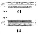
- FIGS. 1a and 1b illustrate in the schematic representation of the structure of an EL film assembly according to a first embodiment for implementing the invention:
- a PET fabric material 8 (in the example PET 1000 120-23, manufacturer Sefar, CH-Thal) with silver-coated PET fibers (here: 120 fibers / cm, 23 ⁇ m thread diameter, thickness of the silver coating about 500 nm) is coated with a transparent polymer material (Here: an acrylic resin), so that a first planar and transparent electrode layer 10 is realized.
- This electrode layer 10 can be contacted in the lateral area and has a thickness of typically between 30 ⁇ m and 200 ⁇ m. In this way, a layer is formed which is not conductive on one flat side, on its other flat side is conductive.
- This first electrode layer which in the embodiment shown permits a transmission of visible light of approximately 50%, is provided with an active layer 12 by screen printing (or other suitable coating method).
- this active layer is also carried out by a continuous process by suitable coating methods, such as blade coating, spraying, dip coating or the like.
- the active layer comprises copper-doped zinc sulfide, additionally admixed with Al 2 O 3 as another component, and prepared as a screen-printable ink / paste.
- This ink typically available commercially as product E80-02SB, manufactured by Mobichem
- E80-02SB manufactured by Mobichem
- a dielectric layer (dielectric layer 14) is applied.
- This application is carried out in two stages, wherein initially a first layer is applied by screen printing (typical paste used: type D80-01, manufacturer Mobichem, a conventional barium titanate paste, screen printing pastes used can be diluted by suitable solvents according to the coating requirements, typically a dilution of 0 to 50% takes place).
- screen printing typically paste used: type D80-01, manufacturer Mobichem, a conventional barium titanate paste, screen printing pastes used can be diluted by suitable solvents according to the coating requirements, typically a dilution of 0 to 50% takes place.
- the application is carried out so that after drying (110 ° to 130 °, 20 to 30 min.)
- This first layer has a layer thickness of about 5 to 40 microns.
- a second layer of the same dielectric material is then applied to this layer by screen printing (or another coating method), after which (again to achieve a comparable layer thickness), a silver-metallized PET fabric 16a (corresponding to the type used for the electrode layer 10) is inserted into the still undried material of the second layer, so that a (partial) penetration of the fabric material into the applied dielectric material takes place , Only then (possibly with an intermediate rolling on or pressing the fabric material for the second electrode layer 16a), the drying is carried out with heat.
- a first and a second dielectric layer are applied successively, after drying a preceding layer.
- Each dielectric layer (14) is applied by the same process conditions as described above by screen printing or other coating method so that a dried layer has an average thickness ranging between about 5 ⁇ m and 40 ⁇ m.
- a metallized layer (16b) is then applied to the (second) dielectric layer after it has dried.
- Such a metallized layer on the multilayer structure may be suitably made by plasma sputtering (for example, Ag, Au, Ti, Mo, Cr, Cu, ITO, ZAO, or the like), alternatively by deposition (Al, Ag, Cu, etc.).
- the metallization is by means of silver of a thickness in the range between 25 and 200 nm.
- the sheet resistance of this layer should preferably be relatively low, in particular ⁇ 5 ⁇ / sq.
- the first electrode layer and the second electrode layer are electrically contacted in the edge region; the FIG. 1a 1 b then illustrates the symbolic application of an alternating voltage signal for operating the device, which emits light from both electrode surfaces.
- the coating of the dielectric in two steps is preferably in (optical) Tuning with the fabric of the transparent electrode 10 is selected and aligned to avoid a (negative) moire effect. Typically, this is done by aligning the two tissues relative to each other at a predetermined angle.
- the Figure 1 b describes an additional and alternative way to implement the first embodiment wherein the second dielectric layer 14 is deposited in the same manner as the first layer.
- a metallized coating 16b is applied to the second dielectric layer after it has been dried.
- a metallic layer may suitably be made by plasma sputtering (eg, Ag, Au, Ti, Nu, Cr, Cu, ITO, ZAO or the like), alternatively by deposition (Al, Ag, Cu, etc.).
- ITO is less preferred.
- the metallization is realized from silver having a thickness in the range between 20 and 200 nm, with a sheet resistance which is relatively low at ⁇ 5 ⁇ / sq. Particles are homogeneous metal thicknesses, thus greater homogeneity of the brightness of the final product.
- An advantage of the above-described first embodiment is that relatively rough layer transitions occur. This has a positive effect on the refraction of light or the light distribution in the layer arrangement and prevents light traps.
- FIG. 2 A second embodiment of the present invention is explained, which can also be understood as an "inverted" variant, since the sequence of the layers is reversed in comparison with the previously described first exemplary embodiment. More specifically, the counter electrode is first coated with dielectric, then the active layer is applied, and then the transparent electrode is deposited.
- FIG. 2 shows FIG. 2 in the schematic arrangement of how the back electrode (counter electrode) is made of a conductive film 20 (typically a metal material metallized to achieve desired conductivity).
- This foil is thermally stabilized so that it (after drying) is stable for paste to be applied; Such thermal stabilization takes place up to temperature ranges from 130 ° C to 180 ° C.
- Foil (film) 20 is thin and flexible to realize a so-called foil back-structured lamp, typically achievable by a PET film of average thickness between 40 ⁇ m and 100 ⁇ m (preferred thickness about 50 ⁇ m).
- the appropriate metallization is in the direction of a sheet resistance typically ⁇ 50 ⁇ / sq, more preferably ⁇ 20 ⁇ / sq, even more preferably ⁇ 10 ⁇ / sq.
- a (single-layer or two-layer) dielectric layer 14 is applied thereon.
- the dielectric layer (s) are applied in the same manner as described above in connection with the first embodiment, again suitably the screen printing paste can be diluted and in the manner described above is dried.
- the active layer 12 is applied. This again corresponds to the one described above in connection with the first embodiment (corresponding screen printing paste, supplier, manufacturing and drying steps, stratification).
- a silver-metallised PET fabric 8 (corresponding to the electrode layer) is applied to this layer, into the not yet completely dried material of the last coating, so that a (partial) penetration of the fabric material with the active material takes place. Thereafter, the assembly is dried (if necessary after pressing or pressing in the second electrode layer 8, if necessary).
- the (respective) application of the coatings in an endless form so that can be made so far mass production and efficient.
- the implementation form explained above in the second embodiment is advantageous.
- a PET fabric material 8 (again, for example, PET 1000 100-23, supplier SEFAR, CH-Thal). with silver-coated PET-Fibern (here: 120 fibers / cm, 23 ⁇ m thread diameter, thickness of the silver coating about 500nm) with the active layer (direct) provided so that the fabric partially in the layer on one side and completely on the other side is embedded.
- silver-coated PET-Fibern here: 120 fibers / cm, 23 ⁇ m thread diameter, thickness of the silver coating about 500nm
- the dielectric layer is applied in the same manner as described above in connection with FIGS FIGS. 1a and 1b, in turn, the two variants are suitable for realizing the counter electrode.
- predetermining light color, brightness / permeability, mechanical strength and other parameters in particular by setting and selecting suitable tissue properties.
- fixation measures such as clamping the tissue for the second electrode layer in a frame
- fixation measures such as clamping the tissue for the second electrode layer in a frame
- the tissue properties with respect to the electrode layer 10 should be carefully determined or dimensioned, for example in order to avoid an adverse moiré effect.
- a typical procedure here is to apply the second metallized tissue at a predetermined angle with respect to the first electrode layer.
- the present invention provides in a surprisingly simple and elegant manner a variable, flexible and cost-effective to produce electroluminescent film assembly, which can potentially make EL technology accessible to a wider range of applications.
- this film arrangement can be produced endlessly ("roll-on-roll") and advantageously realize large emission surfaces with high brightness or radiation homogeneity;
- An additional advantage is the usability of comparatively high cutoff frequencies and control voltages.
Landscapes
- Physics & Mathematics (AREA)
- Electromagnetism (AREA)
- Electroluminescent Light Sources (AREA)
Applications Claiming Priority (2)
| Application Number | Priority Date | Filing Date | Title |
|---|---|---|---|
| DE102009017787A DE102009017787A1 (de) | 2009-04-20 | 2009-04-20 | Optoelektronische Folienanordnung |
| PCT/EP2010/002410 WO2010121785A1 (de) | 2009-04-20 | 2010-04-20 | Optoelektronische folienanordnung |
Publications (2)
| Publication Number | Publication Date |
|---|---|
| EP2422585A1 EP2422585A1 (de) | 2012-02-29 |
| EP2422585B1 true EP2422585B1 (de) | 2013-07-10 |
Family
ID=42312719
Family Applications (1)
| Application Number | Title | Priority Date | Filing Date |
|---|---|---|---|
| EP10718869.0A Not-in-force EP2422585B1 (de) | 2009-04-20 | 2010-04-20 | Optoelektronische folienanordnung |
Country Status (6)
| Country | Link |
|---|---|
| US (1) | US8598779B2 (enExample) |
| EP (1) | EP2422585B1 (enExample) |
| JP (1) | JP5651684B2 (enExample) |
| CN (1) | CN102405685B (enExample) |
| DE (1) | DE102009017787A1 (enExample) |
| WO (1) | WO2010121785A1 (enExample) |
Families Citing this family (10)
| Publication number | Priority date | Publication date | Assignee | Title |
|---|---|---|---|---|
| DE202011110597U1 (de) * | 2011-05-10 | 2015-03-25 | Sefar Ag | Substrat für eine optoelektronische Vorrichtung |
| FR2983771B1 (fr) * | 2011-12-09 | 2014-01-10 | Inst Francais Textile & Habillement Ifth | Textile electroluminescent et procede de fabrication d'un tel textile |
| DE202013012078U1 (de) * | 2013-02-27 | 2015-02-23 | Sefar Ag | Flächige und/oder bahnförmige Elektrolumineszenzvorrichtung |
| EP2790196A1 (de) * | 2013-04-09 | 2014-10-15 | Sefar AG | Elektrisch leitfähiges Substrat für eine optoelektrische Vorrichtung |
| DE102013019889B4 (de) * | 2013-11-28 | 2015-07-30 | Airbus Defence and Space GmbH | Photobioreaktor mit Matten aus licht-auskoppelnden Lichtleiterfasern und ein elektrisches Wanderfeld erzeugenden elektrisch leitfähigen Fasern |
| TWI602469B (zh) * | 2014-04-21 | 2017-10-11 | 財團法人紡織產業綜合研究所 | 無基材式發光元件及其製造方法 |
| EP3230078A1 (en) * | 2014-12-08 | 2017-10-18 | Gemalto AG | Flexible band |
| US10021761B2 (en) * | 2016-10-21 | 2018-07-10 | AhuraTech LLC | System and method for producing light in a liquid media |
| CN109346608B (zh) * | 2018-11-28 | 2024-03-26 | 中国华能集团有限公司 | 一种无透明电极的钙钛矿太阳能电池 |
| CN110191550B (zh) * | 2019-05-24 | 2022-05-10 | 珠海纳金科技有限公司 | 一种制作立体无机电致发光器件的方法 |
Family Cites Families (12)
| Publication number | Priority date | Publication date | Assignee | Title |
|---|---|---|---|---|
| WO1997048254A1 (en) * | 1996-06-12 | 1997-12-18 | Kue Byung Choi | Light-transmitting electroconductive plastic web electrodes and manufacturing thereof |
| JPH11224782A (ja) * | 1998-02-06 | 1999-08-17 | Kawaguchiko Seimitsu Kk | エレクトロルミネッセンス |
| US6624565B2 (en) * | 2001-07-05 | 2003-09-23 | Visson Ip, Llc | Cellular flexible display structure |
| JP2003278073A (ja) * | 2002-03-19 | 2003-10-02 | Teijin Ltd | 耐屈曲性に優れた表面導電性布帛 |
| DE10333583A1 (de) * | 2003-02-18 | 2004-09-30 | Textilforschungsinstitut Thüringen-Vogtland e.V. (TITV e.V.) | Textile Flächenstruktur aus einer Anordnung einer Vielzahl von leitfähigen oder leitfähige Eigenschaften aufweisenden Fäden sowie Verfahren zu deren Herstellung |
| EP1601741B1 (de) * | 2003-02-18 | 2008-04-16 | Textilforschungsinstitut Thüringer-Vogtland e.V. | Textile flächenstruktur aus einer anordnung einer vielzahl von leitfähigen oder leitfähige eigenschaften aufweisenden fäden sowie verfahren zu deren herstellung |
| KR20050063292A (ko) * | 2003-12-22 | 2005-06-28 | 주식회사 지에이코리아테크 | 가요성 전면전극 필름과 이를 이용한 네온 플렉스 소자 |
| EP1720380B1 (en) * | 2004-02-26 | 2016-11-02 | Toshiba Materials Co., Ltd. | Switch lighting el sheet and lighting switch and electronic apparatus using it |
| JP2006032100A (ja) * | 2004-07-15 | 2006-02-02 | Fuji Photo Film Co Ltd | 無機分散型エレクトロルミネッセンス素子 |
| JP2009076668A (ja) * | 2007-09-20 | 2009-04-09 | Dainippon Printing Co Ltd | 有機薄膜太陽電池 |
| JP5212377B2 (ja) | 2007-11-07 | 2013-06-19 | コニカミノルタホールディングス株式会社 | 透明電極及び透明電極の製造方法 |
| DE102008055969A1 (de) | 2008-11-05 | 2010-06-10 | Sefar Ag | Substrat für eine optoelektronische Vorrichtung |
-
2009
- 2009-04-20 DE DE102009017787A patent/DE102009017787A1/de not_active Withdrawn
-
2010
- 2010-04-20 JP JP2012506386A patent/JP5651684B2/ja not_active Expired - Fee Related
- 2010-04-20 CN CN201080017243.6A patent/CN102405685B/zh not_active Expired - Fee Related
- 2010-04-20 EP EP10718869.0A patent/EP2422585B1/de not_active Not-in-force
- 2010-04-20 US US13/265,018 patent/US8598779B2/en not_active Expired - Fee Related
- 2010-04-20 WO PCT/EP2010/002410 patent/WO2010121785A1/de not_active Ceased
Also Published As
| Publication number | Publication date |
|---|---|
| JP2012524384A (ja) | 2012-10-11 |
| EP2422585A1 (de) | 2012-02-29 |
| CN102405685A (zh) | 2012-04-04 |
| US8598779B2 (en) | 2013-12-03 |
| JP5651684B2 (ja) | 2015-01-14 |
| WO2010121785A1 (de) | 2010-10-28 |
| CN102405685B (zh) | 2015-11-25 |
| US20120043879A1 (en) | 2012-02-23 |
| DE102009017787A1 (de) | 2010-10-28 |
Similar Documents
| Publication | Publication Date | Title |
|---|---|---|
| EP2422585B1 (de) | Optoelektronische folienanordnung | |
| EP2347449B1 (de) | Substrat für eine optoelektronische vorrichtung | |
| EP2126998B1 (de) | Oled mit farbkonversion | |
| EP2694712B1 (de) | Elektrodensubstrat sowie flächige optoelektronische vorrichtung | |
| EP2002493B1 (de) | Grossflächige oled's mit homogener lichtemission | |
| DE102018118116B4 (de) | Verfahren zur Herstellung eines elektrisch leitfähigen Substrats und einer Anzeigevorrichtung | |
| DE102007030108A1 (de) | Anorganisches Dickfilm-AC Elektrolumineszenzelement mit zumindest zwei Einspeisungen und Herstellverfahren und Anwendung | |
| EP2294642A1 (de) | Verfahren zur herstellung eines organischen elektronischen bauelements und organisches elektronisches bauelement | |
| EP2790196A1 (de) | Elektrisch leitfähiges Substrat für eine optoelektrische Vorrichtung | |
| EP2395572A1 (de) | Schichtaufbau umfassend elektrotechnische Bauelemente | |
| DE10228939A1 (de) | Elektrolumineszierende Vorrichtung mit transparenter Kathode | |
| DE102013107675A1 (de) | Bauteil und Verfahren zum Betrieb eines Bauteils | |
| WO2018060258A1 (de) | Kontaktierung von optoelektronischen bauelementen | |
| EP1638155A1 (de) | Verbesserung der Leitfähigkeit einer Polymerelektrode durch Aufbringen einer darunterliegenden Metallschicht | |
| DE102008039756A1 (de) | Beleuchtungselement und Verfahren zu seiner Herstellung | |
| DE102017117051B4 (de) | Organisches Licht emittierendes Bauelement und Licht emittierende Vorrichtung | |
| WO2016146438A1 (de) | Verfahren zum herstellen eines optoelektronischen bauelements | |
| WO1998054767A1 (de) | Leitfähiges schichtsystem und dessen verwendung in elektrolumineszierenden anordnungen | |
| DE102008021655B4 (de) | Strahlungsquelle und Solarzelle | |
| DE202011110597U1 (de) | Substrat für eine optoelektronische Vorrichtung | |
| EP2119319A1 (de) | Elektrolumineszenzleuchte und verfahren zu ihrer herstellung | |
| WO2008083671A1 (de) | Optoelektronische vorrichtung und verfahren zur herstellung einer optoelektronischen vorrichtung | |
| EP2130408A1 (de) | Elektrolumineszierendes schichtelement | |
| WO2016156026A1 (de) | Organische leuchtdiode und verfahren zur herstellung einer organischen leuchtdiode | |
| EP1983593A2 (de) | Organisches optoelektronisches Bauelement |
Legal Events
| Date | Code | Title | Description |
|---|---|---|---|
| PUAI | Public reference made under article 153(3) epc to a published international application that has entered the european phase |
Free format text: ORIGINAL CODE: 0009012 |
|
| 17P | Request for examination filed |
Effective date: 20111117 |
|
| AK | Designated contracting states |
Kind code of ref document: A1 Designated state(s): AT BE BG CH CY CZ DE DK EE ES FI FR GB GR HR HU IE IS IT LI LT LU LV MC MK MT NL NO PL PT RO SE SI SK SM TR |
|
| REG | Reference to a national code |
Ref country code: DE Ref legal event code: R079 Ref document number: 502010003963 Country of ref document: DE Free format text: PREVIOUS MAIN CLASS: H05B0033140000 Ipc: H01L0051440000 |
|
| DAX | Request for extension of the european patent (deleted) | ||
| RIC1 | Information provided on ipc code assigned before grant |
Ipc: H01L 51/44 20060101AFI20120807BHEP Ipc: H05B 33/14 20060101ALI20120807BHEP Ipc: H05B 33/28 20060101ALI20120807BHEP |
|
| GRAP | Despatch of communication of intention to grant a patent |
Free format text: ORIGINAL CODE: EPIDOSNIGR1 |
|
| GRAJ | Information related to disapproval of communication of intention to grant by the applicant or resumption of examination proceedings by the epo deleted |
Free format text: ORIGINAL CODE: EPIDOSDIGR1 |
|
| GRAP | Despatch of communication of intention to grant a patent |
Free format text: ORIGINAL CODE: EPIDOSNIGR1 |
|
| GRAS | Grant fee paid |
Free format text: ORIGINAL CODE: EPIDOSNIGR3 |
|
| GRAA | (expected) grant |
Free format text: ORIGINAL CODE: 0009210 |
|
| AK | Designated contracting states |
Kind code of ref document: B1 Designated state(s): AT BE BG CH CY CZ DE DK EE ES FI FR GB GR HR HU IE IS IT LI LT LU LV MC MK MT NL NO PL PT RO SE SI SK SM TR |
|
| REG | Reference to a national code |
Ref country code: GB Ref legal event code: FG4D Free format text: NOT ENGLISH |
|
| REG | Reference to a national code |
Ref country code: CH Ref legal event code: EP Ref country code: AT Ref legal event code: REF Ref document number: 621398 Country of ref document: AT Kind code of ref document: T Effective date: 20130715 |
|
| REG | Reference to a national code |
Ref country code: IE Ref legal event code: FG4D Free format text: LANGUAGE OF EP DOCUMENT: GERMAN |
|
| REG | Reference to a national code |
Ref country code: DE Ref legal event code: R096 Ref document number: 502010003963 Country of ref document: DE Effective date: 20130905 |
|
| PG25 | Lapsed in a contracting state [announced via postgrant information from national office to epo] |
Ref country code: SI Free format text: LAPSE BECAUSE OF FAILURE TO SUBMIT A TRANSLATION OF THE DESCRIPTION OR TO PAY THE FEE WITHIN THE PRESCRIBED TIME-LIMIT Effective date: 20130710 |
|
| REG | Reference to a national code |
Ref country code: CH Ref legal event code: NV Representative=s name: BODENSEEPATENT GMBH, CH |
|
| REG | Reference to a national code |
Ref country code: NL Ref legal event code: VDEP Effective date: 20130710 |
|
| REG | Reference to a national code |
Ref country code: LT Ref legal event code: MG4D |
|
| PG25 | Lapsed in a contracting state [announced via postgrant information from national office to epo] |
Ref country code: CY Free format text: LAPSE BECAUSE OF FAILURE TO SUBMIT A TRANSLATION OF THE DESCRIPTION OR TO PAY THE FEE WITHIN THE PRESCRIBED TIME-LIMIT Effective date: 20130814 Ref country code: NO Free format text: LAPSE BECAUSE OF FAILURE TO SUBMIT A TRANSLATION OF THE DESCRIPTION OR TO PAY THE FEE WITHIN THE PRESCRIBED TIME-LIMIT Effective date: 20131010 Ref country code: IS Free format text: LAPSE BECAUSE OF FAILURE TO SUBMIT A TRANSLATION OF THE DESCRIPTION OR TO PAY THE FEE WITHIN THE PRESCRIBED TIME-LIMIT Effective date: 20131110 Ref country code: SE Free format text: LAPSE BECAUSE OF FAILURE TO SUBMIT A TRANSLATION OF THE DESCRIPTION OR TO PAY THE FEE WITHIN THE PRESCRIBED TIME-LIMIT Effective date: 20130710 Ref country code: PT Free format text: LAPSE BECAUSE OF FAILURE TO SUBMIT A TRANSLATION OF THE DESCRIPTION OR TO PAY THE FEE WITHIN THE PRESCRIBED TIME-LIMIT Effective date: 20131111 Ref country code: LT Free format text: LAPSE BECAUSE OF FAILURE TO SUBMIT A TRANSLATION OF THE DESCRIPTION OR TO PAY THE FEE WITHIN THE PRESCRIBED TIME-LIMIT Effective date: 20130710 Ref country code: HR Free format text: LAPSE BECAUSE OF FAILURE TO SUBMIT A TRANSLATION OF THE DESCRIPTION OR TO PAY THE FEE WITHIN THE PRESCRIBED TIME-LIMIT Effective date: 20130710 |
|
| PG25 | Lapsed in a contracting state [announced via postgrant information from national office to epo] |
Ref country code: NL Free format text: LAPSE BECAUSE OF FAILURE TO SUBMIT A TRANSLATION OF THE DESCRIPTION OR TO PAY THE FEE WITHIN THE PRESCRIBED TIME-LIMIT Effective date: 20130710 Ref country code: ES Free format text: LAPSE BECAUSE OF FAILURE TO SUBMIT A TRANSLATION OF THE DESCRIPTION OR TO PAY THE FEE WITHIN THE PRESCRIBED TIME-LIMIT Effective date: 20131021 Ref country code: LV Free format text: LAPSE BECAUSE OF FAILURE TO SUBMIT A TRANSLATION OF THE DESCRIPTION OR TO PAY THE FEE WITHIN THE PRESCRIBED TIME-LIMIT Effective date: 20130710 Ref country code: FI Free format text: LAPSE BECAUSE OF FAILURE TO SUBMIT A TRANSLATION OF THE DESCRIPTION OR TO PAY THE FEE WITHIN THE PRESCRIBED TIME-LIMIT Effective date: 20130710 Ref country code: GR Free format text: LAPSE BECAUSE OF FAILURE TO SUBMIT A TRANSLATION OF THE DESCRIPTION OR TO PAY THE FEE WITHIN THE PRESCRIBED TIME-LIMIT Effective date: 20131011 Ref country code: PL Free format text: LAPSE BECAUSE OF FAILURE TO SUBMIT A TRANSLATION OF THE DESCRIPTION OR TO PAY THE FEE WITHIN THE PRESCRIBED TIME-LIMIT Effective date: 20130710 |
|
| PG25 | Lapsed in a contracting state [announced via postgrant information from national office to epo] |
Ref country code: CY Free format text: LAPSE BECAUSE OF FAILURE TO SUBMIT A TRANSLATION OF THE DESCRIPTION OR TO PAY THE FEE WITHIN THE PRESCRIBED TIME-LIMIT Effective date: 20130710 |
|
| PG25 | Lapsed in a contracting state [announced via postgrant information from national office to epo] |
Ref country code: EE Free format text: LAPSE BECAUSE OF FAILURE TO SUBMIT A TRANSLATION OF THE DESCRIPTION OR TO PAY THE FEE WITHIN THE PRESCRIBED TIME-LIMIT Effective date: 20130710 Ref country code: RO Free format text: LAPSE BECAUSE OF FAILURE TO SUBMIT A TRANSLATION OF THE DESCRIPTION OR TO PAY THE FEE WITHIN THE PRESCRIBED TIME-LIMIT Effective date: 20130710 Ref country code: SK Free format text: LAPSE BECAUSE OF FAILURE TO SUBMIT A TRANSLATION OF THE DESCRIPTION OR TO PAY THE FEE WITHIN THE PRESCRIBED TIME-LIMIT Effective date: 20130710 Ref country code: DK Free format text: LAPSE BECAUSE OF FAILURE TO SUBMIT A TRANSLATION OF THE DESCRIPTION OR TO PAY THE FEE WITHIN THE PRESCRIBED TIME-LIMIT Effective date: 20130710 Ref country code: CZ Free format text: LAPSE BECAUSE OF FAILURE TO SUBMIT A TRANSLATION OF THE DESCRIPTION OR TO PAY THE FEE WITHIN THE PRESCRIBED TIME-LIMIT Effective date: 20130710 |
|
| PLBE | No opposition filed within time limit |
Free format text: ORIGINAL CODE: 0009261 |
|
| STAA | Information on the status of an ep patent application or granted ep patent |
Free format text: STATUS: NO OPPOSITION FILED WITHIN TIME LIMIT |
|
| PG25 | Lapsed in a contracting state [announced via postgrant information from national office to epo] |
Ref country code: IT Free format text: LAPSE BECAUSE OF FAILURE TO SUBMIT A TRANSLATION OF THE DESCRIPTION OR TO PAY THE FEE WITHIN THE PRESCRIBED TIME-LIMIT Effective date: 20130710 |
|
| 26N | No opposition filed |
Effective date: 20140411 |
|
| REG | Reference to a national code |
Ref country code: DE Ref legal event code: R097 Ref document number: 502010003963 Country of ref document: DE Effective date: 20140411 |
|
| PGFP | Annual fee paid to national office [announced via postgrant information from national office to epo] |
Ref country code: IE Payment date: 20140416 Year of fee payment: 5 |
|
| PGFP | Annual fee paid to national office [announced via postgrant information from national office to epo] |
Ref country code: TR Payment date: 20140411 Year of fee payment: 5 |
|
| PG25 | Lapsed in a contracting state [announced via postgrant information from national office to epo] |
Ref country code: LU Free format text: LAPSE BECAUSE OF FAILURE TO SUBMIT A TRANSLATION OF THE DESCRIPTION OR TO PAY THE FEE WITHIN THE PRESCRIBED TIME-LIMIT Effective date: 20140420 Ref country code: MC Free format text: LAPSE BECAUSE OF FAILURE TO SUBMIT A TRANSLATION OF THE DESCRIPTION OR TO PAY THE FEE WITHIN THE PRESCRIBED TIME-LIMIT Effective date: 20130710 |
|
| REG | Reference to a national code |
Ref country code: IE Ref legal event code: MM4A |
|
| PG25 | Lapsed in a contracting state [announced via postgrant information from national office to epo] |
Ref country code: MT Free format text: LAPSE BECAUSE OF FAILURE TO SUBMIT A TRANSLATION OF THE DESCRIPTION OR TO PAY THE FEE WITHIN THE PRESCRIBED TIME-LIMIT Effective date: 20130710 |
|
| REG | Reference to a national code |
Ref country code: FR Ref legal event code: PLFP Year of fee payment: 7 |
|
| PG25 | Lapsed in a contracting state [announced via postgrant information from national office to epo] |
Ref country code: IE Free format text: LAPSE BECAUSE OF NON-PAYMENT OF DUE FEES Effective date: 20150420 Ref country code: SM Free format text: LAPSE BECAUSE OF FAILURE TO SUBMIT A TRANSLATION OF THE DESCRIPTION OR TO PAY THE FEE WITHIN THE PRESCRIBED TIME-LIMIT Effective date: 20130710 |
|
| REG | Reference to a national code |
Ref country code: AT Ref legal event code: MM01 Ref document number: 621398 Country of ref document: AT Kind code of ref document: T Effective date: 20150420 |
|
| PG25 | Lapsed in a contracting state [announced via postgrant information from national office to epo] |
Ref country code: BG Free format text: LAPSE BECAUSE OF FAILURE TO SUBMIT A TRANSLATION OF THE DESCRIPTION OR TO PAY THE FEE WITHIN THE PRESCRIBED TIME-LIMIT Effective date: 20130710 |
|
| PG25 | Lapsed in a contracting state [announced via postgrant information from national office to epo] |
Ref country code: HU Free format text: LAPSE BECAUSE OF FAILURE TO SUBMIT A TRANSLATION OF THE DESCRIPTION OR TO PAY THE FEE WITHIN THE PRESCRIBED TIME-LIMIT; INVALID AB INITIO Effective date: 20100420 Ref country code: BE Free format text: LAPSE BECAUSE OF FAILURE TO SUBMIT A TRANSLATION OF THE DESCRIPTION OR TO PAY THE FEE WITHIN THE PRESCRIBED TIME-LIMIT Effective date: 20140430 |
|
| PG25 | Lapsed in a contracting state [announced via postgrant information from national office to epo] |
Ref country code: AT Free format text: LAPSE BECAUSE OF NON-PAYMENT OF DUE FEES Effective date: 20150420 |
|
| REG | Reference to a national code |
Ref country code: FR Ref legal event code: PLFP Year of fee payment: 8 |
|
| PG25 | Lapsed in a contracting state [announced via postgrant information from national office to epo] |
Ref country code: TR Free format text: LAPSE BECAUSE OF NON-PAYMENT OF DUE FEES Effective date: 20150420 |
|
| REG | Reference to a national code |
Ref country code: FR Ref legal event code: PLFP Year of fee payment: 9 |
|
| PG25 | Lapsed in a contracting state [announced via postgrant information from national office to epo] |
Ref country code: MK Free format text: LAPSE BECAUSE OF FAILURE TO SUBMIT A TRANSLATION OF THE DESCRIPTION OR TO PAY THE FEE WITHIN THE PRESCRIBED TIME-LIMIT Effective date: 20130710 |
|
| PGFP | Annual fee paid to national office [announced via postgrant information from national office to epo] |
Ref country code: DE Payment date: 20180424 Year of fee payment: 9 Ref country code: CH Payment date: 20180424 Year of fee payment: 9 |
|
| PGFP | Annual fee paid to national office [announced via postgrant information from national office to epo] |
Ref country code: FR Payment date: 20180424 Year of fee payment: 9 |
|
| PGFP | Annual fee paid to national office [announced via postgrant information from national office to epo] |
Ref country code: GB Payment date: 20180424 Year of fee payment: 9 |
|
| REG | Reference to a national code |
Ref country code: DE Ref legal event code: R119 Ref document number: 502010003963 Country of ref document: DE |
|
| REG | Reference to a national code |
Ref country code: CH Ref legal event code: PL |
|
| GBPC | Gb: european patent ceased through non-payment of renewal fee |
Effective date: 20190420 |
|
| PG25 | Lapsed in a contracting state [announced via postgrant information from national office to epo] |
Ref country code: LI Free format text: LAPSE BECAUSE OF NON-PAYMENT OF DUE FEES Effective date: 20190430 Ref country code: DE Free format text: LAPSE BECAUSE OF NON-PAYMENT OF DUE FEES Effective date: 20191101 Ref country code: CH Free format text: LAPSE BECAUSE OF NON-PAYMENT OF DUE FEES Effective date: 20190430 Ref country code: GB Free format text: LAPSE BECAUSE OF NON-PAYMENT OF DUE FEES Effective date: 20190420 |
|
| PG25 | Lapsed in a contracting state [announced via postgrant information from national office to epo] |
Ref country code: FR Free format text: LAPSE BECAUSE OF NON-PAYMENT OF DUE FEES Effective date: 20190430 |