EP2417526B1 - System and method for ensuring consistency between a data cache and a main memory - Google Patents
System and method for ensuring consistency between a data cache and a main memory Download PDFInfo
- Publication number
- EP2417526B1 EP2417526B1 EP10723271.2A EP10723271A EP2417526B1 EP 2417526 B1 EP2417526 B1 EP 2417526B1 EP 10723271 A EP10723271 A EP 10723271A EP 2417526 B1 EP2417526 B1 EP 2417526B1
- Authority
- EP
- European Patent Office
- Prior art keywords
- memory
- thread
- request
- address
- barrier
- Prior art date
- Legal status (The legal status is an assumption and is not a legal conclusion. Google has not performed a legal analysis and makes no representation as to the accuracy of the status listed.)
- Active
Links
Images


Classifications
-
- G—PHYSICS
- G06—COMPUTING OR CALCULATING; COUNTING
- G06F—ELECTRIC DIGITAL DATA PROCESSING
- G06F12/00—Accessing, addressing or allocating within memory systems or architectures
- G06F12/02—Addressing or allocation; Relocation
- G06F12/08—Addressing or allocation; Relocation in hierarchically structured memory systems, e.g. virtual memory systems
- G06F12/0802—Addressing of a memory level in which the access to the desired data or data block requires associative addressing means, e.g. caches
- G06F12/0806—Multiuser, multiprocessor or multiprocessing cache systems
- G06F12/0815—Cache consistency protocols
-
- G—PHYSICS
- G06—COMPUTING OR CALCULATING; COUNTING
- G06F—ELECTRIC DIGITAL DATA PROCESSING
- G06F9/00—Arrangements for program control, e.g. control units
- G06F9/06—Arrangements for program control, e.g. control units using stored programs, i.e. using an internal store of processing equipment to receive or retain programs
- G06F9/30—Arrangements for executing machine instructions, e.g. instruction decode
- G06F9/38—Concurrent instruction execution, e.g. pipeline or look ahead
- G06F9/3824—Operand accessing
- G06F9/3834—Maintaining memory consistency
-
- G—PHYSICS
- G06—COMPUTING OR CALCULATING; COUNTING
- G06F—ELECTRIC DIGITAL DATA PROCESSING
- G06F12/00—Accessing, addressing or allocating within memory systems or architectures
- G06F12/02—Addressing or allocation; Relocation
- G06F12/08—Addressing or allocation; Relocation in hierarchically structured memory systems, e.g. virtual memory systems
- G06F12/0802—Addressing of a memory level in which the access to the desired data or data block requires associative addressing means, e.g. caches
- G06F12/0844—Multiple simultaneous or quasi-simultaneous cache accessing
- G06F12/0855—Overlapped cache accessing, e.g. pipeline
- G06F12/0859—Overlapped cache accessing, e.g. pipeline with reload from main memory
-
- G—PHYSICS
- G06—COMPUTING OR CALCULATING; COUNTING
- G06F—ELECTRIC DIGITAL DATA PROCESSING
- G06F12/00—Accessing, addressing or allocating within memory systems or architectures
- G06F12/02—Addressing or allocation; Relocation
- G06F12/08—Addressing or allocation; Relocation in hierarchically structured memory systems, e.g. virtual memory systems
- G06F12/0802—Addressing of a memory level in which the access to the desired data or data block requires associative addressing means, e.g. caches
- G06F12/0806—Multiuser, multiprocessor or multiprocessing cache systems
- G06F12/0815—Cache consistency protocols
- G06F12/0817—Cache consistency protocols using directory methods
- G06F12/0828—Cache consistency protocols using directory methods with concurrent directory accessing, i.e. handling multiple concurrent coherency transactions
-
- G—PHYSICS
- G06—COMPUTING OR CALCULATING; COUNTING
- G06F—ELECTRIC DIGITAL DATA PROCESSING
- G06F12/00—Accessing, addressing or allocating within memory systems or architectures
- G06F12/02—Addressing or allocation; Relocation
- G06F12/08—Addressing or allocation; Relocation in hierarchically structured memory systems, e.g. virtual memory systems
- G06F12/0802—Addressing of a memory level in which the access to the desired data or data block requires associative addressing means, e.g. caches
- G06F12/0875—Addressing of a memory level in which the access to the desired data or data block requires associative addressing means, e.g. caches with dedicated cache, e.g. instruction or stack
-
- G—PHYSICS
- G06—COMPUTING OR CALCULATING; COUNTING
- G06F—ELECTRIC DIGITAL DATA PROCESSING
- G06F8/00—Arrangements for software engineering
- G06F8/40—Transformation of program code
- G06F8/41—Compilation
- G06F8/45—Exploiting coarse grain parallelism in compilation, i.e. parallelism between groups of instructions
- G06F8/458—Synchronisation, e.g. post-wait, barriers, locks
-
- G—PHYSICS
- G06—COMPUTING OR CALCULATING; COUNTING
- G06F—ELECTRIC DIGITAL DATA PROCESSING
- G06F9/00—Arrangements for program control, e.g. control units
- G06F9/06—Arrangements for program control, e.g. control units using stored programs, i.e. using an internal store of processing equipment to receive or retain programs
- G06F9/30—Arrangements for executing machine instructions, e.g. instruction decode
- G06F9/38—Concurrent instruction execution, e.g. pipeline or look ahead
- G06F9/3836—Instruction issuing, e.g. dynamic instruction scheduling or out of order instruction execution
- G06F9/3851—Instruction issuing, e.g. dynamic instruction scheduling or out of order instruction execution from multiple instruction streams, e.g. multistreaming
-
- G—PHYSICS
- G06—COMPUTING OR CALCULATING; COUNTING
- G06F—ELECTRIC DIGITAL DATA PROCESSING
- G06F12/00—Accessing, addressing or allocating within memory systems or architectures
- G06F12/02—Addressing or allocation; Relocation
- G06F12/08—Addressing or allocation; Relocation in hierarchically structured memory systems, e.g. virtual memory systems
- G06F12/0802—Addressing of a memory level in which the access to the desired data or data block requires associative addressing means, e.g. caches
- G06F12/0806—Multiuser, multiprocessor or multiprocessing cache systems
- G06F12/0842—Multiuser, multiprocessor or multiprocessing cache systems for multiprocessing or multitasking
-
- G—PHYSICS
- G06—COMPUTING OR CALCULATING; COUNTING
- G06F—ELECTRIC DIGITAL DATA PROCESSING
- G06F2212/00—Indexing scheme relating to accessing, addressing or allocation within memory systems or architectures
- G06F2212/45—Caching of specific data in cache memory
- G06F2212/452—Instruction code
-
- G—PHYSICS
- G06—COMPUTING OR CALCULATING; COUNTING
- G06F—ELECTRIC DIGITAL DATA PROCESSING
- G06F2212/00—Indexing scheme relating to accessing, addressing or allocation within memory systems or architectures
- G06F2212/62—Details of cache specific to multiprocessor cache arrangements
- G06F2212/621—Coherency control relating to peripheral accessing, e.g. from DMA or I/O device
-
- G—PHYSICS
- G06—COMPUTING OR CALCULATING; COUNTING
- G06F—ELECTRIC DIGITAL DATA PROCESSING
- G06F8/00—Arrangements for software engineering
- G06F8/40—Transformation of program code
- G06F8/41—Compilation
- G06F8/43—Checking; Contextual analysis
- G06F8/433—Dependency analysis; Data or control flow analysis
-
- G—PHYSICS
- G06—COMPUTING OR CALCULATING; COUNTING
- G06F—ELECTRIC DIGITAL DATA PROCESSING
- G06F9/00—Arrangements for program control, e.g. control units
- G06F9/06—Arrangements for program control, e.g. control units using stored programs, i.e. using an internal store of processing equipment to receive or retain programs
- G06F9/46—Multiprogramming arrangements
- G06F9/52—Program synchronisation; Mutual exclusion, e.g. by means of semaphores
- G06F9/522—Barrier synchronisation
Definitions
- the invention relates to multi-threaded processors, and in particular to the problem of data incoherency between a cache memory accessed by multiple threads and the main memory in a multi-threaded processor.
- a multi-threaded processor is capable of processing multiple different instruction sequences (or threads) simultaneously.
- execution of a thread data and instructions need to be accessed from memory. Different threads may therefore need to access memory, and sometimes the same portion of memory, simultaneously. There therefore needs to be some arbitration between threads for memory access.
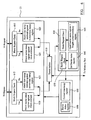
- a multi-threaded processor typically has an instruction cache and a data cache containing the most commonly accessed data and instructions, as shown in Figure 1 . If the required data or instructions are not found in the caches then access to the memory on the memory bus must be requested. Access to the memory has to be controlled to ensure threads do not conflict with each other. For this reason, memory accesses from different threads from the instruction and data caches each have their own dedicated data path up to the memory arbiter module.
- FIG. 1 is a schematic illustration of a memory access system in a multi-threaded processor in accordance with the prior art.
- Threads running on the processor core 10 can request data and instructions from the data and instruction caches 11, 12.
- the instruction and data caches each have memory management units associated with them. If the requested data or instructions are not in one of the caches, the request is passed to the memory bus.
- the requests are routed first through a thread arbiter 13, 14, which orders the requests for that thread, and then a memory arbiter 15, which controls access to the memory bus.
- cache lines Within the main memory, data is typically stored and accessible in units of a fixed number of bits, called cache lines. So, in order to read a memory address from the memory, the entire cache line containing that address must be fetched. There are two types of cache line. One type is a local cache line that only stores data for a particular thread. The other is a global cache line that stores data accessible by different threads. Whether a piece of data is stored within a global or local cache line depends on its linear address. The present invention is concerned with memory resources that are shared between threads, i.e. global cache lines.
- a global cache line might store the values of software local variables entered by different threads in different word positions within the cache line. It is expected that when a thread Tx reads its local variable from the cache line it would get back its last written value. However, situations can arise when using write through data caches in which accesses by the other threads to their local variables within the same cache line cause the thread Tx to read an old and wrong value. When this happens Tx is said to have become "data incoherent".
- Figure 2a and 2b each illustrate an example sequence of accesses by different threads causing data incoherence on thread T0.
- T0 first accesses its local variable, A, with a write request.
- T1 then accesses its local variable, B, with a read request.
- the physical addresses of A and B are such that they are cached within the same global data cache line. Initially both A and B are not in the cache.
- Read requests typically take less time to reach the memory bus than write requests.
- the T1 read reaches the memory before the T0 write.
- an old value of the cache line is stored in the data cache.
- the T0 write request does not write to the data cache, only to the memory bus. So, subsequent reads of the cache line from the data cache will fetch the old values that are stored in the data cache as a result of the T1 read.
- This invention aims to address this problem by detecting the incoherency hazard and using a mechanism to ensure that read or write instructions are only issued out of the memory bus when it is safe to.do so.
- US 6 360 298 B1 (Osanai et al ) describes a control circuit for detecting a load and a store miss to the same cache line in a pipelined processor where the store is to a write-through no-allocate memory area.
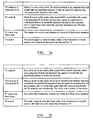
- Figures 4e and 4f illustrate the addition of two more write request addresses, 0x80000000 and 0x90000000 which cannot be compacted into existing slots. After the addition of these addresses, all the slots are being used.
- Figure 5 shows the component parts of the incoherency detection module of Figure 3 .
- the incoherency detection module Upon receiving a request from thread Tx the incoherency detection module first determines at block 500 if it is a read request or a write request to a global cache line.
- the read request address does not fall within an address range in the GWAM of another thread, then the read request can be passed to the memory arbiter without the insertion of any barrier flags or barrier requests.
- the barrier is inserted as a new barrier request. This is indicated at block 565.
- sideband data referred to as block check data
- a time stamp which is appended to each request is incremented or toggled.
- the block check data includes the thread ID of every matching thread for which barriers have been inserted.
- the requests are then queued in the per-thread FIFOs 580 until they can be issued to the memory arbiter.
- time-stamp is used herein to mean a piece of data related to time, which, when changed, marks a new time period. In a preferred embodiment, the time stamp is a one-bit field that can take on a value of 0 or 1.
- the read and write requests for each thread are queued in per thread request FIFOs 580.
- a multiplex function 570 is shown in Figure 5 to illustrate that the requests and barriers are routed to the appropriate thread FIFO 580.
- the arrow from block 565 indicates a barrier request for insertion.
- the arrow from the top of the Figure indicated the read and write requests that are added into the per-thread FIFOs via the multiplexer 570. So, if a barrier is to be inserted as a separate barrier request it is queued in the correct thread request FIFO, while the corresponding read request is queued in its thread request FIFO.
- a barrier either as sideband data or as a separate barrier request, is included in a request queue
- the GWAM for that thread is flushed. All entries in the GWAM can be erased as there is no longer any incoherency hazard associated with those memory address entries.
- a request arriving from the incoherency detection module is a global read request with block check sideband data. If it is a global read request with block check sideband data, at block 620 the memory arbiter reads the barrier data in the block check sideband data and checks it against the barrier status register to determine if the associated barriers have all been issued by the thread arbiter 610. If all the associated barriers have been issued, the global read request is released to the thread arbiter. If not all associated barriers have been issued by the thread arbiter, the global read request is blocked at the input of the memory arbiter. These checks are repeated until the global read request can be released.
- the barrier status register and time stamp register are updated as described above and illustrated in Figure 6 .
- the requests are checked for global read requests with block check sideband data and for barriers at block 630 and 635. If a barrier is detected the barrier status register is updated at block 640. If a global read request with block check sideband data is detected, the barrier status register is cleared and the internal timestamp in the timestamp register is toggled at block 645.
- the memory arbiter decodes those order enforcement sideband values and takes the appropriate action:
- the incoherency hazard illustrated in Figure 2b can be addressed using a different mechanism.
- the data cache contains a TAG RAM storing the physical addresses of the cache lines in the DATA RAM of the data cache.
- TAG RAM storing the physical addresses of the cache lines in the DATA RAM of the data cache.
- an entry from the TAG RAM is chosen to store the physical address information of the cache line to be fetched by the read request.
- a filling flag can be added to this physical address information in the TAG RAM, which indicates that that portion of the RAM has been set aside for the cache line currently being fetched.
- the filling flag takes the value 1 when the cache line is being fetched and 0 when there is no cache line being fetched.
- the filling flag has a value 1
- another flag in the TAG RAM is set for that cache line, referred to as the "dirty flag".
- the dirty flag has a value 1 it indicates that there is a potential incoherency hazard because one thread is modifying the cache line that is currently being fetched, and so there is no guarantee that the data eventually put in the data cache will be the most up-to-date data.
- the dirty flag is 1, the cache line is considered invalid as its data cannot be trusted. In this case, subsequent read requests will ignore the data in the data cache and will fetch the up-to-date data from the main memory.
- T0 read A Although the Tag RAM content indicates a cache hit, because the data cache contains cache line including A, the dirty flag is set to 1 for that cache line. The hardware then decides that this read misses in the cache, and the line is fetched again from the memory bus. Since this read occurs after the T0 write, the read returns the latest value of A and data coherency is maintained.
Landscapes
- Engineering & Computer Science (AREA)
- Theoretical Computer Science (AREA)
- General Engineering & Computer Science (AREA)
- Physics & Mathematics (AREA)
- General Physics & Mathematics (AREA)
- Software Systems (AREA)
- Multimedia (AREA)
- Memory System Of A Hierarchy Structure (AREA)
Applications Claiming Priority (2)
| Application Number | Priority Date | Filing Date | Title |
|---|---|---|---|
| GB0906066A GB2469299B (en) | 2009-04-07 | 2009-04-07 | Ensuring consistency between a data cache and a main memory |
| PCT/GB2010/000727 WO2010116151A1 (en) | 2009-04-07 | 2010-04-07 | Ensuring consistency between a data cache and a main memory |
Publications (2)
| Publication Number | Publication Date |
|---|---|
| EP2417526A1 EP2417526A1 (en) | 2012-02-15 |
| EP2417526B1 true EP2417526B1 (en) | 2013-10-16 |
Family
ID=40750290
Family Applications (1)
| Application Number | Title | Priority Date | Filing Date |
|---|---|---|---|
| EP10723271.2A Active EP2417526B1 (en) | 2009-04-07 | 2010-04-07 | System and method for ensuring consistency between a data cache and a main memory |
Country Status (6)
| Country | Link |
|---|---|
| US (3) | US8234455B2 (enExample) |
| EP (1) | EP2417526B1 (enExample) |
| JP (1) | JP5619869B2 (enExample) |
| CN (1) | CN102388372B (enExample) |
| GB (1) | GB2469299B (enExample) |
| WO (1) | WO2010116151A1 (enExample) |
Families Citing this family (22)
| Publication number | Priority date | Publication date | Assignee | Title |
|---|---|---|---|---|
| US20120290780A1 (en) * | 2011-01-27 | 2012-11-15 | Mips Technologies Inc. | Multithreaded Operation of A Microprocessor Cache |
| US8812621B2 (en) * | 2011-05-03 | 2014-08-19 | Cisco Technology, Inc. | Reducing fetching load on cache servers in adaptive streaming |
| US9195596B2 (en) * | 2011-11-02 | 2015-11-24 | Avago Technologies General Ip (Singapore) Pte. Ltd. | Mapping of valid and dirty flags in a caching system |
| CN103543954B (zh) * | 2012-07-16 | 2018-03-23 | 深圳市中兴微电子技术有限公司 | 一种数据存储管理方法和装置 |
| US9483325B2 (en) | 2012-09-28 | 2016-11-01 | Hewlett Packard Enterprise Development Lp | Synchronizing timestamp counters |
| CN105453055B (zh) * | 2012-10-25 | 2018-09-21 | 英派尔科技开发有限公司 | 晶片、维持多核处理器一致性和处理特定块请求的方法 |
| US9146678B2 (en) * | 2013-04-29 | 2015-09-29 | International Business Machines Corporation | High throughput hardware acceleration using pre-staging buffers |
| US9563561B2 (en) * | 2013-06-25 | 2017-02-07 | Intel Corporation | Initiation of cache flushes and invalidations on graphics processors |
| KR101968501B1 (ko) * | 2014-05-29 | 2019-04-15 | 삼성에스디에스 주식회사 | 데이터 처리 장치 및 데이터 처리 장치의 메모리에 기록된 데이터의 확인 방법 |
| GB2542214B (en) * | 2015-11-11 | 2019-08-28 | Imagination Tech Ltd | Hardware monitor to verify memory units |
| CN105357305B (zh) * | 2015-11-13 | 2018-11-20 | 北京金山安全软件有限公司 | 文件发送方法和装置、文件接收方法和装置和终端设备 |
| KR102381862B1 (ko) | 2015-12-10 | 2022-04-01 | 삼성전자주식회사 | 데이터 통신 장치 |
| US10585623B2 (en) * | 2015-12-11 | 2020-03-10 | Vivante Corporation | Software defined FIFO buffer for multithreaded access |
| US10572399B2 (en) * | 2016-07-13 | 2020-02-25 | Qualcomm Incorporated | Memory request arbitration |
| US11379242B2 (en) | 2017-06-29 | 2022-07-05 | Intel Corporation | Methods and apparatus for using load and store addresses to resolve memory dependencies |
| US10936496B2 (en) | 2019-06-07 | 2021-03-02 | Micron Technology, Inc. | Managing collisions in a non-volatile memory system with a coherency checker |
| US11023172B2 (en) | 2019-07-26 | 2021-06-01 | Micron Technology, Inc. | Selecting read voltage using write transaction data |
| US11656796B2 (en) | 2021-03-31 | 2023-05-23 | Advanced Micro Devices, Inc. | Adaptive memory consistency in disaggregated datacenters |
| CN114035980B (zh) * | 2021-11-08 | 2023-11-14 | 海飞科(南京)信息技术有限公司 | 基于便笺存储器来共享数据的方法和电子装置 |
| CN114116531B (zh) * | 2022-01-28 | 2022-04-22 | 苏州浪潮智能科技有限公司 | 一种缓存一致性写回的方法、装置、设备及介质 |
| US12536056B2 (en) * | 2022-03-10 | 2026-01-27 | Nvidia Corporation | Hardware accelerated synchronization with asynchronous transaction support |
| CN118885412B (zh) * | 2024-10-08 | 2025-04-11 | 上海赛昉半导体科技有限公司 | 用于risc-v处理器二级缓存的cmo指令执行电路 |
Family Cites Families (50)
| Publication number | Priority date | Publication date | Assignee | Title |
|---|---|---|---|---|
| JPS55147744A (en) * | 1979-05-07 | 1980-11-17 | Hitachi Ltd | Memory controlling unit |
| JP3644959B2 (ja) * | 1992-09-29 | 2005-05-11 | セイコーエプソン株式会社 | マイクロプロセッサシステム |
| US5465336A (en) * | 1994-06-30 | 1995-11-07 | International Business Machines Corporation | Fetch and store buffer that enables out-of-order execution of memory instructions in a data processing system |
| US5551023A (en) * | 1994-08-05 | 1996-08-27 | Panasonic Technologies, Inc. | System of database concurrency control based on transaction types and prior access to a data set |
| US5671407A (en) * | 1994-12-07 | 1997-09-23 | Xerox Corporation | Application-specific conflict detection for weakly consistent replicated databases |
| US5784586A (en) * | 1995-02-14 | 1998-07-21 | Fujitsu Limited | Addressing method for executing load instructions out of order with respect to store instructions |
| US5666494A (en) * | 1995-03-31 | 1997-09-09 | Samsung Electronics Co., Ltd. | Queue management mechanism which allows entries to be processed in any order |
| US5809275A (en) * | 1996-03-01 | 1998-09-15 | Hewlett-Packard Company | Store-to-load hazard resolution system and method for a processor that executes instructions out of order |
| US5930822A (en) * | 1996-09-27 | 1999-07-27 | Hewlett-Packard Co. | Method and system for maintaining strong ordering in a coherent memory system |
| JP3139392B2 (ja) | 1996-10-11 | 2001-02-26 | 日本電気株式会社 | 並列処理システム |
| US5802571A (en) * | 1996-10-21 | 1998-09-01 | International Business Machines Corporation | Apparatus and method for enforcing data coherency in an information handling system having multiple hierarchical levels of cache memory |
| US5918005A (en) * | 1997-03-25 | 1999-06-29 | International Business Machines Corporation | Apparatus region-based detection of interference among reordered memory operations in a processor |
| US6324623B1 (en) | 1997-05-30 | 2001-11-27 | Oracle Corporation | Computing system for implementing a shared cache |
| US6772324B2 (en) * | 1997-12-17 | 2004-08-03 | Intel Corporation | Processor having multiple program counters and trace buffers outside an execution pipeline |
| US6237067B1 (en) * | 1998-08-31 | 2001-05-22 | International Business Machines Corporation | System and method for handling storage consistency conflict |
| US6256713B1 (en) * | 1999-04-29 | 2001-07-03 | International Business Machines Corporation | Bus optimization with read/write coherence including ordering responsive to collisions |
| EP1050807A1 (en) * | 1999-05-03 | 2000-11-08 | Sgs Thomson Microelectronics Sa | Memory access in a computer memory |
| US6640292B1 (en) * | 1999-09-10 | 2003-10-28 | Rambus Inc. | System and method for controlling retire buffer operation in a memory system |
| US6327645B1 (en) * | 1999-11-08 | 2001-12-04 | Silicon Integrated Systems Corp. | Cache memory system with memory request address queue, cache write address queue, and cache read address queue |
| US6360298B1 (en) * | 2000-02-10 | 2002-03-19 | Kabushiki Kaisha Toshiba | Load/store instruction control circuit of microprocessor and load/store instruction control method |
| US6490635B1 (en) * | 2000-04-28 | 2002-12-03 | Western Digital Technologies, Inc. | Conflict detection for queued command handling in disk drive controller |
| US6915395B1 (en) * | 2000-05-03 | 2005-07-05 | Sun Microsystems, Inc. | Active address content addressable memory |
| JP3729064B2 (ja) * | 2000-11-29 | 2005-12-21 | 日本電気株式会社 | データ依存関係検出装置 |
| US6502170B2 (en) | 2000-12-15 | 2002-12-31 | Intel Corporation | Memory-to-memory compare/exchange instructions to support non-blocking synchronization schemes |
| JP2003029967A (ja) * | 2001-07-17 | 2003-01-31 | Fujitsu Ltd | マイクロプロセッサ |
| AU2002217653A1 (en) | 2001-12-12 | 2003-07-09 | Telefonaktiebolaget Lm Ericsson (Publ) | Collision handling apparatus and method |
| US7127561B2 (en) | 2001-12-31 | 2006-10-24 | Intel Corporation | Coherency techniques for suspending execution of a thread until a specified memory access occurs |
| US6912623B2 (en) * | 2002-06-04 | 2005-06-28 | Sandbridge Technologies, Inc. | Method and apparatus for multithreaded cache with simplified implementation of cache replacement policy |
| US20040044881A1 (en) * | 2002-08-28 | 2004-03-04 | Sun Microsystems, Inc. | Method and system for early speculative store-load bypass |
| US20040153611A1 (en) * | 2003-02-04 | 2004-08-05 | Sujat Jamil | Methods and apparatus for detecting an address conflict |
| US7743223B2 (en) * | 2003-08-18 | 2010-06-22 | Cray Inc. | Decoupling of write address from its associated write data in a store to a shared memory in a multiprocessor system |
| US7073031B1 (en) * | 2003-12-18 | 2006-07-04 | Emc Corporation | Multi-processor system having data coherency |
| US7343477B1 (en) * | 2003-12-29 | 2008-03-11 | Sun Microsystems, Inc. | Efficient read after write bypass |
| US7243200B2 (en) * | 2004-07-15 | 2007-07-10 | International Business Machines Corporation | Establishing command order in an out of order DMA command queue |
| US7725618B2 (en) * | 2004-07-29 | 2010-05-25 | International Business Machines Corporation | Memory barriers primitives in an asymmetric heterogeneous multiprocessor environment |
| US20060047934A1 (en) * | 2004-08-31 | 2006-03-02 | Schmisseur Mark A | Integrated circuit capable of memory access control |
| US8402224B2 (en) | 2005-09-20 | 2013-03-19 | Vmware, Inc. | Thread-shared software code caches |
| US7861060B1 (en) * | 2005-12-15 | 2010-12-28 | Nvidia Corporation | Parallel data processing systems and methods using cooperative thread arrays and thread identifier values to determine processing behavior |
| US20070186056A1 (en) * | 2006-02-07 | 2007-08-09 | Bratin Saha | Hardware acceleration for a software transactional memory system |
| US20080189501A1 (en) * | 2007-02-05 | 2008-08-07 | Irish John D | Methods and Apparatus for Issuing Commands on a Bus |
| GB2447907B (en) * | 2007-03-26 | 2009-02-18 | Imagination Tech Ltd | Processing long-latency instructions in a pipelined processor |
| US8060881B2 (en) * | 2007-05-15 | 2011-11-15 | Microsoft Corporation | Small barrier with local spinning |
| US7849354B2 (en) * | 2007-06-12 | 2010-12-07 | Microsoft Corporation | Gracefully degradable versioned storage systems |
| CN101689143B (zh) * | 2007-06-20 | 2012-07-04 | 富士通株式会社 | 高速缓存控制装置以及控制方法 |
| US9207997B2 (en) * | 2007-08-09 | 2015-12-08 | Novell, Inc. | Multithreaded lock management |
| US20090089510A1 (en) * | 2007-09-28 | 2009-04-02 | Mips Technologies, Inc. | Speculative read in a cache coherent microprocessor |
| US7899997B2 (en) * | 2008-03-12 | 2011-03-01 | International Business Machines Corporation | Systems and methods for implementing key-based transactional memory conflict detection |
| US20100058034A1 (en) * | 2008-08-29 | 2010-03-04 | International Business Machines Corporation | Creating register dependencies to model hazardous memory dependencies |
| US7941584B2 (en) * | 2009-03-26 | 2011-05-10 | Arm Limited | Data processing apparatus and method for performing hazard detection |
| US8099566B2 (en) * | 2009-05-15 | 2012-01-17 | Oracle America, Inc. | Load/store ordering in a threaded out-of-order processor |
-
2009
- 2009-04-07 GB GB0906066A patent/GB2469299B/en not_active Expired - Fee Related
- 2009-09-25 US US12/586,649 patent/US8234455B2/en active Active
-
2010
- 2010-04-07 EP EP10723271.2A patent/EP2417526B1/en active Active
- 2010-04-07 CN CN201080016118.3A patent/CN102388372B/zh active Active
- 2010-04-07 WO PCT/GB2010/000727 patent/WO2010116151A1/en not_active Ceased
- 2010-04-07 JP JP2012504076A patent/JP5619869B2/ja active Active
-
2012
- 2012-07-23 US US13/555,894 patent/US9075724B2/en active Active
-
2015
- 2015-07-06 US US14/791,699 patent/US9703709B2/en active Active
Also Published As
| Publication number | Publication date |
|---|---|
| US9703709B2 (en) | 2017-07-11 |
| CN102388372A (zh) | 2012-03-21 |
| WO2010116151A1 (en) | 2010-10-14 |
| US20100257322A1 (en) | 2010-10-07 |
| GB2469299A (en) | 2010-10-13 |
| CN102388372B (zh) | 2014-07-09 |
| US8234455B2 (en) | 2012-07-31 |
| GB2469299B (en) | 2011-02-16 |
| EP2417526A1 (en) | 2012-02-15 |
| US9075724B2 (en) | 2015-07-07 |
| GB0906066D0 (en) | 2009-05-20 |
| JP5619869B2 (ja) | 2014-11-05 |
| JP2012523055A (ja) | 2012-09-27 |
| US20160034395A1 (en) | 2016-02-04 |
| US20130219145A1 (en) | 2013-08-22 |
Similar Documents
| Publication | Publication Date | Title |
|---|---|---|
| EP2417526B1 (en) | System and method for ensuring consistency between a data cache and a main memory | |
| US6212603B1 (en) | Processor with apparatus for tracking prefetch and demand fetch instructions serviced by cache memory | |
| US8521982B2 (en) | Load request scheduling in a cache hierarchy | |
| US6681295B1 (en) | Fast lane prefetching | |
| CN101346692B (zh) | 多处理器系统中的高性能队列实现 | |
| US7873785B2 (en) | Multi-core multi-thread processor | |
| US5987594A (en) | Apparatus for executing coded dependent instructions having variable latencies | |
| US6496902B1 (en) | Vector and scalar data cache for a vector multiprocessor | |
| US6591349B1 (en) | Mechanism to reorder memory read and write transactions for reduced latency and increased bandwidth | |
| EP0514024B1 (en) | Method and apparatus for an improved memory architecture | |
| US20090106499A1 (en) | Processor with prefetch function | |
| US6012134A (en) | High-performance processor with streaming buffer that facilitates prefetching of instructions | |
| US20050268051A1 (en) | Prioritized bus request scheduling mechanism for processing devices | |
| US6684299B2 (en) | Method for operating a non-blocking hierarchical cache throttle | |
| EP3218796B1 (en) | Context sensitive barrier instruction execution | |
| US6539457B1 (en) | Cache address conflict mechanism without store buffers | |
| US6052775A (en) | Method for non-intrusive cache fills and handling of load misses | |
| US7370152B2 (en) | Memory controller with prefetching capability | |
| US6154812A (en) | Method for inhibiting thrashing in a multi-level non-blocking cache system | |
| US6148371A (en) | Multi-level non-blocking cache system with inhibiting thrashing | |
| US6751700B2 (en) | Date processor and storage system including a set associative cache with memory aliasing | |
| US9405690B2 (en) | Method for storing modified instruction data in a shared cache | |
| US20070288694A1 (en) | Data processing system, processor and method of data processing having controllable store gather windows | |
| US20050044321A1 (en) | Method and system for multiprocess cache management | |
| US7610458B2 (en) | Data processing system, processor and method of data processing that support memory access according to diverse memory models |
Legal Events
| Date | Code | Title | Description |
|---|---|---|---|
| PUAI | Public reference made under article 153(3) epc to a published international application that has entered the european phase |
Free format text: ORIGINAL CODE: 0009012 |
|
| 17P | Request for examination filed |
Effective date: 20111006 |
|
| AK | Designated contracting states |
Kind code of ref document: A1 Designated state(s): AT BE BG CH CY CZ DE DK EE ES FI FR GB GR HR HU IE IS IT LI LT LU LV MC MK MT NL NO PL PT RO SE SI SK SM TR |
|
| DAX | Request for extension of the european patent (deleted) | ||
| GRAP | Despatch of communication of intention to grant a patent |
Free format text: ORIGINAL CODE: EPIDOSNIGR1 |
|
| INTG | Intention to grant announced |
Effective date: 20130517 |
|
| RAP1 | Party data changed (applicant data changed or rights of an application transferred) |
Owner name: IMAGINATION TECHNOLOGIES LIMITED |
|
| GRAS | Grant fee paid |
Free format text: ORIGINAL CODE: EPIDOSNIGR3 |
|
| GRAA | (expected) grant |
Free format text: ORIGINAL CODE: 0009210 |
|
| AK | Designated contracting states |
Kind code of ref document: B1 Designated state(s): AT BE BG CH CY CZ DE DK EE ES FI FR GB GR HR HU IE IS IT LI LT LU LV MC MK MT NL NO PL PT RO SE SI SK SM TR |
|
| REG | Reference to a national code |
Ref country code: GB Ref legal event code: FG4D |
|
| REG | Reference to a national code |
Ref country code: CH Ref legal event code: EP |
|
| REG | Reference to a national code |
Ref country code: IE Ref legal event code: FG4D |
|
| REG | Reference to a national code |
Ref country code: AT Ref legal event code: REF Ref document number: 636790 Country of ref document: AT Kind code of ref document: T Effective date: 20131115 |
|
| REG | Reference to a national code |
Ref country code: DE Ref legal event code: R096 Ref document number: 602010010976 Country of ref document: DE Effective date: 20131212 |
|
| REG | Reference to a national code |
Ref country code: NL Ref legal event code: VDEP Effective date: 20131016 |
|
| REG | Reference to a national code |
Ref country code: AT Ref legal event code: MK05 Ref document number: 636790 Country of ref document: AT Kind code of ref document: T Effective date: 20131016 |
|
| REG | Reference to a national code |
Ref country code: LT Ref legal event code: MG4D |
|
| PG25 | Lapsed in a contracting state [announced via postgrant information from national office to epo] |
Ref country code: NO Free format text: LAPSE BECAUSE OF FAILURE TO SUBMIT A TRANSLATION OF THE DESCRIPTION OR TO PAY THE FEE WITHIN THE PRESCRIBED TIME-LIMIT Effective date: 20140116 Ref country code: NL Free format text: LAPSE BECAUSE OF FAILURE TO SUBMIT A TRANSLATION OF THE DESCRIPTION OR TO PAY THE FEE WITHIN THE PRESCRIBED TIME-LIMIT Effective date: 20131016 Ref country code: HR Free format text: LAPSE BECAUSE OF FAILURE TO SUBMIT A TRANSLATION OF THE DESCRIPTION OR TO PAY THE FEE WITHIN THE PRESCRIBED TIME-LIMIT Effective date: 20131016 Ref country code: BE Free format text: LAPSE BECAUSE OF FAILURE TO SUBMIT A TRANSLATION OF THE DESCRIPTION OR TO PAY THE FEE WITHIN THE PRESCRIBED TIME-LIMIT Effective date: 20131016 Ref country code: SE Free format text: LAPSE BECAUSE OF FAILURE TO SUBMIT A TRANSLATION OF THE DESCRIPTION OR TO PAY THE FEE WITHIN THE PRESCRIBED TIME-LIMIT Effective date: 20131016 Ref country code: LT Free format text: LAPSE BECAUSE OF FAILURE TO SUBMIT A TRANSLATION OF THE DESCRIPTION OR TO PAY THE FEE WITHIN THE PRESCRIBED TIME-LIMIT Effective date: 20131016 Ref country code: FI Free format text: LAPSE BECAUSE OF FAILURE TO SUBMIT A TRANSLATION OF THE DESCRIPTION OR TO PAY THE FEE WITHIN THE PRESCRIBED TIME-LIMIT Effective date: 20131016 Ref country code: IS Free format text: LAPSE BECAUSE OF FAILURE TO SUBMIT A TRANSLATION OF THE DESCRIPTION OR TO PAY THE FEE WITHIN THE PRESCRIBED TIME-LIMIT Effective date: 20140216 |
|
| PG25 | Lapsed in a contracting state [announced via postgrant information from national office to epo] |
Ref country code: LV Free format text: LAPSE BECAUSE OF FAILURE TO SUBMIT A TRANSLATION OF THE DESCRIPTION OR TO PAY THE FEE WITHIN THE PRESCRIBED TIME-LIMIT Effective date: 20131016 Ref country code: CY Free format text: LAPSE BECAUSE OF FAILURE TO SUBMIT A TRANSLATION OF THE DESCRIPTION OR TO PAY THE FEE WITHIN THE PRESCRIBED TIME-LIMIT Effective date: 20131016 Ref country code: ES Free format text: LAPSE BECAUSE OF FAILURE TO SUBMIT A TRANSLATION OF THE DESCRIPTION OR TO PAY THE FEE WITHIN THE PRESCRIBED TIME-LIMIT Effective date: 20131016 Ref country code: AT Free format text: LAPSE BECAUSE OF FAILURE TO SUBMIT A TRANSLATION OF THE DESCRIPTION OR TO PAY THE FEE WITHIN THE PRESCRIBED TIME-LIMIT Effective date: 20131016 |
|
| PG25 | Lapsed in a contracting state [announced via postgrant information from national office to epo] |
Ref country code: PT Free format text: LAPSE BECAUSE OF FAILURE TO SUBMIT A TRANSLATION OF THE DESCRIPTION OR TO PAY THE FEE WITHIN THE PRESCRIBED TIME-LIMIT Effective date: 20140217 |
|
| REG | Reference to a national code |
Ref country code: DE Ref legal event code: R097 Ref document number: 602010010976 Country of ref document: DE |
|
| PG25 | Lapsed in a contracting state [announced via postgrant information from national office to epo] |
Ref country code: EE Free format text: LAPSE BECAUSE OF FAILURE TO SUBMIT A TRANSLATION OF THE DESCRIPTION OR TO PAY THE FEE WITHIN THE PRESCRIBED TIME-LIMIT Effective date: 20131016 |
|
| PLBE | No opposition filed within time limit |
Free format text: ORIGINAL CODE: 0009261 |
|
| STAA | Information on the status of an ep patent application or granted ep patent |
Free format text: STATUS: NO OPPOSITION FILED WITHIN TIME LIMIT |
|
| PG25 | Lapsed in a contracting state [announced via postgrant information from national office to epo] |
Ref country code: SK Free format text: LAPSE BECAUSE OF FAILURE TO SUBMIT A TRANSLATION OF THE DESCRIPTION OR TO PAY THE FEE WITHIN THE PRESCRIBED TIME-LIMIT Effective date: 20131016 Ref country code: CZ Free format text: LAPSE BECAUSE OF FAILURE TO SUBMIT A TRANSLATION OF THE DESCRIPTION OR TO PAY THE FEE WITHIN THE PRESCRIBED TIME-LIMIT Effective date: 20131016 Ref country code: IT Free format text: LAPSE BECAUSE OF FAILURE TO SUBMIT A TRANSLATION OF THE DESCRIPTION OR TO PAY THE FEE WITHIN THE PRESCRIBED TIME-LIMIT Effective date: 20131016 Ref country code: PL Free format text: LAPSE BECAUSE OF FAILURE TO SUBMIT A TRANSLATION OF THE DESCRIPTION OR TO PAY THE FEE WITHIN THE PRESCRIBED TIME-LIMIT Effective date: 20131016 Ref country code: RO Free format text: LAPSE BECAUSE OF FAILURE TO SUBMIT A TRANSLATION OF THE DESCRIPTION OR TO PAY THE FEE WITHIN THE PRESCRIBED TIME-LIMIT Effective date: 20131016 |
|
| 26N | No opposition filed |
Effective date: 20140717 |
|
| PG25 | Lapsed in a contracting state [announced via postgrant information from national office to epo] |
Ref country code: DK Free format text: LAPSE BECAUSE OF FAILURE TO SUBMIT A TRANSLATION OF THE DESCRIPTION OR TO PAY THE FEE WITHIN THE PRESCRIBED TIME-LIMIT Effective date: 20131016 |
|
| REG | Reference to a national code |
Ref country code: DE Ref legal event code: R097 Ref document number: 602010010976 Country of ref document: DE Effective date: 20140717 |
|
| PG25 | Lapsed in a contracting state [announced via postgrant information from national office to epo] |
Ref country code: MC Free format text: LAPSE BECAUSE OF FAILURE TO SUBMIT A TRANSLATION OF THE DESCRIPTION OR TO PAY THE FEE WITHIN THE PRESCRIBED TIME-LIMIT Effective date: 20131016 Ref country code: LU Free format text: LAPSE BECAUSE OF FAILURE TO SUBMIT A TRANSLATION OF THE DESCRIPTION OR TO PAY THE FEE WITHIN THE PRESCRIBED TIME-LIMIT Effective date: 20140407 |
|
| REG | Reference to a national code |
Ref country code: CH Ref legal event code: PL |
|
| GBPC | Gb: european patent ceased through non-payment of renewal fee |
Effective date: 20140407 |
|
| REG | Reference to a national code |
Ref country code: IE Ref legal event code: MM4A |
|
| PG25 | Lapsed in a contracting state [announced via postgrant information from national office to epo] |
Ref country code: CH Free format text: LAPSE BECAUSE OF NON-PAYMENT OF DUE FEES Effective date: 20140430 Ref country code: LI Free format text: LAPSE BECAUSE OF NON-PAYMENT OF DUE FEES Effective date: 20140430 Ref country code: GB Free format text: LAPSE BECAUSE OF NON-PAYMENT OF DUE FEES Effective date: 20140407 |
|
| PG25 | Lapsed in a contracting state [announced via postgrant information from national office to epo] |
Ref country code: SI Free format text: LAPSE BECAUSE OF FAILURE TO SUBMIT A TRANSLATION OF THE DESCRIPTION OR TO PAY THE FEE WITHIN THE PRESCRIBED TIME-LIMIT Effective date: 20131016 |
|
| PG25 | Lapsed in a contracting state [announced via postgrant information from national office to epo] |
Ref country code: IE Free format text: LAPSE BECAUSE OF NON-PAYMENT OF DUE FEES Effective date: 20140407 |
|
| PG25 | Lapsed in a contracting state [announced via postgrant information from national office to epo] |
Ref country code: MT Free format text: LAPSE BECAUSE OF FAILURE TO SUBMIT A TRANSLATION OF THE DESCRIPTION OR TO PAY THE FEE WITHIN THE PRESCRIBED TIME-LIMIT Effective date: 20131016 |
|
| REG | Reference to a national code |
Ref country code: FR Ref legal event code: PLFP Year of fee payment: 7 |
|
| PG25 | Lapsed in a contracting state [announced via postgrant information from national office to epo] |
Ref country code: SM Free format text: LAPSE BECAUSE OF FAILURE TO SUBMIT A TRANSLATION OF THE DESCRIPTION OR TO PAY THE FEE WITHIN THE PRESCRIBED TIME-LIMIT Effective date: 20131016 |
|
| PG25 | Lapsed in a contracting state [announced via postgrant information from national office to epo] |
Ref country code: GR Free format text: LAPSE BECAUSE OF FAILURE TO SUBMIT A TRANSLATION OF THE DESCRIPTION OR TO PAY THE FEE WITHIN THE PRESCRIBED TIME-LIMIT Effective date: 20140117 Ref country code: BG Free format text: LAPSE BECAUSE OF FAILURE TO SUBMIT A TRANSLATION OF THE DESCRIPTION OR TO PAY THE FEE WITHIN THE PRESCRIBED TIME-LIMIT Effective date: 20131016 |
|
| PG25 | Lapsed in a contracting state [announced via postgrant information from national office to epo] |
Ref country code: HU Free format text: LAPSE BECAUSE OF FAILURE TO SUBMIT A TRANSLATION OF THE DESCRIPTION OR TO PAY THE FEE WITHIN THE PRESCRIBED TIME-LIMIT; INVALID AB INITIO Effective date: 20100407 Ref country code: TR Free format text: LAPSE BECAUSE OF FAILURE TO SUBMIT A TRANSLATION OF THE DESCRIPTION OR TO PAY THE FEE WITHIN THE PRESCRIBED TIME-LIMIT Effective date: 20131016 |
|
| REG | Reference to a national code |
Ref country code: FR Ref legal event code: PLFP Year of fee payment: 8 |
|
| REG | Reference to a national code |
Ref country code: DE Ref legal event code: R082 Ref document number: 602010010976 Country of ref document: DE Representative=s name: COHAUSZ & FLORACK PATENT- UND RECHTSANWAELTE P, DE Ref country code: DE Ref legal event code: R081 Ref document number: 602010010976 Country of ref document: DE Owner name: MIPS TECH, LLC (N.D.GES.D.STAATES DELAWARE), S, US Free format text: FORMER OWNER: IMAGINATION TECHNOLOGIES LTD., KINGS LANGLEY, GB |
|
| REG | Reference to a national code |
Ref country code: FR Ref legal event code: PLFP Year of fee payment: 9 |
|
| PG25 | Lapsed in a contracting state [announced via postgrant information from national office to epo] |
Ref country code: MK Free format text: LAPSE BECAUSE OF FAILURE TO SUBMIT A TRANSLATION OF THE DESCRIPTION OR TO PAY THE FEE WITHIN THE PRESCRIBED TIME-LIMIT Effective date: 20131016 |
|
| REG | Reference to a national code |
Ref country code: FR Ref legal event code: CD Owner name: MIPS TECH, LLC, US Effective date: 20180709 Ref country code: FR Ref legal event code: TP Owner name: MIPS TECH, LLC, US Effective date: 20180709 |
|
| REG | Reference to a national code |
Ref country code: DE Ref legal event code: R082 Ref document number: 602010010976 Country of ref document: DE Representative=s name: GLOBAL IP EUROPE PATENTANWALTSKANZLEI, DE |
|
| P01 | Opt-out of the competence of the unified patent court (upc) registered |
Effective date: 20230506 |
|
| PGFP | Annual fee paid to national office [announced via postgrant information from national office to epo] |
Ref country code: DE Payment date: 20250417 Year of fee payment: 16 |
|
| PGFP | Annual fee paid to national office [announced via postgrant information from national office to epo] |
Ref country code: FR Payment date: 20250425 Year of fee payment: 16 |