EP2415148B1 - Lastteilungskonfiguration in einem stromumrichtersystem - Google Patents
Lastteilungskonfiguration in einem stromumrichtersystem Download PDFInfo
- Publication number
- EP2415148B1 EP2415148B1 EP09804191.6A EP09804191A EP2415148B1 EP 2415148 B1 EP2415148 B1 EP 2415148B1 EP 09804191 A EP09804191 A EP 09804191A EP 2415148 B1 EP2415148 B1 EP 2415148B1
- Authority
- EP
- European Patent Office
- Prior art keywords
- voltage converting
- converting module
- slave
- voltage
- module
- Prior art date
- Legal status (The legal status is an assumption and is not a legal conclusion. Google has not performed a legal analysis and makes no representation as to the accuracy of the status listed.)
- Not-in-force
Links
- 238000000034 method Methods 0.000 claims description 36
- 230000011664 signaling Effects 0.000 claims description 29
- 238000004891 communication Methods 0.000 description 21
- 230000008569 process Effects 0.000 description 12
- 230000006870 function Effects 0.000 description 11
- 238000012545 processing Methods 0.000 description 8
- 238000010586 diagram Methods 0.000 description 4
- 230000008859 change Effects 0.000 description 3
- 238000012986 modification Methods 0.000 description 3
- 230000004048 modification Effects 0.000 description 3
- 238000012544 monitoring process Methods 0.000 description 2
- 230000004044 response Effects 0.000 description 2
- 230000003936 working memory Effects 0.000 description 2
- 230000008901 benefit Effects 0.000 description 1
- 230000033228 biological regulation Effects 0.000 description 1
- 230000005540 biological transmission Effects 0.000 description 1
- 238000006243 chemical reaction Methods 0.000 description 1
- 238000004590 computer program Methods 0.000 description 1
- 238000011217 control strategy Methods 0.000 description 1
- 230000008878 coupling Effects 0.000 description 1
- 238000010168 coupling process Methods 0.000 description 1
- 238000005859 coupling reaction Methods 0.000 description 1
- 230000007423 decrease Effects 0.000 description 1
- 230000003247 decreasing effect Effects 0.000 description 1
- 238000013461 design Methods 0.000 description 1
- 230000000694 effects Effects 0.000 description 1
- 230000002349 favourable effect Effects 0.000 description 1
- 238000001914 filtration Methods 0.000 description 1
- 238000005259 measurement Methods 0.000 description 1
- 230000015654 memory Effects 0.000 description 1
- 230000010355 oscillation Effects 0.000 description 1
- 230000003071 parasitic effect Effects 0.000 description 1
- 230000001681 protective effect Effects 0.000 description 1
- 238000011084 recovery Methods 0.000 description 1
- 238000000638 solvent extraction Methods 0.000 description 1
- 238000012546 transfer Methods 0.000 description 1
- 230000001052 transient effect Effects 0.000 description 1
Images

Classifications
-
- H—ELECTRICITY
- H02—GENERATION; CONVERSION OR DISTRIBUTION OF ELECTRIC POWER
- H02M—APPARATUS FOR CONVERSION BETWEEN AC AND AC, BETWEEN AC AND DC, OR BETWEEN DC AND DC, AND FOR USE WITH MAINS OR SIMILAR POWER SUPPLY SYSTEMS; CONVERSION OF DC OR AC INPUT POWER INTO SURGE OUTPUT POWER; CONTROL OR REGULATION THEREOF
- H02M7/00—Conversion of AC power input into DC power output; Conversion of DC power input into AC power output
- H02M7/42—Conversion of DC power input into AC power output without possibility of reversal
- H02M7/44—Conversion of DC power input into AC power output without possibility of reversal by static converters
- H02M7/48—Conversion of DC power input into AC power output without possibility of reversal by static converters using discharge tubes with control electrode or semiconductor devices with control electrode
- H02M7/493—Conversion of DC power input into AC power output without possibility of reversal by static converters using discharge tubes with control electrode or semiconductor devices with control electrode the static converters being arranged for operation in parallel
-
- H—ELECTRICITY
- H02—GENERATION; CONVERSION OR DISTRIBUTION OF ELECTRIC POWER
- H02J—CIRCUIT ARRANGEMENTS OR SYSTEMS FOR SUPPLYING OR DISTRIBUTING ELECTRIC POWER; SYSTEMS FOR STORING ELECTRIC ENERGY
- H02J1/00—Circuit arrangements for DC mains or DC distribution networks
- H02J1/10—Parallel operation of DC sources
- H02J1/102—Parallel operation of DC sources being switching converters
-
- H—ELECTRICITY
- H02—GENERATION; CONVERSION OR DISTRIBUTION OF ELECTRIC POWER
- H02J—CIRCUIT ARRANGEMENTS OR SYSTEMS FOR SUPPLYING OR DISTRIBUTING ELECTRIC POWER; SYSTEMS FOR STORING ELECTRIC ENERGY
- H02J3/00—Circuit arrangements for AC mains or AC distribution networks
- H02J3/38—Arrangements for parallely feeding a single network by two or more generators, converters or transformers
- H02J3/46—Controlling of the sharing of output between the generators, converters, or transformers
Definitions
- the present invention generally relates to the field of power converter systems having parallel-coupled voltage converting modules, and more specifically to methods of configuring and controlling the sharing of the power system's load current between the voltage converting modules.
- voltage converting modules also widely referred to as voltage converters, power supplies or power modules
- POL point-of-load
- isolated DC/DC converters bus converters or AC/DC power supplies
- AC/DC power supplies caters for the increasing need for greater total power.
- a typical DC/DC system has an intermediate voltage level of 48 VDC, which is converted down to a typical level of 9-12 VDC. Since this 9-12 V DC-level often requires DC/DC converters that can handle high output current it is often desirable to couple two or more converters in parallel to provide a power converter system in which the load current is shared among the converters.
- this redundant topology is particularly suited to applications where a reliable power source is required, for example in high-end servers and telecommunications equipment.
- the voltage converting modules may be configured to exchange information concerning their current output levels with other modules and self-regulate their output power on the basis of the received information.
- a digital current share bus interface is described in which current sense data is conveyed digitally over a current share bus (or simply "share bus"), using a single-wire communication protocol.
- a power module being one of several having their outputs connected in parallel, is arranged to provide a digital output signal representative of its output current to an associated share bus interface, and to adjust its output current in response to a signal received from the interface.
- the power modules are coupled to the current share bus via their respective share bus interfaces.
- Each interface includes a digital controller which comprises a data formatting module and a comparator module.
- the data formatting module receives the output signal representative of the output current of the associated power module and generates a digital word which varies with the output current; the bits of the digital word are coupled to the current share bus.
- the data formatting module is arranged such that a clock for the bus is modulated onto the data conveyed on the bus.
- the comparator module receives digital words conveyed via the bus and provides the control signal to the power module so as to adjust its output current to match the current value represented by the digital word on the bus.
- the digital words are conveyed on the current share bus in the form of frames, which are repeated continuously at a frequency of about 10 kHz.
- Each interface receives current sense information from its respective power module and attempts to write the corresponding word on the current share bus during each frame.
- Each interface also reads the word representing an output current value on the bus, and compares the read value with the value represented by the word being output, in a bit-by-bit routine, starting with the most significant bit.
- the interface detects "contention" - i.e. an interface writes a '0' to the bus, but detects a '1' - it will immediately stop writing to the bus for the duration of the frame.
- the data on the bus is a representation of the normalized current of the power module providing the highest output current.
- the power module providing the highest output current subsequently decreases its current output while the remaining power modules increase their output current on the basis of the control signals generated by their respective comparator modules.
- an interface conveying a digital word that is within two least significant bits of the interface controlling the bus is required to stop increasing its module's output current.
- the current sharing scheme described above thus requires each power module to attempt to put a word representing its measured output current value on the share bus during each frame, and to compare this word bit-wise with the word being read from the bus by the module. This, however, requires a data processing overhead which reduces the efficiency of the power converter. In addition, the implementation of these operations increases the complexity of the power converter's hardware. A simpler and more efficient scheme of configuring and controlling current sharing in a system of parallel-coupled power converters is therefore highly desirable.
- US 2004/0246754 A1 discloses a method and system for programming the digital filter compensation coefficients of a digitally controlled switched mode power supply within a distributed power system.
- the distributed power system comprises a plurality of point-of-load (POL) regulators each comprising at least one power switch adapted to convey power to a load and a digital controller adapted to control operation of the power switch responsive to a feedback measurement.
- the digital controller further comprises a digital filter having a transfer function defined by plural filter coefficients.
- a serial data bus operatively connects each of the plurality of POL regulators.
- a system controller is connected to the serial data bus and is adapted to communicate digital data to the plurality of POL regulators via the serial data bus.
- the digital data includes programming data for programming the plural filter coefficients.
- the system controller further comprises a user interface adapted to receive the programming data therefrom.
- US 6,788,036 B1 discloses a method and apparatus for sharing current among a plurality of power modules.
- the method includes sensing of a characteristic of an output power signal of at least one of the plurality of power modules and providing a first signal having a pulse width corresponding to the sensed characteristic.
- the first signal is imparted onto a current share bus coupled to each of the plurality of power modules if the first signal has a pulse width greater than corresponding first signals of other power modules coupled to the current share bus, whereupon one of the first signals from the plurality of power modules having greatest pulse width is imparted onto the current share bus as a second signal.
- a phase difference between the first signal and the second signal is detected and a feedback signal is provided to the at least one power module in response to the detected phase difference.
- the feedback signal thereby controls the at least one power module to regulate the output power signal.
- US 5,847,950 discloses a power supply having a control system for permitting intelligent operation.
- the present inventors have overcome the aforementioned shortcomings of the prior art by providing a scheme of current sharing in a power converter system in which a master-slave relationship between the voltage converting modules is established, wherein one voltage converting module is dedicated to functioning as a master and another voltage converting module is dedicated to functioning as a slave.
- a voltage converting module designated as the master is not required to receive and process information from other modules but only to transmit its current sharing information thereto.
- the functions of the one or more modules designated as a slave are also simplified, as these are required only to receive and process the current sharing information transmitted by the master module, and not to generate and transmit their own current sharing information.
- the present inventors have devised a particularly efficient scheme for designating a voltage converting module as the master and each other voltage converting module as a slave, so that no additional hardware of significant additional processing is required to establish a master-slave configuration.
- the present inventors have found that the establishment of a master-slave configuration can be implemented particularly efficiently by using PMBus signalling to establish a master-slave (or "primary-secondary") relationship between the voltage converting modules, as will become clear from the following.
- the scheme of controlling current sharing in accordance with an embodiment employs voltage converting modules which are capable of communicating with a current share controller using the Power Management Bus (PMBus) protocol, in a manner hereinafter described.
- PMBus is an open-standard digital power management protocol with a fully defined command language (see “PMBus Power System Management Protocol Specification", System Management Interface Forum, Inc. 2005). For example, there are commands for controlling, configuring and monitoring a module's operating parameters, such as its output voltage, warning and fault thresholds for input or output voltages and currents, temperature etc.
- an embodiment of the present invention reduce the processing operations performed by voltage converting modules to exchange current sharing information by providing a master-slave relationship between the voltage converting modules, but the embodiment also minimises the hardware and processing requirements needed to set up the master-slave relationship.
- a power converter system comprising a first voltage converting module for converting an input voltage to an output voltage, and a second voltage converting module for converting the input voltage to an output voltage, the second voltage converting module being connected in parallel with the first voltage converting module.
- the power converter system also includes at least one signalling line between the first voltage converting module and the second voltage converting module.
- the system also has a current share controller operatively connected to communicate with the first and second voltage converting modules using the Power Management Bus protocol to establish a master-slave relationship between the first and second voltage converting modules, comprising a master voltage converting module and a slave voltage converting module.
- the first and second voltage converting modules are arranged to operate in a current share configuration so as to share a load current of the power converter system.
- the master voltage converting module is arranged to determine its output current and send a signal indicative of its output current to the slave voltage converting module via the at least one signalling line.
- the slave voltage converting module is arranged to adjust its output current in dependence upon the signal from the master voltage converting module.
- a method for implementation in a power converter system which comprises a first voltage converting module for converting an input voltage to an output voltage, and a second voltage converting module for converting the input voltage to an output voltage, the second voltage converting module being connected in parallel with the first voltage converting module.
- the power converter system further comprises a current share controller operatively connected to communicate with the first and second voltage converting modules using the Power Management Bus protocol, and at least one signalling line between the first voltage converting module and the second voltage converting module.
- the first and second voltage converting modules are operated in a current share configuration so as to share a load current of the power converter system.
- the current share controller communicates with at least one of the first and second voltage converting modules using the Power Management Bus protocol to establish a master-slave relationship between the first and second voltage converting modules, comprising a master voltage converting module and a slave voltage converting module.
- the method also includes the master voltage converting module determining a current output thereby, and sending a signal indicative of its output current to the slave voltage converting module via the at least one signalling line.
- the slave voltage converting module adjusts its output current in dependence upon the signal from the master voltage converting module.
- FIG 1 is a schematic of a power converter system 100 according to an embodiment of the present invention.
- the system 100 includes a first voltage converting module in the form of a DC/DC converter 200, and a second voltage converting module 300 which is also a DC/DC converter.
- the voltage converting modules 200 and 300 are switched mode power supplies (SMPS) which are preferably set to operate at substantially equal switching frequencies.
- SMPS switched mode power supplies
- Voltage converting modules 200 and 300 are connected together in parallel as shown in Fig. 1 , with their corresponding input voltage terminals being connected to power input lines +IN and -IN.
- the voltage converting modules 200 and 300 are thus parallel-coupled to provide a current to a common load (not shown).
- the modules are Ericsson BMR 453 Series DC/DC converters.
- Pins 1 and 4 of each converter should be connected to the +IN and -IN power lines, respectively.
- the output terminals of the modules are connected to power output lines +OUT and -OUT, as also shown in Fig. 1 .
- Pins 5 and 16 should connect to the -OUT and +OUT power lines, respectively.
- the power converter system 100 of the present embodiment has two voltage converting modules which are both switched mode power supplies
- the power system of an alternative embodiment may have more than two modules coupled in parallel, which may be any combination of AC/DC and DC/DC converters that are fed by any suitable arrangement of input power lines.
- Each of voltage converting modules 200 and 300 includes a current determining unit for determining the output current of the converter which, in the example of Fig. 1 , is a current meter (210, 310).
- the current meter may measure the current in an inductor of the module's output filter simply by measuring the voltage drop across a resistive current shunt connected in series with the inductor.
- this arrangement reduces the power efficiency of the converter.
- the current meter it is therefore preferable for the current meter to employ a lossless method which exploits the inevitable parasitic resistance in the inductor, such as that described in " A Simple Current-Sense Technique Eliminating a Sense Resistor" (Linfinity Application Note AN-7, Rev. 1.1, 07/1998 ).
- the current determining unit of the voltage converting modules may be implemented in any suitable way by those skilled in the art, such that a further description thereof is unnecessary here.
- FIG. 2 shows features of the control structure of voltage converting module 200 that are helpful for understanding the invention. Similar features of voltage converting module 300 are shown in Fig. 3 .
- Voltage converting modules 200 and 300 of the present embodiment are each provided with a signal processor (220, 320) - typically a digital integrated circuit (IC) - and an error amplifier (230, 330) having one of its input terminals connected to a reference (Ref) and the other terminal to the output (V sense ) of a potential divider comprising resistors R1 and R2 in the example of Fig. 2 , and resistors R3 and R4 in the example of Fig. 3 .
- a signal processor (220, 320) - typically a digital integrated circuit (IC) - and an error amplifier (230, 330) having one of its input terminals connected to a reference (Ref) and the other terminal to the output (V sense ) of a potential divider comprising resistors R1 and R2 in the example of Fig. 2 , and
- the error amplifier is configured to measure the difference voltage at its input to generate a difference signal, digitize the difference signal using an analog-to-digital (ADC) converter, and generate a pulse width modulated (PWM) feedback signal for transmission to the processor (220, 320).
- Processors 220 and 320 are arranged to generate a PWM signal for driving the voltage converting modules' switching transistors, where the duty cycle of the signals is set, on the basis of the PWM feedback signal received from the error amplifier, so as to minimise the voltage difference at the error amplifier input.
- Processors 220 and 320 are also arranged to generate a PWM output signal whose duty cycle is set on the basis of the output current value measured by the current meter.
- the output impedance of one voltage converting module is in total about 2 m ⁇ , meaning that a deviation in its output voltage of 10 mV would represent a 5 A deviation in the output current.
- voltage converting module 300 of the present embodiment is provided with an adjustable reference which can be adjusted by the processor 320.
- the error amplifier in voltage converting module 200 may also be provided with such an adjustable reference.
- the output voltage will change according to the minimum step size of the reference voltage and the ratio of the voltage divider comprising resistors R3 and R4.
- the reference voltage change will depend on how big the deviation in output current is.
- the output voltage will change in mV according to Equation 2 below.
- Current_error Gain Vout ref
- Vout denotes the module's output voltage.
- Vout_change (mV) 8/3
- Master_current - Slave_current (A) 16/3 ( Master_current (A) - Slave_current (A) ) .
- voltage converting module 200 of the present embodiment is configured to send a current share signal (CS) indicative of its output current to module 300 via a signalling line 400 between the voltage converting module 200 and voltage converting module 300.
- module 200 is also capable of receiving via the signalling line 400, and processing by the processor 220, a current share signal which is indicative of the output current of module 300.
- Voltage converting module 300 is similarly configured to send a current share signal which is indicative of its output current to module 200 via the signalling line 400, and also to receive via the signalling line, and to process using processor 320, a signal which is indicative of the output current of module 200.
- each of modules 200 and 300 can be configured to function either as a master or a slave, in accordance with the method described below. Where the modules are Ericsson BMR 453 Series converters, the CS signalling line 400 should be connected to Pin 12 of each module.
- the indication of the output current may be provided in any suitable or desirable way.
- a voltage converting module is configured to apply a voltage to the signalling line whose magnitude provides a measure of the module's output current. This is achieved by the processor generating a PWM output signal on the basis of its output current level as measured by the current meter. The width of a pulse in the PWM signal or the signal's duty cycle is indicative of the output current level. The PWM signal is then filtered by an R-C net to give a DC signal whose size is indicative of the module's output current.
- the voltage converting modules are SMPS units
- a second signalling line 500 for communicating a synchronization (SYNC) signal, such as a sequence of voltage pulses, from one voltage converting module to the other.
- the synchronization signal serves to synchronize the switching of the two switched mode power supplies, including interleaving.
- the input current ripple in the converters will then be phase shifted by 90°. This will reduce the RMS value of the ripple and the need of dimensioning of external filtering.
- the voltage converting modules are Ericsson BMR 453 Series DC/DC converters
- the SYNC signalling line 500 should be connected to Pin 15 of each module's interface.
- Voltage converting module 200 of the present embodiment also has an input/output (I/O) interface 240 by which it can be digitally controlled and managed by a power system controller 600, which will be described in detail below. Control signals and information are exchanged between the system controller 600 and module 200 via a communications bus 700, using the PMBus protocol.
- Voltage converting module 300 also has an input/output (I/O) interface 340 by which it can be digitally controlled and managed by controller 600 via bus 700.
- Each of the voltage converting modules 200 and 300 is preferably configured to be capable of transmitting a signal indicative of its output current to the system controller 600 via its I/O interface and the communications bus 700, so that either module can be configured to function as the master of a slave module.
- the communications bus 700 can be any communications bus having two or more communication lines or channels for supporting PMBus communications.
- the system controller 600 comprises an input/output (I/O) or transceiver section 610 for transmitting and receiving information to/from the voltage converting modules.
- the transceiver section 610 is connected to the I/O interfaces 240, 340 of the modules via the communications bus 700, which enables an exchange of information and control signals therebetween.
- the transceiver section 610 is configured to receive information concerning the modules' operating conditions, including their output currents.
- the transceiver section 610 is preferably further configured to receive other parameters from the voltage converting modules such as information concerning their duty cycles and temperatures, system status information for fault monitoring and diagnostics etc. These parameters may be used by the system controller for any useful or desirable purpose, for example to implement safety features such as protective cut-offs which ensure that critical parameters such as the component temperatures do not exceed predetermined thresholds.
- the system controller 600 serves to configure, monitor and control operational parameters and settings of the voltage converting modules. The controller 600 may forward some of the received information to a higher-level system which may be located off the board on which the power converter system 100 is formed.
- the system controller 600 further comprises a processor 520, a working memory 630 and an instruction store 640 storing computer-readable instructions which, when executed by the processor 620 cause the processor to perform the processing operations hereinafter described to generate control signals for configuring the voltage converting modules for current sharing, and preferably also to improve the efficiency of the system at low current loads.
- the instruction store 640 may comprise a ROM which is pre-loaded with the computer-readable instructions.
- the instruction store 640 may comprise a RAM or similar type of memory, and the computer readable instructions can be input thereto from a computer program product, such as a computer-readable storage medium 650 such as a DVD-ROM, CD-ROM, etc. or a computer-readable signal 660 carrying the computer-readable instructions.
- the combination 670 shown in Fig. 4 comprising the processor 620, working memory 630 and instruction store 640, when programmed by the computer-readable instructions, is arranged to function as a communication module, a master-slave configuring module, and preferably also as a power saving module of a current share controller.
- These modules are described in detail below. Although the functions of these modules are provided in the present embodiment by the programmable processing apparatus shown in Fig. 4 , it should be noted that one or more of the modules may alternatively be implemented in non-programmable hardware (e.g. an ASIC) that is dedicated to serving the function of the one or more modules.
- the current share controller 670 of the present embodiment is illustrated in terms of its functional components, namely the communication module 680, master-slave configuring module 690 and the power saving module 695.
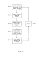
- step S100 the master-slave configuring module 690 of the current share controller establishes a master-slave relationship between voltage converting modules 200 and 300.
- the process steps performed by the master-slave configuring module 690 are shown in Fig. 7 .
- step S101 of Fig. 7 the master-slave configuring module 690 generates a master-designating control signal instructing the module to which it is addressed to function as the master in a master-slave current sharing arrangement.
- voltage converting module 200 is designated the master voltage converter.
- the signal is transmitted to module 200 by the communication module 680 of the current share controller 670, using the PMBus protocol.
- step S102 the master-slave configuring module 690 generates a slave-designating control signal instructing the module to which is addressed, namely module 300, to function as a slave in a master-slave current sharing arrangement.
- the signal is transmitted to module 300 also by the communication module 680 of the current share controller 670, using the PMBus protocol.
- the master-slave configuring module 690 need only generate and send a master-designating control signal to one of the voltage converting modules, which is to be designated as the master.
- step S102 may be omitted in this alternative embodiment.
- the module can be configured in accordance with Table loverleaf.
- both of the modules are configured to operate at a switching frequency of 140 kHz (although a frequency of 125 kHz or 150 kHz can also be used), and that the master module 200 is configured to start up before the slave module 300.
- Slave module 300 will then start up against a biased output, and its duty cycle will preferably be calculated to correspond to the bias voltage. This is done to avoid sinking current from the biased output of the master module 200.
- This pre-bias start-up method is described in international patent application WO2007/061369 A1 , the entire contents of which are incorporated herein by cross-reference.
- step S110 the power saving module 695 of the current share controller 670 communicates with the voltage converting module 200 using the communication module 680 to obtain a value indicative of the master module's output current.
- the communication module 680 communicates with the master and slave voltage converting modules using the PMBus protocol.
- the power saving module determines whether the output current is less than a threshold value. If it is not, the process proceeds to step S120, where the power saving module determines whether the slave module is switched OFF.
- step S130 the current share controller 670 executes a time delay during which the master and slave voltage converting modules operate in the current-sharing arrangement in accordance with one or more iterations of the process shown in Fig. 8 , which will be described in detail below.
- Steps S110 to S130 are then repeated unless and until it is established in step S110 that the master module's output current has fallen below the threshold value as a result of the power converter system's load current decreasing to a sufficiently low level.
- the process proceeds to step S140, where the power saving module determines, using the communication module 680, whether the slave voltage converting module 300 has been switched OFF. If it has not, the slave voltage converting module is switched OFF in step S150 by control signals which are generated by the power saving module and transmitted by the communication module, thereby reducing the system power loss that results from the running of the second (slave) voltage converting module, which is not required in a low-load situation.
- the power saving module can switch OFF the slave voltage converting module (or, more generally, one or more slave modules in the power system). This will save energy since the power loss will be lower if only one voltage converting module is running instead of two.
- step S130 proceeds to step S110. If the master voltage converting module's output current is still found to be below the threshold value, the process proceeds to step S140 and thereafter to step S130. Steps S110, S140 and S130 are therefore repeated unless and until it is determined in step S110 that the master module's output current is not less than the threshold value, whereupon the process proceeds to step S120. Since it will then be determined in step S120 that the slave module 300 has been switched OFF, the process proceeds to step S160, where the slave module is switched ON by the power saving module, in accordance with control signals send over communications bus 700 using the communication module. Voltage converting module 300 then starts up as described above and functions as a slave in accordance with its default settings. Steps 110 to S130 are thereafter repeated unless and until the master's output current is determined by the power saving module to have fallen below the threshold.
- step S200 the master voltage converting module 200 determines its output current by the current meter 210 measuring one or more sample values of the output current, and the processor 220 calculating a mean value where two or more samples have been taken.
- step S210 the master voltage converting module generates a PWM signal on the basis of the determined output current value, where a pulse width of a pulse in the signal is indicative of the master's output current level.
- the PWM signal is then filtered by an R-C filter net to give a DC current share (CS) signal whose magnitude provides a measure of the master module's output current.
- the CS signal is then transmitted to the slave voltage converting module 300 via signalling line 400.
- the master voltage converting module 200 preferably generates and sends via the signalling line 500 a synchronization (SYNC) signal to the slave voltage converting module 300.
- the SYNC signal preferably takes the form of a series of pulses whose frequency corresponds to the switching frequency of the master module or a fraction thereof.
- slave voltage converting module 300 adjusts its output current level on the basis of the CS signal received from master module 200.
- the processor 320 calculates the difference between the master's current level, as indicated by the size of the received CS signal, and the level of the slave's output current as determined by the slave's current meter 310.
- the slave module then adjusts the adjustable reference to its error amplifier 330 in dependence on the calculated difference, and thereby its switching duty cycle and output current.
- step S240 the processor 320 adjusts the phase of its switching cycle relative to the phase of the received SYNC signal, in order to reduce the input and output current ripple of the converter system 100.
- step S250 the master voltage converting module executes a time delay before again determining its output current in step S200. Steps S200 to S250 are thus repeated such that the master module 200 monitors its output current and sends signals indicative of its output current to slave module 300, which in turn adjusts its output current on the basis of the received signals. The slave module thus adjusts its output current to be substantially equal to the master module's output current.
- the power saving module 695 can, upon detecting a low-load situation, interrupt the process of Fig. 8 by turning the slave voltage converting module OFF.
- the master voltage converting module 200 may send the synchronization (SYNC) signal before or at the same time as the current share (CS) signal to the slave voltage converting module 300, i.e. step S220 may alternatively be performed before or at the same time as step S210.
- step S240 may alternatively be performed before or at the same time as step S230 by the slave module 300.
- the frequency at which steps S210 and S230 are performed is different to the frequency at which steps S220 and S240 are performed.
- the current share controller 670 may be provided as a stand-alone hardware component, or may be integrated as part of an on-board system controller 600, as shown, or integrated into one of the voltage converting modules. Alternatively, the current share controller may be provided as part of an off-board controller.
- the current share signal transmitted from the master voltage converting module 200 to the slave voltage converting module 300 takes the form of a DC signal whose voltage level is indicative of the master module's output current
- other signals can be used.
- the master module 200 dispenses with the aforementioned R-C filter net and is arranged to transmit a PWM signal generated on the basis of its output current to the slave module.
- the slave module is configured to measure the pulse width or duty cycle of the received PWM signal and to adjust its output current on the basis of the measured value. Signals of this form have the advantage of making the CS communications less susceptible to noise and interference on the CS signalling line 400, since these have little effect on the PWM pulse width.
- the slave voltage converting module is preferably configured to generate a timing signal by detecting leading and/or trailing edge pulses of the PWM signal, and to adjust the phase of its switching cycle relative to the timing signal so as to reduce the input and output ripple current of the voltage converter system 100.
- both the CS and SYNC signals are conveyed by means of the PWM signal along only one signalling line.
- the frequency of the PWM signal is preferably the same as the switching frequency of the master voltage converting module.
Landscapes
- Engineering & Computer Science (AREA)
- Power Engineering (AREA)
- Dc-Dc Converters (AREA)
- Inverter Devices (AREA)
Claims (10)
- Stromumrichtersystem (100), Folgendes umfassend:ein erstes Spannungsumwandlungsmodul (200), um eine Eingangsspannung in eine Ausgangsspannung umzuwandeln;ein zweites Spannungsumwandlungsmodul (300), um die Eingangsspannung in eine Ausgangsspannung umzuwandeln, wobei das zweite Spannungsumwandlungsmodul parallel an das erste Spannungsumwandlungsmodul angeschlossen ist, worin die ersten und zweiten Spannungsumwandlungsmodule dazu angeordnet sind, in einer Stromteilungskonfiguration zu arbeiten, um einen Laststrom des Stromumrichtersystems (100) zu teilen; undmindestens eine Signalisierungsleitung (400) zwischen dem ersten Spannungsumwandlungsmodul (200) und dem zweiten Spannungsumwandlungsmodul (300),dadurch gekennzeichnet, dass es außerdem umfasst:einen Stromteilungscontroller (600), betriebsfähig angeschlossen, um mit den ersten und zweiten Spannungsumwandlungsmodulen (200, 300) unter Verwendung des PMBus(Power Management Bus)-Protokolls zu kommunizieren, um ein Master-Slave-Verhältnis zwischen den ersten und zweiten Spannungsumwandlungsmodulen aufzubauen, ein Master-Spannungsumwandlungsmodul (200) und ein Slave-Spannungsumwandlungsmodul (300) umfassend,worin das Master-Spannungsumwandlungsmodul (200) dazu angeordnet ist, seinen Ausgangsstrom zu bestimmen und ein für seinen Ausgangsstrom bezeichnendes Signal über die mindestens eine Signalisierungsleitung (400) an das Slave-Spannungsumwandlungsmodul (300) zu senden, und das Slave-Spannungsumwandlungsmodul (300) dazu angeordnet ist, seinen Ausgangsstrom in Abhängigkeit vom Signal von dem Master-Spannungsumwandlungsmodul (200) anzupassen.
- Stromumrichtersystem nach Anspruch 1, worin der Stromteilungscontroller (600) dazu angeordnet ist, das PMBus-Protokoll zu verwenden, um den Ausgangsstrom des Master-Spannungsumwandlungsmoduls (200) zu überwachen und dem Slave-Spannungsumwandlungsmodul (300) ein Signal zu senden, das das Slave-Spannungsumwandlungsmodul anweist, auszuschalten, wenn während des Betriebs des Stromumrichtersystems (100) die Stromabgabe durch das Master-Spannungsumwandlungsmodul unter einen Schwellenwert fällt.
- Stromumrichtersystem nach Anspruch 1 oder Anspruch 2, worin:das Master-Spannungsumwandlungsmodul (200) dazu angeordnet ist, ein Signal mit modulierter Pulsbreite über die mindestens eine Signalisierungsleitung (400) an das Slave-Spannungsumwandlungsmodul (300) zu senden, wobei eine Pulsbreite des Signals mit modulierter Pulsbreite für den Ausgangsstrom des Master-Spannungsumwandlungsmoduls bezeichnend ist; unddas Slave-Spannungsumwandlungsmodul (300) dazu angeordnet ist, die Pulsbreite des Signals mit modulierter Pulsbreite zu messen und seinen Ausgangsstrom in Abhängigkeit von der gemessenen Pulsbreite anzupassen.
- Stromumrichtersystem nach Anspruch 3, worin:sowohl das erste Spannungsumwandlungsmodul (200) als auch das zweite Spannungsumwandlungsmodul (300) eine Schaltmodus-Stromversorgung ist, wobei die ersten und zweiten Spannungsumwandlungsmodule dazu angeordnet sind, in Betrieb mit jeweiligen Schaltfrequenzen zu arbeiten, die im Wesentlichen gleich sind; unddas Slave-Spannungsumwandlungsmodul (300) dazu angeordnet ist, ein Timing-Signal zu erzeugen, indem es Flanken des Signals mit modulierter Pulsbreite erkennt, und eine Phase eines Schaltzyklus des Slave-Spannungsumwandlungsmoduls (300) relativ zum Timing-Signal anzupassen, um eine Stromwelligkeit des Stromumrichtersystems (100) zu reduzieren.
- Stromumrichtersystem nach Anspruch 1 oder Anspruch 2, worin:sowohl das erste Spannungsumwandlungsmodul (200) als auch das zweite Spannungsumwandlungsmodul (300) eine Schaltmodus-Stromversorgung ist, wobei die ersten und zweiten Spannungsumwandlungsmodule dazu angeordnet sind, in Betrieb mit jeweiligen Schaltfrequenzen zu arbeiten, die im Wesentlichen gleich sind;wobei das Master-Spannungsumwandlungsmodul (200) angeordnet ist zum:Senden des für seinen Ausgangsstrom bezeichnenden Signals an das Slave-Spannungsumwandlungsmodul (300), indem eine Spannung an eine erste Signalisierungsleitung (400) angelegt wird, wobei die Größe der Spannung für den Ausgangsstrom des Master-Spannungsumwandlungsmoduls bezeichnend ist; undSenden eines Synchronisationssignals an das Slave-Spannungsumwandlungsmodul (300) über eine zweite Signalisierungsleitung (500); unddas Slave-Spannungsumwandlungsmodul (300) angeordnet ist zum:Messen der Größe der an die erste Signalisierungsleitung (400) durch das Master-Spannungsumwandlungsmodul (200) angelegten Spannung und Anpassen seines Ausgangsstroms in Abhängigkeit von der gemessenen Spannungsgröße; undAnpassen einer Phase eines Schaltzyklus des Slave-Spannungsumwandlungsmoduls (300) relativ zum Synchronisationssignal, um eine Stromwelligkeit des Stromumrichtersystems (100) zu reduzieren.
- In einem Stromumrichtersystem (100), Folgendes umfassend:ein erstes Spannungsumwandlungsmodul (200), um eine Eingangsspannung in eine Ausgangsspannung umzuwandeln;ein zweites Spannungsumwandlungsmodul (300), um die Eingangsspannung in eine Ausgangsspannung umzuwandeln, wobei das zweite Spannungsumwandlungsmodul parallel an das erste Spannungsumwandlungsmodul angeschlossen ist;einen Stromteilungscontroller (670), betriebsfähig angeschlossen, um mit den ersten und zweiten Spannungsumwandlungsmodulen (200, 300) unter Verwendung des PMBus(Power Management Bus)-Protokolls zu kommunizieren; undmindestens eine Signalisierungsleitung (400) zwischen dem ersten Spannungsumwandlungsmodul (200) und dem zweiten Spannungsumwandlungsmodul (300);ein Verfahren zum Betreiben der ersten und zweiten Spannungsumwandlungsmodule (200, 300) in einer Stromteilungskonfiguration, um einen Laststrom des Stromumrichtersystems (100) zu teilen, Folgendes umfassend:den Stromteilungscontroller, der mit mindestens einem der ersten und zweiten Spannungsumwandlungsmodule (200, 300) unter Verwendung des PMBus(Power Management Bus)-Protokolls kommuniziert, um ein Master-Slave-Verhältnis zwischen den ersten und zweiten Spannungsumwandlungsmodulen aufzubauen (S100), ein Master-Spannungsumwandlungsmodul (200) und ein Slave-Spannungsumwandlungsmodul (300) umfassend;das Master-Spannungsumwandlungsmodul (200), das dadurch eine Stromabgabe bestimmt (S200);wobei das Master-Spannungsumwandlungsmodul (200) ein für seinen Ausgangsstrom bezeichnendes Signal über die mindestens eine Signalisierungsleitung an das Slave-Spannungsumwandlungsmodul (300) sendet (S210); unddas Slave-Spannungsumwandlungsmodul seinen Ausgangsstrom in Abhängigkeit vom Signal von dem Master-Spannungsumwandlungsmodul (200) anpasst (S230).
- Verfahren nach Anspruch 6, außerdem umfassend, dass der Stromteilungscontroller (670) das PMBus-Protokoll verwendet, um den Ausgangsstrom des Master-Spannungsumwandlungsmoduls (200) zu überwachen (S 110) und dem Slave-Spannungsumwandlungsmodul (300) ein Signal zu senden (S150), das das Slave-Spannungsumwandlungsmodul anweist, auszuschalten, wenn die Stromabgabe durch das Master-Spannungsumwandlungsmodul (200) unter einen Schwellenwert fällt.
- Verfahren nach Anspruch 6 oder Anspruch 7, worin:das Master-Spannungsumwandlungsmodul (200) ein für seinen Ausgangsstrom bezeichnendes Signal an das Slave-Spannungsumwandlungsmodul (300) sendet (S210), das ein Signal mit modulierter Pulsbreite umfasst, in dem eine Pulsbreite eines Pulses für den Ausgangsstrom des Master-Spannungsumwandlungsmoduls (200) bezeichnend ist; unddas Slave-Spannungsumwandlungsmodul (300) seinen Ausgangsstrom anpasst (S230), indem es die Pulsbreite des Signals mit modulierter Pulsbreite misst und seinen Ausgangsstrom in Abhängigkeit von der gemessenen Pulsbreite anpasst.
- Verfahren nach Anspruch 8, worin sowohl das erste Spannungsumwandlungsmodul (200) als auch das zweite Spannungsumwandlungsmodul (300) eine Schaltmodus-Stromversorgung ist, wobei die ersten und zweiten Spannungsumwandlungsmodule dazu angeordnet sind, mit jeweiligen Schaltfrequenzen zu arbeiten, die im Wesentlichen gleich sind;
und worin das Verfahren außerdem umfasst:Erzeugen (240) eines Timing-Signals im Slave-Spannungsumwandlungsmodul, indem Flanken des Signals mit modulierter Pulsbreite erkannt werden; undAnpassen (240) einer Phase eines Schaltzyklus des Slave-Spannungsumwandlungsmoduls relativ zum Timing-Signal, um eine Stromwelligkeit des Stromumrichtersystems zu reduzieren. - Verfahren nach Anspruch 6 oder Anspruch 7, worin sowohl das erste Spannungsumwandlungsmodul (200) als auch das zweite Spannungsumwandlungsmodul (300) eine Schaltmodus-Stromversorgung ist, wobei die ersten und zweiten Spannungsumwandlungsmodule dazu angeordnet sind, mit jeweiligen Schaltfrequenzen zu arbeiten, die im Wesentlichen gleich sind, und worin:das Master-Spannungsumwandlungsmodul (200) ein für seinen Ausgangsstrom bezeichnendes Signal an das Slave-Spannungsumwandlungsmodul (300) sendet (S210), indem es eine Spannung an eine erste Signalisierungsleitung (400) anlegt, wobei die Größe der Spannung für den Ausgangsstrom des Master-Spannungsumwandlungsmoduls (200) bezeichnend ist;das Verfahren außerdem umfasst, dass das Master-Spannungsumwandlungsmodul (200) ein Synchronisationssignal an das Slave-Spannungsumwandlungsmodul (300) über eine zweite Signalisierungsleitung (500) sendet (S220);das Slave-Spannungsumwandlungsmodul (300) seinen Ausgangsstrom anpasst (S230), indem es die Größe der durch das Master-Spannungsumwandlungsmodul (200) an die erste Signalisierungsleitung (400) angelegten Spannung misst und seinen Ausgangsstrom in Abhängigkeit von der gemessenen Spannungsgröße anpasst; unddas Verfahren außerdem umfasst, dass das Slave-Spannungsumwandlungsmodul (300) eine Phase seines Schaltzyklus relativ zum Synchronisationssignal anpasst (S240), um eine Stromwelligkeit des Stromumrichtersystems (100) zu reduzieren.
Applications Claiming Priority (2)
| Application Number | Priority Date | Filing Date | Title |
|---|---|---|---|
| US16581409P | 2009-04-01 | 2009-04-01 | |
| PCT/EP2009/067635 WO2010112094A1 (en) | 2009-04-01 | 2009-12-21 | Current share configuration in a power converter system |
Publications (2)
| Publication Number | Publication Date |
|---|---|
| EP2415148A1 EP2415148A1 (de) | 2012-02-08 |
| EP2415148B1 true EP2415148B1 (de) | 2014-08-13 |
Family
ID=41725526
Family Applications (1)
| Application Number | Title | Priority Date | Filing Date |
|---|---|---|---|
| EP09804191.6A Not-in-force EP2415148B1 (de) | 2009-04-01 | 2009-12-21 | Lastteilungskonfiguration in einem stromumrichtersystem |
Country Status (4)
| Country | Link |
|---|---|
| US (1) | US8810217B2 (de) |
| EP (1) | EP2415148B1 (de) |
| CN (1) | CN102365812B (de) |
| WO (1) | WO2010112094A1 (de) |
Cited By (1)
| Publication number | Priority date | Publication date | Assignee | Title |
|---|---|---|---|---|
| EP4651358A1 (de) * | 2024-05-14 | 2025-11-19 | Denso Wave Incorporated | Leistungsumwandlungsvorrichtung, stromversorgungssystem und leistungsumwandlungsschaltung |
Families Citing this family (34)
| Publication number | Priority date | Publication date | Assignee | Title |
|---|---|---|---|---|
| US9013073B2 (en) * | 2010-04-22 | 2015-04-21 | Hewlett-Packard Development Company, L.P. | System and method for balancing input current with parallel power supplies |
| US10036768B2 (en) * | 2011-08-29 | 2018-07-31 | Landis+Gyr Llc | Method and arrangement for controlling DC power output in utility meter |
| JP5387651B2 (ja) * | 2011-10-21 | 2014-01-15 | 株式会社デンソー | 電源システム |
| US9077244B2 (en) | 2012-05-30 | 2015-07-07 | Linear Technology Corporation | Expanding DC/DC converter into multiphase DC/DC converter |
| EP2752983B1 (de) * | 2012-06-18 | 2015-12-09 | Mitsubishi Electric Corporation | Umrichtersystem und kommunikationsverfahren |
| WO2015020317A1 (ko) * | 2013-08-05 | 2015-02-12 | 주식회사 루비 | 전력소자 구동모듈, 그리고 이를 이용한 전력 변환 시스템 |
| CN104730976A (zh) * | 2013-12-24 | 2015-06-24 | 理察·蓝德立·葛瑞 | 于同一直流总线控制多个电器的控制方法 |
| US10447074B2 (en) | 2014-02-27 | 2019-10-15 | Hewlett Packard Enterprise Development Lp | Behavior modification of a power supply in response to a detected condition |
| US9853689B2 (en) * | 2014-11-07 | 2017-12-26 | VoltServer, Inc. | Packet energy transfer power control elements |
| CN105990999A (zh) * | 2015-01-27 | 2016-10-05 | 台达电子工业股份有限公司 | 电源供应装置及其控制方法 |
| CN104767385B (zh) * | 2015-04-13 | 2017-03-01 | 湖北三江航天万峰科技发展有限公司 | 一种基于PMBus总线的数字电源 |
| US10396582B2 (en) * | 2015-07-01 | 2019-08-27 | Maxim Integrated Products, Inc. | Master slave charging architecture with communication between chargers |
| JP6489700B2 (ja) * | 2016-01-14 | 2019-03-27 | コーセル株式会社 | 電源装置 |
| TWI592958B (zh) * | 2016-03-31 | 2017-07-21 | 全漢企業股份有限公司 | 磁性元件的製造方法 |
| US9748830B1 (en) * | 2016-09-30 | 2017-08-29 | Astec International Limited | Control circuits using different master-slave current sharing modes |
| US9960676B1 (en) * | 2016-11-01 | 2018-05-01 | Excelitas Technologies Corp. | Load sharing between parallel connected power converters |
| CN106655220A (zh) * | 2016-11-14 | 2017-05-10 | 郑州云海信息技术有限公司 | 一种改善最大均流法低频振荡的方法 |
| CN108258591A (zh) * | 2016-12-28 | 2018-07-06 | 航天信息股份有限公司 | 电源箱 |
| US10116231B2 (en) * | 2017-03-16 | 2018-10-30 | Dell Products, L.P. | Digital current-sharing loop design of PSUs to ensure output voltage regulation during dynamic load transients |
| GB2560958B (en) * | 2017-03-30 | 2022-08-31 | Bowman Power Group Ltd | Power electronics system comprising parallel inverters |
| CN108108318B (zh) * | 2018-01-25 | 2024-03-26 | 南昌市科陆智能电网科技有限公司 | 一种ttl转mbus通讯终端 |
| US11536754B2 (en) | 2019-08-15 | 2022-12-27 | Landis+Gyr Innovations, Inc. | Electricity meter with fault tolerant power supply |
| JP7436812B2 (ja) * | 2020-03-02 | 2024-02-22 | シンフォニアテクノロジー株式会社 | インバータ試験装置 |
| CN113364114A (zh) * | 2020-03-04 | 2021-09-07 | 台达电子工业股份有限公司 | 智慧电网系统及其功率管理方法 |
| KR20220037280A (ko) * | 2020-09-17 | 2022-03-24 | 삼성전자주식회사 | 전력 제공 방법 및 이를 이용하는 전자 장치 |
| JP7634975B2 (ja) * | 2020-11-30 | 2025-02-25 | 株式会社アドバンテスト | 電源装置、電源ユニット、試験装置 |
| JP7485095B2 (ja) * | 2021-01-19 | 2024-05-16 | 株式会社村田製作所 | 電源システム装置 |
| CA3158873A1 (en) * | 2021-05-14 | 2022-11-14 | Queen's University At Kingston | Methods and circuits for sensing isolated power converter output voltage across the isolation barrier |
| US12040641B2 (en) | 2021-06-22 | 2024-07-16 | Appleton Grp Llc | Systems and methods for situational suppression of overcurrent protection |
| US11994962B2 (en) * | 2021-11-04 | 2024-05-28 | Rockwell Automation Technologies, Inc. | Concurrent operation of input/output (IO) modules in a duplex configuration |
| CN114513110A (zh) * | 2022-01-20 | 2022-05-17 | 华为数字能源技术有限公司 | 一种母板、功率变换方法及装置 |
| CN114614672B (zh) * | 2022-03-14 | 2025-10-31 | 长沙广义变流技术有限公司 | 一种高频辅助变流器及其控制方法 |
| KR102816828B1 (ko) * | 2024-09-26 | 2025-06-05 | 민맥스 주식회사 | 컨버터 고장 진단 방법 및 고장 진단 기능을 갖는 컨버터 시스템 |
| CN120385912B (zh) * | 2025-06-27 | 2025-09-12 | 北京迪赛奇正科技有限公司 | 一种无源均流电路故障诊断方法、系统及程序产品 |
Family Cites Families (9)
| Publication number | Priority date | Publication date | Assignee | Title |
|---|---|---|---|---|
| US5157269A (en) * | 1991-01-31 | 1992-10-20 | Unitrode Corporation | Load current sharing circuit |
| US5847950A (en) | 1997-02-19 | 1998-12-08 | Electronic Measurements, Inc. | Control system for a power supply |
| US6236582B1 (en) * | 2000-02-01 | 2001-05-22 | Micro Linear Corporation | Load share controller for balancing current between multiple supply modules |
| US7249267B2 (en) * | 2002-12-21 | 2007-07-24 | Power-One, Inc. | Method and system for communicating filter compensation coefficients for a digital power control system |
| US6788036B1 (en) * | 2003-03-28 | 2004-09-07 | Ower-One Limited | Method and system for current sharing among a plurality of power modules |
| CN101313263B (zh) | 2005-11-23 | 2010-11-03 | 艾利森电话股份有限公司 | 同步整流电源变换器用的预偏置电路 |
| US7888918B2 (en) * | 2006-08-10 | 2011-02-15 | International Rectifier Corporation | Control circuit for multi-phase converter |
| US7629823B2 (en) * | 2006-10-04 | 2009-12-08 | Power Integrations, Inc. | Method and apparatus for pulse width modulation |
| US7772821B2 (en) | 2007-06-12 | 2010-08-10 | Analog Devices, Inc. | Digital current share bus interface |
-
2009
- 2009-12-21 EP EP09804191.6A patent/EP2415148B1/de not_active Not-in-force
- 2009-12-21 US US13/262,488 patent/US8810217B2/en active Active
- 2009-12-21 CN CN200980158604.6A patent/CN102365812B/zh not_active Expired - Fee Related
- 2009-12-21 WO PCT/EP2009/067635 patent/WO2010112094A1/en not_active Ceased
Cited By (1)
| Publication number | Priority date | Publication date | Assignee | Title |
|---|---|---|---|---|
| EP4651358A1 (de) * | 2024-05-14 | 2025-11-19 | Denso Wave Incorporated | Leistungsumwandlungsvorrichtung, stromversorgungssystem und leistungsumwandlungsschaltung |
Also Published As
| Publication number | Publication date |
|---|---|
| US20120169311A1 (en) | 2012-07-05 |
| US8810217B2 (en) | 2014-08-19 |
| EP2415148A1 (de) | 2012-02-08 |
| CN102365812B (zh) | 2015-11-25 |
| WO2010112094A1 (en) | 2010-10-07 |
| CN102365812A (zh) | 2012-02-29 |
Similar Documents
| Publication | Publication Date | Title |
|---|---|---|
| EP2415148B1 (de) | Lastteilungskonfiguration in einem stromumrichtersystem | |
| US10812664B2 (en) | Power transmission system for wireless communication systems | |
| EP3051663B1 (de) | Drahtlose stromversorgung und stromübertragungsvorrichtung | |
| US7007176B2 (en) | System and method for highly phased power regulation using adaptive compensation control | |
| US6795009B2 (en) | System and method for current handling in a digitally-controlled power converter | |
| US6563294B2 (en) | System and method for highly phased power regulation | |
| US20040075600A1 (en) | Data processor controlled DC to DC converter system and method of operation | |
| EP1618442B1 (de) | Verfahren und system zum strom-sharing zwischen mehreren leistungsmodulen | |
| EP3832870B1 (de) | Mehrphasige gleichstromwandler mit phasenabschaltung und untereinheiten und verfahren dafür | |
| EP1325547A2 (de) | Verfahren und vorrichtung zur hochphasenleistungsregelung | |
| KR20180008619A (ko) | 어댑터 및 충전 제어 방법 | |
| US11381091B2 (en) | Processing circuit with multiple power supply ports and electronic device | |
| WO2005053143A1 (en) | Power converter having improved control | |
| TW201318374A (zh) | 在乙太網路上供電之系統中之電力結合 | |
| US10418826B2 (en) | Battery device and charging device | |
| CN116114131A (zh) | 电源系统和电源单元 | |
| RU2613179C2 (ru) | Способ подачи питания и источник питания с USB-интерфейсом для нагрузочной системы множественного доступа с временным разделением каналов | |
| CN109510486B (zh) | 控制电路、芯片、系统及方法 | |
| JP6593927B2 (ja) | スイッチング電源装置 | |
| EP3278439B1 (de) | Constant-on-time (cot)-steuerung in einem isolierten wandler | |
| CN114567178B (zh) | 一种基于电流互感器的dc/dc变换器多模块并联均流线路 | |
| US12360167B2 (en) | Energy storage system and method of control | |
| JP2001057779A (ja) | スイッチング電源装置 | |
| CN110165903B (zh) | 一种双向dc/dc变换器换向控制方法及系统 | |
| JP2004294024A (ja) | 給湯システム |
Legal Events
| Date | Code | Title | Description |
|---|---|---|---|
| PUAI | Public reference made under article 153(3) epc to a published international application that has entered the european phase |
Free format text: ORIGINAL CODE: 0009012 |
|
| 17P | Request for examination filed |
Effective date: 20110902 |
|
| AK | Designated contracting states |
Kind code of ref document: A1 Designated state(s): AT BE BG CH CY CZ DE DK EE ES FI FR GB GR HR HU IE IS IT LI LT LU LV MC MK MT NL NO PL PT RO SE SI SK SM TR |
|
| DAX | Request for extension of the european patent (deleted) | ||
| 17Q | First examination report despatched |
Effective date: 20130311 |
|
| GRAP | Despatch of communication of intention to grant a patent |
Free format text: ORIGINAL CODE: EPIDOSNIGR1 |
|
| INTG | Intention to grant announced |
Effective date: 20140410 |
|
| GRAS | Grant fee paid |
Free format text: ORIGINAL CODE: EPIDOSNIGR3 |
|
| GRAA | (expected) grant |
Free format text: ORIGINAL CODE: 0009210 |
|
| AK | Designated contracting states |
Kind code of ref document: B1 Designated state(s): AT BE BG CH CY CZ DE DK EE ES FI FR GB GR HR HU IE IS IT LI LT LU LV MC MK MT NL NO PL PT RO SE SI SK SM TR |
|
| REG | Reference to a national code |
Ref country code: GB Ref legal event code: FG4D |
|
| REG | Reference to a national code |
Ref country code: CH Ref legal event code: EP Ref country code: AT Ref legal event code: REF Ref document number: 682722 Country of ref document: AT Kind code of ref document: T Effective date: 20140815 |
|
| REG | Reference to a national code |
Ref country code: IE Ref legal event code: FG4D |
|
| REG | Reference to a national code |
Ref country code: DE Ref legal event code: R096 Ref document number: 602009026028 Country of ref document: DE Effective date: 20140925 |
|
| REG | Reference to a national code |
Ref country code: NL Ref legal event code: VDEP Effective date: 20140813 |
|
| REG | Reference to a national code |
Ref country code: AT Ref legal event code: MK05 Ref document number: 682722 Country of ref document: AT Kind code of ref document: T Effective date: 20140813 |
|
| REG | Reference to a national code |
Ref country code: LT Ref legal event code: MG4D |
|
| PG25 | Lapsed in a contracting state [announced via postgrant information from national office to epo] |
Ref country code: GR Free format text: LAPSE BECAUSE OF FAILURE TO SUBMIT A TRANSLATION OF THE DESCRIPTION OR TO PAY THE FEE WITHIN THE PRESCRIBED TIME-LIMIT Effective date: 20141114 Ref country code: PT Free format text: LAPSE BECAUSE OF FAILURE TO SUBMIT A TRANSLATION OF THE DESCRIPTION OR TO PAY THE FEE WITHIN THE PRESCRIBED TIME-LIMIT Effective date: 20141215 Ref country code: FI Free format text: LAPSE BECAUSE OF FAILURE TO SUBMIT A TRANSLATION OF THE DESCRIPTION OR TO PAY THE FEE WITHIN THE PRESCRIBED TIME-LIMIT Effective date: 20140813 Ref country code: SE Free format text: LAPSE BECAUSE OF FAILURE TO SUBMIT A TRANSLATION OF THE DESCRIPTION OR TO PAY THE FEE WITHIN THE PRESCRIBED TIME-LIMIT Effective date: 20140813 Ref country code: ES Free format text: LAPSE BECAUSE OF FAILURE TO SUBMIT A TRANSLATION OF THE DESCRIPTION OR TO PAY THE FEE WITHIN THE PRESCRIBED TIME-LIMIT Effective date: 20140813 Ref country code: LT Free format text: LAPSE BECAUSE OF FAILURE TO SUBMIT A TRANSLATION OF THE DESCRIPTION OR TO PAY THE FEE WITHIN THE PRESCRIBED TIME-LIMIT Effective date: 20140813 Ref country code: BG Free format text: LAPSE BECAUSE OF FAILURE TO SUBMIT A TRANSLATION OF THE DESCRIPTION OR TO PAY THE FEE WITHIN THE PRESCRIBED TIME-LIMIT Effective date: 20141113 Ref country code: NO Free format text: LAPSE BECAUSE OF FAILURE TO SUBMIT A TRANSLATION OF THE DESCRIPTION OR TO PAY THE FEE WITHIN THE PRESCRIBED TIME-LIMIT Effective date: 20141113 |
|
| PG25 | Lapsed in a contracting state [announced via postgrant information from national office to epo] |
Ref country code: HR Free format text: LAPSE BECAUSE OF FAILURE TO SUBMIT A TRANSLATION OF THE DESCRIPTION OR TO PAY THE FEE WITHIN THE PRESCRIBED TIME-LIMIT Effective date: 20140813 Ref country code: CY Free format text: LAPSE BECAUSE OF FAILURE TO SUBMIT A TRANSLATION OF THE DESCRIPTION OR TO PAY THE FEE WITHIN THE PRESCRIBED TIME-LIMIT Effective date: 20140813 Ref country code: AT Free format text: LAPSE BECAUSE OF FAILURE TO SUBMIT A TRANSLATION OF THE DESCRIPTION OR TO PAY THE FEE WITHIN THE PRESCRIBED TIME-LIMIT Effective date: 20140813 Ref country code: LV Free format text: LAPSE BECAUSE OF FAILURE TO SUBMIT A TRANSLATION OF THE DESCRIPTION OR TO PAY THE FEE WITHIN THE PRESCRIBED TIME-LIMIT Effective date: 20140813 Ref country code: IS Free format text: LAPSE BECAUSE OF FAILURE TO SUBMIT A TRANSLATION OF THE DESCRIPTION OR TO PAY THE FEE WITHIN THE PRESCRIBED TIME-LIMIT Effective date: 20141213 |
|
| PG25 | Lapsed in a contracting state [announced via postgrant information from national office to epo] |
Ref country code: NL Free format text: LAPSE BECAUSE OF FAILURE TO SUBMIT A TRANSLATION OF THE DESCRIPTION OR TO PAY THE FEE WITHIN THE PRESCRIBED TIME-LIMIT Effective date: 20140813 |
|
| PG25 | Lapsed in a contracting state [announced via postgrant information from national office to epo] |
Ref country code: EE Free format text: LAPSE BECAUSE OF FAILURE TO SUBMIT A TRANSLATION OF THE DESCRIPTION OR TO PAY THE FEE WITHIN THE PRESCRIBED TIME-LIMIT Effective date: 20140813 Ref country code: SK Free format text: LAPSE BECAUSE OF FAILURE TO SUBMIT A TRANSLATION OF THE DESCRIPTION OR TO PAY THE FEE WITHIN THE PRESCRIBED TIME-LIMIT Effective date: 20140813 Ref country code: RO Free format text: LAPSE BECAUSE OF FAILURE TO SUBMIT A TRANSLATION OF THE DESCRIPTION OR TO PAY THE FEE WITHIN THE PRESCRIBED TIME-LIMIT Effective date: 20140813 Ref country code: CZ Free format text: LAPSE BECAUSE OF FAILURE TO SUBMIT A TRANSLATION OF THE DESCRIPTION OR TO PAY THE FEE WITHIN THE PRESCRIBED TIME-LIMIT Effective date: 20140813 Ref country code: DK Free format text: LAPSE BECAUSE OF FAILURE TO SUBMIT A TRANSLATION OF THE DESCRIPTION OR TO PAY THE FEE WITHIN THE PRESCRIBED TIME-LIMIT Effective date: 20140813 |
|
| REG | Reference to a national code |
Ref country code: DE Ref legal event code: R097 Ref document number: 602009026028 Country of ref document: DE |
|
| PG25 | Lapsed in a contracting state [announced via postgrant information from national office to epo] |
Ref country code: PL Free format text: LAPSE BECAUSE OF FAILURE TO SUBMIT A TRANSLATION OF THE DESCRIPTION OR TO PAY THE FEE WITHIN THE PRESCRIBED TIME-LIMIT Effective date: 20140813 |
|
| PLBE | No opposition filed within time limit |
Free format text: ORIGINAL CODE: 0009261 |
|
| STAA | Information on the status of an ep patent application or granted ep patent |
Free format text: STATUS: NO OPPOSITION FILED WITHIN TIME LIMIT |
|
| PG25 | Lapsed in a contracting state [announced via postgrant information from national office to epo] |
Ref country code: BE Free format text: LAPSE BECAUSE OF NON-PAYMENT OF DUE FEES Effective date: 20141231 |
|
| 26N | No opposition filed |
Effective date: 20150515 |
|
| PG25 | Lapsed in a contracting state [announced via postgrant information from national office to epo] |
Ref country code: LU Free format text: LAPSE BECAUSE OF FAILURE TO SUBMIT A TRANSLATION OF THE DESCRIPTION OR TO PAY THE FEE WITHIN THE PRESCRIBED TIME-LIMIT Effective date: 20141221 |
|
| REG | Reference to a national code |
Ref country code: CH Ref legal event code: PL |
|
| REG | Reference to a national code |
Ref country code: IE Ref legal event code: MM4A |
|
| PG25 | Lapsed in a contracting state [announced via postgrant information from national office to epo] |
Ref country code: IE Free format text: LAPSE BECAUSE OF NON-PAYMENT OF DUE FEES Effective date: 20141221 Ref country code: LI Free format text: LAPSE BECAUSE OF NON-PAYMENT OF DUE FEES Effective date: 20141231 Ref country code: CH Free format text: LAPSE BECAUSE OF NON-PAYMENT OF DUE FEES Effective date: 20141231 |
|
| PG25 | Lapsed in a contracting state [announced via postgrant information from national office to epo] |
Ref country code: SI Free format text: LAPSE BECAUSE OF FAILURE TO SUBMIT A TRANSLATION OF THE DESCRIPTION OR TO PAY THE FEE WITHIN THE PRESCRIBED TIME-LIMIT Effective date: 20140813 |
|
| REG | Reference to a national code |
Ref country code: FR Ref legal event code: PLFP Year of fee payment: 7 |
|
| PG25 | Lapsed in a contracting state [announced via postgrant information from national office to epo] |
Ref country code: SM Free format text: LAPSE BECAUSE OF FAILURE TO SUBMIT A TRANSLATION OF THE DESCRIPTION OR TO PAY THE FEE WITHIN THE PRESCRIBED TIME-LIMIT Effective date: 20140813 |
|
| PG25 | Lapsed in a contracting state [announced via postgrant information from national office to epo] |
Ref country code: MC Free format text: LAPSE BECAUSE OF FAILURE TO SUBMIT A TRANSLATION OF THE DESCRIPTION OR TO PAY THE FEE WITHIN THE PRESCRIBED TIME-LIMIT Effective date: 20140813 |
|
| PG25 | Lapsed in a contracting state [announced via postgrant information from national office to epo] |
Ref country code: HU Free format text: LAPSE BECAUSE OF FAILURE TO SUBMIT A TRANSLATION OF THE DESCRIPTION OR TO PAY THE FEE WITHIN THE PRESCRIBED TIME-LIMIT; INVALID AB INITIO Effective date: 20091221 Ref country code: TR Free format text: LAPSE BECAUSE OF FAILURE TO SUBMIT A TRANSLATION OF THE DESCRIPTION OR TO PAY THE FEE WITHIN THE PRESCRIBED TIME-LIMIT Effective date: 20140813 Ref country code: MT Free format text: LAPSE BECAUSE OF FAILURE TO SUBMIT A TRANSLATION OF THE DESCRIPTION OR TO PAY THE FEE WITHIN THE PRESCRIBED TIME-LIMIT Effective date: 20140813 Ref country code: BE Free format text: LAPSE BECAUSE OF FAILURE TO SUBMIT A TRANSLATION OF THE DESCRIPTION OR TO PAY THE FEE WITHIN THE PRESCRIBED TIME-LIMIT Effective date: 20140813 |
|
| REG | Reference to a national code |
Ref country code: FR Ref legal event code: PLFP Year of fee payment: 8 |
|
| PG25 | Lapsed in a contracting state [announced via postgrant information from national office to epo] |
Ref country code: IT Free format text: LAPSE BECAUSE OF NON-PAYMENT OF DUE FEES Effective date: 20151221 |
|
| PG25 | Lapsed in a contracting state [announced via postgrant information from national office to epo] |
Ref country code: IT Free format text: LAPSE BECAUSE OF NON-PAYMENT OF DUE FEES Effective date: 20151221 |
|
| PGRI | Patent reinstated in contracting state [announced from national office to epo] |
Ref country code: IT Effective date: 20170710 |
|
| REG | Reference to a national code |
Ref country code: FR Ref legal event code: PLFP Year of fee payment: 9 |
|
| PGFP | Annual fee paid to national office [announced via postgrant information from national office to epo] |
Ref country code: FR Payment date: 20171227 Year of fee payment: 9 |
|
| PGFP | Annual fee paid to national office [announced via postgrant information from national office to epo] |
Ref country code: GB Payment date: 20171227 Year of fee payment: 9 |
|
| PGFP | Annual fee paid to national office [announced via postgrant information from national office to epo] |
Ref country code: DE Payment date: 20171229 Year of fee payment: 9 |
|
| PGFP | Annual fee paid to national office [announced via postgrant information from national office to epo] |
Ref country code: IT Payment date: 20171221 Year of fee payment: 9 |
|
| PG25 | Lapsed in a contracting state [announced via postgrant information from national office to epo] |
Ref country code: MK Free format text: LAPSE BECAUSE OF FAILURE TO SUBMIT A TRANSLATION OF THE DESCRIPTION OR TO PAY THE FEE WITHIN THE PRESCRIBED TIME-LIMIT Effective date: 20140813 |
|
| REG | Reference to a national code |
Ref country code: DE Ref legal event code: R119 Ref document number: 602009026028 Country of ref document: DE |
|
| GBPC | Gb: european patent ceased through non-payment of renewal fee |
Effective date: 20181221 |
|
| PG25 | Lapsed in a contracting state [announced via postgrant information from national office to epo] |
Ref country code: DE Free format text: LAPSE BECAUSE OF NON-PAYMENT OF DUE FEES Effective date: 20190702 Ref country code: FR Free format text: LAPSE BECAUSE OF NON-PAYMENT OF DUE FEES Effective date: 20181231 Ref country code: IT Free format text: LAPSE BECAUSE OF NON-PAYMENT OF DUE FEES Effective date: 20181221 |
|
| PG25 | Lapsed in a contracting state [announced via postgrant information from national office to epo] |
Ref country code: GB Free format text: LAPSE BECAUSE OF NON-PAYMENT OF DUE FEES Effective date: 20181221 |