EP2412021B1 - Light emitting diode - Google Patents
Light emitting diode Download PDFInfo
- Publication number
- EP2412021B1 EP2412021B1 EP10710274.1A EP10710274A EP2412021B1 EP 2412021 B1 EP2412021 B1 EP 2412021B1 EP 10710274 A EP10710274 A EP 10710274A EP 2412021 B1 EP2412021 B1 EP 2412021B1
- Authority
- EP
- European Patent Office
- Prior art keywords
- semiconductor body
- light
- emitting diode
- coupling
- diode according
- Prior art date
- Legal status (The legal status is an assumption and is not a legal conclusion. Google has not performed a legal analysis and makes no representation as to the accuracy of the status listed.)
- Active
Links
- 239000004065 semiconductor Substances 0.000 claims description 150
- 239000000463 material Substances 0.000 claims description 54
- 230000005670 electromagnetic radiation Effects 0.000 claims description 42
- 230000005855 radiation Effects 0.000 claims description 7
- 229920001296 polysiloxane Polymers 0.000 claims description 6
- GWEVSGVZZGPLCZ-UHFFFAOYSA-N Titan oxide Chemical compound O=[Ti]=O GWEVSGVZZGPLCZ-UHFFFAOYSA-N 0.000 claims description 3
- 239000000126 substance Substances 0.000 claims description 3
- PBCFLUZVCVVTBY-UHFFFAOYSA-N tantalum pentoxide Inorganic materials O=[Ta](=O)O[Ta](=O)=O PBCFLUZVCVVTBY-UHFFFAOYSA-N 0.000 claims 1
- 230000003287 optical effect Effects 0.000 description 16
- 238000010521 absorption reaction Methods 0.000 description 4
- 238000000034 method Methods 0.000 description 4
- 230000008569 process Effects 0.000 description 4
- 238000009826 distribution Methods 0.000 description 3
- 230000004888 barrier function Effects 0.000 description 2
- 239000000969 carrier Substances 0.000 description 2
- 239000002800 charge carrier Substances 0.000 description 2
- 238000006243 chemical reaction Methods 0.000 description 2
- 239000004020 conductor Substances 0.000 description 2
- 238000004519 manufacturing process Methods 0.000 description 2
- 238000005086 pumping Methods 0.000 description 2
- 229910052710 silicon Inorganic materials 0.000 description 2
- 239000010703 silicon Substances 0.000 description 2
- PFNQVRZLDWYSCW-UHFFFAOYSA-N (fluoren-9-ylideneamino) n-naphthalen-1-ylcarbamate Chemical compound C12=CC=CC=C2C2=CC=CC=C2C1=NOC(=O)NC1=CC=CC2=CC=CC=C12 PFNQVRZLDWYSCW-UHFFFAOYSA-N 0.000 description 1
- 229910052582 BN Inorganic materials 0.000 description 1
- PZNSFCLAULLKQX-UHFFFAOYSA-N Boron nitride Chemical compound N#B PZNSFCLAULLKQX-UHFFFAOYSA-N 0.000 description 1
- 239000004593 Epoxy Substances 0.000 description 1
- 229910052581 Si3N4 Inorganic materials 0.000 description 1
- VYPSYNLAJGMNEJ-UHFFFAOYSA-N Silicium dioxide Chemical compound O=[Si]=O VYPSYNLAJGMNEJ-UHFFFAOYSA-N 0.000 description 1
- 238000004026 adhesive bonding Methods 0.000 description 1
- XAGFODPZIPBFFR-UHFFFAOYSA-N aluminium Chemical compound [Al] XAGFODPZIPBFFR-UHFFFAOYSA-N 0.000 description 1
- 229910052782 aluminium Inorganic materials 0.000 description 1
- 230000008901 benefit Effects 0.000 description 1
- PMHQVHHXPFUNSP-UHFFFAOYSA-M copper(1+);methylsulfanylmethane;bromide Chemical compound Br[Cu].CSC PMHQVHHXPFUNSP-UHFFFAOYSA-M 0.000 description 1
- 230000008878 coupling Effects 0.000 description 1
- 238000010168 coupling process Methods 0.000 description 1
- 238000005859 coupling reaction Methods 0.000 description 1
- 230000007423 decrease Effects 0.000 description 1
- 238000000407 epitaxy Methods 0.000 description 1
- 238000005530 etching Methods 0.000 description 1
- 238000005304 joining Methods 0.000 description 1
- BPUBBGLMJRNUCC-UHFFFAOYSA-N oxygen(2-);tantalum(5+) Chemical compound [O-2].[O-2].[O-2].[O-2].[O-2].[Ta+5].[Ta+5] BPUBBGLMJRNUCC-UHFFFAOYSA-N 0.000 description 1
- 238000002161 passivation Methods 0.000 description 1
- 238000013139 quantization Methods 0.000 description 1
- 239000002096 quantum dot Substances 0.000 description 1
- 238000007788 roughening Methods 0.000 description 1
- HBMJWWWQQXIZIP-UHFFFAOYSA-N silicon carbide Chemical compound [Si+]#[C-] HBMJWWWQQXIZIP-UHFFFAOYSA-N 0.000 description 1
- 229910010271 silicon carbide Inorganic materials 0.000 description 1
- HQVNEWCFYHHQES-UHFFFAOYSA-N silicon nitride Chemical compound N12[Si]34N5[Si]62N3[Si]51N64 HQVNEWCFYHHQES-UHFFFAOYSA-N 0.000 description 1
- 229910052814 silicon oxide Inorganic materials 0.000 description 1
- 229910052709 silver Inorganic materials 0.000 description 1
- 239000004332 silver Substances 0.000 description 1
- 230000003595 spectral effect Effects 0.000 description 1
- 238000003892 spreading Methods 0.000 description 1
- 230000007480 spreading Effects 0.000 description 1
- 229910001936 tantalum oxide Inorganic materials 0.000 description 1
- OGIDPMRJRNCKJF-UHFFFAOYSA-N titanium oxide Inorganic materials [Ti]=O OGIDPMRJRNCKJF-UHFFFAOYSA-N 0.000 description 1
Images

Classifications
-
- H—ELECTRICITY
- H01—ELECTRIC ELEMENTS
- H01L—SEMICONDUCTOR DEVICES NOT COVERED BY CLASS H10
- H01L25/00—Assemblies consisting of a plurality of individual semiconductor or other solid state devices ; Multistep manufacturing processes thereof
- H01L25/03—Assemblies consisting of a plurality of individual semiconductor or other solid state devices ; Multistep manufacturing processes thereof all the devices being of a type provided for in the same subgroup of groups H01L27/00 - H01L33/00, or in a single subclass of H10K, H10N, e.g. assemblies of rectifier diodes
- H01L25/04—Assemblies consisting of a plurality of individual semiconductor or other solid state devices ; Multistep manufacturing processes thereof all the devices being of a type provided for in the same subgroup of groups H01L27/00 - H01L33/00, or in a single subclass of H10K, H10N, e.g. assemblies of rectifier diodes the devices not having separate containers
- H01L25/075—Assemblies consisting of a plurality of individual semiconductor or other solid state devices ; Multistep manufacturing processes thereof all the devices being of a type provided for in the same subgroup of groups H01L27/00 - H01L33/00, or in a single subclass of H10K, H10N, e.g. assemblies of rectifier diodes the devices not having separate containers the devices being of a type provided for in group H01L33/00
- H01L25/0756—Stacked arrangements of devices
-
- H—ELECTRICITY
- H01—ELECTRIC ELEMENTS
- H01L—SEMICONDUCTOR DEVICES NOT COVERED BY CLASS H10
- H01L2924/00—Indexing scheme for arrangements or methods for connecting or disconnecting semiconductor or solid-state bodies as covered by H01L24/00
- H01L2924/0001—Technical content checked by a classifier
- H01L2924/0002—Not covered by any one of groups H01L24/00, H01L24/00 and H01L2224/00
-
- H—ELECTRICITY
- H01—ELECTRIC ELEMENTS
- H01L—SEMICONDUCTOR DEVICES NOT COVERED BY CLASS H10
- H01L33/00—Semiconductor devices with at least one potential-jump barrier or surface barrier specially adapted for light emission; Processes or apparatus specially adapted for the manufacture or treatment thereof or of parts thereof; Details thereof
- H01L33/02—Semiconductor devices with at least one potential-jump barrier or surface barrier specially adapted for light emission; Processes or apparatus specially adapted for the manufacture or treatment thereof or of parts thereof; Details thereof characterised by the semiconductor bodies
- H01L33/08—Semiconductor devices with at least one potential-jump barrier or surface barrier specially adapted for light emission; Processes or apparatus specially adapted for the manufacture or treatment thereof or of parts thereof; Details thereof characterised by the semiconductor bodies with a plurality of light emitting regions, e.g. laterally discontinuous light emitting layer or photoluminescent region integrated within the semiconductor body
-
- H—ELECTRICITY
- H01—ELECTRIC ELEMENTS
- H01L—SEMICONDUCTOR DEVICES NOT COVERED BY CLASS H10
- H01L33/00—Semiconductor devices with at least one potential-jump barrier or surface barrier specially adapted for light emission; Processes or apparatus specially adapted for the manufacture or treatment thereof or of parts thereof; Details thereof
- H01L33/02—Semiconductor devices with at least one potential-jump barrier or surface barrier specially adapted for light emission; Processes or apparatus specially adapted for the manufacture or treatment thereof or of parts thereof; Details thereof characterised by the semiconductor bodies
- H01L33/20—Semiconductor devices with at least one potential-jump barrier or surface barrier specially adapted for light emission; Processes or apparatus specially adapted for the manufacture or treatment thereof or of parts thereof; Details thereof characterised by the semiconductor bodies with a particular shape, e.g. curved or truncated substrate
- H01L33/22—Roughened surfaces, e.g. at the interface between epitaxial layers
-
- H—ELECTRICITY
- H01—ELECTRIC ELEMENTS
- H01L—SEMICONDUCTOR DEVICES NOT COVERED BY CLASS H10
- H01L33/00—Semiconductor devices with at least one potential-jump barrier or surface barrier specially adapted for light emission; Processes or apparatus specially adapted for the manufacture or treatment thereof or of parts thereof; Details thereof
- H01L33/36—Semiconductor devices with at least one potential-jump barrier or surface barrier specially adapted for light emission; Processes or apparatus specially adapted for the manufacture or treatment thereof or of parts thereof; Details thereof characterised by the electrodes
- H01L33/38—Semiconductor devices with at least one potential-jump barrier or surface barrier specially adapted for light emission; Processes or apparatus specially adapted for the manufacture or treatment thereof or of parts thereof; Details thereof characterised by the electrodes with a particular shape
- H01L33/382—Semiconductor devices with at least one potential-jump barrier or surface barrier specially adapted for light emission; Processes or apparatus specially adapted for the manufacture or treatment thereof or of parts thereof; Details thereof characterised by the electrodes with a particular shape the electrode extending partially in or entirely through the semiconductor body
-
- H—ELECTRICITY
- H01—ELECTRIC ELEMENTS
- H01L—SEMICONDUCTOR DEVICES NOT COVERED BY CLASS H10
- H01L33/00—Semiconductor devices with at least one potential-jump barrier or surface barrier specially adapted for light emission; Processes or apparatus specially adapted for the manufacture or treatment thereof or of parts thereof; Details thereof
- H01L33/48—Semiconductor devices with at least one potential-jump barrier or surface barrier specially adapted for light emission; Processes or apparatus specially adapted for the manufacture or treatment thereof or of parts thereof; Details thereof characterised by the semiconductor body packages
- H01L33/50—Wavelength conversion elements
- H01L33/501—Wavelength conversion elements characterised by the materials, e.g. binder
- H01L33/502—Wavelength conversion materials
Definitions
- a light-emitting diode is specified.
- the internal efficiency in the generation of electromagnetic radiation for light-emitting diodes which are based for example on the material system InGaN, with increasing wavelength of the generated electromagnetic radiation from about 80% at a wavelength of 400 nm to about 30% at one wavelength of 540 nm decreases. That is, the internal efficiency for light emitting diodes capable of producing green light is very small compared to light emitting diodes emitting ultraviolet or blue light.
- an LED is indicated with three light-emitting layers, one being electrically pumped.
- An object to be solved is to specify a light-emitting diode with which electromagnetic radiation can be generated particularly efficiently. Another object to be solved is to provide a light-emitting diode with which, in particular, green light can be generated particularly efficiently.
- the light-emitting diode comprises a first semiconductor body.
- the semiconductor body has grown epitaxially and may be based on the InGaN material system.
- the semiconductor body comprises at least one active region, which is electrically contacted.
- electromagnetic radiation of a first wavelength range is generated in the active region of the first semiconductor body.
- the electromagnetic radiation is generated by means of an electrical operation of the active region.
- the electromagnetic radiation of the first wavelength range is, for example, electromagnetic radiation from the UV range and / or blue light.
- the light-emitting diode comprises a second semiconductor body, which is fastened to an upper side of the first semiconductor body on the first semiconductor body.
- the second semiconductor body is preferably produced epitaxially.
- the second semiconductor body may be based on the InGaN material system or the InGaAlP material system.
- the second semiconductor body comprises a re-emission region having a multiple quantum well structure.
- Quantum well structure has no significance with regard to the dimensionality of the quantization. It includes quantum wells, quantum wires and quantum dots, as well as any combination of these structures.
- electromagnetic radiation of the first wavelength range is absorbed in the re-emission range and re-emitted electromagnetic radiation of a second wavelength range.
- the second wavelength range preferably comprises electromagnetic radiation having longer wavelengths than the first wavelength range.
- the second wavelength range comprises electromagnetic radiation from the wavelength range of green and / or yellow and / or red light.
- the second semiconductor body is therefore preferably arranged such that electromagnetic radiation of the first wavelength range can enter from the first semiconductor body into the second semiconductor body.
- the second semiconductor body is preferably arranged on a radiation exit surface of the first semiconductor body.
- a majority of the electromagnetic radiation generated in the first semiconductor body enters the second Semiconductor body.
- a large part of the electromagnetic radiation is understood to be at least 50%, preferably at least 70%, particularly preferably at least 85% of the electromagnetic radiation of the first wavelength range.
- the second semiconductor body is designed to be particularly large area and preferably covers the entire radiation exit surface at the top of the first semiconductor body.
- the first and second semiconductor bodies terminate flush with one another in the lateral direction, or the second semiconductor body projects beyond the first semiconductor body in the lateral direction.
- the lateral direction is that direction which, for example, is perpendicular to an epitaxial growth direction of the first semiconductor body or which runs parallel to a layer of the first or the second semiconductor body.
- connection material is arranged between the first and the second semiconductor body, wherein the connection material mechanically connects the first and the second semiconductor body to one another.
- the connecting material may be, for example, a semiconductor material, from which the first and the second semiconductor body are formed. First and second semiconductor body are then monolithically integrated with each other.
- First and second semiconductor body are in this case, for example, produced in a single epitaxial growth process and thus integrally formed. Furthermore, it is possible for the first and second semiconductor bodies to be joined together by a wafer bonding process are connected.
- the wafer bonding process is, for example, a direct bonding or anodic bonding.
- the mutually facing surfaces of the two semiconductor bodies have no roughening and are optionally smoothed before joining.
- the bonding material is a transparent, electrically conductive material.
- the bonding material may then be a TCO (Transparent Conductive Oxide) material.
- first and second semiconductor bodies can be connected to one another, for example, by anodic or direct bonding by means of the connecting material.
- the connecting material is electrically insulating.
- the bonding material may then be, for example, a silicone, a high refractive index silicone having a refractive index greater than 1.5, an epoxy, a silicon oxide or a silicon nitride.
- First and second semiconductor bodies can then be connected together by means of the bonding material by gluing or bonding.
- the re-emission region of the second semiconductor body is preferably not electrically contacted. That is, electromagnetic radiation in the re-emission region, that is, the electromagnetic radiation of the second wavelength range, is not generated by electrically driving the multiple quantum well structure in the re-emission region but by optical driving. That is, the light-emitting diode is based inter alia on the knowledge that if the multiple quantum well structure not electrically, but optically pumped, a uniform charge distribution in the Mehrfachquantentopf Modell is possible.
- the first semiconductor body which produces short-wave electromagnetic radiation in operation with the second semiconductor body, which generates longer wavelength electromagnetic radiation during operation
- a light-emitting diode is characterized by particularly good spectral and thermal properties. That is, the active region of the first semiconductor body can be cooled particularly well, for example, because the second semiconductor body acts as a kind of heat spreader for the first semiconductor body.
- the first semiconductor body has a plurality of coupling-out structures on its upper side facing the second semiconductor body.
- the coupling-out structures may be, for example, pyramidal or truncated pyramidal elevations on the upper side of the first semiconductor body.
- the coupling-out structures are formed with a material that is different from the material of the first semiconductor body.
- the decoupling structures are additional structures.
- the coupling-out structures are preferably made of a material whose optical refractive index deviates from the refractive index of the first semiconductor body by at most 30%.
- the bonding material encloses the coupling-out structures on their exposed outer surfaces. That is, the bonding material is between the first and the second Semiconductor body introduced and covers the coupling-out.
- the connecting material can then completely cover the coupling-out structures on the exposed outer surfaces of the coupling-out structures, so that the coupling-out structures are embedded in the connecting material. It is then possible for the coupling-out structures on the upper side of the first semiconductor body not to touch the second semiconductor body, but for connecting material to be arranged between the coupling-out structures and the second semiconductor body.
- the coupling-out structures make it possible for electromagnetic radiation of the first wavelength range to emerge from the first semiconductor body with a greater probability and to enter the second semiconductor body than would be the case without the coupling-out structures.
- the coupling-out structures ensure, for example, that the probability of a total reflection of the electromagnetic radiation from the first wavelength range at the interface between the first semiconductor body and the second semiconductor body is reduced.
- the second semiconductor body has a multiplicity of coupling-out structures on its upper side facing away from the first semiconductor body and / or its underside facing the first semiconductor body.
- the coupling-out structures can be identical or different from the coupling-out structures of the first semiconductor body. That is, the coupling-out structures can be structured from the material of the second semiconductor body and thus consist of the material of the second semiconductor body. However, it is also possible that the coupling-out of a material exist, which is different from the material of the second semiconductor body.
- the second semiconductor body preferably has a multiplicity of outcoupling structures on its upper side facing away from the first semiconductor body and its underside facing the first semiconductor body.
- the coupling-out structures on the underside of the second semiconductor body advantageously reduce Fresnel losses at the interface between the second semiconductor body and connecting material.
- the coupling-out structures of the second semiconductor body consist of a material whose optical refractive index deviates from the optical refractive index of the second semiconductor body by at most 30%.
- the coupling-out structures of the second semiconductor body increase the probability of a light exit from the second semiconductor body.
- the exiting light may be electromagnetic radiation from the first or the second wavelength range. That is, the light emitting diode can emit mixed light of the first and the second wavelength range.
- the mixed light may be, for example, white light.
- the LED predominantly emits electromagnetic radiation from the second wavelength range. That is, the majority - for example, at least 90% - of the electromagnetic radiation from the first wavelength range that has entered the second semiconductor body is in the second Semiconductor body absorbed. In this way, it is possible that the light-emitting diode emits, for example, pure green, yellow or red light.
- the material of the coupling-out structures of the first and / or the second semiconductor body contains or consists of one of the following substances: titanium oxide, zinc selenide, aluminum nitride, silicon carbide, boron nitride and / or tantalum oxide. These substances are distinguished by the fact that they have an optical refractive index which deviates by at most 30% from the refractive index of an InGaN-based semiconductor body.
- a mirror layer is fastened to the underside of the first semiconductor body facing away from the second semiconductor body.
- the mirror layer is, for example, a dielectric mirror, a Bragg mirror, a metallic mirror or a combination of said mirrors.
- the mirror layer is provided to reflect electromagnetic radiation of the first wavelength range in the direction of the second semiconductor body. In this way, it is possible for a particularly large proportion of the electromagnetic radiation of the first wavelength range to enter the second semiconductor body.
- the mirror layer can also reflect electromagnetic radiation of the second wavelength range, which is emitted from the second semiconductor body in the direction of the first semiconductor body, in the direction of the second semiconductor body and thus out of the light-emitting diode.
- the multiple quantum structure of the re-emission region comprises at least 20 quantum well layers.
- the quantum well layers are arranged, for example, one above the other along a growth direction of the second semiconductor body and separated from one another by barrier layers. It has been found that such a large number of quantum well layers can be uniformly filled with carriers by optical pumping and the efficiency of generation of electromagnetic radiation of the second wavelength range is markedly increased due to the large number of quantum well layers.
- the number of quantum well layers (also quantum films) is important for the efficiency of light generation, since photons are absorbed only in the quantum well layers and a sufficient absorption cross section is given for a large number of quantum well layers , Furthermore, given a high number of quantum well layers, an advantageous shift of the maximum efficiency to higher currents results due to the lower charge carrier density in the individual pots. Therefore, full conversion at high current densities of> 100 A / cm 2 can be more efficient than a directly electrically pumped green LED.
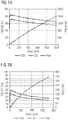
- the Figure 1A Figure 3 shows, graphically, optical loss external efficiency (EQE) and internal optical loss-free optical efficiency (IQE) for a light emitting diode emitting electromagnetic radiation at a peak wavelength of 435 nm, ie, blue light.
- the LED is electrically operated.
- the internal efficiency is up to more than 80%.
- FIG. 1B Fig. 3 shows graphically plotted external efficiency (EQE) and internal efficiency (IQE) for an electrically driven light emitting diode emitting green light at a peak wavelength of 540 nm. Like in the FIG. 1B As can be seen, the maximum internal efficiency is less than 50%.
- electrically pumped green light emitting diodes are inferior in their efficiency to electrically pumped blue light emitting diodes or UV emitting light emitting diodes.
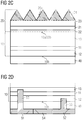
- the FIG. 2A shows a first embodiment of a light-emitting diode described here with reference to a schematic sectional view.
- the LED of the FIG. 2A comprises a first semiconductor body 10 and a second semiconductor body 20.
- First semiconductor body 10 and second semiconductor body 20 are stacked one above the other.
- the second semiconductor body 20 follows the first semiconductor body 10 on its upper side 10a.
- the upper side 10a also contains the radiation outlet surface of the first semiconductor body 10, through which all or a majority of the electromagnetic radiation 110 emerging from the first semiconductor body 10 exits.
- the first semiconductor body 10 comprises a p-doped region 12 and an n-doped region 13. Between the p-doped region 12 and the n-doped region 13, the active region 11 is arranged. The active area 11 is electrically operated, the electrical connections are in the FIG. 2A not shown (see the FIG. 2D ). By way of example, the active region 11 comprises a pn junction, a single quantum well structure or a multiple quantum well structure. On its upper side 10a, the first semiconductor body 10 has coupling-out structures 14. The coupling-out structures 14 are formed with a material that is different from the material of the first semiconductor body 10.
- the second semiconductor body 20 comprises an n-doped region 22, a p-doped region 23 and a re-emission region 21, which is arranged between the two areas.
- the re-emission region 21 comprises a multiple quantum well structure.
- the re-emission region 21 is not electrically connected and is not operated electrically.
- the second semiconductor body 20 On its upper side 20a, the second semiconductor body 20 comprises coupling-out structures 24, which in the present case are patterned into the semiconductor body 20 by means of KOH etching.
- the coupling-out structures 24 can also be formed from other materials, as described above.
- Auskoppel Genten 24 may be arranged (not shown in the figure).
- a connecting material 30 is arranged, which in the present case contains silicone or consists of silicone.
- the connecting material 30 completely encloses the coupling-out structures 14 of the first semiconductor body 10 on their exposed outer surfaces.
- the bonding material 30 is electrically insulating and represents a mechanical connection between the two semiconductor bodies.
- First semiconductor body 10 and second semiconductor body 20 are presently produced epitaxially separated from each other and subsequently connected together by means of the bonding material 30. At their side surfaces 20c and 10c, the second semiconductor body 20 and the first semiconductor body 10 are flush with one another, so that the semiconductor bodies 10, 20 do not project beyond each other laterally.
- a mirror layer 40 Arranged on the lower side 10b of the first semiconductor body 10 facing away from the second semiconductor body 20 is a mirror layer 40, which in the present case is designed as a metallic mirror, which consists for example of aluminum or silver.
- the mirror layer 40 is suitable both for the reflection of electromagnetic radiation 110 from the first wavelength range and electromagnetic radiation 210 from the second wavelength range.
- the multiple quantum well structure 213 of the re-emission region 21 is explained in greater detail.
- the multiple quantum well structure 213 includes a plurality of quantum well layers 211 separated by barrier layers 212. Electromagnetic radiation of the first wavelength range 110 results in a distribution of carriers 214 in the quantum well structures, which is uniform due to the optical pumping.
- the first semiconductor body 10 and the second semiconductor body 20 are monolithically integrated. This means, for example, that they are epitaxially deposited in a single epitaxy system. Furthermore, it is possible for the first semiconductor body 10 and the second semiconductor body 20 to be connected to one another by means of a wafer bonding process.
- the connecting material 30 is formed in the exemplary embodiment by the semiconductor material 13, 22 of the first semiconductor body 10 and the second semiconductor body 20.
- the optical coupling between the active region 11 and the re-emission region 21 in this Embodiment better than the embodiment, for example, in conjunction with the FIG. 2A is described.
- a disadvantage is the more complicated production of in conjunction with the Figure 2C shown embodiment.
- channels 53 are introduced from the lower side 10b of the first semiconductor body 10 through the mirror layer into the semiconductor body 10, which are filled with an electrically conductive material which forms electrical contact points 51, 52 on the side of the mirror layer 28 facing away from the semiconductor body 10.
- other connection possibilities for electrical contacting of the active layer 11 of the first semiconductor body 10 are also conceivable.
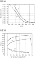
- FIG. 15 shows the absorption in the multiple quantum well structure 213 of the re-emission region 21 for the embodiment of FIG Figure 2C (Curve a) and the embodiment of the FIG. 2A (Curve b) as a function of the wavelength ⁇ of the electromagnetic radiation generated in the active layer 11. It can be seen that the absorption for electromagnetic radiation in the wavelength range of 400 nm, that is in the UV range, is optimal. Preferably, therefore, electromagnetic radiation is generated from the UV region in the active layer 11.
- FIG. 3B shows the efficiency plotted against the number of quantum well layers in the multiple quantum well structure 213 on a plot.
- Curves a, b show the efficiency for the embodiments of FIGS characters 2C or 2A.
- the curves c and d show the proportion of unconverted pump radiation that still exits the system for the embodiments of the Figures 2C or 2A.
- there are still optical losses due to absorption which in the variant according to Figure 2C are higher than in the variant according to FIG. 2A , It can be seen that the efficiency increases with the number of quantum well layers 211 in the multiple quantum well structure 213.
- the monolithic structure as used in conjunction with the Figure 2C is described in more detail, has a higher efficiency than the structure of FIG. 2A in which silicon with a refractive index of approximately 1.4 is used as connecting material 30 for connecting first semiconductor body 10 and second semiconductor body 20.
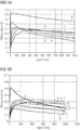
- the FIG. 4A shows graphically the efficiency vs. current at which the active region operates. It is internal efficiency without optical losses. Since the optical losses are not taken into account, the graphic plot of the FIG. 4A both to the embodiment of FIG. 2A as well as the embodiment of Figure 2C ,
- the curve a shows the efficiency for five optically pumped quantum well layers, the curve b for ten, the curve c for 20 and the curve f for 40 quantum well layers 211 in the multiple quantum well structure 213.
- the curve e shows the efficiency of the electrically pumped active region 11, the Generates UV radiation. Like from the FIG. 4A As can be seen, the internal efficiency increases for higher currents. For currents above 200 mA, all curves for optically pumped multiple quantum well structures are above the Efficiency for an electrically pumped quantum well structure as plotted in curve d.
- FIG. 4B Figure 12 is a graph of efficiency versus applied current taking into account optical losses.
- the dashed lines refer to monolithically integrated embodiments, as in connection with the Figure 2C are shown.
- the solid lines refer to embodiments in which first semiconductor body 10 and second semiconductor body 20 are manufactured separately from one another, as used in conjunction with FIG FIG. 2A are described.
- As a general trend it can be seen that, due to the lower optical losses, the efficiency for monolithically integrated light-emitting diodes is improved. However, these are more expensive in their manufacturing process.
- the curve a shows the efficiency of an electrically pumped active region with a single quantum well layer producing green light for comparison.
- Curve b shows the situation for five quantum well layers, the curve c for ten quantum well layers, the curve d for 20 quantum well layers and the curve e for 40 quantum well layers, each with silicon as the bonding material 30 between the first semiconductor body 10 and the second semiconductor body 20.
- the curve f shows the situation for five quantum well layers, the curve g for ten quantum well layers, the curve h for 20 quantum well layers and the curve i for 40 quantum well layers in the case where the first semiconductor body 10 and the second semiconductor body are monolithically integrated with each other.
- the light emitting diode from a number of about 20 optically pumped Quantum well layers 211 in the re-emission region 21 has a higher efficiency than the electrically pumped quantum well layer.
- the invention is not limited by the description based on the embodiments of these. Rather, the invention includes any combination of features in the claims.
Landscapes
- Engineering & Computer Science (AREA)
- Microelectronics & Electronic Packaging (AREA)
- Power Engineering (AREA)
- Computer Hardware Design (AREA)
- Manufacturing & Machinery (AREA)
- Physics & Mathematics (AREA)
- Condensed Matter Physics & Semiconductors (AREA)
- General Physics & Mathematics (AREA)
- Led Devices (AREA)
Description
Es wird eine Leuchtdiode angegeben.A light-emitting diode is specified.
Es wurde festgestellt, dass die interne Effizienz bei der Erzeugung von elektromagnetischer Strahlung für Leuchtdioden, die beispielsweise auf dem Materialsystem InGaN basieren, mit größer werdender Wellenlänge der erzeugten elektromagnetischen Strahlung von zirka 80 % bei einer Wellenlänge von 400 nm auf zirka 30 % bei einer Wellenlänge von 540 nm absinkt. Das heißt, die interne Effizienz für Leuchtdioden, die geeignet sind, grünes Licht zu erzeugen, ist im Vergleich zu Leuchtdioden, welche Strahlung aus dem UV-Bereich oder blaues Licht emittieren, sehr gering.It has been found that the internal efficiency in the generation of electromagnetic radiation for light-emitting diodes, which are based for example on the material system InGaN, with increasing wavelength of the generated electromagnetic radiation from about 80% at a wavelength of 400 nm to about 30% at one wavelength of 540 nm decreases. That is, the internal efficiency for light emitting diodes capable of producing green light is very small compared to light emitting diodes emitting ultraviolet or blue light.
Eine Möglichkeit, um die interne Effizienz von Leuchtdioden zu erhöhen, die geeignet sind, grünes Licht abzustrahlen, könnte nun darin bestehen, die Zahl der elektrisch gepumpten Quantentöpfe zu erhöhen. Es hat sich jedoch gezeigt, dass diesem Ansatz zur Lösung des beschriebenen Problems aufgrund der ungleichmäßigen Ladungsträgerverteilung im elektrischen Betrieb der Leuchtdiode enge Grenzen gesetzt sind. Nach derzeitigem Kenntnisstand können bei grünes Licht emittierenden InGaN-basierten Leuchtdioden maximal zwei Quantentöpfe vollständig bestromt werden, das Hinzufügen von weiteren Quantentöpfen scheint keinen positiven Einfluss auf die interne Effizienz der Leuchtdiode zu haben.One way to increase the internal efficiency of light emitting diodes capable of emitting green light could now be to increase the number of electrically pumped quantum wells. However, it has been found that this approach to solve the problem described due to the uneven charge carrier distribution in the electrical operation of the LED are narrow limits. According to the current state of knowledge, a maximum of two quantum wells can be completely energized with InGaN-based light-emitting diodes emitting green light; the addition of further quantum wells does not appear to have a positive influence on the internal efficiency of the light-emitting diode.
In der
In der
Eine zu lösende Aufgabe besteht darin, eine Leuchtdiode anzugeben, mit der elektromagnetische Strahlung besonders effizient erzeugt werden kann. Eine weitere zu lösende Aufgabe besteht darin, eine Leuchtdiode anzugeben, mit der insbesondere grünes Licht besonderes effizient erzeugt werden kann.An object to be solved is to specify a light-emitting diode with which electromagnetic radiation can be generated particularly efficiently. Another object to be solved is to provide a light-emitting diode with which, in particular, green light can be generated particularly efficiently.
Die Leuchtdiode umfasst einen ersten Halbleiterkörper. Der Halbleiterkörper ist beispielsweise epitaktisch gewachsen und kann auf dem InGaN-Materialsystem basieren. Der Halbleiterkörper umfasst zumindest einen aktiven Bereich, der elektrisch kontaktiert ist. Im Betrieb der Leuchtdiode wird im aktiven Bereich des ersten Halbleiterkörpers elektromagnetische Strahlung eines ersten Wellenlängenbereichs erzeugt. Die elektromagnetische Strahlung wird dabei mittels eines elektrischen Betreibens des aktiven Bereichs erzeugt. Bei der elektromagnetischen Strahlung des ersten Wellenlängenbereichs handelt es sich beispielsweise um elektromagnetische Strahlung aus dem UV-Bereich und/oder um blaues Licht.The light-emitting diode comprises a first semiconductor body. For example, the semiconductor body has grown epitaxially and may be based on the InGaN material system. The semiconductor body comprises at least one active region, which is electrically contacted. During operation of the light-emitting diode, electromagnetic radiation of a first wavelength range is generated in the active region of the first semiconductor body. The electromagnetic radiation is generated by means of an electrical operation of the active region. The electromagnetic radiation of the first wavelength range is, for example, electromagnetic radiation from the UV range and / or blue light.
Weiterhin umfasst die Leuchtdiode einen zweiten Halbleiterkörper, der an einer Oberseite des ersten Halbleiterkörpers am ersten Halbleiterkörper befestigt ist. Auch der zweite Halbleiterkörper ist vorzugsweise epitaktisch hergestellt. Der zweite Halbleiterkörper kann auf dem InGaN-Materialsystem oder dem InGaAlP-Materialsystem basieren. Der zweite Halbleiterkörper umfasst einen Re-Emissionsbereich mit einer Mehrfachquantentopfstruktur. Die Bezeichnung Quantentopfstruktur entfaltet dabei keine Bedeutung hinsichtlich der Dimensionalität der Quantisierung. Sie umfasst unter anderem Quantentröge, Quantendrähte und Quantenpunkte sowie jede Kombination der genannten Strukturen.Furthermore, the light-emitting diode comprises a second semiconductor body, which is fastened to an upper side of the first semiconductor body on the first semiconductor body. Also, the second semiconductor body is preferably produced epitaxially. The second semiconductor body may be based on the InGaN material system or the InGaAlP material system. The second semiconductor body comprises a re-emission region having a multiple quantum well structure. The name Quantum well structure has no significance with regard to the dimensionality of the quantization. It includes quantum wells, quantum wires and quantum dots, as well as any combination of these structures.
Im Betrieb der Leuchtdiode wird im Re-Emissionsbereich elektromagnetische Strahlung des ersten Wellenlängenbereichs absorbiert und elektromagnetische Strahlung eines zweiten Wellenlängenbereichs re-emittiert. Der zweite Wellenlängenbereich umfasst dabei bevorzugt elektromagnetische Strahlung, mit größeren Wellenlängen als der erste Wellenlängenbereich. Der zweite Wellenlängenbereich umfasst insbesondere elektromagnetische Strahlung aus dem Wellenlängenbereich von grünem und/oder gelbem und/oder rotem Licht.During operation of the light-emitting diode, electromagnetic radiation of the first wavelength range is absorbed in the re-emission range and re-emitted electromagnetic radiation of a second wavelength range. The second wavelength range preferably comprises electromagnetic radiation having longer wavelengths than the first wavelength range. In particular, the second wavelength range comprises electromagnetic radiation from the wavelength range of green and / or yellow and / or red light.
Insbesondere im Hinblick auf einen zweiten Halbleiterkörper, der auf InGaAlP basiert, ergibt sich der Vorteil, dass zum einen auf absorbierende Stromspreizungsschichten und elektrische Kontakte verzichtet werden kann. Zum anderen kann der thermisch aktivierte Verluststrom über eine Passivierung der dem ersten Halbleiterkörper zugewandten Oberfläche vermindert werden und damit die Temperaturabhängigkeit der Effizienz verringert werden.In particular with regard to a second semiconductor body based on InGaAlP, there is the advantage that, on the one hand, absorbing current spreading layers and electrical contacts can be dispensed with. On the other hand, the thermally activated leakage current can be reduced via a passivation of the surface facing the first semiconductor body and thus the temperature dependence of the efficiency can be reduced.
Der zweite Halbleiterkörper ist also vorzugsweise derart angeordnet, dass elektromagnetische Strahlung des ersten Wellenlängenbereichs aus dem ersten Halbleiterkörper in den zweiten Halbleiterkörper eintreten kann. Der zweite Halbleiterkörper ist dazu vorzugsweise auf einer Strahlungsaustrittsfläche des ersten Halbleiterkörpers angeordnet. Ein Großteil der im ersten Halbleiterkörper erzeugten elektromagnetischen Strahlung tritt in den zweiten Halbleiterkörper ein. Unter einem Großteil der elektromagnetischen Strahlung werden dabei wenigstens 50 %, vorzugsweise wenigstens 70 %, besonders bevorzugt wenigstens 85 % der elektromagnetischen Strahlung des ersten Wellenlängenbereichs verstanden. Der zweite Halbleiterkörper ist dazu besonders großflächig ausgeführt und bedeckt vorzugsweise die gesamte Strahlungsaustrittsfläche an der Oberseite des ersten Halbleiterkörpers. Beispielsweise schließen erster und zweiter Halbleiterkörper in lateraler Richtung bündig miteinander ab oder der zweite Halbleiterkörper überragt den ersten Halbleiterkörper in lateraler Richtung. Die laterale Richtung ist dabei jene Richtung, die beispielsweise zu einer epitaktischen Wachstumsrichtung des ersten Halbleiterkörpers senkrecht steht oder die parallel zu einer Schicht des ersten beziehungsweise des zweiten Halbleiterkörpers verläuft.The second semiconductor body is therefore preferably arranged such that electromagnetic radiation of the first wavelength range can enter from the first semiconductor body into the second semiconductor body. For this purpose, the second semiconductor body is preferably arranged on a radiation exit surface of the first semiconductor body. A majority of the electromagnetic radiation generated in the first semiconductor body enters the second Semiconductor body. A large part of the electromagnetic radiation is understood to be at least 50%, preferably at least 70%, particularly preferably at least 85% of the electromagnetic radiation of the first wavelength range. The second semiconductor body is designed to be particularly large area and preferably covers the entire radiation exit surface at the top of the first semiconductor body. By way of example, the first and second semiconductor bodies terminate flush with one another in the lateral direction, or the second semiconductor body projects beyond the first semiconductor body in the lateral direction. The lateral direction is that direction which, for example, is perpendicular to an epitaxial growth direction of the first semiconductor body or which runs parallel to a layer of the first or the second semiconductor body.
Ein Verbindungsmaterial ist zwischen dem ersten und dem zweiten Halbleiterkörper angeordnet, wobei das Verbindungsmaterial den ersten und den zweiten Halbleiterkörper mechanisch miteinander verbindet.A connection material is arranged between the first and the second semiconductor body, wherein the connection material mechanically connects the first and the second semiconductor body to one another.
Bei dem Verbindungsmaterial kann es sich beispielsweise um ein Halbleitermaterial handeln, aus dem der erste und der zweite Halbleiterkörper gebildet sind. Erster und zweiter Halbleiterkörper sind dann monolithisch miteinander integriert.The connecting material may be, for example, a semiconductor material, from which the first and the second semiconductor body are formed. First and second semiconductor body are then monolithically integrated with each other.
Erster und zweiter Halbleiterkörper sind in diesem Fall beispielsweise in einem einzigen epitaktischen Wachstumsprozess hergestellt und damit einstückig ausgebildet. Ferner ist es möglich, dass erster und zweiter Halbleiterkörper durch einen Waferbond-Prozess miteinander verbunden sind. Bei dem Waferbond-Prozess handelt es sich zum Beispiel um ein direktes Bonden (direct bonding) oder ein anodisches Bonden. Die einander zugewandten Oberflächen der beiden Halbleiterkörper weisen dabei keine Aufrauung auf und werden gegebenenfalls vor dem Verbinden jeweils geglättet.First and second semiconductor body are in this case, for example, produced in a single epitaxial growth process and thus integrally formed. Furthermore, it is possible for the first and second semiconductor bodies to be joined together by a wafer bonding process are connected. The wafer bonding process is, for example, a direct bonding or anodic bonding. The mutually facing surfaces of the two semiconductor bodies have no roughening and are optionally smoothed before joining.
Alternativ ist es möglich, dass es sich bei dem Verbindungsmaterial um ein transparentes, elektrisch leitfähiges Material handelt. Beispielsweise kann es sich bei dem Verbindungsmaterial dann um ein TCO (Transparent Conductive Oxide) -Material handeln. Erster und zweiter Halbleiterkörper können in diesem Fall beispielsweise über anodisches oder direktes Bonden mittels des Verbindungsmaterials miteinander verbunden sein.Alternatively, it is possible that the bonding material is a transparent, electrically conductive material. For example, the bonding material may then be a TCO (Transparent Conductive Oxide) material. In this case, first and second semiconductor bodies can be connected to one another, for example, by anodic or direct bonding by means of the connecting material.
Ferner ist es alternativ möglich, dass das Verbindungsmaterial elektrisch isolierend ist. Bei dem Verbindungsmaterial kann es sich dann beispielsweise um ein Silikon, ein hoch-brechendes Silikon mit einem Brechungsindex von größer 1,5, ein Epoxidharz, ein Siliziumoxid oder ein Siliziumnitrid handeln. Erster und zweiter Halbleiterkörper können mittels des Verbindungsmaterials dann durch Kleben oder Bonden miteinander verbunden sein.Furthermore, it is alternatively possible that the connecting material is electrically insulating. The bonding material may then be, for example, a silicone, a high refractive index silicone having a refractive index greater than 1.5, an epoxy, a silicon oxide or a silicon nitride. First and second semiconductor bodies can then be connected together by means of the bonding material by gluing or bonding.
Bei der beschriebenen Leuchtdiode ist der Re-Emissionsbereich des zweiten Halbleiterkörpers vorzugsweise nicht elektrisch kontaktiert. Das heißt, elektromagnetische Strahlung im Re-Emissionsbereich, das heißt die elektromagnetische Strahlung des zweiten Wellenlängenbereichs, wird nicht durch ein elektrisches Betreiben der Mehrfachquantentopfstruktur im Re-Emissionsbereich, sondern durch ein optisches Betreiben erzeugt. Das heißt, der Leuchtdiode liegt unter anderem die Erkenntnis zugrunde, dass wenn die Mehrfachquantentopfstruktur nicht elektrisch, sondern optisch gepumpt wird, eine gleichmäßige Ladungsverteilung in der Mehrfachquantentopfstruktur ermöglicht ist. Durch die direkte Anordnung des ersten Halbleiterkörpers, der kurzwelligere elektromagnetische Strahlung im Betrieb erzeugt mit dem zweiten Halbleiterkörper, der langwelligere elektromagnetische Strahlung im Betrieb erzeugt, ist es möglich, einen maximalen Anteil der elektromagnetischen Strahlung des ersten Wellenlängenbereichs für die gleichmäßige Erzeugung von Elektronen-Lochpaaren in der Mehrfachquantentopfstruktur des Re-Emissionsbereichs zu nutzen. Ferner zeichnet sich eine solche Leuchtdiode durch besonders gute spektrale und thermische Eigenschaften aus. Das heißt, der aktive Bereich des ersten Halbleiterkörpers kann beispielsweise besonders gut gekühlt werden, da der zweite Halbleiterkörper als eine Art Wärmespreizer für den ersten Halbleiterkörper wirkt.In the light-emitting diode described, the re-emission region of the second semiconductor body is preferably not electrically contacted. That is, electromagnetic radiation in the re-emission region, that is, the electromagnetic radiation of the second wavelength range, is not generated by electrically driving the multiple quantum well structure in the re-emission region but by optical driving. That is, the light-emitting diode is based inter alia on the knowledge that if the multiple quantum well structure not electrically, but optically pumped, a uniform charge distribution in the Mehrfachquantentopfstruktur is possible. Due to the direct arrangement of the first semiconductor body, which produces short-wave electromagnetic radiation in operation with the second semiconductor body, which generates longer wavelength electromagnetic radiation during operation, it is possible to use a maximum portion of the electromagnetic radiation of the first wavelength range for the uniform generation of electron-hole pairs in to use the multiple quantum well structure of the re-emission region. Furthermore, such a light-emitting diode is characterized by particularly good spectral and thermal properties. That is, the active region of the first semiconductor body can be cooled particularly well, for example, because the second semiconductor body acts as a kind of heat spreader for the first semiconductor body.
Der erste Halbleiterkörper weist an seiner dem zweiten Halbleiterkörper zugewandten Oberseite eine Vielzahl von Auskoppelstrukturen auf. Bei den Auskoppelstrukturen kann es sich beispielsweise um pyramidenförmige oder pyramidenstumpfförmige Erhebungen an der Oberseite des ersten Halbleiterkörpers handeln. Die Auskoppelstrukturen sind mit einem Material gebildet, das vom Material des ersten Halbleiterkörpers verschieden ist. Dabei handelt es sich bei den Auskoppelstrukturen um zusätzliche Strukturen. Die Auskoppelstrukturen bestehen vorzugsweise aus einem Material, dessen optischer Brechungsindex vom Brechungsindex des ersten Halbleiterkörpers um höchstens 30 % abweicht.The first semiconductor body has a plurality of coupling-out structures on its upper side facing the second semiconductor body. The coupling-out structures may be, for example, pyramidal or truncated pyramidal elevations on the upper side of the first semiconductor body. The coupling-out structures are formed with a material that is different from the material of the first semiconductor body. The decoupling structures are additional structures. The coupling-out structures are preferably made of a material whose optical refractive index deviates from the refractive index of the first semiconductor body by at most 30%.
Das Verbindungsmaterial umschließt die Auskoppelstrukturen an ihren freiliegenden Außenflächen. Das heißt, das Verbindungsmaterial ist zwischen den ersten und den zweiten Halbleiterkörper eingebracht und bedeckt die Auskoppelstrukturen. Das Verbindungsmaterial kann die Auskoppelstrukturen dann an den freiliegenden Außenflächen der Auskoppelstrukturen vollständig bedecken, so dass die Auskoppelstrukturen in das Verbindungsmaterial eingebettet sind. Es ist dann möglich, dass die Auskoppelstrukturen an der Oberseite des ersten Halbleiterkörpers den zweiten Halbleiterkörper nicht berühren, sondern dass zwischen den Auskoppelstrukturen und dem zweiten Halbleiterkörper Verbindungsmaterial angeordnet ist.The bonding material encloses the coupling-out structures on their exposed outer surfaces. That is, the bonding material is between the first and the second Semiconductor body introduced and covers the coupling-out. The connecting material can then completely cover the coupling-out structures on the exposed outer surfaces of the coupling-out structures, so that the coupling-out structures are embedded in the connecting material. It is then possible for the coupling-out structures on the upper side of the first semiconductor body not to touch the second semiconductor body, but for connecting material to be arranged between the coupling-out structures and the second semiconductor body.
Insgesamt ermöglichen es die Auskoppelstrukturen, dass elektromagnetische Strahlung des ersten Wellenlängenbereichs mit einer größeren Wahrscheinlichkeit aus dem ersten Halbleiterkörper austreten und in den zweiten Halbleiterkörper eintreten kann, als dies ohne die Auskoppelstrukturen der Fall wäre. Die Auskoppelstrukturen sorgen beispielsweise dafür, dass die Wahrscheinlichkeit für eine Totalreflexion der elektromagnetischen Strahlung aus dem ersten Wellenlängenbereich an der Grenzfläche zwischen erstem Halbleiterkörper und zweitem Halbleiterkörper reduziert ist.Overall, the coupling-out structures make it possible for electromagnetic radiation of the first wavelength range to emerge from the first semiconductor body with a greater probability and to enter the second semiconductor body than would be the case without the coupling-out structures. The coupling-out structures ensure, for example, that the probability of a total reflection of the electromagnetic radiation from the first wavelength range at the interface between the first semiconductor body and the second semiconductor body is reduced.
Gemäß zumindest einer Ausführungsform der Leuchtdiode weist der zweite Halbleiterkörper an seiner dem ersten Halbleiterkörper abgewandten Oberseite und/oder seiner dem ersten Halbleiterkörper zugewandten Unterseite eine Vielzahl von Auskoppelstrukturen auf. Die Auskoppelstrukturen können gleich oder unterschiedlich zu den Auskoppelstrukturen des ersten Halbleiterkörpers ausgebildet sein. Das heißt, die Auskoppelstrukturen können aus dem Material des zweiten Halbleiterkörpers strukturiert sein und damit aus dem Material des zweiten Halbleiterkörpers bestehen. Es ist jedoch auch möglich, dass die Auskoppelstrukturen aus einem Material bestehen, das vom Material des zweiten Halbleiterkörpers verschieden ist.In accordance with at least one embodiment of the light-emitting diode, the second semiconductor body has a multiplicity of coupling-out structures on its upper side facing away from the first semiconductor body and / or its underside facing the first semiconductor body. The coupling-out structures can be identical or different from the coupling-out structures of the first semiconductor body. That is, the coupling-out structures can be structured from the material of the second semiconductor body and thus consist of the material of the second semiconductor body. However, it is also possible that the coupling-out of a material exist, which is different from the material of the second semiconductor body.
Bevorzugt weist der zweite Halbleiterkörper an seiner dem ersten Halbleiterkörper abgewandten Oberseite und seiner dem ersten Halbleiterkörper zugewandten Unterseite eine Vielzahl von Auskoppelstrukturen auf. Die Auskoppelstrukturen an der Unterseite des zweiten Halbleiterkörpers verringern vorteilhaft Fresnel-Verluste am Interface zwischen zweitem Halbleiterkörper und Verbindungsmaterial.The second semiconductor body preferably has a multiplicity of outcoupling structures on its upper side facing away from the first semiconductor body and its underside facing the first semiconductor body. The coupling-out structures on the underside of the second semiconductor body advantageously reduce Fresnel losses at the interface between the second semiconductor body and connecting material.
Die Auskoppelstrukturen des zweiten Halbleiterkörpers bestehen in einer Ausführungsform aus einem Material, dessen optischer Brechungsindex vom optischen Brechungsindex des zweiten Halbleiterkörpers um höchstens 30 % abweicht.In one embodiment, the coupling-out structures of the second semiconductor body consist of a material whose optical refractive index deviates from the optical refractive index of the second semiconductor body by at most 30%.
Die Auskoppelstrukturen des zweiten Halbleiterkörpers erhöhen die Wahrscheinlichkeit für einen Lichtaustritt aus dem zweiten Halbleiterkörper heraus.The coupling-out structures of the second semiconductor body increase the probability of a light exit from the second semiconductor body.
Bei dem austretenden Licht kann es sich dabei um elektromagnetische Strahlung aus dem ersten oder dem zweiten Wellenlängenbereich handeln. Das heißt, die Leuchtdiode kann Mischlicht aus dem ersten und dem zweiten Wellenlängenbereich abstrahlen. Bei dem Mischlicht kann es sich zum Beispiel um weißes Licht handeln.The exiting light may be electromagnetic radiation from the first or the second wavelength range. That is, the light emitting diode can emit mixed light of the first and the second wavelength range. The mixed light may be, for example, white light.
Es ist aber auch möglich, dass die Leuchtdiode überwiegend elektromagnetische Strahlung aus dem zweiten Wellenlängenbereich abstrahlt. Das heißt, der überwiegende Teil - zum Beispiel wenigstens 90 % - der elektromagnetischen Strahlung aus dem ersten Wellenlängenbereich, die in den zweiten Halbleiterkörper eingetreten ist, wird im zweiten Halbleiterkörper absorbiert. Auf diese Weise ist es möglich, dass die Leuchtdiode beispielsweise farbreines grünes, gelbes oder rotes Licht emittiert.But it is also possible that the LED predominantly emits electromagnetic radiation from the second wavelength range. That is, the majority - for example, at least 90% - of the electromagnetic radiation from the first wavelength range that has entered the second semiconductor body is in the second Semiconductor body absorbed. In this way, it is possible that the light-emitting diode emits, for example, pure green, yellow or red light.
Gemäß zumindest einer Ausführungsform der Leuchtdiode enthält oder besteht das Material der Auskoppelstrukturen des ersten und/oder des zweiten Halbleiterkörpers aus einem der folgenden Stoffe: Titanoxid, Zinkselenid, Aluminiumnitrid, Siliziumcarbid, Bornitrid und/oder Tantaloxid. Diese Stoffe zeichnen sich dadurch aus, dass sie einen optischen Brechungsindex aufweisen, der um höchstens 30 % vom Brechungsindex eines InGaN-basierten Halbleiterkörpers abweichen.According to at least one embodiment of the light-emitting diode, the material of the coupling-out structures of the first and / or the second semiconductor body contains or consists of one of the following substances: titanium oxide, zinc selenide, aluminum nitride, silicon carbide, boron nitride and / or tantalum oxide. These substances are distinguished by the fact that they have an optical refractive index which deviates by at most 30% from the refractive index of an InGaN-based semiconductor body.
Gemäß zumindest einer Ausführungsform der Leuchtdiode ist eine Spiegelschicht an der dem zweiten Halbleiterkörper abgewandten Unterseite des ersten Halbleiterkörpers befestigt. Bei der Spiegelschicht handelt es sich beispielsweise um einen dielektrischen Spiegel, einen Bragg-Spiegel, einen metallischen Spiegel oder um eine Kombination der genannten Spiegel. Die Spiegelschicht ist vorgesehen, elektromagnetische Strahlung des ersten Wellenlängenbereichs in Richtung des zweiten Halbleiterkörpers zu reflektieren. Auf diese Weise ist es ermöglicht, dass ein besonders großer Anteil der elektromagnetischen Strahlung des ersten Wellenlängenbereichs in den zweiten Halbleiterkörper eintritt. Ferner kann die Spiegelschicht auch elektromagnetische Strahlung des zweiten Wellenlängenbereichs, die aus dem zweiten Halbleiterkörper in Richtung des ersten Halbleiterkörpers abgestrahlt wird, in Richtung des zweiten Halbleiterkörpers und damit aus der Leuchtdiode hinaus reflektieren.In accordance with at least one embodiment of the light-emitting diode, a mirror layer is fastened to the underside of the first semiconductor body facing away from the second semiconductor body. The mirror layer is, for example, a dielectric mirror, a Bragg mirror, a metallic mirror or a combination of said mirrors. The mirror layer is provided to reflect electromagnetic radiation of the first wavelength range in the direction of the second semiconductor body. In this way, it is possible for a particularly large proportion of the electromagnetic radiation of the first wavelength range to enter the second semiconductor body. Furthermore, the mirror layer can also reflect electromagnetic radiation of the second wavelength range, which is emitted from the second semiconductor body in the direction of the first semiconductor body, in the direction of the second semiconductor body and thus out of the light-emitting diode.
Gemäß zumindest einer Ausführungsform der Leuchtdiode umfasst die Mehrfachquantenstruktur des Re-Emissionsbereichs wenigstens 20 Quantentopfschichten. Die Quantentopfschichten sind beispielsweise entlang einer Wachstumsrichtung des zweiten Halbleiterkörpers übereinander angeordnet und durch Barriereschichten voneinander getrennt. Es hat sich dabei gezeigt, dass eine so große Anzahl von Quantentopfschichten mittels optischen Pumpens gleichmäßig mit Ladungsträgern besetzt werden kann und sich die Effizienz der Erzeugung von elektromagnetischer Strahlung des zweiten Wellenlängenbereichs aufgrund der hohen Anzahl von Quantentopfschichten merklich erhöht. Insbesondere bei der Vollkonversion von blauem Licht oder UV-Strahlung zu grünem Licht ist die Zahl der Quantentopfschichten (auch Quantenfilme) wichtig für die Effizienz der Lichterzeugung, da Photonen nur in den Quantentopfschichten absorbiert werden und bei einer hohen Zahl von Quantentopfschichten ein ausreichender Absorptionsquerschnitt gegeben ist. Des Weiteren ergibt sich bei einer hohen Anzahl von Quantentopfschichten aufgrund der geringeren Ladungsträgerdichte in den einzelnen Töpfen eine vorteilhafte Verschiebung des Effizienz-Maximums zu höheren Strömen. Daher kann die Vollkonversion bei hohen Stromdichten von > 100 A/cm2 effizienter als eine direkt elektrisch gepumpte grüne Leuchtdiode sein.In accordance with at least one embodiment of the light emitting diode, the multiple quantum structure of the re-emission region comprises at least 20 quantum well layers. The quantum well layers are arranged, for example, one above the other along a growth direction of the second semiconductor body and separated from one another by barrier layers. It has been found that such a large number of quantum well layers can be uniformly filled with carriers by optical pumping and the efficiency of generation of electromagnetic radiation of the second wavelength range is markedly increased due to the large number of quantum well layers. Especially in the case of full conversion of blue light or UV radiation to green light, the number of quantum well layers (also quantum films) is important for the efficiency of light generation, since photons are absorbed only in the quantum well layers and a sufficient absorption cross section is given for a large number of quantum well layers , Furthermore, given a high number of quantum well layers, an advantageous shift of the maximum efficiency to higher currents results due to the lower charge carrier density in the individual pots. Therefore, full conversion at high current densities of> 100 A / cm 2 can be more efficient than a directly electrically pumped green LED.
Im Folgenden wird die hier beschriebene Leuchtdiode anhand von Ausführungsbeispielen und den dazugehörigen Figuren näher erläutert.
- Die Figuren 1A und 1B
- zeigen anhand graphischer Auftragungen die Effizienz von elektrisch betriebenen blauen und grünen Leuchtdioden.
- Mit den Figuren 2A, 2B, 2C und 2D
- sind anhand schematischer Schnittdarstellungen Ausführungsbeispiele von hier beschriebenen Leuchtdioden näher erläutert.
- Anhand der graphischen Auftragungen der Figuren 3A, 3B, 4A, 4B
- sind Eigenschaften von hier beschriebenen Leuchtdioden näher erläutert.
- Figures 1A and 1B
- graphically show the efficiency of electrically driven blue and green LEDs.
- With the figures 2A, 2B, 2C and 2D
- are explained in more detail with reference to schematic sectional views of embodiments of light-emitting diodes described herein.
- With reference to the graphs of Figures 3A, 3B, 4A, 4B
- Properties of light-emitting diodes described here are explained in more detail.
Gleiche, gleichartige oder gleich wirkende Elemente sind in den Figuren mit denselben Bezugszeichen versehen. Die Figuren und die Größenverhältnisse der in den Figuren dargestellten Elemente untereinander sind nicht als maßstäblich zu betrachten. Vielmehr können einzelne Elemente zur besseren Darstellbarkeit und/oder zum besseren Verständnis übertrieben groß dargestellt sein.The same, similar or equivalent elements are provided in the figures with the same reference numerals. The figures and the proportions of the elements shown in the figures with each other are not to be considered to scale. Rather, individual elements may be exaggerated in size for better representability and / or better understanding.
Die
Die
Insgesamt sind elektrisch gepumpte grüne Leuchtdioden elektrisch gepumpten blauen Leuchtdioden oder UV-Strahlung emittierenden Leuchtdioden bezüglich ihrer Effizienz unterlegen.Overall, electrically pumped green light emitting diodes are inferior in their efficiency to electrically pumped blue light emitting diodes or UV emitting light emitting diodes.
Die
Der erste Halbleiterkörper 10 umfasst einen p-dotierten Bereich 12 und einen n-dotierten Bereich 13. Zwischen dem p-dotierten Bereich 12 und dem n-dotierten Bereich 13 ist der aktive Bereich 11 angeordnet. Der aktive Bereich 11 wird elektrisch betrieben, die elektrischen Anschlüsse sind in der
Der zweite Halbleiterkörper 20 umfasst einen n-dotierten Bereich 22, einen p-dotierten Bereich 23 und einen Re-Emissionsbereich 21, der zwischen den beiden Bereichen angeordnet ist. Der Re-Emissionsbereich 21 umfasst eine Mehrfachquantentopfstruktur. Der Re-Emissionsbereich 21 ist nicht elektrisch angeschlossen und wird nicht elektrisch betrieben.The
An seiner Oberseite 20a umfasst der zweite Halbleiterkörper 20 Auskoppelstrukturen 24, die vorliegend mittels KOH-Ätzung in den Halbleiterkörper 20 strukturiert sind. Auch die Auskoppelstrukturen 24 können aus anderen Materialien, wie sie weiter oben beschrieben sind, gebildet sein. Auch an der Unterseite 20b des zweiten Halbleiterkörpers 20 können Auskoppelstrukturen 24 angeordnet sein (in der Figur nicht gezeigt).On its
Zwischen erstem Halbleiterkörper 10 und zweitem Halbleiterkörper 20 ist ein Verbindungsmaterial 30 angeordnet, das vorliegend Silikon enthält oder aus Silikon besteht. Das Verbindungsmaterial 30 umschließt die Auskoppelstrukturen 14 des ersten Halbleiterkörpers 10 an ihren freiliegenden Außenflächen vollständig. Das Verbindungsmaterial 30 ist vorliegend elektrisch isolierend und stellt eine mechanische Verbindung zwischen den beiden Halbleiterkörpern dar.Between the
Erster Halbleiterkörper 10 und zweiter Halbleiterkörper 20 sind vorliegend getrennt voneinander epitaktisch hergestellt und nachträglich mittels des Verbindungsmaterials 30 miteinander verbunden. An ihren Seitenflächen 20c und 10c schließen zweiter Halbleiterkörper 20 und erster Halbleiterkörper 10 bündig miteinander ab, so dass sich die Halbleiterkörper 10, 20 gegenseitig lateral nicht überragen.
An der dem zweiten Halbleiterkörper 20 abgewandten Unterseite 10b des ersten Halbleiterkörpers 10 ist eine Spiegelschicht 40 angeordnet, die vorliegend als metallischer Spiegel ausgebildet ist, der beispielsweise aus Aluminium oder Silber besteht. Die Spiegelschicht 40 ist sowohl zur Reflexion von elektromagnetischer Strahlung 110 aus dem ersten Wellenlängenbereich und elektromagnetischer Strahlung 210 aus dem zweiten Wellenlängenbereich geeignet.Arranged on the
In der schematischen Schnittdarstellung der
In Verbindung mit der
Anhand der schematischen Schnittdarstellung 2D ist eine Möglichkeit zur elektrischen Kontaktierung des aktiven Bereichs 11 des ersten Halbleiterkörpers 10 schematisch erläutert. Von der Unterseite 10b des ersten Halbleiterkörpers 10 her sind vorliegend Kanäle 53 durch die Spiegelschicht hindurch in den Halbleiterkörper 10 eingebracht, die mit einem elektrisch leitenden Material gefüllt sind, das an der dem Halbleiterkörper 10 abgewandten Seite der Spiegelschicht 40 elektrische Kontaktstellen 51, 52 bildet. Neben der gezeigten Ausführungsform sind auch andere Anschlussmöglichkeit zur elektrischen Kontaktierung der aktiven Schicht 11 des ersten Halbleiterkörpers 10 denkbar.A possibility for electrical contacting of the
Die graphische Auftragung der
Die
Die
Die
Die Kurve a zeigt die Effizienz eines elektrisch gepumpten aktiven Bereichs mit einer einzigen Quantentopfschicht, der grünes Licht erzeugt zum Vergleich. Die Kurve b zeigt die Situation für fünf Quantentopfschichten, die Kurve c für zehn Quantentopfschichten, die Kurve d für 20 Quantentopfschichten und die Kurve e für 40 Quantentopfschichten, jeweils mit Silikon als Verbindungsmaterial 30 zwischen erstem Halbleiterkörper 10 und zweitem Halbleiterkörper 20.The curve a shows the efficiency of an electrically pumped active region with a single quantum well layer producing green light for comparison. Curve b shows the situation for five quantum well layers, the curve c for ten quantum well layers, the curve d for 20 quantum well layers and the curve e for 40 quantum well layers, each with silicon as the
Die Kurve f zeigt die Situation für fünf Quantentopfschichten, die Kurve g für zehn Quantentopfschichten, die Kurve h für 20 Quantentopfschichten und die Kurve i für 40 Quantentopfschichten für den Fall, dass erster Halbleiterkörper 10 und zweiter Halbleiterkörper monolithisch miteinander integriert sind. Insgesamt weist die Leuchtdiode ab einer Zahl von zirka 20 optisch gepumpten Quantentopfschichten 211 im Re-Emissionsbereich 21 eine höhere Effizienz als die elektrisch gepumpte Quantentopfschicht auf. Die Erfindung ist nicht durch die Beschreibung anhand der Ausführungsbeispiele auf diese beschränkt. Vielmehr umfasst die Erfindung jede Kombination von Merkmalen in den Patentansprüchen.The curve f shows the situation for five quantum well layers, the curve g for ten quantum well layers, the curve h for 20 quantum well layers and the curve i for 40 quantum well layers in the case where the
Diese Patentanmeldung beansprucht die Prioritäten der
Claims (13)
- Light-emitting diode comprising- a first semiconductor body (10), which comprises at least one active region (11) which is electrically contact-connected, wherein electromagnetic radiation (110) in a first wavelength range is generated in the active region (11) during the operation of the light-emitting diode, and- a second semiconductor body (20), which is fixed to the first semiconductor body (10) at a top side (10a) of the first semiconductor body (10), wherein the second semiconductor body (20) has a re-emission region (21) with a multiple quantum well structure (213), and wherein electromagnetic radiation (110) in the first wavelength range is absorbed and electromagnetic radiation in a second wavelength range (220) is re-emitted in the re-emission region (21) during the operation of the light-emitting diode, and- a connecting material (30) arranged between the first (10) and second semiconductor body (20), wherein the connecting material (30) mechanically connects the first (10) and the second semiconductor body (20) to one another, wherein- the first semiconductor body (10) has a multiplicity of coupling-out structures (14) at its top side (10a) facing the second semiconductor body (20) characterized in that- the connecting material (30) encloses the coupling-out structures (14) at their exposed outer areas, and- the coupling-out structures (14) are formed with a material which is different from the material of the first semiconductor body (10).
- Light-emitting diode according to the preceding claim, wherein the connecting material (30) is electrically insulating.
- Light-emitting diode according to the preceding claim,
wherein the connecting material (30) is silicone or contains a silicone. - Light-emitting diode according to Claim 1,
wherein the coupling-out structures (14) consist of a material whose refractive index deviates by at most 30% from the refractive index of the first semiconductor body (10). - Light-emitting diode according to any of the preceding claims,
wherein the second semiconductor body (20) has a multiplicity of coupling-out structures (24) at its top side (20a) remote from the first semiconductor body and/or its underside (20b) facing the first semiconductor body. - Light-emitting diode according to the preceding claim,
wherein the coupling-out structures (24) consist of a material whose refractive index deviates by at most 30% from the refractive index of the second semiconductor body (20). - Light-emitting diode according to any of the preceding claims,
wherein the material of the coupling-out structures (14, 24) contains or consists of one of the following substances: TiO2, ZnS, AlN, SiC, BN, Ta2O5. - Light-emitting diode according to any of the preceding claims,
wherein a mirror layer (40) is fixed to the first semiconductor body (10) at the underside (10b) of the first semiconductor body (10) remote from the second semiconductor body (20). - Light-emitting diode according to any of the preceding claims,
wherein the coupling-out structures (24) are formed with a material which is different from the material of the first semiconductor body (10) and from the material of the second semiconductor body (20). - Light-emitting diode according to any of the preceding claims,
wherein the first wavelength range comprises electromagnetic radiation from the wavelength range of UV radiation and/or blue light. - Light-emitting diode according to the preceding claim,
wherein the second wavelength range comprises electromagnetic radiation from the wavelength range of green light. - Light-emitting diode according to any of the preceding claims,
wherein the multiple quantum well structure (213) of the re-emission region has at least 20 quantum well layers (211). - Light-emitting diode according to any of the preceding claims,
wherein the coupling-out structures (14) are pyramid-shaped elevations, or elevations in the shape of truncated pyramids, at the top side of the first semiconductor body (10).
Applications Claiming Priority (3)
| Application Number | Priority Date | Filing Date | Title |
|---|---|---|---|
| DE102009001844 | 2009-03-25 | ||
| DE102009020127A DE102009020127A1 (en) | 2009-03-25 | 2009-05-06 | led |
| PCT/EP2010/053304 WO2010108811A1 (en) | 2009-03-25 | 2010-03-15 | Light diode |
Publications (2)
| Publication Number | Publication Date |
|---|---|
| EP2412021A1 EP2412021A1 (en) | 2012-02-01 |
| EP2412021B1 true EP2412021B1 (en) | 2017-02-01 |
Family
ID=42664166
Family Applications (1)
| Application Number | Title | Priority Date | Filing Date |
|---|---|---|---|
| EP10710274.1A Active EP2412021B1 (en) | 2009-03-25 | 2010-03-15 | Light emitting diode |
Country Status (8)
| Country | Link |
|---|---|
| US (1) | US20120256161A1 (en) |
| EP (1) | EP2412021B1 (en) |
| JP (1) | JP2012521644A (en) |
| KR (1) | KR20110137814A (en) |
| CN (1) | CN102362348A (en) |
| DE (1) | DE102009020127A1 (en) |
| TW (1) | TWI520374B (en) |
| WO (1) | WO2010108811A1 (en) |
Families Citing this family (8)
| Publication number | Priority date | Publication date | Assignee | Title |
|---|---|---|---|---|
| US20130264588A1 (en) * | 2012-04-09 | 2013-10-10 | Phostek, Inc. | Compact led package |
| DE102015116595A1 (en) | 2015-09-30 | 2017-03-30 | Osram Opto Semiconductors Gmbh | Component with a light-emitting semiconductor chip |
| DE102016101442A1 (en) | 2016-01-27 | 2017-07-27 | Osram Opto Semiconductors Gmbh | Conversion element and radiation-emitting semiconductor device with such a conversion element |
| DE102016104280A1 (en) * | 2016-03-09 | 2017-09-14 | Osram Opto Semiconductors Gmbh | Component and method for manufacturing a device |
| DE102016113002B4 (en) | 2016-07-14 | 2022-09-29 | OSRAM Opto Semiconductors Gesellschaft mit beschränkter Haftung | Devices with improved efficiency and methods of manufacturing devices |
| FR3061605B1 (en) * | 2016-12-29 | 2019-05-31 | Aledia | Optoelectronic device with light-emitting diodes |
| DE102018124473A1 (en) | 2018-10-04 | 2020-04-09 | Osram Opto Semiconductors Gmbh | OPTOELECTRONIC COMPONENT, METHOD FOR CONTROLLING AN OPTOELECTRONIC COMPONENT AND LIGHTING DEVICE |
| JP7414419B2 (en) | 2019-07-30 | 2024-01-16 | キヤノン株式会社 | Light emitting device and method for manufacturing the light emitting device |
Family Cites Families (25)
| Publication number | Priority date | Publication date | Assignee | Title |
|---|---|---|---|---|
| JPH11135838A (en) * | 1997-10-20 | 1999-05-21 | Ind Technol Res Inst | White-color light-emitting diode and manufacture thereof |
| AU4557300A (en) * | 1999-04-27 | 2000-11-10 | Karandashov, Sergey | Radiation source |
| WO2000077861A1 (en) * | 1999-06-14 | 2000-12-21 | Augusto Carlos J R P | Stacked wavelength-selective opto-electronic device |
| CA2393081C (en) * | 1999-12-03 | 2011-10-11 | Cree Lighting Company | Enhanced light extraction in leds through the use of internal and external optical elements |
| TW497277B (en) * | 2000-03-10 | 2002-08-01 | Toshiba Corp | Semiconductor light emitting device and method for manufacturing the same |
| JP2004296219A (en) * | 2003-03-26 | 2004-10-21 | Fuji Photo Film Co Ltd | Light emitting element |
| US7009213B2 (en) * | 2003-07-31 | 2006-03-07 | Lumileds Lighting U.S., Llc | Light emitting devices with improved light extraction efficiency |
| DE10354936B4 (en) * | 2003-09-30 | 2012-02-16 | Osram Opto Semiconductors Gmbh | Radiation-emitting semiconductor component |
| DE102004004765A1 (en) * | 2004-01-29 | 2005-09-01 | Rwe Space Solar Power Gmbh | Active Zones Semiconductor Structure |
| JP2005252222A (en) * | 2004-02-03 | 2005-09-15 | Matsushita Electric Ind Co Ltd | Semiconductor light-emitting device, lighting module, lighting device, display device, and method of manufacturing semiconductor light-emitting device |
| US7808011B2 (en) * | 2004-03-19 | 2010-10-05 | Koninklijke Philips Electronics N.V. | Semiconductor light emitting devices including in-plane light emitting layers |
| DE102004052245A1 (en) * | 2004-06-30 | 2006-02-02 | Osram Opto Semiconductors Gmbh | Radiation emitting semiconductor chip e.g. luminescent diode chip, has reemission structure, and reemission layer formed for widening spectrums of chip against respective spectrum of radiation of peak wavelength |
| US7223998B2 (en) * | 2004-09-10 | 2007-05-29 | The Regents Of The University Of California | White, single or multi-color light emitting diodes by recycling guided modes |
| US7402831B2 (en) * | 2004-12-09 | 2008-07-22 | 3M Innovative Properties Company | Adapting short-wavelength LED's for polychromatic, broadband, or “white” emission |
| TWI267212B (en) * | 2004-12-30 | 2006-11-21 | Ind Tech Res Inst | Quantum dots/quantum well light emitting diode |
| JP4971672B2 (en) * | 2005-09-09 | 2012-07-11 | パナソニック株式会社 | Light emitting device |
| US7285791B2 (en) * | 2006-03-24 | 2007-10-23 | Goldeneye, Inc. | Wavelength conversion chip for use in solid-state lighting and method for making same |
| US20070284565A1 (en) * | 2006-06-12 | 2007-12-13 | 3M Innovative Properties Company | Led device with re-emitting semiconductor construction and optical element |
| KR20090016694A (en) * | 2006-06-12 | 2009-02-17 | 쓰리엠 이노베이티브 프로퍼티즈 컴파니 | Led device with re-emitting semiconductor construction and optical element |
| EP1887634A3 (en) * | 2006-08-11 | 2011-09-07 | OSRAM Opto Semiconductors GmbH | Semiconductor light emitting device |
| US9018619B2 (en) * | 2006-10-09 | 2015-04-28 | Cree, Inc. | Quantum wells for light conversion |
| TWI349371B (en) * | 2007-02-13 | 2011-09-21 | Epistar Corp | An optoelectronical semiconductor device having a bonding structure |
| JP2010541295A (en) * | 2007-10-08 | 2010-12-24 | スリーエム イノベイティブ プロパティズ カンパニー | Light emitting diode with semiconductor wavelength converter |
| JP2009099893A (en) * | 2007-10-19 | 2009-05-07 | Showa Denko Kk | Iii group nitride semiconductor light emitting device |
| CN101897038B (en) * | 2007-12-10 | 2012-08-29 | 3M创新有限公司 | Down-converted light emitting diode with simplified light extraction |
-
2009
- 2009-05-06 DE DE102009020127A patent/DE102009020127A1/en active Pending
-
2010
- 2010-03-15 KR KR1020117025033A patent/KR20110137814A/en not_active Application Discontinuation
- 2010-03-15 CN CN2010800129718A patent/CN102362348A/en active Pending
- 2010-03-15 EP EP10710274.1A patent/EP2412021B1/en active Active
- 2010-03-15 JP JP2012501239A patent/JP2012521644A/en active Pending
- 2010-03-15 US US13/260,562 patent/US20120256161A1/en not_active Abandoned
- 2010-03-15 WO PCT/EP2010/053304 patent/WO2010108811A1/en active Application Filing
- 2010-03-19 TW TW099108111A patent/TWI520374B/en active
Also Published As
| Publication number | Publication date |
|---|---|
| TWI520374B (en) | 2016-02-01 |
| EP2412021A1 (en) | 2012-02-01 |
| US20120256161A1 (en) | 2012-10-11 |
| JP2012521644A (en) | 2012-09-13 |
| KR20110137814A (en) | 2011-12-23 |
| WO2010108811A1 (en) | 2010-09-30 |
| TW201044634A (en) | 2010-12-16 |
| DE102009020127A1 (en) | 2010-09-30 |
| CN102362348A (en) | 2012-02-22 |
Similar Documents
| Publication | Publication Date | Title |
|---|---|---|
| EP2412021B1 (en) | Light emitting diode | |
| EP2193550B1 (en) | Radiation-emitting semiconductor body | |
| EP2638575B1 (en) | Optoelectronic semiconductor chip and method for producing the same | |
| EP2149163B9 (en) | Luminescence diode chip with an angle filter element | |
| EP2149160B1 (en) | Optoelectronic component and method for producing a plurality of optoelectronic components | |
| EP1277241B1 (en) | Gan-based light-emitting-diode chip | |
| DE102013112549B4 (en) | Process for the production of optoelectronic semiconductor components and optoelectronic semiconductor components | |
| DE202011110910U1 (en) | Light emitting diode chip | |
| DE102007029370A1 (en) | Semiconductor chip and method for producing a semiconductor chip | |
| WO2010124915A1 (en) | Light emitting diode and method for producing a light emitting diode | |
| DE102008009769A1 (en) | Double-flip semiconductor device and manufacturing method | |
| EP2273574B1 (en) | Method for producing a light emitting diode with a light emitting diode chip on a GaN basis | |
| WO2009076933A1 (en) | Radiation -emitting device | |
| WO2012013523A1 (en) | Radation-emitting semi-conductor chip and a method for producing a radiation-emitting semi-conductor chip | |
| WO2013057002A1 (en) | Optoelectronic semiconductor chip and method for producing the latter | |
| DE10246891A1 (en) | Structure for light-emitting diode comprises reflector separated from light-emitting region by predetermined spacing | |
| DE102011015726B4 (en) | Semiconductor chip, display with a plurality of semiconductor chips and method for their production | |
| EP2160773B1 (en) | Optoelectronic semiconductor chip | |
| WO2017129446A1 (en) | Conversion element, and radiation emitting semiconductor component comprising a conversion element of said type | |
| WO2017081181A1 (en) | Radiation-emitting semiconductor chip, optoelectronic component comprising a radiation-emitting semiconductor chip, and method for coating a radiation-emitting semiconductor chip | |
| WO2012100868A1 (en) | Optoelectronic semiconductor chip and method for producing same | |
| WO2019020424A1 (en) | Optoelectronic semiconductor chip, high voltage semiconductor chip and method for producing an optoelectronic semiconductor chip | |
| WO2019048370A1 (en) | Light-emitting semiconductor component | |
| DE102018108875A1 (en) | Optoelectronic component with passivation layer and method for producing the optoelectronic component | |
| DE112019002362B4 (en) | Optoelectronic semiconductor component with a first and a second current distribution structure |
Legal Events
| Date | Code | Title | Description |
|---|---|---|---|
| PUAI | Public reference made under article 153(3) epc to a published international application that has entered the european phase |
Free format text: ORIGINAL CODE: 0009012 |
|
| 17P | Request for examination filed |
Effective date: 20110608 |
|
| AK | Designated contracting states |
Kind code of ref document: A1 Designated state(s): AT BE BG CH CY CZ DE DK EE ES FI FR GB GR HR HU IE IS IT LI LT LU LV MC MK MT NL NO PL PT RO SE SI SK SM TR |
|
| DAX | Request for extension of the european patent (deleted) | ||
| 17Q | First examination report despatched |
Effective date: 20160607 |
|
| GRAP | Despatch of communication of intention to grant a patent |
Free format text: ORIGINAL CODE: EPIDOSNIGR1 |
|
| RIC1 | Information provided on ipc code assigned before grant |
Ipc: H01L 33/08 20100101ALN20160824BHEP Ipc: H01L 25/075 20060101AFI20160824BHEP Ipc: H01L 33/58 20100101ALN20160824BHEP Ipc: H01L 33/22 20100101ALN20160824BHEP Ipc: H01L 33/38 20100101ALN20160824BHEP Ipc: H01L 33/50 20100101ALN20160824BHEP |
|
| INTG | Intention to grant announced |
Effective date: 20160906 |
|
| GRAS | Grant fee paid |
Free format text: ORIGINAL CODE: EPIDOSNIGR3 |
|
| GRAA | (expected) grant |
Free format text: ORIGINAL CODE: 0009210 |
|
| AK | Designated contracting states |
Kind code of ref document: B1 Designated state(s): AT BE BG CH CY CZ DE DK EE ES FI FR GB GR HR HU IE IS IT LI LT LU LV MC MK MT NL NO PL PT RO SE SI SK SM TR |
|
| REG | Reference to a national code |
Ref country code: GB Ref legal event code: FG4D Free format text: NOT ENGLISH |
|
| REG | Reference to a national code |
Ref country code: CH Ref legal event code: EP Ref country code: AT Ref legal event code: REF Ref document number: 866205 Country of ref document: AT Kind code of ref document: T Effective date: 20170215 |
|
| REG | Reference to a national code |
Ref country code: IE Ref legal event code: FG4D Free format text: LANGUAGE OF EP DOCUMENT: GERMAN |
|
| REG | Reference to a national code |
Ref country code: DE Ref legal event code: R096 Ref document number: 502010013139 Country of ref document: DE |
|
| REG | Reference to a national code |
Ref country code: NL Ref legal event code: MP Effective date: 20170201 |
|
| REG | Reference to a national code |
Ref country code: LT Ref legal event code: MG4D |
|
| PG25 | Lapsed in a contracting state [announced via postgrant information from national office to epo] |
Ref country code: HR Free format text: LAPSE BECAUSE OF FAILURE TO SUBMIT A TRANSLATION OF THE DESCRIPTION OR TO PAY THE FEE WITHIN THE PRESCRIBED TIME-LIMIT Effective date: 20170201 Ref country code: IS Free format text: LAPSE BECAUSE OF FAILURE TO SUBMIT A TRANSLATION OF THE DESCRIPTION OR TO PAY THE FEE WITHIN THE PRESCRIBED TIME-LIMIT Effective date: 20170601 Ref country code: GR Free format text: LAPSE BECAUSE OF FAILURE TO SUBMIT A TRANSLATION OF THE DESCRIPTION OR TO PAY THE FEE WITHIN THE PRESCRIBED TIME-LIMIT Effective date: 20170502 Ref country code: NO Free format text: LAPSE BECAUSE OF FAILURE TO SUBMIT A TRANSLATION OF THE DESCRIPTION OR TO PAY THE FEE WITHIN THE PRESCRIBED TIME-LIMIT Effective date: 20170501 Ref country code: LT Free format text: LAPSE BECAUSE OF FAILURE TO SUBMIT A TRANSLATION OF THE DESCRIPTION OR TO PAY THE FEE WITHIN THE PRESCRIBED TIME-LIMIT Effective date: 20170201 Ref country code: FI Free format text: LAPSE BECAUSE OF FAILURE TO SUBMIT A TRANSLATION OF THE DESCRIPTION OR TO PAY THE FEE WITHIN THE PRESCRIBED TIME-LIMIT Effective date: 20170201 |
|
| PG25 | Lapsed in a contracting state [announced via postgrant information from national office to epo] |
Ref country code: PT Free format text: LAPSE BECAUSE OF FAILURE TO SUBMIT A TRANSLATION OF THE DESCRIPTION OR TO PAY THE FEE WITHIN THE PRESCRIBED TIME-LIMIT Effective date: 20170601 Ref country code: PL Free format text: LAPSE BECAUSE OF FAILURE TO SUBMIT A TRANSLATION OF THE DESCRIPTION OR TO PAY THE FEE WITHIN THE PRESCRIBED TIME-LIMIT Effective date: 20170201 Ref country code: BG Free format text: LAPSE BECAUSE OF FAILURE TO SUBMIT A TRANSLATION OF THE DESCRIPTION OR TO PAY THE FEE WITHIN THE PRESCRIBED TIME-LIMIT Effective date: 20170501 Ref country code: ES Free format text: LAPSE BECAUSE OF FAILURE TO SUBMIT A TRANSLATION OF THE DESCRIPTION OR TO PAY THE FEE WITHIN THE PRESCRIBED TIME-LIMIT Effective date: 20170201 Ref country code: LV Free format text: LAPSE BECAUSE OF FAILURE TO SUBMIT A TRANSLATION OF THE DESCRIPTION OR TO PAY THE FEE WITHIN THE PRESCRIBED TIME-LIMIT Effective date: 20170201 Ref country code: SE Free format text: LAPSE BECAUSE OF FAILURE TO SUBMIT A TRANSLATION OF THE DESCRIPTION OR TO PAY THE FEE WITHIN THE PRESCRIBED TIME-LIMIT Effective date: 20170201 Ref country code: NL Free format text: LAPSE BECAUSE OF FAILURE TO SUBMIT A TRANSLATION OF THE DESCRIPTION OR TO PAY THE FEE WITHIN THE PRESCRIBED TIME-LIMIT Effective date: 20170201 |
|
| PG25 | Lapsed in a contracting state [announced via postgrant information from national office to epo] |
Ref country code: IT Free format text: LAPSE BECAUSE OF FAILURE TO SUBMIT A TRANSLATION OF THE DESCRIPTION OR TO PAY THE FEE WITHIN THE PRESCRIBED TIME-LIMIT Effective date: 20170201 Ref country code: SK Free format text: LAPSE BECAUSE OF FAILURE TO SUBMIT A TRANSLATION OF THE DESCRIPTION OR TO PAY THE FEE WITHIN THE PRESCRIBED TIME-LIMIT Effective date: 20170201 Ref country code: CZ Free format text: LAPSE BECAUSE OF FAILURE TO SUBMIT A TRANSLATION OF THE DESCRIPTION OR TO PAY THE FEE WITHIN THE PRESCRIBED TIME-LIMIT Effective date: 20170201 Ref country code: EE Free format text: LAPSE BECAUSE OF FAILURE TO SUBMIT A TRANSLATION OF THE DESCRIPTION OR TO PAY THE FEE WITHIN THE PRESCRIBED TIME-LIMIT Effective date: 20170201 Ref country code: RO Free format text: LAPSE BECAUSE OF FAILURE TO SUBMIT A TRANSLATION OF THE DESCRIPTION OR TO PAY THE FEE WITHIN THE PRESCRIBED TIME-LIMIT Effective date: 20170201 |
|
| REG | Reference to a national code |
Ref country code: CH Ref legal event code: PL |
|
| REG | Reference to a national code |
Ref country code: DE Ref legal event code: R097 Ref document number: 502010013139 Country of ref document: DE |
|
| PG25 | Lapsed in a contracting state [announced via postgrant information from national office to epo] |
Ref country code: DK Free format text: LAPSE BECAUSE OF FAILURE TO SUBMIT A TRANSLATION OF THE DESCRIPTION OR TO PAY THE FEE WITHIN THE PRESCRIBED TIME-LIMIT Effective date: 20170201 Ref country code: MC Free format text: LAPSE BECAUSE OF FAILURE TO SUBMIT A TRANSLATION OF THE DESCRIPTION OR TO PAY THE FEE WITHIN THE PRESCRIBED TIME-LIMIT Effective date: 20170201 Ref country code: SM Free format text: LAPSE BECAUSE OF FAILURE TO SUBMIT A TRANSLATION OF THE DESCRIPTION OR TO PAY THE FEE WITHIN THE PRESCRIBED TIME-LIMIT Effective date: 20170201 |
|
| PLBE | No opposition filed within time limit |
Free format text: ORIGINAL CODE: 0009261 |
|
| STAA | Information on the status of an ep patent application or granted ep patent |
Free format text: STATUS: NO OPPOSITION FILED WITHIN TIME LIMIT |
|
| REG | Reference to a national code |
Ref country code: IE Ref legal event code: MM4A |
|
| REG | Reference to a national code |
Ref country code: FR Ref legal event code: ST Effective date: 20171130 |
|
| 26N | No opposition filed |
Effective date: 20171103 |
|
| GBPC | Gb: european patent ceased through non-payment of renewal fee |
Effective date: 20170501 |
|
| PG25 | Lapsed in a contracting state [announced via postgrant information from national office to epo] |
Ref country code: FR Free format text: LAPSE BECAUSE OF NON-PAYMENT OF DUE FEES Effective date: 20170403 Ref country code: LU Free format text: LAPSE BECAUSE OF NON-PAYMENT OF DUE FEES Effective date: 20170315 |
|
| PG25 | Lapsed in a contracting state [announced via postgrant information from national office to epo] |
Ref country code: SI Free format text: LAPSE BECAUSE OF FAILURE TO SUBMIT A TRANSLATION OF THE DESCRIPTION OR TO PAY THE FEE WITHIN THE PRESCRIBED TIME-LIMIT Effective date: 20170201 Ref country code: LI Free format text: LAPSE BECAUSE OF NON-PAYMENT OF DUE FEES Effective date: 20170331 Ref country code: IE Free format text: LAPSE BECAUSE OF NON-PAYMENT OF DUE FEES Effective date: 20170315 Ref country code: CH Free format text: LAPSE BECAUSE OF NON-PAYMENT OF DUE FEES Effective date: 20170331 |
|
| REG | Reference to a national code |
Ref country code: BE Ref legal event code: MM Effective date: 20170331 |
|
| PG25 | Lapsed in a contracting state [announced via postgrant information from national office to epo] |
Ref country code: GB Free format text: LAPSE BECAUSE OF NON-PAYMENT OF DUE FEES Effective date: 20170501 |
|
| REG | Reference to a national code |
Ref country code: AT Ref legal event code: MM01 Ref document number: 866205 Country of ref document: AT Kind code of ref document: T Effective date: 20170315 |
|
| PG25 | Lapsed in a contracting state [announced via postgrant information from national office to epo] |
Ref country code: BE Free format text: LAPSE BECAUSE OF NON-PAYMENT OF DUE FEES Effective date: 20170331 |
|
| PG25 | Lapsed in a contracting state [announced via postgrant information from national office to epo] |
Ref country code: AT Free format text: LAPSE BECAUSE OF NON-PAYMENT OF DUE FEES Effective date: 20170315 |
|
| PG25 | Lapsed in a contracting state [announced via postgrant information from national office to epo] |
Ref country code: MT Free format text: LAPSE BECAUSE OF FAILURE TO SUBMIT A TRANSLATION OF THE DESCRIPTION OR TO PAY THE FEE WITHIN THE PRESCRIBED TIME-LIMIT Effective date: 20170201 |
|
| PG25 | Lapsed in a contracting state [announced via postgrant information from national office to epo] |
Ref country code: HU Free format text: LAPSE BECAUSE OF FAILURE TO SUBMIT A TRANSLATION OF THE DESCRIPTION OR TO PAY THE FEE WITHIN THE PRESCRIBED TIME-LIMIT; INVALID AB INITIO Effective date: 20100315 |
|
| PG25 | Lapsed in a contracting state [announced via postgrant information from national office to epo] |
Ref country code: CY Free format text: LAPSE BECAUSE OF NON-PAYMENT OF DUE FEES Effective date: 20170201 |
|
| PG25 | Lapsed in a contracting state [announced via postgrant information from national office to epo] |
Ref country code: MK Free format text: LAPSE BECAUSE OF FAILURE TO SUBMIT A TRANSLATION OF THE DESCRIPTION OR TO PAY THE FEE WITHIN THE PRESCRIBED TIME-LIMIT Effective date: 20170201 |
|
| PG25 | Lapsed in a contracting state [announced via postgrant information from national office to epo] |
Ref country code: TR Free format text: LAPSE BECAUSE OF FAILURE TO SUBMIT A TRANSLATION OF THE DESCRIPTION OR TO PAY THE FEE WITHIN THE PRESCRIBED TIME-LIMIT Effective date: 20170201 |
|
| P01 | Opt-out of the competence of the unified patent court (upc) registered |
Effective date: 20230825 |
|
| PGFP | Annual fee paid to national office [announced via postgrant information from national office to epo] |
Ref country code: DE Payment date: 20240320 Year of fee payment: 15 |