EP2409230B1 - Failure diagnostic system, electronic control unit for vehicle, failure diagnostic method - Google Patents
Failure diagnostic system, electronic control unit for vehicle, failure diagnostic method Download PDFInfo
- Publication number
- EP2409230B1 EP2409230B1 EP10704588A EP10704588A EP2409230B1 EP 2409230 B1 EP2409230 B1 EP 2409230B1 EP 10704588 A EP10704588 A EP 10704588A EP 10704588 A EP10704588 A EP 10704588A EP 2409230 B1 EP2409230 B1 EP 2409230B1
- Authority
- EP
- European Patent Office
- Prior art keywords
- mode
- cpu
- cpu core
- processing
- failure
- Prior art date
- Legal status (The legal status is an assumption and is not a legal conclusion. Google has not performed a legal analysis and makes no representation as to the accuracy of the status listed.)
- Active
Links
Images


Classifications
-
- G—PHYSICS
- G06—COMPUTING; CALCULATING OR COUNTING
- G06F—ELECTRIC DIGITAL DATA PROCESSING
- G06F11/00—Error detection; Error correction; Monitoring
- G06F11/07—Responding to the occurrence of a fault, e.g. fault tolerance
- G06F11/14—Error detection or correction of the data by redundancy in operation
- G06F11/1402—Saving, restoring, recovering or retrying
- G06F11/1415—Saving, restoring, recovering or retrying at system level
- G06F11/142—Reconfiguring to eliminate the error
- G06F11/1428—Reconfiguring to eliminate the error with loss of hardware functionality
-
- G—PHYSICS
- G06—COMPUTING; CALCULATING OR COUNTING
- G06F—ELECTRIC DIGITAL DATA PROCESSING
- G06F11/00—Error detection; Error correction; Monitoring
- G06F11/07—Responding to the occurrence of a fault, e.g. fault tolerance
- G06F11/0703—Error or fault processing not based on redundancy, i.e. by taking additional measures to deal with the error or fault not making use of redundancy in operation, in hardware, or in data representation
- G06F11/0706—Error or fault processing not based on redundancy, i.e. by taking additional measures to deal with the error or fault not making use of redundancy in operation, in hardware, or in data representation the processing taking place on a specific hardware platform or in a specific software environment
- G06F11/0721—Error or fault processing not based on redundancy, i.e. by taking additional measures to deal with the error or fault not making use of redundancy in operation, in hardware, or in data representation the processing taking place on a specific hardware platform or in a specific software environment within a central processing unit [CPU]
- G06F11/0724—Error or fault processing not based on redundancy, i.e. by taking additional measures to deal with the error or fault not making use of redundancy in operation, in hardware, or in data representation the processing taking place on a specific hardware platform or in a specific software environment within a central processing unit [CPU] in a multiprocessor or a multi-core unit
-
- G—PHYSICS
- G06—COMPUTING; CALCULATING OR COUNTING
- G06F—ELECTRIC DIGITAL DATA PROCESSING
- G06F11/00—Error detection; Error correction; Monitoring
- G06F11/07—Responding to the occurrence of a fault, e.g. fault tolerance
- G06F11/0703—Error or fault processing not based on redundancy, i.e. by taking additional measures to deal with the error or fault not making use of redundancy in operation, in hardware, or in data representation
- G06F11/0751—Error or fault detection not based on redundancy
-
- G—PHYSICS
- G06—COMPUTING; CALCULATING OR COUNTING
- G06F—ELECTRIC DIGITAL DATA PROCESSING
- G06F11/00—Error detection; Error correction; Monitoring
- G06F11/22—Detection or location of defective computer hardware by testing during standby operation or during idle time, e.g. start-up testing
- G06F11/2205—Detection or location of defective computer hardware by testing during standby operation or during idle time, e.g. start-up testing using arrangements specific to the hardware being tested
- G06F11/2236—Detection or location of defective computer hardware by testing during standby operation or during idle time, e.g. start-up testing using arrangements specific to the hardware being tested to test CPU or processors
- G06F11/2242—Detection or location of defective computer hardware by testing during standby operation or during idle time, e.g. start-up testing using arrangements specific to the hardware being tested to test CPU or processors in multi-processor systems, e.g. one processor becoming the test master
Definitions
- the invention relates to a failure diagnostic system for a multicore central processing unit (CPU) that is provided with a plurality of CPU cores, and more particularly to a failure diagnostic system that performs a failure diagnosis of each CPU core individually, an electronic control unit (ECU) for a vehicle, and a failure diagnostic method.
- CPU central processing unit
- ECU electronice control unit
- Mutual abnormality detection is sometimes conducted by detecting abnormality in a LSI or microcomputer by using a configuration in which a plurality of LSI or microcomputers are installed in one system and monitoring a watchdog signal transmitted from one large scale integration (LSI) (microcomputer) to another LSI (microcomputer).
- LSI large scale integration
- microcomputer microcomputer
- an abnormality is detected by executing the same processing in a plurality of CPU and comparing the processing results.
- Japanese Patent Application Publication No. 7-230392 JP-A-7-230392 discloses a method by which a CPU detects abnormality by self-diagnosis.
- FIG 14 is a block-diagram of a processor that conducts self-diagnosis according to JP-A-7-230392 .
- An instruction code generation unit generates an instruction intrinsic code according to an established rule and inputs the code in a code comparison unit.
- An execution instruction code generation unit generates an instruction intrinsic code according to a rule inverted with respect to that of the instruction code generation unit and inputs the generated instruction intrinsic code into the code comparison unit 4.
- the code comparison unit compares the two instruction intrinsic codes and detects a failure in the processor if the codes differ from each other.
- executing the same processing in a plurality of CPU or executing a certain instruction for abnormality detection may put pressure upon resources of the microcomputer or processor, thereby affecting the execution speed of standard processing (reducing the execution speed of standard processing with respect to the usual one) such as control or data processing that is essentially required for the processor.
- a conventional multicore processor has a processing mode that is Symmetric Multi-Processing (or called as SMP), a processing mode that is Asymmetric Multiprocessing (or called as AMP), and a processing mode that is Bound Multiprocessing (or called as BMP) combining the SMP and AMP.
- SMP Symmetric Multi-Processing
- AMP Asymmetric Multiprocessing
- BMP Bound Multiprocessing
- JP-A-2008-123439 discloses a processor configured for the BMP mode, wherein when an abnormality occurs in any CPU core, the processing allocated to the CPU core in which the abnormality has occurred is allocated to another CPU core.
- the OS disclosed in the JP-A-2008-123439 is not different from that disclosed in JP-A-7-230392 in that a pressure is put upon the resources of microcomputer or processor, for example, a "1 + 1" addition" is performed by a CPU core, when an abnormality is detected and, therefore, the execution speed of standard processing may be affected.
- US 2008/091974 discloses a failure diagnostic system for a multicore CPU having installed therein a plurality of CPU cores. The system performs diagnoses of the CPU cores in asymmetric multiprocessing mode. In case a CPU core is diagnosed with a failure, a CPU core in symmetric multiprocessing mode is switched to asymmetric multiprocessing mode in order to take over the work of the failing CPU core.
- the invention as defined in the appended independent claims provides a failure diagnostic system that may specify a CPU core in which an abnormality has occurred from among a plurality of CPU cores, without affecting the execution speed of standard processing, and also an ECU for a vehicle and a failure diagnostic method.
- the first aspect of the invention relates to a failure diagnostic system for a multicore CPU having installed therein a plurality of CPU cores that is configured to be switched from a SMP mode to an AMP mode, the system including: load prediction means for predicting a processing load of the multicore CPU; mode switching means for switching at least one of the CPU cores to the AMP mode when the processing load is less than a threshold; and failure diagnostic means for performing failure diagnosis of the CPU core that has been switched to the AMP mode.
- the load prediction means may predict a processing load of the multicore CPU in a period required for the failure diagnostic means to conduct failure diagnosis.
- the load prediction means may establish the period that is started at a point of time in which a task executed by the CPU core to be switched to the AMP mode ends.
- the failure diagnostic system may further include a first data bus dedicated to the CPU core in the SMP mode; a second data bus dedicated to the CPU core in the AMP mode; and data control means for connecting the CPU core in the SMP mode to the first data bus and connecting the CPU core in the AMP mode to the second data bus.
- the data control means may have a plurality of multiplexor units connected to a plurality of the CPU cores respectively; and the mode switching means may switch a connection destination of the multiplexor unit connected to the CPU core that has been switched to the AMP mode from the first data bus to the second data bus.
- the failure diagnostic means compares a processing results of test data for failure diagnosis with an expected value that has been stored in advance, and conduct failure diagnosis of the CPU core that has been switched to the AMP mode based on whether the processing results and the expected value are in conformity.
- the failure diagnostic system may further include an external memory that stores the test data and the expected value, wherein the failure diagnostic means may read the test data and the expected value via the second data bus.
- a result of the comparison between the processing result of the test data and the expected value may be stored in the external memory.
- the data control means may store the test data and the expected value.
- the failure diagnostic means when the failure diagnostic means detects a failure of the CPU core, the CPU core may be disconnected from the multicore CPU and tasks are distributed only to the remaining CPU cores that have not been diagnosed as having failed.
- the threshold of a processing load may be set to a value such that the processing capacity of standard processing in the CPU core in the SMP mode does not decrease when the CPU core switched to the AMP mode undergoes failure diagnosis.
- the standard processing may be a processing that requires real time execution ability.
- the failure diagnostic system may further include storage means for storing as information a time at which failure diagnosis has been performed, wherein the failure diagnosis may be conducted again in a case where a time elapsed since the last failure diagnosis exceeds a predetermined time.
- An ECU for a vehicle includes the failure diagnostic system according to the first aspect; navigation means; video output means; and audio output means.
- the third aspect of the invention relates to a failure diagnostic method for a multicore CPU having installed therein a plurality of CPU cores that is configured to be switched from a SMP mode to an AMP mode, the method including: predicting a processing load of the multicore CPU; switching at least one of the CPU cores to the AMP mode when the processing load is less than a threshold; and performing failure diagnosis of the CPU core that has been switched to the AMP mode.
- the invention may provide a failure diagnostic system that may specify a CPU core in which an abnormality has occurred from among a plurality of CPU cores, without affecting the execution speed of standard processing, and also an ECU for a vehicle and a failure diagnostic method.
- FIG 1 is an example drawing illustrating schematically failure diagnosis of a microcomputer 100 according to the first embodiment of the invention.
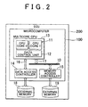
- FIG 2 illustrates an example of a block diagram of the microcomputer that carries a multicore CPU according to the first and second embodiments of the invention.
- FIG. 3 illustrates an example of system layout of an ECU according to the first and second embodiments of the invention.
- the microcomputer 100 has a CPU core 0 and a CPU core 1. (As shown in FIG 2 , in a case where the CPU core 0 and CPU core 1 are not distinguished, this is called a CPU core 11, while one system constituted by the CPU core 0 and CPU core 1 is called a multicore CPU 13).
- An OS 21 that is installed in the microcomputer 100 may switch the CPU core 0 and CPU core 1 individually between SMP (Symmetric Multi-Processing) and AMP (Asymmetric Multiprocessing) processing modes (the SMP processing mode and AMP processing mode will be referred to hereinbelow as "SMP mode” and "AMP mode", respectively).
- SMP Symmetric Multi-Processing
- AMP Asymmetric Multiprocessing
- the processing efficiency is increased where the OS 21 and CPU cores 11 are switched dynamically (temporarily when failure diagnosis is performed) from the SMP mode to a BMP processing mode, instead of operating in a complete BMP process.
- the SMP mode is generally a processing mode in which one OS 21 has the CPU core 0, CPU core 1, and one memory, and the OS 21 dynamically allocates the tasks to the CPU core 11 with a small processing load. Thus, there is no connection between the task and CPU core 11, and from the standpoint of OS 21, the CPU cores are equivalent.
- the AMP mode is generally a processing mode in which the tasks allocated to the CPU core 11 are determined in advance. In this mode, even if the processing load of a certain CPU core 11 is small, the task that is an object of execution may not be executed by the CPU core 11 with a small processing load unless the task that is an object of execution is the task that has been allocated to this CPU core 11.
- the BMP mode is a processing mode in which one OS 21 allocates a specific task to a specific CPU core and other tasks are dynamically allocated to the remaining CPU core.
- the CPU core 0 and CPU core 1 initially execute the standard processing in the SMP mode ("I" in FIG 1 ).
- the standard processing is control or data processing that is requested at all times for the CPU cores 11 based on the operations conducted by the vehicle driver, travel state of the vehicle, or vehicle state, in other words, the processing other than a task of detecting a failure.
- the standard processing is typically constituted by a plurality of different tasks.
- the OS 21 checks that no effect will be produced on the execution speed of standard processing (that the processing load is below the threshold) even when only the CPU core 1 will execute the standard processing, before switching the CPU core 0 from the SMP mode to the AMP mode ("II" in FIG. 1 ).
- the standard processing may be ensured to be executed without delays even when the CPU core 0 is in the AMP mode and executes only a task of failure diagnosis when failure diagnosis is conducted.
- the OS 21 switches the CPU core (in this case, CPU core 0) 11 that is the object of failure diagnosis from the SMP mode to the AMP mode.
- the special task executed by the CPU core 0 in the AMP mode is the failure diagnostic task.
- the CPU core 0 in the AMP mode does not execute any task other than the failure diagnostic task.
- the CPU core 1 remains in the SMP mode, and the CPU core 1 continues the standard processing ("III" in FIG. 1 ).
- the OS 21 switches the CPU core 0 from the AMP mode to the SMP mode ("IV" in FIG 1 ).
- the OS 21 switches the CPU core 1 from the SMP mode to the AMP mode and allocates the failure diagnostic task to the CPU core 1 in a procedure similar to the failure diagnosis of the CPU core 0 shown in FIG 1 .
- a microcomputer 100 has the multicore CPU 13, a data access controller 14, a memory access controller 15, and data buses 16, 17.
- the multicore CPU 13 has a CPU core 0, a CPU core 1, and a data control unit 12.
- the data access controller 14 is connected to an external memory 18, and the memory access controller 15 is connected to the external memory 19.
- the multicore CPU 13 may be installed at an LSI, rather than the microcomputer 100.
- An Electronic Control Unit (ECU) 200 installed at a vehicle may be realized by the microcomputer 100, external memory 18, and external memory 19.
- the processing of displaying a road map on a display device on the basis of position information detected by a global positioning system (GPS) receiver and searching a route to the destination, video processing of television or camera images, and voice processing or radio or CD player are the examples of standard processing.
- the standard processing is a processing of adequately controlling the fuel injection amount, fuel injection timing, opening-closing timing of intake and exhaust valves, throttle opening degree, and ignition timing of an igniter.
- the installation at a body ECU, brake ECU, and various ECU 200 for assisting driving is also possible. In the embodiment, failure diagnosis is conducted without affecting the execution speed of these kinds of standard processing. Therefore, a processing that requires real time execution ability may be also defined as the standard processing.
- the data control unit 12 controls CPU communication between the CPU core 0 and CPU core 1.
- a function of notifying the state of CPU core 11 at each cycle time and a function of transmitting and receiving data between the CPU core 0 and CPU core 1 via a shared memory may be considered as typical functions of CPU communication.
- the data control unit 12 checks the compatibility of processing results. Further, the CPU core 11 may interrupt the CPU core 1 from the CPU core 0 (and conversely) by using the prepared Application Programming Interface (API) and sending a request to the data control unit 12.
- API Application Programming Interface
- the data bus 17 is a bus that is used by the CPU core 11 during standard processing.
- the data bus 16 is a bus that is used by the CPU core 11 during failure diagnosis.
- the data control unit 12 causes the CPU core 11 to access the external memory 18 via the data bus 16.
- the CPU core 1 conducts standard processing even when the CPU core 0 executes a task of failure diagnosis
- by providing separately the data bus 17 that is used during standard processing and the data bus 16 that is used during failure diagnosis it is possible to increase a bus load of the data bus 17 during failure diagnosis and prevent any effect on the execution speed of standard processing.
- the data access controller 14 accesses the external memory 18 in response to a request from the data control unit 12 during failure diagnosis and reads the below-described test data and expected value.
- the external memory 19 is a memory device of a comparatively large capacity (for example, Hard Drive Disk (HDD) or Solid State Disk (SSD)) that stores the application programs, OS 21, and files necessary for the standard processing.
- the data control unit 12 sends an access request of the CPU core 11 that is executing the standard processing to the memory access controller 15 via the data bus 17.
- IP Intellectual Property
- IC Integrated Circuit
- CAN Control Area Network
- motor control circuit a circuit such as a radio tuner, a television tuner, an AV decoder, a sound recognition/synthesizing circuit, a Bluetooth circuit, and a touch panel sensor circuit.
- the IP of an audio system are connected to speakers via an amplifier, and the IP of a video system are connected to a display.
- FIG. 3 shows an example of system layers of the ECU 200.
- FIG 3 shows system layers in which the microcomputer 100 is installed at the ECU 200 of a multimedia system.
- the layer that is the closest to the multicore CPU 13 is a layer of the OS 21.
- the layer of the OS 21 actually includes middleware that provides a device driver and virtual execution environment for controlling an actuator and executes specific computations such as protocol processing or data compression and expansion.
- the OS 21 controls the operation of switching the CPU core 11 from the SMP mode to the AMP mode.
- the layer above the OS 21 is a layer of a User Interface (UI) control application 22 and a functional logic 23.
- the UI control application 22 controls the UI that is displayed on a display by the ECU 200 of a multimedia system.
- the uppermost layer as shown in the figure, is a UI application 29 for various functions that control the UI to make it visible to the user.
- a Human-machine Interface (HMI) application 25 for navigation generates a UI relating to the navigation function or generates a UI of a menu to be operated by the user.
- the HMI application 26 of a video system generates a UI for video such as DVD or television or generates a UI of a menu by which the user operates this function.
- the HMI application 27 of an audio system generates a UI relating to an audio function such as radio or television sound or generates a UI of a menu to be operated by the user.
- the vehicle-related HMI application 28 for example, generates a UI for the user to operate the functions relating to vehicle control that uses position information or a UI for displaying the alarm signals or messages.
- the UI control application 22 may control the display of UI generated by the UI application 29 of each function. For example, the control may be performed such that only the UI of a predetermined function is displayed over the entire screen of the display, or all the UI are divided and displayed on the display, or only the UI of a predetermined function is not displayed.
- the operated UI application 29 calls out the API corresponding to the operation with respect to the HMI-API 24, and the HMI-API 24 calls out the predetermined functional logic 23 according to the called-out API.
- the functional logic 23 is a navigation logic 23a, a video system logic 23b, an audio system logic 23c, and a vehicle-related logic 23d.
- the logic is used for each function of the ECU 200. Where the UI application 29 for each function and functional logic 23 are thus separated, the degree of freedom in development is increased. For example, it is possible to change only the UI, while leaving the functional logic 23 as is.
- the data control unit 12 will be described below with reference to FIG. 4 .
- the data control unit 12 has three multiplexers (MUX) 41, 42, and 45, a mode control unit 43, a CPU number register 44, and a comparison block 46.
- the CPU core 0 is connected to the MUX 41, and the CPU core 1 is connected to the MUX 42.
- the MUX 41 is connected to both the data access controller 14 and the memory access controller 15.
- the MUX 42 is also connected to both the data access controller 14 and the memory access controller 15.
- the mode control unit 43 is connected to the MUX 41, MUX 42, CPU core 0, and CPU core 1.
- the MUX 45 is connected to the CPU core 0 and CPU core 1.
- the MUX 45 is also connected to the comparison block 46.
- the mode control unit 43 switches the processing modes of the CPU core 0 and CPU core 1.
- the mode control unit 43 switches the CPU core 0 to the AMP mode, while leaving the CPU core 1 in the SMP mode, and switches the CPU core 1 into the AMP mode, while leaving the CPU core 0 in the SMP mode.
- a "High" signal is inputted in the CPU core 11 that is to be switched to the AMP mode.
- the internal switch of the CPU core 11 that has been switched to the AMP mode is switched ON/OFF to form a connection line or a logic circuit designated for failure diagnosis.
- the logic circuit for failure diagnosis may complete the failure diagnosis within a short time, for example, by making it possible to obtain the processing results of failure diagnosis in several blocks.
- the CPU core 0 that has been switched to the AMP mode outputs the processing results to the MUX 45
- the CPU core 1 that has been switched to the AMP mode outputs the processing results to the MUX 45.
- the processing results only from the CPU core 11 in the AMP mode are inputted in the MUX 45.
- the mode control unit 43 also switches the processing modes of the MUX 41 and 42.
- the MUX 41 and 42 output an access request to the memory access controller 15 in the SMP mode and output an access request to the data access controller 14 in the AMP mode.
- the mode control unit 43 switches the MUX 41 to the AMP mode and leaves the MUX 42 in the SMP mode. More specifically, the mode control unit 43 inputs, for example, a "High" signal to the MUX 41.
- the mode control unit 43 switches the MUX 42 to the AMP mode and leaves the MUX 41 in the SMP mode. More specifically, the mode control unit 43 inputs, for example, a "High" signal to the MUX 42.
- the MUX 45 inputs the processing results inputted from the CPU core 11 in the AMP mode in the comparison block 46.
- the comparison block 46 has a processing result storage unit 46a that stores the processing results, a comparator 46b, and an expected value storage unit 46c.
- the processing result storage unit 46a stores the processing results.
- the expected value storage unit 46c stores the expected value 38 of the processing result, that is, the correct processing result.
- the expected value 38 is stored in advance in the external memory 18, and where the OS 21 switches either of the CPU cores 11 to the AMP mode, the OS 21 reads the expected value from the external memory 18 to the expected value storage unit 46c.
- the processing result storage unit 46a and expected value storage unit 46c are constituted, for example, by a dynamic random access memory (DRAM) or a register, and are not necessary physically separated.
- the comparator 46b compares the processing result of the processing result storage unit 46a with the expected value 38 of the expected value storage unit 46c and determines whether the results match. For example, when the results match, a "High" signal is outputted. It is also possible to determine whether either of the processing result and expected value 38 is below a predetermined threshold. The determination result is a failure diagnostic result.
- a CPU number register 44 is a register that stores an identification number of the CPU core.
- the mode control unit 43 stores in the CPU number register 44 the identification number of the CPU core 11 that is next to be subjected to failure diagnosis.
- the mode control unit 43 increments the CPU number register 44 each time the failure diagnosis of one CPU core 11 is completed. Further, where the "NUMBER - 1" of the CPU cores 11 installed in the multicore CPU 13 is reached, the storage contents of the CPU number register 44 returns to "0". As a result, a plurality of CPU cores may be uniformly subjected to failure diagnosis, instead of conducting failure diagnosis of the same CPU core 11.
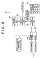
- FIG. 5 shows an example of a functional block provided by the OS 21.
- FIGS. 6A and 6B show examples of explanatory drawings illustrating schematically the load prediction.
- the OS 21 (for example, a scheduler) allocates the tasks A to C to the CPU cores 11, while referring to the processing load of the CPU cores 11.
- the tasks B, A are registered in a task cue 31 of the CPU core 0, and the tasks A to C are registered in a task cue 32 of the CPU core 1. Therefore, the future processing load may be predicted by referring to the task cues 31, 32.
- the load prediction unit 34 stores a table 33 in which the tasks are associated with Million Instructions PerSecond (MIPS)) values.
- MIPS Million Instructions PerSecond
- the task A is a program that issues 1,000,000 instructions per 1 sec, and has a processing load higher than that of other tasks B and C.
- the processing load of the CPU core 11 tends to be higher with the task with a high MIPS value.
- the load prediction unit 34 reads the task that is being executed in the CPU core 11 and the tasks of the task cues 31, 32, reads the MIPS value from the table 33, and predicts the processing load of the multicore CPU 13.
- FIG. 6A shows an example illustrating the prediction of temporal changes in the processing load of the CPU core 11.
- the application has already been known in advance and, therefore, the MIPS value may be specified for each task of the application.
- a time in future to which a load is to be predicted is a time necessary to execute at least the task of failure diagnosis.
- the task of failure diagnosis corresponds to the test data 37 or to the execution of the test data 37. This is because the CPU core 11 that has executed the task of failure diagnosis returns to standard processing, without any effect being produced on the execution speed of standard processing, unless the processing load of the multicore CPU 13 exceeds the processing load of the CPU core 11 before the execution of the task of failure diagnosis is completed.
- the longest period is about 1 sec, and taking into account the overhead such as switching from the SMP mode to the AMP mode and reading of test data 37 and the like, the period may be assumed to be completed within less than 1 sec to several seconds.
- FIG. 6A With consideration for the completion time of each task, where the processing loads of CPU cores 11 overlap, it is possible to obtain FIG. 6B that predicts the processing load of the multicore CPU 13.
- a typical OS 21 such a processing load is stationary monitored and a processing is executed such that allocates the tasks preferentially to the CPU core 11 with empty task cues 31, 32. Therefore, it is preferred that the prediction of load produce no effect of standard processing.
- the prediction of load may be assumed as an additional processing for the multicore CPU 13, because such a prediction of processing load may be performed by specifying a task from the tasks that are being executed and task cues 31, 32 and matching the MIPS value, the prediction of processing load does not become a load that affects the standard processing.
- the load prediction unit 34 determines whether the processing load of the period exceeds the processing capacity of the CPU core 11 (here, the CPU core 1) that continuously executes the standard processing in the SMP mode. Because the processing capacity of the CPU cores 11 is already known and may be also represented by a MIPS value, the comparison may be easily made.
- the processing load of a period A is determined to exceed the processing load of the CPU core 1, but the processing load of a period B is determined not to exceed the processing load of the CPU core 1. Therefore, the task of failure diagnosis of the CPU core 0 is executed from a point of time t2 in which the period A ends (referred to hereinbelow as "time when failure diagnosis may be started").
- the processing capacity of the CPU cores 11 that is compared with the predicted processing load is a sum total of processing capacities of all the remaining CPU cores 11 that do not undergo failure diagnosis. Therefore, for example, in a case where the number of CPU cores 11 is four, the sum total of processing capacities of three CPU cores 11 is an object of comparison with the predicted processing load.
- the failure diagnosis is supposed to be conducted after all these tasks have been executed.
- the period is assumed to start at a time at which the tasks of the CPU cores 11 that are the object of failure diagnosis are completed. Therefore, the processing load that has to be predicted also becomes the processing load of the period.
- the time at which the final task A of the task cue 31 is completed in the CPU core 0 becomes the start point of the period, as shown in FIG. 6A . More specifically, it is possible that the failure diagnosis may be started each time the "period" elapses since the start point.
- the load prediction unit 34 predicts a processing load of the task C and subsequent tasks executed by other CPU core 1 from the time the task A is completed (task C is shown in FIG. 6B , but the task that is executed by the CPU core 1 when the CPU core 0 ends the task A changes depending on the execution time of each task by the CPU core 1).
- the load prediction unit 34 may find a period in which the processing load of the multicore CPU 13 does not exceed the processing capacity and may allocate again the task that has been allocated to the CPU core 0 to the CPU core 1 that is not the object of failure diagnosis within this period.
- the load prediction unit 34 finds a period in which the failure diagnosis is possible, the load prediction unit notifies the mode switching unit 35 about the time at which the failure diagnosis may be started. Where the time at which the failure diagnosis may be started is reached, the mode switching unit 35 (actually, the CPU core 11) outputs a control signal to the mode control unit 43 of the data control unit 12. As a result, as described hereinabove, the data control unit 12 switches the processing modes of the CPU core 11 and MUX 41, 42 in order to execute the task of failure diagnosis.
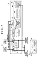
- FIGS. 7 to 10 illustrate one example in which the operations of the data control unit 12 when the CPU core 11 is switched to the AMP mode.
- FIG. 7 shows the data control unit 12 immediately after the mode switching unit 35 has outputted a control signal to the mode control unit 43.
- the mode control unit 43 refers to the CPU number register 44 and detects "0"
- the mode control unit switches the CPU core 0 and MUX 41 to the AMP mode.
- the MUX 41 may access the data access controller 14, and the CPU core 0 may access the MUX 45.
- FIG. 8 illustrates a flow of data when the CPU core 0 reads out the test data 37 of failure diagnosis and expected value 38.
- the CPU core 0 that has been switched to the AMP mode requests the data access controller 14 to read the test data 37 and expected value 38 from the external memory 18 via the MUX 41.
- the CPU core 0 cashes the test data 37 and sets the address of the test data 37 into the register.
- the data access controller 14 directly reads Direct Memory Access (DMA) the expected value 38 from the external memory 18 into the comparison block 46.
- DMA Direct Memory Access
- the test data 37 may be appropriate data that may be inputted into the microcomputer 100 so as to enable the failure diagnostic unit 36 to use for failure diagnosis the instructions identical to those of the standard processing.
- any test data 37 may be used. It is preferred that the test data 37 be limited to minimum necessary data, because the time necessary for the failure diagnosis (the aforementioned "period") may be minimized.
- the test data 37 including instructions may be also used for the failure diagnosis.
- the test data 37 in this case are instructions (opcodes) and minimum necessary parameters (operands) for determining whether the CPU core 11 is normal. Simple instructions and parameters processed by an operational circuit for expanded function or Arithmetic and Logical Unit (ALU) of the CPU core 11 are used.
- ALU Arithmetic and Logical Unit
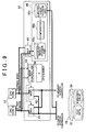
- FIG. 9 illustrates a flow of data after the CPU core 0 has executed the test data 37 of failure diagnosis.
- the CPU core 0 outputs the processing result to the MUX 45.
- the MUX 45 stores the processing result in the processing result storage unit of the comparison block 46.
- the expected value 38 and processing result may be inputted in the comparator 46b, and the comparator 46b compares the two and holds the comparison result or outputs it to the data access controller 14.
- the data access controller 14 stores the comparison result in the external memory 18.
- the comparison result obtained in comparing the expected value 38 and processing result may be outputted to the external memory 18 only when the processing result differs from the expected value. In this case, the execution time of the failure diagnostic task may be shortened.
- the CPU core 1 executes the standard processing during the failure diagnosis, but because the data control unit 12 accesses the external memory 19 or IP via the data bus 17, the increase in bus load caused by the failure diagnosis does not affect the execution speed of standard processing.
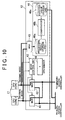
- FIG. 10 shows the data control unit 12 at the time the failure diagnosis is completed.
- the mode control unit 43 increments the value of the CPU number register 44 immediately after the processing mode of the CPU core 0 has been switched. Therefore, the value of the CPU number register 44 becomes "1". As a result, the CPU core 1 executes the task (test data 37) of the next failure diagnosis.
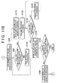
- FIG 11 A and FIG. 11B shows an example of a flowchart illustrating a procedure of failure diagnosis conducted by the microcomputer 100 with respect to each CPU core.
- the CPU core 0 is considered as an object of failure diagnosis.
- Failure diagnosis is not required to be executed that frequently. For example, even if a failure may occur due to degradation with time, it is suffice to conduct failure diagnosis with a frequency of about once a day.
- the OS 21 stores day-time information relating to the very last failure diagnosis.
- the procedure shown in FIG 11A and FIG. 11B is started, for example, when a time equal to or longer than a failure diagnostic time interval (for example, one day) elapses since the very last failure diagnosis, with reference to the day-time information, for each ignition ON.
- a failure diagnostic time interval for example, one day
- the failure diagnosis may be conducted with at least a one-day interval when the vehicle is operated.
- the day-time information is stored in association with the CPU core in the external memory 18, and a diagnostic interval may be set for each CPU core.
- the OS 21 reads the day-time information and failure diagnostic time interval from the external memory 18 (S10) and compares the time that has elapsed before the present point in time and the failure diagnostic time interval (S20). In a case where the elapsed time exceeds the failure diagnostic time interval (Yes in S20), the load prediction unit 34 is caused to predict the processing load (S30).
- the load prediction unit 34 specifies the CPU core 0 that is the object of failure diagnosis from the value of the CPU number register 44.
- the load prediction unit 34 predicts the end time of the very last task allocated to the task cue 31 of the CPU core 0 and predicts the processing load of each period from the end time (S30).
- the mode switching unit 35 does not switch the CPU core 0 to the AMP mode.
- the OS 21 disperses the load between all the CPU cores 0 and CPU cores 1 in the SMP mode (S50) and continues standard processing (S60).
- the load prediction unit 34 waits for the passage of the period in which the processing load has been predicted (S70), and once the period elapses, returns to step S30 and again predicts the load.
- the mode switching unit 35 specifies the CPU core 0 that is the object of failure diagnosis from the value of the CPU number register 44 (S80).
- the mode switching unit 35 receives the time at which the failure diagnosis may be started from the load prediction unit 34.
- the mode switching unit 35 waits till when the failure diagnosis may be started (S90).
- the CPU core 0 that is the object of failure diagnosis executes the task that has been allocated to the task cue 31 still in the SMP mode till when the failure diagnosis may be started (S100).
- the processing load may be predicted again immediately before the time at which the failure diagnosis may be started.
- the mode switching unit 35 requests that the data control unit 12 switch the processing mode of the CPU core 0 (S110).
- the mode control unit 43 of the data control unit 12 switches the CPU core 0 from the SMP mode to the AMP mode and switches the processing mode of the MUX 41 from the SMP mode to the AMP mode.
- the CPU core 0 that has been switched to the AMP mode starts failure diagnosis (S120). As described above, the CPU core 0 reads the test data 37 from the external memory 18 and realizes the failure diagnostic unit 36, and the data access controller 14 reads the expected value from the external memory 18 to the expected value storage unit 46c.
- the failure diagnostic unit 36 determines whether the diagnosis has been completed (S130). Whether the diagnosis has been completed may be determined, for example, based on whether the diagnosis has been executed before the very end of test data 37 or whether the comparator 46b has outputted the comparison result. In a case where the failure diagnosis has not been completed (No in S130), the failure diagnostic unit 36 continues executing the test data 37 in the AMP mode (S140).
- the failure diagnostic unit 36 requests the mode switching unit 35 to switch the processing mode.
- the mode switching unit 35 requests the data control unit 12 to switching the processing mode of the CPU core 0, and the mode control unit 43 of the data control unit 12 switches the CPU core 0 from the AMP mode to the SMP mode and switches the processing mode of the MUX 41 from the AMP mode to the SMP mode (S 150).
- the mode control unit 43 increments the value of the CPU number register 44 (S160), when the CPU core whose diagnosis has not been completed is present (S155). As a result, the number of CPU core that is next to be subjected to failure diagnosis is set to "1" in the CPU number register 44.
- failure diagnosis of one CPU core 0 is thus completed. Therefore, the processing flow returns to step S30, and the OS 21 executes failure diagnosis of the CPU core 1. Failure diagnosis of all the CPU cores 11 may be executed, for example, for each ignition ON by repeating the above-described procedure the number of times equal to the number of CPU cores in the multicore CPU 13.
- the multicore CPU 13 disconnects this CPU core 11 from the multicore CPU 13 and the standard processing may be executed only by the remaining CPU cores 11.
- the standard processing may be continued after the processing results of standard processing have been ensured.
- FIG. 12 shows an example of a block diagram of the microcomputer 100 having installed therein the multicore CPU 13 having four CPU cores 0 to 3.
- the components identical to those shown in FIG. 2 are assigned with same reference numerals and explanation thereof is omitted.
- the failure diagnosis of the embodiment may be applied to any multicore CPU 13, regardless of the number of CPU cores 11.
- the CPU number register 44 of the data control unit 12 is used in a 2-bit configuration to make it suitable for the four CPU cores 11. Furthermore, a total of four MUX are provided at the data access controller 14 side of the data control unit 12, and each MUX is connected to the respective CPU cores 0 to 3. The MUX 45 and CPU cores 0 to 3 are respectively connected.
- the mode control unit 43 switches one of the CPU cores 0 to 3 and one (which corresponds to the one of the CPU cores 0 to 3) of the four MUX alternatively from the SMP mode to the AMP mode, thereby enabling the OS 21 to execute failure diagnosis of each CPU core 11.
- the procedure of failure diagnosis is similar to that shown in FIG. 11A and FIG. 11B , and steps S10 to S160 may be repeated the number of times equal to the number of CPU cores 11. If it is possible to perform failure diagnosis of a plurality of CPU cores concurrently without affecting the execution speed of standard processing, failure diagnosis of a plurality of CPU cores may be performed concurrently.
- FIG 13 shows an example of a block-diagram of the microcomputer 100 of the fourth embodiment in which the external memory 18 is provided in the data control unit 12.
- the test data 37 may be the same, regardless of the passage of time, and where the test data 37 are not changed, the expected value also may be the same.
- the external memory may thus be incorporated in the data control unit 12. In this case, it is not necessary for the data access controller 14 to read the test data 37 and expected values from the external memory 18, and the failure diagnostic time may be shortened.
- the external memory 18 incorporated in the data control unit 12 is in the form of Read Only Memory (ROM), Random Access Memory (RAM), electrically erasable programmable memory (EEPROM), or the like.
- ROM Read Only Memory
- RAM Random Access Memory
- EEPROM electrically erasable programmable memory
- data are, for example, read from the external memory 19 and stored in the RAM when the microcomputer 100 is started.
- the microcomputer 100 of the embodiment may perform failure diagnosis individually for each CPU core 11 of the multicore CPU 13, without affecting the standard processing, by switching the CPU core 11 that is the object of failure diagnosis from the SMP mode to the AMP mode only when the standard processing may be executed without obstacles by the CPU cores 11 that are not the objects of failure diagnosis.
Abstract
Description
- The invention relates to a failure diagnostic system for a multicore central processing unit (CPU) that is provided with a plurality of CPU cores, and more particularly to a failure diagnostic system that performs a failure diagnosis of each CPU core individually, an electronic control unit (ECU) for a vehicle, and a failure diagnostic method.
- Mutual abnormality detection is sometimes conducted by detecting abnormality in a LSI or microcomputer by using a configuration in which a plurality of LSI or microcomputers are installed in one system and monitoring a watchdog signal transmitted from one large scale integration (LSI) (microcomputer) to another LSI (microcomputer). Further, in a multicore processor in which one microcomputer carries a plurality of CPU cores, an abnormality is detected by executing the same processing in a plurality of CPU and comparing the processing results. Further, Japanese Patent Application Publication No.
7-230392 JP-A-7-230392 -
FIG 14 is a block-diagram of a processor that conducts self-diagnosis according toJP-A-7-230392 code comparison unit 4. The code comparison unit compares the two instruction intrinsic codes and detects a failure in the processor if the codes differ from each other. - However, executing the same processing in a plurality of CPU or executing a certain instruction for abnormality detection, as shown in
FIG. 14 , may put pressure upon resources of the microcomputer or processor, thereby affecting the execution speed of standard processing (reducing the execution speed of standard processing with respect to the usual one) such as control or data processing that is essentially required for the processor. - A conventional multicore processor has a processing mode that is Symmetric Multi-Processing (or called as SMP), a processing mode that is Asymmetric Multiprocessing (or called as AMP), and a processing mode that is Bound Multiprocessing (or called as BMP) combining the SMP and AMP. Further, for example, Japanese Patent Application Publication No.
2008-123439 JP-A-2008-123439 JP-A-2008-123439 - However, the OS disclosed in the
JP-A-2008-123439 JP-A-7-230392
US 2008/091974 discloses a failure diagnostic system for a multicore CPU having installed therein a plurality of CPU cores. The system performs diagnoses of the CPU cores in asymmetric multiprocessing mode. In case a CPU core is diagnosed with a failure, a CPU core in symmetric multiprocessing mode is switched to asymmetric multiprocessing mode in order to take over the work of the failing CPU core. - The invention as defined in the appended independent claims provides a failure diagnostic system that may specify a CPU core in which an abnormality has occurred from among a plurality of CPU cores, without affecting the execution speed of standard processing, and also an ECU for a vehicle and a failure diagnostic method.
- The first aspect of the invention relates to a failure diagnostic system for a multicore CPU having installed therein a plurality of CPU cores that is configured to be switched from a SMP mode to an AMP mode, the system including: load prediction means for predicting a processing load of the multicore CPU; mode switching means for switching at least one of the CPU cores to the AMP mode when the processing load is less than a threshold; and failure diagnostic means for performing failure diagnosis of the CPU core that has been switched to the AMP mode.
- In the failure diagnostic system according to the first aspect, the load prediction means may predict a processing load of the multicore CPU in a period required for the failure diagnostic means to conduct failure diagnosis.
- Further, in the failure diagnostic system according to the first aspect, the load prediction means may establish the period that is started at a point of time in which a task executed by the CPU core to be switched to the AMP mode ends.
- Further, the failure diagnostic system according to the first aspect may further include a first data bus dedicated to the CPU core in the SMP mode; a second data bus dedicated to the CPU core in the AMP mode; and data control means for connecting the CPU core in the SMP mode to the first data bus and connecting the CPU core in the AMP mode to the second data bus.
- Further, in the failure diagnostic system according to the first aspect, the data control means may have a plurality of multiplexor units connected to a plurality of the CPU cores respectively; and the mode switching means may switch a connection destination of the multiplexor unit connected to the CPU core that has been switched to the AMP mode from the first data bus to the second data bus.
- Further, in the failure diagnostic system according to the first aspect, the failure diagnostic means compares a processing results of test data for failure diagnosis with an expected value that has been stored in advance, and conduct failure diagnosis of the CPU core that has been switched to the AMP mode based on whether the processing results and the expected value are in conformity.
- Further, the failure diagnostic system according to the first aspect may further include an external memory that stores the test data and the expected value, wherein the failure diagnostic means may read the test data and the expected value via the second data bus.
- Further, in the failure diagnostic system according to the first aspect, a result of the comparison between the processing result of the test data and the expected value may be stored in the external memory.
- Further, in the failure diagnostic system according to the first aspect, the data control means may store the test data and the expected value.
- Further, in the failure diagnostic system according to the first aspect, when the failure diagnostic means detects a failure of the CPU core, the CPU core may be disconnected from the multicore CPU and tasks are distributed only to the remaining CPU cores that have not been diagnosed as having failed..
- Further, in the failure diagnostic system according to the first aspect, the threshold of a processing load may be set to a value such that the processing capacity of standard processing in the CPU core in the SMP mode does not decrease when the CPU core switched to the AMP mode undergoes failure diagnosis.
- Further, in the failure diagnostic system according to the first aspect, the standard processing may be a processing that requires real time execution ability.
- Further, the failure diagnostic system according to the first aspect may further include storage means for storing as information a time at which failure diagnosis has been performed, wherein the failure diagnosis may be conducted again in a case where a time elapsed since the last failure diagnosis exceeds a predetermined time.
- An ECU for a vehicle according to the second aspect of the invention includes the failure diagnostic system according to the first aspect; navigation means; video output means; and audio output means.
- The third aspect of the invention relates to a failure diagnostic method for a multicore CPU having installed therein a plurality of CPU cores that is configured to be switched from a SMP mode to an AMP mode, the method including: predicting a processing load of the multicore CPU; switching at least one of the CPU cores to the AMP mode when the processing load is less than a threshold; and performing failure diagnosis of the CPU core that has been switched to the AMP mode.
- The invention may provide a failure diagnostic system that may specify a CPU core in which an abnormality has occurred from among a plurality of CPU cores, without affecting the execution speed of standard processing, and also an ECU for a vehicle and a failure diagnostic method.
- The foregoing and/or further objects, features and advantages of the invention will become more apparent from the following description of example embodiments with reference to the accompanying drawings, in which like numerals are used to represent like elements, and wherein:
-
FIG. 1 is an example drawing illustrating schematically failure diagnosis of a microcomputer according to the first embodiment of the invention; -
FIG. 2 illustrates an example of a block diagram of the microcomputer that carries a multicore CPU according to the first and second embodiments of the invention; -
FIG. 3 illustrates an example of system layers of an ECU according to the first and second embodiments of the invention; -
FIG 4 illustrates an example of a configuration diagram of the data control unit according to the second embodiment of the invention; -
FIG 5 is illustrates an example of a functional block provided by the OS according to the second embodiment of the invention; -
FIGS. 6A and 6B illustrate schematically an example of the load prediction according to the second embodiment of the invention; -
FIG. 7 shows a data control unit immediately after the mode switching unit according to the second embodiment of the invention has outputted a control signal to the mode control unit; -
FIG 8 explains a flow of data when theCPU core 0 according to the second embodiment of the invention reads the test data of failure diagnosis and expected value; -
FIG. 9 illustrates a flow of data after theCPU core 0 according to the second embodiment of the invention has executed the test data of failure diagnosis; -
FIG. 10 shows a data control unit at completion of diagnostic processing according to the second embodiment of the invention; -
FIG. 11A andFIG 11B is an example of a flowchart illustrating the procedure in which the microcomputer according to the second embodiment of the invention conducts failure diagnosis for each CPU core; -
FIG. 12 shows an example of a block-diagram of the microcomputer having installed therein a multicore CPU having fourCPU cores 0 to 3 according to the third embodiment of the invention; -
FIG 13 is an example of a block-diagram of the microcomputer in which an external memory is provided in the data control unit according to the fourth embodiment of the invention; and -
FIG. 14 is a block diagram of a processor that performs self-diagnosis according to the related art. - Embodiments of the invention will be explained below with reference to the appended drawings.
- A first embodiment will initially be explained.
FIG 1 is an example drawing illustrating schematically failure diagnosis of amicrocomputer 100 according to the first embodiment of the invention.FIG 2 illustrates an example of a block diagram of the microcomputer that carries a multicore CPU according to the first and second embodiments of the invention.FIG. 3 illustrates an example of system layout of an ECU according to the first and second embodiments of the invention. Themicrocomputer 100 has aCPU core 0 and aCPU core 1. (As shown inFIG 2 , in a case where theCPU core 0 andCPU core 1 are not distinguished, this is called aCPU core 11, while one system constituted by theCPU core 0 andCPU core 1 is called a multicore CPU 13). AnOS 21 that is installed in themicrocomputer 100 may switch theCPU core 0 andCPU core 1 individually between SMP (Symmetric Multi-Processing) and AMP (Asymmetric Multiprocessing) processing modes (the SMP processing mode and AMP processing mode will be referred to hereinbelow as "SMP mode" and "AMP mode", respectively). Thus, the processing efficiency is increased where theOS 21 andCPU cores 11 are switched dynamically (temporarily when failure diagnosis is performed) from the SMP mode to a BMP processing mode, instead of operating in a complete BMP process. - The SMP mode is generally a processing mode in which one
OS 21 has theCPU core 0,CPU core 1, and one memory, and theOS 21 dynamically allocates the tasks to theCPU core 11 with a small processing load. Thus, there is no connection between the task andCPU core 11, and from the standpoint ofOS 21, the CPU cores are equivalent. The AMP mode is generally a processing mode in which the tasks allocated to theCPU core 11 are determined in advance. In this mode, even if the processing load of acertain CPU core 11 is small, the task that is an object of execution may not be executed by theCPU core 11 with a small processing load unless the task that is an object of execution is the task that has been allocated to thisCPU core 11. Further, the BMP mode is a processing mode in which oneOS 21 allocates a specific task to a specific CPU core and other tasks are dynamically allocated to the remaining CPU core. - Referring to
FIG. 1 , theCPU core 0 andCPU core 1 initially execute the standard processing in the SMP mode ("I" inFIG 1 ). The standard processing is control or data processing that is requested at all times for theCPU cores 11 based on the operations conducted by the vehicle driver, travel state of the vehicle, or vehicle state, in other words, the processing other than a task of detecting a failure. The standard processing is typically constituted by a plurality of different tasks. - At a timing of failure diagnosis of the
CPU core 0, theOS 21 checks that no effect will be produced on the execution speed of standard processing (that the processing load is below the threshold) even when only theCPU core 1 will execute the standard processing, before switching theCPU core 0 from the SMP mode to the AMP mode ("II" inFIG. 1 ). As a result, the standard processing may be ensured to be executed without delays even when theCPU core 0 is in the AMP mode and executes only a task of failure diagnosis when failure diagnosis is conducted. - The
OS 21 switches the CPU core (in this case, CPU core 0) 11 that is the object of failure diagnosis from the SMP mode to the AMP mode. The special task executed by theCPU core 0 in the AMP mode is the failure diagnostic task. TheCPU core 0 in the AMP mode does not execute any task other than the failure diagnostic task. By contrast, theCPU core 1 remains in the SMP mode, and theCPU core 1 continues the standard processing ("III" inFIG. 1 ). - Once the
CPU core 0 completes the failure diagnostic task, theOS 21 switches theCPU core 0 from the AMP mode to the SMP mode ("IV" inFIG 1 ). - Further, at a timing of failure diagnosis of the
CPU core 1, theOS 21 switches theCPU core 1 from the SMP mode to the AMP mode and allocates the failure diagnostic task to theCPU core 1 in a procedure similar to the failure diagnosis of theCPU core 0 shown inFIG 1 . - By installing a
multicore CPU 13 andOS 21 that may be switched between the SMP mode and AMP mode and checking before the switching as to whether the processing load is such that the standard processing may be conducted without delays by oneCPU core 11, it is possible to conduct individual failure diagnosis of eachCPU core 11 of themulticore CPU 13, without affecting the execution speed of standard processing. - The second embodiment will be explained below. In
FIG. 2 , amicrocomputer 100 has themulticore CPU 13, adata access controller 14, amemory access controller 15, anddata buses multicore CPU 13 has aCPU core 0, aCPU core 1, and adata control unit 12. Thedata access controller 14 is connected to anexternal memory 18, and thememory access controller 15 is connected to theexternal memory 19. Themulticore CPU 13 may be installed at an LSI, rather than themicrocomputer 100. - An Electronic Control Unit (ECU) 200 installed at a vehicle may be realized by the
microcomputer 100,external memory 18, andexternal memory 19. For example, in theECU 200 of a multimedia system, the processing of displaying a road map on a display device on the basis of position information detected by a global positioning system (GPS) receiver and searching a route to the destination, video processing of television or camera images, and voice processing or radio or CD player are the examples of standard processing. In the engine ECU, the standard processing is a processing of adequately controlling the fuel injection amount, fuel injection timing, opening-closing timing of intake and exhaust valves, throttle opening degree, and ignition timing of an igniter. Further, the installation at a body ECU, brake ECU, andvarious ECU 200 for assisting driving is also possible. In the embodiment, failure diagnosis is conducted without affecting the execution speed of these kinds of standard processing. Therefore, a processing that requires real time execution ability may be also defined as the standard processing. - The data control
unit 12 controls CPU communication between theCPU core 0 andCPU core 1. A function of notifying the state ofCPU core 11 at each cycle time and a function of transmitting and receiving data between theCPU core 0 andCPU core 1 via a shared memory may be considered as typical functions of CPU communication. For example, in a case where the twoCPU cores 11 execute the same application and use the mutually obtained processing results, thedata control unit 12 checks the compatibility of processing results. Further, theCPU core 11 may interrupt theCPU core 1 from the CPU core 0 (and conversely) by using the prepared Application Programming Interface (API) and sending a request to thedata control unit 12. - The
data bus 17 is a bus that is used by theCPU core 11 during standard processing. Thedata bus 16 is a bus that is used by theCPU core 11 during failure diagnosis. At a failure diagnostic timing, thedata control unit 12 causes theCPU core 11 to access theexternal memory 18 via thedata bus 16. For example, because theCPU core 1 conducts standard processing even when theCPU core 0 executes a task of failure diagnosis, by providing separately thedata bus 17 that is used during standard processing and thedata bus 16 that is used during failure diagnosis, it is possible to increase a bus load of thedata bus 17 during failure diagnosis and prevent any effect on the execution speed of standard processing. - The
data access controller 14 accesses theexternal memory 18 in response to a request from thedata control unit 12 during failure diagnosis and reads the below-described test data and expected value. - The
external memory 19 is a memory device of a comparatively large capacity (for example, Hard Drive Disk (HDD) or Solid State Disk (SSD)) that stores the application programs,OS 21, and files necessary for the standard processing. The data controlunit 12 sends an access request of theCPU core 11 that is executing the standard processing to thememory access controller 15 via thedata bus 17. - Various kinds of Intellectual Property (IP) (not shown in the figure) are connected to the
bus 10. These IP are an Integrated Circuit (IC) such as a power circuit, an I/O interface circuit, a Control Area Network (CAN) communication circuit, and a motor control circuit. In a case where themicrocomputer 100 is installed at theECU 200 of a multimedia system, IC such as a radio tuner, a television tuner, an AV decoder, a sound recognition/synthesizing circuit, a Bluetooth circuit, and a touch panel sensor circuit are the IP. The IP of an audio system are connected to speakers via an amplifier, and the IP of a video system are connected to a display. -
FIG. 3 shows an example of system layers of theECU 200. Thus,FIG 3 shows system layers in which themicrocomputer 100 is installed at theECU 200 of a multimedia system. The layer that is the closest to themulticore CPU 13 is a layer of theOS 21. The layer of theOS 21 actually includes middleware that provides a device driver and virtual execution environment for controlling an actuator and executes specific computations such as protocol processing or data compression and expansion. In the embodiment, theOS 21 controls the operation of switching theCPU core 11 from the SMP mode to the AMP mode. - The layer above the
OS 21 is a layer of a User Interface (UI)control application 22 and afunctional logic 23. TheUI control application 22 controls the UI that is displayed on a display by theECU 200 of a multimedia system. The uppermost layer, as shown in the figure, is aUI application 29 for various functions that control the UI to make it visible to the user. A Human-machine Interface (HMI)application 25 for navigation generates a UI relating to the navigation function or generates a UI of a menu to be operated by the user. TheHMI application 26 of a video system generates a UI for video such as DVD or television or generates a UI of a menu by which the user operates this function. TheHMI application 27 of an audio system generates a UI relating to an audio function such as radio or television sound or generates a UI of a menu to be operated by the user. The vehicle-relatedHMI application 28, for example, generates a UI for the user to operate the functions relating to vehicle control that uses position information or a UI for displaying the alarm signals or messages. - The
UI control application 22 may control the display of UI generated by theUI application 29 of each function. For example, the control may be performed such that only the UI of a predetermined function is displayed over the entire screen of the display, or all the UI are divided and displayed on the display, or only the UI of a predetermined function is not displayed. - An HMI-
API 24, which is a layer located between theUI control application 22 andUI application 29 for each function, represents the API for theUI application 29 of each function to call out afunctional logic 23. For example, where the user inputs an operation with respect to apredetermined UI application 29, the operatedUI application 29 calls out the API corresponding to the operation with respect to the HMI-API 24, and the HMI-API 24 calls out the predeterminedfunctional logic 23 according to the called-out API. - The
functional logic 23 is anavigation logic 23a, avideo system logic 23b, anaudio system logic 23c, and a vehicle-relatedlogic 23d. The logic is used for each function of theECU 200. Where theUI application 29 for each function andfunctional logic 23 are thus separated, the degree of freedom in development is increased. For example, it is possible to change only the UI, while leaving thefunctional logic 23 as is. - The data control
unit 12 will be described below with reference toFIG. 4 . The data controlunit 12 has three multiplexers (MUX) 41, 42, and 45, amode control unit 43, aCPU number register 44, and acomparison block 46. TheCPU core 0 is connected to theMUX 41, and theCPU core 1 is connected to theMUX 42. TheMUX 41 is connected to both thedata access controller 14 and thememory access controller 15. TheMUX 42 is also connected to both thedata access controller 14 and thememory access controller 15. Themode control unit 43 is connected to theMUX 41,MUX 42,CPU core 0, andCPU core 1. TheMUX 45 is connected to theCPU core 0 andCPU core 1. TheMUX 45 is also connected to thecomparison block 46. - The
mode control unit 43 switches the processing modes of theCPU core 0 andCPU core 1. Thus, themode control unit 43 switches theCPU core 0 to the AMP mode, while leaving theCPU core 1 in the SMP mode, and switches theCPU core 1 into the AMP mode, while leaving theCPU core 0 in the SMP mode. More specifically, for example, a "High" signal is inputted in theCPU core 11 that is to be switched to the AMP mode. In this case, the internal switch of theCPU core 11 that has been switched to the AMP mode is switched ON/OFF to form a connection line or a logic circuit designated for failure diagnosis. The logic circuit for failure diagnosis may complete the failure diagnosis within a short time, for example, by making it possible to obtain the processing results of failure diagnosis in several blocks. - Further, the
CPU core 0 that has been switched to the AMP mode outputs the processing results to theMUX 45, and theCPU core 1 that has been switched to the AMP mode outputs the processing results to theMUX 45. Thus, the processing results only from theCPU core 11 in the AMP mode are inputted in theMUX 45. - The
mode control unit 43 also switches the processing modes of theMUX MUX memory access controller 15 in the SMP mode and output an access request to thedata access controller 14 in the AMP mode. As a result, in a case where theCPU core 0 is switched to the AMP mode, themode control unit 43 switches theMUX 41 to the AMP mode and leaves theMUX 42 in the SMP mode. More specifically, themode control unit 43 inputs, for example, a "High" signal to theMUX 41. Likewise, in a case where theCPU core 1 is switched to the AMP mode, themode control unit 43 switches theMUX 42 to the AMP mode and leaves theMUX 41 in the SMP mode. More specifically, themode control unit 43 inputs, for example, a "High" signal to theMUX 42. - The
MUX 45 inputs the processing results inputted from theCPU core 11 in the AMP mode in thecomparison block 46. Thecomparison block 46 has a processingresult storage unit 46a that stores the processing results, acomparator 46b, and an expectedvalue storage unit 46c. The processingresult storage unit 46a stores the processing results. The expectedvalue storage unit 46c stores the expectedvalue 38 of the processing result, that is, the correct processing result. The expectedvalue 38 is stored in advance in theexternal memory 18, and where theOS 21 switches either of theCPU cores 11 to the AMP mode, theOS 21 reads the expected value from theexternal memory 18 to the expectedvalue storage unit 46c. The processingresult storage unit 46a and expectedvalue storage unit 46c are constituted, for example, by a dynamic random access memory (DRAM) or a register, and are not necessary physically separated. Thecomparator 46b compares the processing result of the processingresult storage unit 46a with the expectedvalue 38 of the expectedvalue storage unit 46c and determines whether the results match. For example, when the results match, a "High" signal is outputted. It is also possible to determine whether either of the processing result and expectedvalue 38 is below a predetermined threshold. The determination result is a failure diagnostic result. - A
CPU number register 44 is a register that stores an identification number of the CPU core. For example, themode control unit 43 stores in the CPU number register 44 the identification number of theCPU core 11 that is next to be subjected to failure diagnosis. Themode control unit 43 increments the CPU number register 44 each time the failure diagnosis of oneCPU core 11 is completed. Further, where the "NUMBER - 1" of theCPU cores 11 installed in themulticore CPU 13 is reached, the storage contents of the CPU number register 44 returns to "0". As a result, a plurality of CPU cores may be uniformly subjected to failure diagnosis, instead of conducting failure diagnosis of thesame CPU core 11. -
FIG. 5 shows an example of a functional block provided by theOS 21.FIGS. 6A and 6B show examples of explanatory drawings illustrating schematically the load prediction. The OS 21 (for example, a scheduler) allocates the tasks A to C to theCPU cores 11, while referring to the processing load of theCPU cores 11. InFIG. 5 , the tasks B, A are registered in atask cue 31 of theCPU core 0, and the tasks A to C are registered in atask cue 32 of theCPU core 1. Therefore, the future processing load may be predicted by referring to thetask cues - The
load prediction unit 34 stores a table 33 in which the tasks are associated with Million Instructions PerSecond (MIPS)) values. For example, the task A is a program that issues 1,000,000 instructions per 1 sec, and has a processing load higher than that of other tasks B and C. The processing load of theCPU core 11 tends to be higher with the task with a high MIPS value. Theload prediction unit 34 reads the task that is being executed in theCPU core 11 and the tasks of thetask cues multicore CPU 13.FIG. 6A shows an example illustrating the prediction of temporal changes in the processing load of theCPU core 11. In a combination-type system, the application has already been known in advance and, therefore, the MIPS value may be specified for each task of the application. - A time in future to which a load is to be predicted (an interval from the present time at which the load is predicted to the future time will be referred to hereinbelow as "a period") is a time necessary to execute at least the task of failure diagnosis. The task of failure diagnosis corresponds to the
test data 37 or to the execution of thetest data 37. This is because theCPU core 11 that has executed the task of failure diagnosis returns to standard processing, without any effect being produced on the execution speed of standard processing, unless the processing load of themulticore CPU 13 exceeds the processing load of theCPU core 11 before the execution of the task of failure diagnosis is completed. The longest period is about 1 sec, and taking into account the overhead such as switching from the SMP mode to the AMP mode and reading oftest data 37 and the like, the period may be assumed to be completed within less than 1 sec to several seconds. - As shown in
FIG. 6A , with consideration for the completion time of each task, where the processing loads ofCPU cores 11 overlap, it is possible to obtainFIG. 6B that predicts the processing load of themulticore CPU 13. With atypical OS 21, such a processing load is stationary monitored and a processing is executed such that allocates the tasks preferentially to theCPU core 11 withempty task cues multicore CPU 13, because such a prediction of processing load may be performed by specifying a task from the tasks that are being executed andtask cues - As shown in
FIG. 6B , where the relationship between the processing load of themulticore CPU 13 and time is obtained, theload prediction unit 34 determines whether the processing load of the period exceeds the processing capacity of the CPU core 11 (here, the CPU core 1) that continuously executes the standard processing in the SMP mode. Because the processing capacity of theCPU cores 11 is already known and may be also represented by a MIPS value, the comparison may be easily made. - As shown in
FIG 6B , the processing load of a period A is determined to exceed the processing load of theCPU core 1, but the processing load of a period B is determined not to exceed the processing load of theCPU core 1. Therefore, the task of failure diagnosis of theCPU core 0 is executed from a point of time t2 in which the period A ends (referred to hereinbelow as "time when failure diagnosis may be started"). The processing capacity of theCPU cores 11 that is compared with the predicted processing load is a sum total of processing capacities of all the remainingCPU cores 11 that do not undergo failure diagnosis. Therefore, for example, in a case where the number ofCPU cores 11 is four, the sum total of processing capacities of threeCPU cores 11 is an object of comparison with the predicted processing load. - However, in a case where tasks are present that have already been allocated to the
task cues CPU cores 11 that are the object of failure diagnosis are completed. Therefore, the processing load that has to be predicted also becomes the processing load of the period. Thus, in a case where theCPU core 0 undergoes failure diagnosis, the time at which the final task A of thetask cue 31 is completed in theCPU core 0 becomes the start point of the period, as shown inFIG. 6A . More specifically, it is possible that the failure diagnosis may be started each time the "period" elapses since the start point. Theload prediction unit 34 predicts a processing load of the task C and subsequent tasks executed byother CPU core 1 from the time the task A is completed (task C is shown inFIG. 6B , but the task that is executed by theCPU core 1 when theCPU core 0 ends the task A changes depending on the execution time of each task by the CPU core 1). - Where the task that has once been allocated to the
task cue 31 may be allocated again, theload prediction unit 34 may find a period in which the processing load of themulticore CPU 13 does not exceed the processing capacity and may allocate again the task that has been allocated to theCPU core 0 to theCPU core 1 that is not the object of failure diagnosis within this period. - Where the
load prediction unit 34 finds a period in which the failure diagnosis is possible, the load prediction unit notifies themode switching unit 35 about the time at which the failure diagnosis may be started. Where the time at which the failure diagnosis may be started is reached, the mode switching unit 35 (actually, the CPU core 11) outputs a control signal to themode control unit 43 of thedata control unit 12. As a result, as described hereinabove, thedata control unit 12 switches the processing modes of theCPU core 11 andMUX - The
CPU core 11 switched to the AMP mode by themode control unit 43 executes the task of failure diagnosis. Thus, theCPU core 11 realizes the failurediagnostic unit 36 by executing the task of failure diagnosis.FIGS. 7 to 10 illustrate one example in which the operations of thedata control unit 12 when theCPU core 11 is switched to the AMP mode. -
FIG. 7 shows thedata control unit 12 immediately after themode switching unit 35 has outputted a control signal to themode control unit 43. InFIG. 7 , components identical to those shown inFIG. 4 are assigned with same reference numerals and explanation thereof is omitted. Where themode control unit 43 refers to theCPU number register 44 and detects "0", the mode control unit switches theCPU core 0 andMUX 41 to the AMP mode. As a result, theMUX 41 may access thedata access controller 14, and theCPU core 0 may access theMUX 45. -
FIG. 8 illustrates a flow of data when theCPU core 0 reads out thetest data 37 of failure diagnosis and expectedvalue 38. TheCPU core 0 that has been switched to the AMP mode requests thedata access controller 14 to read thetest data 37 and expectedvalue 38 from theexternal memory 18 via theMUX 41. As a result, theCPU core 0 cashes thetest data 37 and sets the address of thetest data 37 into the register. Further, thedata access controller 14 directly reads Direct Memory Access (DMA) the expectedvalue 38 from theexternal memory 18 into thecomparison block 46. - The
test data 37 may be appropriate data that may be inputted into themicrocomputer 100 so as to enable the failurediagnostic unit 36 to use for failure diagnosis the instructions identical to those of the standard processing. Thus, where the expectedvalue 38 that is the processing result obtained when thetest data 37 are executed in thenormal CPU core 11 is known, anytest data 37 may be used. It is preferred that thetest data 37 be limited to minimum necessary data, because the time necessary for the failure diagnosis (the aforementioned "period") may be minimized. - The
test data 37 including instructions may be also used for the failure diagnosis. Thetest data 37 in this case are instructions (opcodes) and minimum necessary parameters (operands) for determining whether theCPU core 11 is normal. Simple instructions and parameters processed by an operational circuit for expanded function or Arithmetic and Logical Unit (ALU) of theCPU core 11 are used. -
FIG. 9 illustrates a flow of data after theCPU core 0 has executed thetest data 37 of failure diagnosis. Where thetest data 37 are executed, theCPU core 0 outputs the processing result to theMUX 45. TheMUX 45 stores the processing result in the processing result storage unit of thecomparison block 46. In this case, the expectedvalue 38 and processing result may be inputted in thecomparator 46b, and thecomparator 46b compares the two and holds the comparison result or outputs it to thedata access controller 14. Thedata access controller 14 stores the comparison result in theexternal memory 18. The comparison result obtained in comparing the expectedvalue 38 and processing result may be outputted to theexternal memory 18 only when the processing result differs from the expected value. In this case, the execution time of the failure diagnostic task may be shortened. - The
CPU core 1 executes the standard processing during the failure diagnosis, but because thedata control unit 12 accesses theexternal memory 19 or IP via thedata bus 17, the increase in bus load caused by the failure diagnosis does not affect the execution speed of standard processing. -
FIG. 10 shows thedata control unit 12 at the time the failure diagnosis is completed. Themode control unit 43 increments the value of the CPU number register 44 immediately after the processing mode of theCPU core 0 has been switched. Therefore, the value of theCPU number register 44 becomes "1". As a result, theCPU core 1 executes the task (test data 37) of the next failure diagnosis. -
FIG 11 A andFIG. 11B shows an example of a flowchart illustrating a procedure of failure diagnosis conducted by themicrocomputer 100 with respect to each CPU core. InFIG 11A andFIG 11B , theCPU core 0 is considered as an object of failure diagnosis. - Failure diagnosis is not required to be executed that frequently. For example, even if a failure may occur due to degradation with time, it is suffice to conduct failure diagnosis with a frequency of about once a day. For this purpose, the
OS 21 stores day-time information relating to the very last failure diagnosis. The procedure shown inFIG 11A andFIG. 11B is started, for example, when a time equal to or longer than a failure diagnostic time interval (for example, one day) elapses since the very last failure diagnosis, with reference to the day-time information, for each ignition ON. When the one day is taken as the failure diagnostic time interval, the failure diagnosis may be conducted with at least a one-day interval when the vehicle is operated. The day-time information is stored in association with the CPU core in theexternal memory 18, and a diagnostic interval may be set for each CPU core. - Where the ignition is switched ON and the
OS 21 is actuated, theOS 21 reads the day-time information and failure diagnostic time interval from the external memory 18 (S10) and compares the time that has elapsed before the present point in time and the failure diagnostic time interval (S20). In a case where the elapsed time exceeds the failure diagnostic time interval (Yes in S20), theload prediction unit 34 is caused to predict the processing load (S30). - The
load prediction unit 34 specifies theCPU core 0 that is the object of failure diagnosis from the value of theCPU number register 44. Theload prediction unit 34 predicts the end time of the very last task allocated to thetask cue 31 of theCPU core 0 and predicts the processing load of each period from the end time (S30). - Whether the processing load exceeds the processing capacity of the
CPU core 1 is then determined for each period (S40). - In a case where the processing capacity of the
CPU core 1 exceeds the processing load (No in S40), the execution speed of standard processing may be affected. Therefore, themode switching unit 35 does not switch theCPU core 0 to the AMP mode. As a result, theOS 21 disperses the load between all theCPU cores 0 andCPU cores 1 in the SMP mode (S50) and continues standard processing (S60). - The
load prediction unit 34 waits for the passage of the period in which the processing load has been predicted (S70), and once the period elapses, returns to step S30 and again predicts the load. - In a case where the processing capacity of one
CPU core 1 is greater than the processing load in step S40 (Yes in S40), themode switching unit 35 specifies theCPU core 0 that is the object of failure diagnosis from the value of the CPU number register 44 (S80). Themode switching unit 35 receives the time at which the failure diagnosis may be started from theload prediction unit 34. - The
mode switching unit 35 waits till when the failure diagnosis may be started (S90). TheCPU core 0 that is the object of failure diagnosis executes the task that has been allocated to thetask cue 31 still in the SMP mode till when the failure diagnosis may be started (S100). The processing load may be predicted again immediately before the time at which the failure diagnosis may be started. - When the time comes at which the failure diagnosis may be started, the
mode switching unit 35 requests that thedata control unit 12 switch the processing mode of the CPU core 0 (S110). As a result, themode control unit 43 of thedata control unit 12 switches theCPU core 0 from the SMP mode to the AMP mode and switches the processing mode of theMUX 41 from the SMP mode to the AMP mode. - In this case, the
CPU core 0 that has been switched to the AMP mode starts failure diagnosis (S120). As described above, theCPU core 0 reads thetest data 37 from theexternal memory 18 and realizes the failurediagnostic unit 36, and thedata access controller 14 reads the expected value from theexternal memory 18 to the expectedvalue storage unit 46c. - The failure
diagnostic unit 36 determines whether the diagnosis has been completed (S130). Whether the diagnosis has been completed may be determined, for example, based on whether the diagnosis has been executed before the very end oftest data 37 or whether thecomparator 46b has outputted the comparison result. In a case where the failure diagnosis has not been completed (No in S130), the failurediagnostic unit 36 continues executing thetest data 37 in the AMP mode (S140). - In a case where the failure diagnosis is completed (Yes in S130), the failure
diagnostic unit 36 requests themode switching unit 35 to switch the processing mode. As a result, themode switching unit 35 requests thedata control unit 12 to switching the processing mode of theCPU core 0, and themode control unit 43 of thedata control unit 12 switches theCPU core 0 from the AMP mode to the SMP mode and switches the processing mode of theMUX 41 from the AMP mode to the SMP mode (S 150). - Further, the
mode control unit 43 increments the value of the CPU number register 44 (S160), when the CPU core whose diagnosis has not been completed is present (S155). As a result, the number of CPU core that is next to be subjected to failure diagnosis is set to "1" in theCPU number register 44. - The failure diagnosis of one
CPU core 0 is thus completed. Therefore, the processing flow returns to step S30, and theOS 21 executes failure diagnosis of theCPU core 1. Failure diagnosis of all theCPU cores 11 may be executed, for example, for each ignition ON by repeating the above-described procedure the number of times equal to the number of CPU cores in themulticore CPU 13. - In a case where a failure of the
CPU core 11 is detected, themulticore CPU 13 disconnects thisCPU core 11 from themulticore CPU 13 and the standard processing may be executed only by the remainingCPU cores 11. In this case, although the processing capacity has decreased, the standard processing may be continued after the processing results of standard processing have been ensured. In this process, it is preferred that an important task with a high priority order be established and that only the established task, from among the standard processing tasks, be executed. A failsafe mode of themicrocomputer 100 is thus possible and protection of the microcomputer from failure is increased. - The
microcomputer 100 that uses the failure diagnosis explained in the first and second embodiments will be explained below as the third embodiment.FIG. 12 shows an example of a block diagram of themicrocomputer 100 having installed therein themulticore CPU 13 having fourCPU cores 0 to 3. InFIG. 12 , the components identical to those shown inFIG. 2 are assigned with same reference numerals and explanation thereof is omitted. - Where one of two
CPU cores other CPU core 11. Therefore, the period in which the predicted processing load does not exceed the processing capacity of oneCPU core 11 may be shortened, and in this case a time necessary for failure diagnosis sometimes may not be selected (by contrast, in a case where four CPU cores are present, the period in which the processing capacity is not exceeded is comparatively long, and therefore failure diagnosis is mostly possible). By contrast, even if oneCPU core 11 from among the fourCPU cores 0 to 3 undergoes failure diagnosis, theOS 21 disperses the load, while the threeCPU cores 11 are still in the SMP mode. Therefore, the period may be easily detected. Thus, the failure diagnosis of the embodiment may be applied to anymulticore CPU 13, regardless of the number ofCPU cores 11. - In a case where the
multicore CPU 13 has fourCPU cores 11, as shown inFIG. 12 , the CPU number register 44 of thedata control unit 12 is used in a 2-bit configuration to make it suitable for the fourCPU cores 11. Furthermore, a total of four MUX are provided at thedata access controller 14 side of thedata control unit 12, and each MUX is connected to therespective CPU cores 0 to 3. TheMUX 45 andCPU cores 0 to 3 are respectively connected. Themode control unit 43 switches one of theCPU cores 0 to 3 and one (which corresponds to the one of theCPU cores 0 to 3) of the four MUX alternatively from the SMP mode to the AMP mode, thereby enabling theOS 21 to execute failure diagnosis of eachCPU core 11. - The procedure of failure diagnosis is similar to that shown in
FIG. 11A andFIG. 11B , and steps S10 to S160 may be repeated the number of times equal to the number ofCPU cores 11. If it is possible to perform failure diagnosis of a plurality of CPU cores concurrently without affecting the execution speed of standard processing, failure diagnosis of a plurality of CPU cores may be performed concurrently. - In the configuration shown in
FIG 2 , theexternal memory 18 is externally attached to themicrocomputer 100, but theexternal memory 18 may be also provided inside themicrocomputer 100.FIG 13 shows an example of a block-diagram of themicrocomputer 100 of the fourth embodiment in which theexternal memory 18 is provided in thedata control unit 12. InFIG 13 , the components identical to those shown inFIG 2 are assigned with same reference numerals and explanation thereof is herein omitted. Thetest data 37 may be the same, regardless of the passage of time, and where thetest data 37 are not changed, the expected value also may be the same. - Therefore, the external memory may thus be incorporated in the
data control unit 12. In this case, it is not necessary for thedata access controller 14 to read thetest data 37 and expected values from theexternal memory 18, and the failure diagnostic time may be shortened. Theexternal memory 18 incorporated in thedata control unit 12 is in the form of Read Only Memory (ROM), Random Access Memory (RAM), electrically erasable programmable memory (EEPROM), or the like. In a case where a RAM is incorporated, data are, for example, read from theexternal memory 19 and stored in the RAM when themicrocomputer 100 is started. - As described hereinabove, the
microcomputer 100 of the embodiment may perform failure diagnosis individually for eachCPU core 11 of themulticore CPU 13, without affecting the standard processing, by switching theCPU core 11 that is the object of failure diagnosis from the SMP mode to the AMP mode only when the standard processing may be executed without obstacles by theCPU cores 11 that are not the objects of failure diagnosis. - While the invention has been described with reference to example embodiments thereof, it should be understood that the invention is not limited to the example embodiments or constructions. To the contrary, the invention is intended to cover various modifications and equivalent arrangements. In addition, while the various elements of the example embodiments are shown in various combinations and configurations, which are exemplary, other combinations and configurations, including more, less or only a single element, are also within the scope of the invention.
Claims (15)
- A failure diagnostic system for a multicore CPU (13) having installed therein a plurality of CPU cores (11), said CPU cores (11) being configured to be switched from a symmetric multiprocessing (SMP) mode to an asymmetric multiprocessing (AMP) mode, the system being characterized by comprising:load prediction means (34) for predicting a processing load of the CPU cores (11);mode switching means (35) for switching at least one of the CPU cores (11) to the AMP mode when the processing load is less than a threshold; andfailure diagnostic means (36) for performing failure diagnosis of the CPU core (11) that has been switched to the AMP mode.
- The failure diagnostic system according to claim 1, wherein the load prediction means (34) predicts a processing load of the multicore CPU (13) in a period required for the failure diagnostic means (36) to conduct failure diagnosis.
- The failure diagnostic system according to claim 2, wherein the load prediction means (34) establishes the period that is started at a point of time in which a task executed by the CPU core (11) to be switched to the AMP mode ends.
- The failure diagnostic system according to any of claims 1 to 3, further comprising:a first data bus (17) dedicated to the CPU core (11) in the SMP mode;a second data bus (16) dedicated to the CPU core (11) in the AMP mode; anddata control means (12) for connecting the CPU core (11) in the SMP mode to the first data bus (17) and connecting the CPU core (11) in the AMP mode to the second data bus (16).
- The failure diagnostic system according to claim 4, whereinthe data control means (12) has a plurality of multiplexor units connected to a plurality of the CPU cores (11) respectively; andthe mode switching means (35) switches a connection destination of the multiplexor unit connected to the CPU core (11) that has been switched to the AMP mode from the first data bus (17) to the second data bus (16).
- The failure diagnostic system according to claim 4, wherein the failure diagnostic means (36) compares a processing results of test data (37) for failure diagnosis with an expected value (38) that has been stored in advance, and conduct failure diagnosis of the CPU core (11) that has been switched to the AMP mode based on whether the processing results and the expected value (38) are in conformity.
- The failure diagnostic system according to claim 6, further comprising an external memory (18) that stores the test data (37) and the expected value (38), wherein
the failure diagnostic means (36) reads the test data (37) and the expected value (38) via the second data bus (16). - The failure diagnostic system according to claim 7, wherein a result of the comparison between the processing result of the test data (37) and the expected value (38) is stored in the external memory (18).
- The failure diagnostic system according to claim 6, wherein the data control means (12) stores the test data (37) and the expected value (38).
- The failure diagnostic system according to any of claims 1 to 9. wherein when the failure diagnostic means (36) detects a failure of the CPU core (11), the CPU core (11) is disconnected from the multicore CPU (13) and tasks are distributed only to the remaining CPU cores (11) that have not been diagnosed as having failed.
- The failure diagnostic system according to any of claims 1 to 10, wherein the threshold of a processing load is set to a value such that a processing capacity of standard processing in the CPU core (11) in the SMP mode does not decrease when the CPU core (11) switched to the AMP mode undergoes failure diagnosis.
- The failure diagnostic system according to claim 11, wherein the standard processing is a processing that requires real time execution ability.
- The failure diagnostic system according to any of claims I to 12, further comprising storage means for storing as information a time at which failure diagnosis has been performed, wherein
the failure diagnosis is conducted again in a case where a time elapsed since the last failure diagnosis exceeds a predetermined time. - An electronic control unit for a vehicle, characterized by comprising:the failure diagnostic system according to any of claims I to 13;navigation means (25);video output means (26); andaudio output means (27).
- A failure diagnostic method for a multicore CPU (13) having installed therein a plurality of CPU cores (11), said CPU cores (11) being configured to be switched from a symmetric multiprocessing (SMP) mode to an asymmetric multiprocessing (AMP) mode, the method comprising:predicting a processing load of the CPU cores (11);switching at least one of the CPU cores (11) to the AMP mode when the processing load is less than a threshold; andfailure diagnosing the CPU core (11) that has been switched to the AMP mode.
Applications Claiming Priority (2)
| Application Number | Priority Date | Filing Date | Title |
|---|---|---|---|
| JP2009064975A JP5316128B2 (en) | 2009-03-17 | 2009-03-17 | Fault diagnosis system, electronic control unit, fault diagnosis method |
| PCT/IB2010/000195 WO2010106403A1 (en) | 2009-03-17 | 2010-02-02 | Failure diagnostic system, electronic control unit for vehicle, failure diagnostic method |
Publications (2)
| Publication Number | Publication Date |
|---|---|
| EP2409230A1 EP2409230A1 (en) | 2012-01-25 |
| EP2409230B1 true EP2409230B1 (en) | 2013-01-16 |
Family
ID=42104439
Family Applications (1)
| Application Number | Title | Priority Date | Filing Date |
|---|---|---|---|
| EP10704588A Active EP2409230B1 (en) | 2009-03-17 | 2010-02-02 | Failure diagnostic system, electronic control unit for vehicle, failure diagnostic method |
Country Status (5)
| Country | Link |
|---|---|
| US (1) | US8656216B2 (en) |
| EP (1) | EP2409230B1 (en) |
| JP (1) | JP5316128B2 (en) |
| CN (1) | CN102741818B (en) |
| WO (1) | WO2010106403A1 (en) |
Families Citing this family (26)
| Publication number | Priority date | Publication date | Assignee | Title |
|---|---|---|---|---|
| JP5527270B2 (en) | 2011-04-12 | 2014-06-18 | 株式会社デンソー | In-vehicle electronic control unit |
| US8826074B2 (en) * | 2011-09-30 | 2014-09-02 | Alcatel Lucent | Live module diagnostic testing |
| JP5853691B2 (en) * | 2011-12-28 | 2016-02-09 | アイシン・エィ・ダブリュ株式会社 | Vehicle control apparatus and method |
| JP5861718B2 (en) * | 2012-02-15 | 2016-02-16 | トヨタ自動車株式会社 | Electronic control device for vehicle and data receiving method |
| JP5900061B2 (en) | 2012-03-19 | 2016-04-06 | 富士通株式会社 | Test method, test apparatus and program |
| US9384055B2 (en) * | 2012-04-16 | 2016-07-05 | International Business Machines Corporation | Programmatic load-based management of processor population |
| CN104798046A (en) * | 2012-10-01 | 2015-07-22 | Abb技术有限公司 | Symmetric multi-processor arrangement, safety critical system, and method therefor |
| DE102012222215A1 (en) * | 2012-12-04 | 2014-06-05 | Robert Bosch Gmbh | Method for operating a real-time critical application on a control device |
| US9619309B2 (en) * | 2012-12-28 | 2017-04-11 | Intel Corporation | Enforcing different operational configurations for different tasks for failure rate based control of processors |
| KR101457557B1 (en) | 2013-01-18 | 2014-11-04 | 연세대학교 산학협력단 | Multi-core device, test device and method for diagnosing failure |
| KR101944873B1 (en) * | 2013-12-24 | 2019-04-17 | 후아웨이 디바이스 컴퍼니 리미티드 | Method for checking whether hardware of intelligent terminal runs abnormally and intelligent terminal |
| EP3121684B1 (en) * | 2014-07-14 | 2018-05-02 | Huawei Technologies Co., Ltd. | Multi-core processor management method and device |
| CN110290039B (en) * | 2014-09-12 | 2021-08-31 | 松下电器(美国)知识产权公司 | Electronic control unit, in-vehicle network system, and communication method for vehicle |
| US9952650B2 (en) | 2014-10-16 | 2018-04-24 | Futurewei Technologies, Inc. | Hardware apparatus and method for multiple processors dynamic asymmetric and symmetric mode switching |
| US10248180B2 (en) | 2014-10-16 | 2019-04-02 | Futurewei Technologies, Inc. | Fast SMP/ASMP mode-switching hardware apparatus for a low-cost low-power high performance multiple processor system |
| US10928882B2 (en) | 2014-10-16 | 2021-02-23 | Futurewei Technologies, Inc. | Low cost, low power high performance SMP/ASMP multiple-processor system |
| US10234932B2 (en) * | 2015-07-22 | 2019-03-19 | Futurewei Technologies, Inc. | Method and apparatus for a multiple-processor system |
| DE102015216086A1 (en) | 2015-08-24 | 2017-03-02 | Robert Bosch Gmbh | Method and device for monitoring a state of an electronic circuit unit of a vehicle |
| CN105388881B (en) * | 2015-11-04 | 2017-10-20 | 北京长城华冠汽车科技股份有限公司 | The fault detect display device and method of a kind of entire car controller |
| CN105425766B (en) * | 2015-11-04 | 2017-10-20 | 北京长城华冠汽车科技股份有限公司 | The failure detector and method of a kind of entire car controller |
| JP2017102633A (en) * | 2015-12-01 | 2017-06-08 | ルネサスエレクトロニクス株式会社 | Information processing device and semiconductor integrated circuit device |
| US10473711B2 (en) | 2016-04-15 | 2019-11-12 | Infineon Technologies Ag | Multi-channel fault detection with a single diagnosis output |
| JP6867754B2 (en) * | 2016-05-11 | 2021-05-12 | コニカミノルタ株式会社 | Image forming device |
| KR20180028570A (en) * | 2016-09-08 | 2018-03-19 | 현대오트론 주식회사 | Multi core system and method of driving the same |
| US10200875B2 (en) | 2017-04-17 | 2019-02-05 | DeepSig Inc. | Placement and scheduling of radio signal processing dataflow operations |
| CN111891134B (en) * | 2019-05-06 | 2022-09-30 | 北京百度网讯科技有限公司 | Automatic driving processing system, system on chip and method for monitoring processing module |
Family Cites Families (21)
| Publication number | Priority date | Publication date | Assignee | Title |
|---|---|---|---|---|
| JPS62286131A (en) * | 1986-06-05 | 1987-12-12 | Nec Corp | Automatic selfdiagnosing system for information processor |
| JPH04148274A (en) * | 1990-10-08 | 1992-05-21 | Nec Corp | Testing system for information processor |
| JPH06332874A (en) * | 1993-05-24 | 1994-12-02 | Fujitsu Ltd | Test program starting method |
| JP2734940B2 (en) * | 1993-07-26 | 1998-04-02 | 日本電気株式会社 | Semiconductor integrated circuit device |
| JP2990008B2 (en) * | 1994-02-18 | 1999-12-13 | 日本電気通信システム株式会社 | Processor self-diagnosis method |
| US5682491A (en) * | 1994-12-29 | 1997-10-28 | International Business Machines Corporation | Selective processing and routing of results among processors controlled by decoding instructions using mask value derived from instruction tag and processor identifier |
| JPH08329024A (en) * | 1995-05-29 | 1996-12-13 | Mitsubishi Electric Corp | Computer system |
| US7206966B2 (en) * | 2003-10-22 | 2007-04-17 | Hewlett-Packard Development Company, L.P. | Fault-tolerant multi-core microprocessing |
| JP2005190038A (en) * | 2003-12-25 | 2005-07-14 | Hitachi Ltd | Diagnostic processing method and diagnostic processing program for processor |
| US7428663B2 (en) * | 2004-06-01 | 2008-09-23 | Alcatel Lucent | Electronic device diagnostic methods and systems |
| GB0507150D0 (en) * | 2005-04-08 | 2005-05-18 | Ibm | A method or apparatus for running a test program in a computer system |
| US8448162B2 (en) * | 2005-12-28 | 2013-05-21 | Foundry Networks, Llc | Hitless software upgrades |
| JP2007249491A (en) | 2006-03-15 | 2007-09-27 | Fujitsu Ltd | Program, device and method for distributing batch job in multi-server environment |
| US8555288B2 (en) * | 2006-05-17 | 2013-10-08 | Teradata Us, Inc. | Managing database utilities to improve throughput and concurrency |
| JP2007328461A (en) * | 2006-06-06 | 2007-12-20 | Matsushita Electric Ind Co Ltd | Asymmetric multiprocessor |
| JP2008123439A (en) * | 2006-11-15 | 2008-05-29 | Denso Corp | Operating system, program and mobile body manipulation support apparatus |
| JP2008097280A (en) * | 2006-10-11 | 2008-04-24 | Denso Corp | Control apparatus of multicore cpu for mobile object, microcomputer for mobile object and mobile object operation supporting apparatus |
| US20080091974A1 (en) * | 2006-10-11 | 2008-04-17 | Denso Corporation | Device for controlling a multi-core CPU for mobile body, and operating system for the same |
| GB2443277B (en) * | 2006-10-24 | 2011-05-18 | Advanced Risc Mach Ltd | Performing diagnostics operations upon an asymmetric multiprocessor apparatus |
| EP2085882A4 (en) * | 2006-11-02 | 2010-01-27 | Nec Corp | Multiprocessor system, system configuration method in multiprocessor system, and program thereof |
| US20100242014A1 (en) * | 2009-03-17 | 2010-09-23 | Xiaohan Zhu | Symmetric multi-processor operating system for asymmetric multi-processor architecture |
-
2009
- 2009-03-17 JP JP2009064975A patent/JP5316128B2/en active Active
-
2010
- 2010-02-02 US US13/257,121 patent/US8656216B2/en active Active
- 2010-02-02 WO PCT/IB2010/000195 patent/WO2010106403A1/en active Application Filing
- 2010-02-02 CN CN201080012408.0A patent/CN102741818B/en active Active
- 2010-02-02 EP EP10704588A patent/EP2409230B1/en active Active
Also Published As
| Publication number | Publication date |
|---|---|
| JP2010218277A (en) | 2010-09-30 |
| US8656216B2 (en) | 2014-02-18 |
| EP2409230A1 (en) | 2012-01-25 |
| WO2010106403A1 (en) | 2010-09-23 |
| CN102741818B (en) | 2015-01-28 |
| CN102741818A (en) | 2012-10-17 |
| JP5316128B2 (en) | 2013-10-16 |
| US20120005535A1 (en) | 2012-01-05 |
Similar Documents
| Publication | Publication Date | Title |
|---|---|---|
| EP2409230B1 (en) | Failure diagnostic system, electronic control unit for vehicle, failure diagnostic method | |
| JP6189004B1 (en) | Shared backup unit and control system | |
| US8417990B2 (en) | Multi-core processing system for vehicle control or an internal combustion engine controller | |
| JP2010285001A (en) | Electronic control system and functional agency method | |
| JP2008123439A (en) | Operating system, program and mobile body manipulation support apparatus | |
| JP2008305317A (en) | Multiprocessor system and control method thereof | |
| JP2010113388A (en) | Multi-core microcontroller having comparator for collating processing result | |
| WO2011141992A1 (en) | Fault diagnosis device and fault diagnosis method | |
| JP6838222B2 (en) | Vehicle control device and vehicle system | |
| US7558990B2 (en) | Semiconductor circuit device and method of detecting runaway | |
| US7685351B2 (en) | External device access apparatus | |
| JP2007334403A (en) | System and method for supporting trouble of computer system | |
| JP2015067107A (en) | Vehicle control device | |
| US20170154480A1 (en) | Information processing apparatus and large scale integrated circuit | |
| WO2012070137A1 (en) | Processor, electronic control device, creation program | |
| KR20090000008A (en) | Anticollision system among diagnosis terminals and method thereof | |
| US10269194B2 (en) | Multiprocessor system and vehicle control system | |
| JP2007018207A (en) | Data processor, electronic control unit, and automobile | |
| JP5978873B2 (en) | Electronic control unit | |
| JP2010018168A (en) | System and method for analyzing abnormality for vehicle, and vehicular trouble analyzer | |
| TWI816106B (en) | Controller for a user interface of a motor vehicle, and method for operating a controller for a user interface | |
| JP2017204286A (en) | Vehicle control device | |
| CN116476763A (en) | Hierarchical power management system and method for vehicles | |
| JPH10247185A (en) | Fault diagnostic system for processor | |
| CN114879931A (en) | Onboard audio path management method and system supporting multiple operating systems |
Legal Events
| Date | Code | Title | Description |
|---|---|---|---|
| PUAI | Public reference made under article 153(3) epc to a published international application that has entered the european phase |
Free format text: ORIGINAL CODE: 0009012 |
|
| 17P | Request for examination filed |
Effective date: 20110916 |
|
| AK | Designated contracting states |
Kind code of ref document: A1 Designated state(s): AT BE BG CH CY CZ DE DK EE ES FI FR GB GR HR HU IE IS IT LI LT LU LV MC MK MT NL NO PL PT RO SE SI SK SM TR |
|
| DAX | Request for extension of the european patent (deleted) | ||
| GRAP | Despatch of communication of intention to grant a patent |
Free format text: ORIGINAL CODE: EPIDOSNIGR1 |
|
| GRAS | Grant fee paid |
Free format text: ORIGINAL CODE: EPIDOSNIGR3 |
|
| GRAA | (expected) grant |
Free format text: ORIGINAL CODE: 0009210 |
|
| AK | Designated contracting states |
Kind code of ref document: B1 Designated state(s): AT BE BG CH CY CZ DE DK EE ES FI FR GB GR HR HU IE IS IT LI LT LU LV MC MK MT NL NO PL PT RO SE SI SK SM TR |
|
| REG | Reference to a national code |
Ref country code: GB Ref legal event code: FG4D |
|
| REG | Reference to a national code |
Ref country code: CH Ref legal event code: EP |
|
| REG | Reference to a national code |
Ref country code: IE Ref legal event code: FG4D |
|
| REG | Reference to a national code |
Ref country code: AT Ref legal event code: REF Ref document number: 594204 Country of ref document: AT Kind code of ref document: T Effective date: 20130215 Ref country code: CH Ref legal event code: EP |
|
| RAP2 | Party data changed (patent owner data changed or rights of a patent transferred) |
Owner name: TOYOTA JIDOSHA KABUSHIKI KAISHA |
|
| REG | Reference to a national code |
Ref country code: DE Ref legal event code: R096 Ref document number: 602010004679 Country of ref document: DE Effective date: 20130314 |
|
| REG | Reference to a national code |
Ref country code: AT Ref legal event code: MK05 Ref document number: 594204 Country of ref document: AT Kind code of ref document: T Effective date: 20130116 |
|
| REG | Reference to a national code |
Ref country code: NL Ref legal event code: VDEP Effective date: 20130116 |
|
| REG | Reference to a national code |
Ref country code: LT Ref legal event code: MG4D |
|
| PG25 | Lapsed in a contracting state [announced via postgrant information from national office to epo] |
Ref country code: AT Free format text: LAPSE BECAUSE OF FAILURE TO SUBMIT A TRANSLATION OF THE DESCRIPTION OR TO PAY THE FEE WITHIN THE PRESCRIBED TIME-LIMIT Effective date: 20130116 Ref country code: BE Free format text: LAPSE BECAUSE OF FAILURE TO SUBMIT A TRANSLATION OF THE DESCRIPTION OR TO PAY THE FEE WITHIN THE PRESCRIBED TIME-LIMIT Effective date: 20130116 Ref country code: NO Free format text: LAPSE BECAUSE OF FAILURE TO SUBMIT A TRANSLATION OF THE DESCRIPTION OR TO PAY THE FEE WITHIN THE PRESCRIBED TIME-LIMIT Effective date: 20130416 Ref country code: SE Free format text: LAPSE BECAUSE OF FAILURE TO SUBMIT A TRANSLATION OF THE DESCRIPTION OR TO PAY THE FEE WITHIN THE PRESCRIBED TIME-LIMIT Effective date: 20130116 Ref country code: IS Free format text: LAPSE BECAUSE OF FAILURE TO SUBMIT A TRANSLATION OF THE DESCRIPTION OR TO PAY THE FEE WITHIN THE PRESCRIBED TIME-LIMIT Effective date: 20130516 Ref country code: BG Free format text: LAPSE BECAUSE OF FAILURE TO SUBMIT A TRANSLATION OF THE DESCRIPTION OR TO PAY THE FEE WITHIN THE PRESCRIBED TIME-LIMIT Effective date: 20130416 Ref country code: ES Free format text: LAPSE BECAUSE OF FAILURE TO SUBMIT A TRANSLATION OF THE DESCRIPTION OR TO PAY THE FEE WITHIN THE PRESCRIBED TIME-LIMIT Effective date: 20130427 Ref country code: LT Free format text: LAPSE BECAUSE OF FAILURE TO SUBMIT A TRANSLATION OF THE DESCRIPTION OR TO PAY THE FEE WITHIN THE PRESCRIBED TIME-LIMIT Effective date: 20130116 |
|
| PG25 | Lapsed in a contracting state [announced via postgrant information from national office to epo] |
Ref country code: SI Free format text: LAPSE BECAUSE OF FAILURE TO SUBMIT A TRANSLATION OF THE DESCRIPTION OR TO PAY THE FEE WITHIN THE PRESCRIBED TIME-LIMIT Effective date: 20130116 Ref country code: GR Free format text: LAPSE BECAUSE OF FAILURE TO SUBMIT A TRANSLATION OF THE DESCRIPTION OR TO PAY THE FEE WITHIN THE PRESCRIBED TIME-LIMIT Effective date: 20130417 Ref country code: NL Free format text: LAPSE BECAUSE OF FAILURE TO SUBMIT A TRANSLATION OF THE DESCRIPTION OR TO PAY THE FEE WITHIN THE PRESCRIBED TIME-LIMIT Effective date: 20130116 Ref country code: FI Free format text: LAPSE BECAUSE OF FAILURE TO SUBMIT A TRANSLATION OF THE DESCRIPTION OR TO PAY THE FEE WITHIN THE PRESCRIBED TIME-LIMIT Effective date: 20130116 Ref country code: LV Free format text: LAPSE BECAUSE OF FAILURE TO SUBMIT A TRANSLATION OF THE DESCRIPTION OR TO PAY THE FEE WITHIN THE PRESCRIBED TIME-LIMIT Effective date: 20130116 Ref country code: PT Free format text: LAPSE BECAUSE OF FAILURE TO SUBMIT A TRANSLATION OF THE DESCRIPTION OR TO PAY THE FEE WITHIN THE PRESCRIBED TIME-LIMIT Effective date: 20130516 Ref country code: PL Free format text: LAPSE BECAUSE OF FAILURE TO SUBMIT A TRANSLATION OF THE DESCRIPTION OR TO PAY THE FEE WITHIN THE PRESCRIBED TIME-LIMIT Effective date: 20130116 |
|
| PG25 | Lapsed in a contracting state [announced via postgrant information from national office to epo] |
Ref country code: HR Free format text: LAPSE BECAUSE OF FAILURE TO SUBMIT A TRANSLATION OF THE DESCRIPTION OR TO PAY THE FEE WITHIN THE PRESCRIBED TIME-LIMIT Effective date: 20130116 Ref country code: MC Free format text: LAPSE BECAUSE OF NON-PAYMENT OF DUE FEES Effective date: 20130228 |
|
| PG25 | Lapsed in a contracting state [announced via postgrant information from national office to epo] |
Ref country code: SK Free format text: LAPSE BECAUSE OF FAILURE TO SUBMIT A TRANSLATION OF THE DESCRIPTION OR TO PAY THE FEE WITHIN THE PRESCRIBED TIME-LIMIT Effective date: 20130116 Ref country code: RO Free format text: LAPSE BECAUSE OF FAILURE TO SUBMIT A TRANSLATION OF THE DESCRIPTION OR TO PAY THE FEE WITHIN THE PRESCRIBED TIME-LIMIT Effective date: 20130116 Ref country code: EE Free format text: LAPSE BECAUSE OF FAILURE TO SUBMIT A TRANSLATION OF THE DESCRIPTION OR TO PAY THE FEE WITHIN THE PRESCRIBED TIME-LIMIT Effective date: 20130116 Ref country code: DK Free format text: LAPSE BECAUSE OF FAILURE TO SUBMIT A TRANSLATION OF THE DESCRIPTION OR TO PAY THE FEE WITHIN THE PRESCRIBED TIME-LIMIT Effective date: 20130116 Ref country code: CZ Free format text: LAPSE BECAUSE OF FAILURE TO SUBMIT A TRANSLATION OF THE DESCRIPTION OR TO PAY THE FEE WITHIN THE PRESCRIBED TIME-LIMIT Effective date: 20130116 |
|
| PLBE | No opposition filed within time limit |
Free format text: ORIGINAL CODE: 0009261 |
|
| STAA | Information on the status of an ep patent application or granted ep patent |
Free format text: STATUS: NO OPPOSITION FILED WITHIN TIME LIMIT |
|
| PG25 | Lapsed in a contracting state [announced via postgrant information from national office to epo] |
Ref country code: CY Free format text: LAPSE BECAUSE OF FAILURE TO SUBMIT A TRANSLATION OF THE DESCRIPTION OR TO PAY THE FEE WITHIN THE PRESCRIBED TIME-LIMIT Effective date: 20130116 |
|
| REG | Reference to a national code |
Ref country code: IE Ref legal event code: MM4A |
|
| 26N | No opposition filed |
Effective date: 20131017 |
|
| PG25 | Lapsed in a contracting state [announced via postgrant information from national office to epo] |
Ref country code: IT Free format text: LAPSE BECAUSE OF FAILURE TO SUBMIT A TRANSLATION OF THE DESCRIPTION OR TO PAY THE FEE WITHIN THE PRESCRIBED TIME-LIMIT Effective date: 20130116 |
|
| PG25 | Lapsed in a contracting state [announced via postgrant information from national office to epo] |
Ref country code: IE Free format text: LAPSE BECAUSE OF NON-PAYMENT OF DUE FEES Effective date: 20130202 |
|
| REG | Reference to a national code |
Ref country code: DE Ref legal event code: R097 Ref document number: 602010004679 Country of ref document: DE Effective date: 20131017 |
|
| PG25 | Lapsed in a contracting state [announced via postgrant information from national office to epo] |
Ref country code: MT Free format text: LAPSE BECAUSE OF FAILURE TO SUBMIT A TRANSLATION OF THE DESCRIPTION OR TO PAY THE FEE WITHIN THE PRESCRIBED TIME-LIMIT Effective date: 20130116 |
|
| REG | Reference to a national code |
Ref country code: CH Ref legal event code: PL |
|
| PG25 | Lapsed in a contracting state [announced via postgrant information from national office to epo] |
Ref country code: CH Free format text: LAPSE BECAUSE OF NON-PAYMENT OF DUE FEES Effective date: 20140228 Ref country code: LI Free format text: LAPSE BECAUSE OF NON-PAYMENT OF DUE FEES Effective date: 20140228 |
|
| REG | Reference to a national code |
Ref country code: DE Ref legal event code: R084 Ref document number: 602010004679 Country of ref document: DE |
|
| REG | Reference to a national code |
Ref country code: GB Ref legal event code: 746 Effective date: 20141113 |
|
| REG | Reference to a national code |
Ref country code: DE Ref legal event code: R084 Ref document number: 602010004679 Country of ref document: DE Effective date: 20141117 |
|
| PG25 | Lapsed in a contracting state [announced via postgrant information from national office to epo] |
Ref country code: SM Free format text: LAPSE BECAUSE OF FAILURE TO SUBMIT A TRANSLATION OF THE DESCRIPTION OR TO PAY THE FEE WITHIN THE PRESCRIBED TIME-LIMIT Effective date: 20130116 |
|
| PG25 | Lapsed in a contracting state [announced via postgrant information from national office to epo] |
Ref country code: TR Free format text: LAPSE BECAUSE OF FAILURE TO SUBMIT A TRANSLATION OF THE DESCRIPTION OR TO PAY THE FEE WITHIN THE PRESCRIBED TIME-LIMIT Effective date: 20130116 |
|
| PG25 | Lapsed in a contracting state [announced via postgrant information from national office to epo] |
Ref country code: HU Free format text: LAPSE BECAUSE OF FAILURE TO SUBMIT A TRANSLATION OF THE DESCRIPTION OR TO PAY THE FEE WITHIN THE PRESCRIBED TIME-LIMIT; INVALID AB INITIO Effective date: 20100202 Ref country code: MK Free format text: LAPSE BECAUSE OF FAILURE TO SUBMIT A TRANSLATION OF THE DESCRIPTION OR TO PAY THE FEE WITHIN THE PRESCRIBED TIME-LIMIT Effective date: 20130116 Ref country code: LU Free format text: LAPSE BECAUSE OF NON-PAYMENT OF DUE FEES Effective date: 20130202 |
|
| REG | Reference to a national code |
Ref country code: FR Ref legal event code: PLFP Year of fee payment: 7 |
|
| REG | Reference to a national code |
Ref country code: FR Ref legal event code: PLFP Year of fee payment: 8 |
|
| REG | Reference to a national code |
Ref country code: FR Ref legal event code: PLFP Year of fee payment: 9 |
|
| PGFP | Annual fee paid to national office [announced via postgrant information from national office to epo] |
Ref country code: GB Payment date: 20221230 Year of fee payment: 14 |
|
| PGFP | Annual fee paid to national office [announced via postgrant information from national office to epo] |
Ref country code: FR Payment date: 20230110 Year of fee payment: 14 |
|
| PGFP | Annual fee paid to national office [announced via postgrant information from national office to epo] |
Ref country code: DE Payment date: 20221229 Year of fee payment: 14 |
|
| P01 | Opt-out of the competence of the unified patent court (upc) registered |
Effective date: 20230427 |