EP2405562A1 - Bridgeless power factor correction boost-doubler circuit - Google Patents
Bridgeless power factor correction boost-doubler circuit Download PDFInfo
- Publication number
- EP2405562A1 EP2405562A1 EP11172428A EP11172428A EP2405562A1 EP 2405562 A1 EP2405562 A1 EP 2405562A1 EP 11172428 A EP11172428 A EP 11172428A EP 11172428 A EP11172428 A EP 11172428A EP 2405562 A1 EP2405562 A1 EP 2405562A1
- Authority
- EP
- European Patent Office
- Prior art keywords
- voltage
- power factor
- factor correction
- circuit
- correction circuit
- Prior art date
- Legal status (The legal status is an assumption and is not a legal conclusion. Google has not performed a legal analysis and makes no representation as to the accuracy of the status listed.)
- Withdrawn
Links
Images


Classifications
-
- H—ELECTRICITY
- H02—GENERATION; CONVERSION OR DISTRIBUTION OF ELECTRIC POWER
- H02M—APPARATUS FOR CONVERSION BETWEEN AC AND AC, BETWEEN AC AND DC, OR BETWEEN DC AND DC, AND FOR USE WITH MAINS OR SIMILAR POWER SUPPLY SYSTEMS; CONVERSION OF DC OR AC INPUT POWER INTO SURGE OUTPUT POWER; CONTROL OR REGULATION THEREOF
- H02M1/00—Details of apparatus for conversion
- H02M1/42—Circuits or arrangements for compensating for or adjusting power factor in converters or inverters
- H02M1/4208—Arrangements for improving power factor of AC input
- H02M1/4225—Arrangements for improving power factor of AC input using a non-isolated boost converter
-
- H—ELECTRICITY
- H02—GENERATION; CONVERSION OR DISTRIBUTION OF ELECTRIC POWER
- H02M—APPARATUS FOR CONVERSION BETWEEN AC AND AC, BETWEEN AC AND DC, OR BETWEEN DC AND DC, AND FOR USE WITH MAINS OR SIMILAR POWER SUPPLY SYSTEMS; CONVERSION OF DC OR AC INPUT POWER INTO SURGE OUTPUT POWER; CONTROL OR REGULATION THEREOF
- H02M1/00—Details of apparatus for conversion
- H02M1/0067—Converter structures employing plural converter units, other than for parallel operation of the units on a single load
- H02M1/0077—Plural converter units whose outputs are connected in series
-
- H—ELECTRICITY
- H02—GENERATION; CONVERSION OR DISTRIBUTION OF ELECTRIC POWER
- H02M—APPARATUS FOR CONVERSION BETWEEN AC AND AC, BETWEEN AC AND DC, OR BETWEEN DC AND DC, AND FOR USE WITH MAINS OR SIMILAR POWER SUPPLY SYSTEMS; CONVERSION OF DC OR AC INPUT POWER INTO SURGE OUTPUT POWER; CONTROL OR REGULATION THEREOF
- H02M1/00—Details of apparatus for conversion
- H02M1/0083—Converters characterised by their input or output configuration
- H02M1/0085—Partially controlled bridges
-
- Y—GENERAL TAGGING OF NEW TECHNOLOGICAL DEVELOPMENTS; GENERAL TAGGING OF CROSS-SECTIONAL TECHNOLOGIES SPANNING OVER SEVERAL SECTIONS OF THE IPC; TECHNICAL SUBJECTS COVERED BY FORMER USPC CROSS-REFERENCE ART COLLECTIONS [XRACs] AND DIGESTS
- Y02—TECHNOLOGIES OR APPLICATIONS FOR MITIGATION OR ADAPTATION AGAINST CLIMATE CHANGE
- Y02B—CLIMATE CHANGE MITIGATION TECHNOLOGIES RELATED TO BUILDINGS, e.g. HOUSING, HOUSE APPLIANCES OR RELATED END-USER APPLICATIONS
- Y02B70/00—Technologies for an efficient end-user side electric power management and consumption
- Y02B70/10—Technologies improving the efficiency by using switched-mode power supplies [SMPS], i.e. efficient power electronics conversion e.g. power factor correction or reduction of losses in power supplies or efficient standby modes
-
- Y—GENERAL TAGGING OF NEW TECHNOLOGICAL DEVELOPMENTS; GENERAL TAGGING OF CROSS-SECTIONAL TECHNOLOGIES SPANNING OVER SEVERAL SECTIONS OF THE IPC; TECHNICAL SUBJECTS COVERED BY FORMER USPC CROSS-REFERENCE ART COLLECTIONS [XRACs] AND DIGESTS
- Y02—TECHNOLOGIES OR APPLICATIONS FOR MITIGATION OR ADAPTATION AGAINST CLIMATE CHANGE
- Y02P—CLIMATE CHANGE MITIGATION TECHNOLOGIES IN THE PRODUCTION OR PROCESSING OF GOODS
- Y02P80/00—Climate change mitigation technologies for sector-wide applications
- Y02P80/10—Efficient use of energy, e.g. using compressed air or pressurized fluid as energy carrier
Definitions
- the present invention relates to a voltage-dividing power factor correction circuit, a voltage-dividing power factor correction apparatus, and a voltage-dividing power factor correction method.
- PSUs Power Supply Units designed to convert an input alternating current (AC) voltage to a direct current (DC) voltage are used for supplying power to computers such as servers and personal computers.
- a PSU may cause noise and distribution loss because rectifiers and smoothing capacitors provided in the PSU distort the waveform of an input current. Therefore, a Power Factor Correction (PFC) circuit, which improves the power factor of input electric power (electrical current) to prevent noise and reduce distribution loss, is incorporated in PSUs to confirm to the IEC 1000_3_4 standard.
- PFC Power Factor Correction
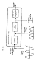
- FIG II illustrates a configuration of a PSU.
- FIG. 12 illustrates a PFC circuit.
- An input AC voltage in the range of 110 V to 240 V, for example, is applied to the PSU illustrated in FIG. 11 .
- a rectifier in the PSU rectifies the applied AC voltage.
- the rectified voltage is applied to the PFC circuit.
- a DC-DC conversion circuit in the PSU converts the DC voltage of 380 V (volts) with a power factor improved by the PFC circuit to a DC voltage of 12 V, which is then supplied to a computer such as a server or a personal computer.
- a computer such as a server or a personal computer.
- a distorted current Iin flows because no PFC circuit is provided.
- a PFC circuit brings the waveform of the current Iin into phase with the waveform of an input voltage Vin to reduce distortion of the current Iin, thereby reducing noise and distribution loss.
- the PFC circuit brings the waveform of an input current closer to a sinusoidal waveform to reduce distortion of the current to improve the power factor of the input electric power. Specifically, when a voltage rectified by the rectifier is applied, the PFC circuit uses high-frequency switching and pulse width modulation to form a current waveform that is closer to the waveform of the input voltage.
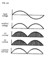
- FIG. 13 3 illustrates a method for improving a power factor.
- FIG. 14 illustrates the effect of the PFC circuit.
- the PFC circuit in the example in FIG. 13 includes a control circuit that drives a field effect transistor (FET) according to an input voltage and an input current.
- FET field effect transistor
- the PFC circuit When a voltage rectified by a bridge diode, which functions as a rectifier, is applied to the PFC circuit, the PFC circuit intermittently turns on the FET to allow current to flow alternately through a path (1) in FIG. 13 and a path (2) in FIG. 13 . As illustrated in FIG. 14 , the PFC circuit then adds the intermittent current flowing through the path (I) and the intermittent current flowing through the path (2) together to bring the waveform of the input current closer to the waveform of the rectified voltage.
- FIG. 15 is a diagram for explaining power loss in the bridge diode.
- High-voltage capacitors and FETs are provided in a PFC circuit because an input voltage increases in the course of correction of the power factor.
- FIG. 16 illustrates resistances of FETs. As illustrated in FIG. 16 , high-voltage FETs have larger current resistances than low-voltage FETs. In addition, high-voltage capacitors and FETs are larger in size than low-voltage capacitors and FETs. Accordingly, a PSU incorporating a PFC circuit has a higher equivalent resistance and a larger footprint than a PSU without a PFC circuit.
- a power factor correction technique using synchronous rectification is known in which a bridge diode is replaced with multiple FETs and a control integrated circuit (IC) in order to avoid the power loss in diodes described above ( US Patent No. 7164591 , National Publication of International Patent Application WO 2007-527687 ).
- a PSU using synchronous rectification in an example illustrated in FIG. 17 7 uses four FETs and a control integrated circuit (IC) to replace a bridge diode in order to reduce power loss.
- An interleaved power factor correction technique is known in which PFC circuits are provided in parallel in order to reduce equivalent series resistance (ESR) caused by the PFC circuits.
- a PSU using interleaved circuitry in an example illustrated in FIG. 18 includes a bridge diode functioning as a rectifier and two PFC circuits provided in parallel.
- Such a PSU applies a voltage rectified by the bridge diode to the two parallel PFC circuits at the same time to reduce ESR in the PFC circuits to half.
- the PSU also reduces ripple current by controlling the parallel PFC circuits so as to operate 180 degrees out of phase with each other.
- the power factor correction technique using synchronous rectification described above has the problem of increase in the footprint of the PSU resulting from the increase in the footprint of the rectifier because the diodes of the bridge diode are replaced with FETs and a control IC for controlling the FETs is added.
- the diodes of the bridge diode are replaced with FETs and a control IC for controlling the FETs is added.
- one bridge diode is replaced with four FETs and a control IC for controlling the FETs is added, resulting in an increased footprint of the rectifier.
- the present invention reduces the footprint of a PSU or reduces power loss in a PSU.
- a voltage-dividing power factor correction circuit includes a first power factor correction circuit that, when a positive AC voltage is applied from an external source, forces current produced by the applied positive AC voltage to be in phase with the applied positive AC voltage so that a power factor of electric power is improved; a second power factor correction circuit that, when a negative AC voltage is applied from an external source, forces current produced by the applied negative AC voltage to be in phase with the applied negative AC voltage so that a power factor of electric power is improved; and an output circuit including a first capacitor storing first electric power with a power factor improved by the first power factor correction circuit and a second capacitor storing second electric power with a power factor improved by the second power factor correction circuit, the first capacitor and the second capacitor being provided in series, the output circuit outputting the first electric power stored in the first capacitor and the second electric power stored in the second capacitor.
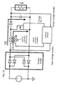
- FIG 1 illustrates a voltage-dividing bridgeless PFC circuit according to the first embodiment.
- the voltage-dividing bridgeless PFC circuit includes at least two power factor correction circuits provided in parallel.
- the voltage-dividing bridgeless PFC circuit 1 includes a first power factor correction circuit 2, a second power factor correction circuit 3, an output circuit 4, and a control circuit 5 and is connected to an external power source 6 and an external resistance R1.
- the external power source 6 is an AC power source which applies an AC voltage to the voltage-dividing bridgeless PFC circuit 1 .
- the first power factor correction circuit 2 forces current produced by the applied positive AC voltage to be in phase with the applied positive AC voltage to improve the power factor of electric power.
- the first power factor correction circuit 2 uses a FET Q1 to force the current produced by the applied positive AC voltage to be in phase with the applied positive AC voltage to improve the power factor of electric power.
- the first power factor correction circuit 2 allows current I1 to flow through itself only when a positive AC voltage is applied from the external power source 6. Accordingly, the first power factor correction circuit 2 forces the current 11 to be in phase with the applied positive AC voltage to improve the power factor of electric power only when the positive AC voltage is applied from the external power source 6. The first power factor correction circuit 2 then stores the electric power with the improve power factor in a capacitor C 1.
- the first power factor correction circuit 2 is connected to the external power source 6 in parallel with the second power factor correction circuit 3, which will be described later. Therefore and because current flows through the first power factor correction circuit 2 only when a positive voltage is applied from the external power source 6, half the AC voltage applied from the external power source 6 is applied to the first power factor correction circuit 2. This means that the first power factor correction circuit 2 may use low-voltage components which are smaller than high-voltage components and therefore may have a smaller footprint than a power factor correction circuit that uses high-voltage components.
- the second power factor correction circuit 3 forces current produced by the applied negative AC voltage to be in phase with the applied negative AC voltage to improve the power factor of electric power.
- the second power factor correction circuit 3 uses a FET Q2 to force current produced by the applied negative AC voltage to be in phase with the applied negative AC voltage to improve the power factor of the electric power.
- the second power factor correction circuit 3 allows current 12 to flow through itself only when a negative AC voltage is applied from the external power source 6. Accordingly, the second power factor correction circuit 3 forces the current 12 to be in phase with the applied negative AC voltage to improve the power factor of electric power only when the negative AC voltage is applied from the external power source 6. The second power factor correction circuit 3 then stores the electric power with the improve power factor in a capacitor C2.
- the second power factor correction circuit 3 is connected to the external power source 6 in parallel with the first power factor correction circuit 2. Therefore and because current flows through the second power factor correction circuit 3 only when a negative voltage is applied from the external power source 6, half the applied voltage from the external power source 6 is applied to the components of the second power factor correction circuit 3. This means that the second power factor correction circuit 3 may use components having half the withstand voltage of conventional ones. Consequently, the footprint of the power factor correction circuit may be reduced compared with a conventional power factor correction circuit.
- the output circuit 4 has the capacitors C1 and C2 connected in series.
- the capacitor C 1 stores electric power with a power factor improved by the first power factor correction circuit 2, whereas the capacitor C2 stores electric power with a power factor improved by the second power factor correction circuit 3.
- the output circuit 4 outputs the electric power stored in the capacitors C 1 and C2 connected in series to the external resistance R1.
- the control circuit 5 detects whether an AC voltage applied from the external power source 6 is positive or negative. When the control circuit 5 detects a positive AC voltage applied from the external power source 6, the control circuit 5 applies a gate voltage to the FET Q1 of the first power factor correction circuit 2; when the control circuit 5 detects a negative AC voltage applied from the external power source 6, the control circuit 5 applies a gate voltage to the FET Q2 of the second power factor correction circuit 3.
- control circuit 5 intermittently turns on the FET Q 1 of the first power factor correction circuit to cause the first power factor correction circuit 2 to improve the power factor of electric power; when a negative voltage is applied from the external power source 6, the control circuit 5 intermittently turns on the FET Q2 of the second power factor correction circuit 3 to cause the second power factor correction circuit 3 to improve the power factor of electric power.
- the voltage-dividing bridgeless PFC circuit 1 includes the first power factor correction circuit 2 that, when a positive AC voltage is applied, forces current produced by the applied positive voltage to be in phase with the applied positive voltage to improve the power factor of electric power.
- the voltage-dividing bridgeless PFC circuit 1 also includes the second power factor correction circuit 3 that is provided in parallel with the first power factor correction circuit 2 and, when a negative AC voltage is applied, forces current produced by the applied negative voltage to be in phase with the applied negative voltage to improve the power factor of electric power.
- the voltage-dividing bridgeless PFC circuit 1 includes a circuit including the first power factor correction circuit 2 that improves the power factor only when a positive AC voltage is applied from the external power source 6 and the second power factor correction circuit 3 that is connected in parallel with the first power factor correction circuit 2 and that improves the power factor only when a negative AC voltage is applied from the external power source 6. Therefore, the voltage-dividing bridgeless PFC circuit 1 may improve the power factor of supplied AC power without using a bridge diode.
- the voltage-dividing bridgeless PFC circuit 1 in the example illustrated in FIG 1 includes the first power factor correction circuit 2 through which current flows when a positive voltage is applied from the external power source 6 and the second power factor correction circuit 3 through which current flows when a negative voltage is applied from the external power source 6.
- the voltage-dividing bridgeless PFC circuit 1 does not need a bridge diode for maintaining the direction of current flowing through the PFC circuit constant and therefore may reduce the number of diodes in a current path to two. That is, the voltage-dividing bridgeless PFC circuit 1 may reduce power loss caused by a bridge diode.
- each of the power factor correction circuits 2 and 3 may reduce a boosted voltage to half compared with a conventional PFC circuit and therefore may use low-voltage components. Consequently, since the voltage-dividing bridgeless PFC circuit 1 may use small, low-voltage components, the footprint of the voltage-dividing bridgeless PFC circuit 1, and therefore the footprint of the PSU, may be reduced.
- the voltage-dividing bridgeless PFC circuit 1 may add voltages output from the power factor correction circuits 2 and 3 together. That is, the voltage-dividing bridgeless PFC circuit 1 reduces a boosted voltage in each of the power factor correction circuit 2 and 3 to half compared with a conventional PFC circuit and yet may maintain an output voltage equivalent to that of the conventional PFC circuit.
- the first power factor correction circuit 2 includes a diode D1, an inductor (coil) L1, a field effect transistor (FET) Q1, a diode D3, and a capacitor C1.
- the first power factor correction circuit 2 has a closed circuit through which current flows from the external power source 6 to the diode D1 to the inductor L1 and to the FET Q1 when a positive AC voltage is applied from the external power source 6.
- the first power factor correction circuit 2 has a closed circuit through which current flows from the external power source 6 to the diode D1 to the inductor L1 to the diode D3 to the capacitor C1 when a positive AC voltage is applied from the external power source 6.
- the FET Q1 is a field effect transistor that forces current to flow from the inductor L1 toward the external power source 6 when a gate voltage Vgs1 is applied from the control circuit 5, which will be described later, to the FET Q1.
- the FET Q1 does not allow current to flow from the inductor L 1 toward the external power source 6 when the gate voltage Vgs 1 is not applied.
- the diode D1 is a diode that allows current to flow from the external power source 6 toward the inductor L1.
- the inductor L1 is a passive element designed to have a specific amount of inductance.
- the diode D3 is a diode that allows current to flow from the inductor L1 toward the capacitor C1.
- the capacitor C 1 is a capacitor that stores electric power having an improved power factor.
- the second power factor correction circuit 3 includes a diode D2, an inductor L2, a FET Q2, a diode D4 and a capacitor C2.
- the second power factor correction circuit 3 has a closed circuit through which current flows from the FET Q2 to the inductor L2 to the diode D2 when a negative AC voltage is applied from the external power source 6.
- the second power factor correction circuit 3 has a closed circuit through which current flows from the external power source 6 to the capacitor C2 to the diode D4 to the inductor L2 to the diode D2 when a negative AC voltage is applied from the external power source 6.
- the FET Q2 is a field effect transistor that allows current to flow from the external power source 6 toward the inductor L2 when a gate voltage Vgs2 is applied from the control circuit 5, which will be described later, to the FET Q2.
- the FET Q2 does not allow current to flow from the external power source 6 toward the inductor L2 when the gate voltage Vgs2 is not applied.
- the diode D2 is a diode that allows current to flow from the inductor L2 toward the external power source 6.
- the inductor L2 is an inductor similar to the inductor L1.
- the diode D4 is a diode that allows current to flow from the capacitor C2 toward the inductor L2.
- the capacitor C2 is a capacitor that stores electric power having an improved power factor.
- the capacitor C2 is connected to the external resistance R1 in series with the capacitor C 1.
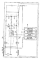
- the control circuit 5 will be described in detail with reference to FIG. 2 , which is a diagram illustrating the control circuit 5.
- the control circuit 5 in the example illustrated in FIG. 2 includes an AC input polarity determination circuit 7, and pulse width modulation (PWM) control circuits 8 and 9.
- the AC input polarity determination circuit 7 includes comparators 10 and 11.
- the PWM control circuit 8 includes an ON/OFF switch 12, an input voltage monitor circuit 13, a current monitor circuit 14, a FET drive signal output circuit 15, and an output voltage monitor circuit 16.
- the PWM control circuit 9 includes an ON/OFF switch 17, an input voltage monitor circuit 18, a current monitor circuit 19, a FET drive signal output circuit 20, and an output voltage monitor circuit 21.
- the AC input polarity determination circuit 7 detects the polarity of an AC voltage applied from the external power source 6. When the AC input polarity determination circuit 7 detects a positive AC voltage, the AC input polarity determination circuit 7 applies a predetermined voltage to the PWM control circuit 8; when the AC input polarity determination circuit 7 detects a negative AC voltage, the AC input polarity determination circuit 7 applies a predetermined voltage to the PWM control circuit 9.
- the PWM control circuit 8 measures the value of input voltage applied from the external power source 6 to the first power factor correction circuit 2. The PWM control circuit 8 also measures the value of current flowing in the inductor L1. The PWM control circuit 8 measures the value of output voltage between the capacitor C1 and the external resistance R1.
- the PWM control circuit 8 When a voltage is applied from the AC input polarity determination circuit 7 to the PWM control circuit 8, the PWM control circuit 8 intermittently applies the gate voltage Vgs1 to the FET Q1 according to the measured input voltage value, current value and output voltage value.
- the PWM control circuit 9 measures the value of input voltage applied from the external power source 6 to the second power factor correction circuit 3.
- the PWM control circuit 9 measures the value of current flowing in the inductor L2.
- the PWM control circuit 9 also measures the value of output voltage between the capacitor C1 and the external resistance R1.
- the PWM control circuit 9 When a voltage is applied from the AC input polarity determination circuit 7 to the PWM control circuit 9, the PWM control circuit 9 intermittently applies the gate voltage Vgs2 to the FET Q1 according to the measured input voltage value, current value and output voltage value. That is, when a negative voltage is applied from the external power source 6 to the second power factor correction circuit 3, the PWM control circuit 9 intermittently turns on the FET Q2 to cause the second power factor correction circuit 3 to improve the power factor of electric power.
- the comparator 10 applies a predetermined voltage to the ON/OFF switch 12 of the PWM control circuit 8.
- the comparator 11 transmits a predetermined voltage to the ON/OFF switch 17 of the PWM control circuit 9.
- the ON/OFF switch 12 causes the circuits 13 through 16 to operate.
- the input voltage monitor circuit 13 measures the value of an input voltage applied to the first power factor correction circuit 2.
- the current monitor circuit 14 measures the value of current flowing in the inductor L1.
- the output voltage monitor circuit 16 measures the value of an external voltage between the capacitor C1 and the external resistance R1.
- the FET drive signal output circuit 15 intermittently applies the gate voltage Vgs1 to the FET Q1 according to the measured input voltage value, current value and external voltage value.
- the ON/OFF switch 17 causes the circuits 18 through 21 to operate.
- the input voltage monitor circuit 18 measures the value of input voltage applied to the second power factor correction circuit 3.
- the current monitor circuit 19 measures the value of current flowing in the inductor L2.
- the output voltage monitor circuit 21 measures the value of an external voltage between the capacitor C1 and the external resistance R1.
- the FET drive signal output circuit 20 intermittently applies the gate voltage Vgs2 to the FET Q2 according to the measured input voltage value, current value and external voltage value.
- FIG. 3 is a diagram illustrating exemplary timings at which the control circuit controls the FETs.
- AC INPUT in FIG. 3 represents the level of AC voltage applied from the external power source 6, ranging from -144 V to +144 V.
- CONTROL OUTPUT A in FIG. 3 represents the level of voltage output from the comparator 10.
- CONTROL OUTPUT A' represents the level of voltage applied from the comparator 10 to the ON/OFF switch 12 of the PWM control circuit 8 through a diode.
- CONTROL OUTPUT B represents the level of voltage output from the comparator 11.
- CONTROL OUTPUT B' represents the level of voltage applied from the comparator 11 to the ON/OFF switch 17 of the PWM control circuit 9 through a diode.
- CONTROL OUTPUT A is positive and CONTROL OUTPUT A' is at a predetermined voltage value VCC. Therefore the PWM control circuit 8 turns on and the FET Q1 intermittently turns on. On the other hand, the PWM control circuit 9 does not turn on because CONTROL OUTPUT B is negative and CONTROL OUTPUT B' is not output when AC INPUT is positive.
- CONTROL OUTPUT B When AC INPUT is negative, CONTROL OUTPUT B is positive and CONTROL OUTPUT B' is at a predetermined voltage value VCC. Therefore, the PWM control circuit 9 turns on and the FET Q2 intermittently turns on. The PWM control circuit 8, on the other hand, does not turn on because CONTROL OUTPUT A is negative and CONTROL OUTPUT A' is not output when AC INPUT is negative.
- FIG. 4 is a diagram illustrating the exemplary process performed by the voltage-dividing bridgeless PFC circuit for improving the power factor.
- the first power factor correction circuit 2 When the current 11 flows through the first power factor correction circuit 2, the first power factor correction circuit 2 intermittently switches between paths (1) and (2) illustrated in FIG. 4 to allow the current 11 flowing through the first power factor correction circuit 2 to be in phase with the applied voltage. That is, the first power factor correction circuit 2 improves the power factor of electric power when a positive AC voltage is applied from the external power source 6. The first power factor correction circuit 2 then stores the electric power with the improved power factor in the capacitor C 1. The capacitor C 1 then supplies the stored electric power to path (5).
- FIG 5 is a diagram illustrating voltage and current values in the voltage-dividing bridgeless PFC circuit.
- V represents a voltage applied from the capacitor C1 to the external resistance R1
- V2 represents a voltage applied from the capacitor C2 to the external resistance R1.
- each of the capacitors C1 and C2 applies a voltage of 190 V to the external resistance R1.
- the capacitors C1 and C2 in the voltage-dividing bridgeless PFC circuit 1 are provided in series with the external resistance R1. Therefore, the voltage applied by the voltage-dividing bridgeless PFC circuit I to the external resistance R1 is 380 V That is, the voltage-dividing bridgeless PFC circuit 1 reduces the boosted voltage in the first and second power factor correction circuits 2 and 3 to half compared with a conventional PFC circuit and yet may maintain the output voltage equivalent to that of the conventional PFC circuit.
- FIGS. 6 and 7 a specific example of the voltage-dividing bridgeless PFC circuit 1 will be described below.
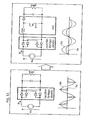
- FIG 6 is a diagram illustrating an example of the voltage-dividing bridgeless PFC circuit 1.
- FIG 7 is a diagram illustrating an effect of the voltage-dividing bridgeless PFC circuit.
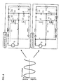
- INPUT VOLTAGE in FIG. 7 represents a plot of an AC voltage applied from the external power source 6.
- INPUT CURRENT represents a plot of a current input in the voltage-dividing bridgeless PFC circuit.
- POSITIVE OUTPUT TERMINAL VOLTAGE represents a plot of a voltage applied to the positive output terminal depicted in FIG. 6 .
- NEGATIVE OUTPUT TERMINAL VOLTAGE is a plot of a voltage applied to the negative output terminal depicted in FIG 6 .
- OUTPUT VOLTAGE is a plot of the difference between positive and negative outputs.
- the inductance of each of inductors L1 and L2 is 220 ⁇ H
- the capacitance of each of capacitors C1 and C2 is 450 ⁇ F
- a resistance of 5 m ⁇ is connected to FETs Q1 and Q2.
- Critical mode PFC control circuits in FIG. 6 are circuits having functions similar to those of the PWM control circuits 8 and 9.
- the voltage-dividing bridgeless PFC circuit 1 may reduce a voltage applied to the components of each of the power factor correction circuits 2 and 3 to half a voltage applied in a conventional PFC circuit and yet may output a voltage equivalent to that of the conventional PFC circuit.
- the voltage-dividing bridgeless PFC circuit 1 includes the circuit including the first power factor correction circuit 2 that improves the power factor when a positive AC voltage is input from the external power source 6 and the second power factor correction circuit 3 that is connected with the first power factor correction circuit 3 in parallel and that improves the power factor when a negative AC voltage is applied from the external power source 6.
- the voltage-dividing bridgeless PFC circuit 1 may improve the power factor of supplied AC power without using a bridge diode. Consequently, the voltage-dividing bridgeless PFC circuit 1 may reduce power loss.
- the voltage-dividing bridgeless PFC circuit 1 may reduce a boosted voltage in each of the power factor correction circuits 2 and 3 to half compared with a conventional PFC circuit and therefore may use low-voltage components. Since the voltage-dividing bridgeless PFC circuit 1 may use low-voltage components, which are small, the footprint of the voltage-dividing bridgeless PFC circuit 1, and therefore the footprint of the PSU, may be reduced.
- the voltage-dividing bridgeless PFC circuit 1 includes the output circuit 4 that includes the capacitors C 1 and C2 provided in series, voltages output from the power factor correction circuits 2 and 3 may be added together. That is, the voltage-dividing bridgeless PFC circuit 1 reduces a boosted voltage in each of the power factor correction circuits 2 and 3 to half compared with a conventional PFC circuit and yet may output a voltage equivalent to that of the conventional PFC circuit.
- the voltage-dividing bridgeless PFC circuit 1 turns off the PWM control circuit 9 when the PWM control circuit 8 operates, and turns off the PWM control circuit 8 when the PWM control circuit 9 operates.
- the voltage-dividing bridgeless PFC circuit 1 may reduce power consumed by the control circuit 5.
- a voltage-dividing bridgeless PFC circuit 1 described above has independent inductors L1 and L2 provided in the first and second power factor correction circuits 2 and 3, respectively.
- the present invention is not limited to the embodiment.
- a voltage-dividing bridgeless PFC circuit 1 a according to the present embodiment may have a circuit in which a first power factor correction circuit 2a and a second power factor correction circuit 3a according to the second embodiment share one single inductor.
- FIG. 8 is a diagram illustrating reduction of the number of boost inductors and current transformers.
- a first power factor correction circuit 2a and a second power factor correction circuit 3a of the second embodiment share an inductor L3 for boosting an applied positive AC voltage.
- the first power factor correction circuit 2a improves the power factor of electric power only when a positive AC voltage is applied
- the second power factor correction circuit 3a improves the power factor of electric power only when a negative AC voltage is applied. That is, the first and second power factor correction circuits 2a and 3a use the inductor L3 at different timings.
- first and second power correction circuits 2a and 3a may share the inductor L3. Consequently, the number of inductors used in the voltage-dividing bridgeless PFC circuit 1 a is reduced and therefore the size and cost of the circuit may be reduced. In addition, the reduction in equivalent series resistance (ESR) in the voltage-dividing bridgeless PFC circuit 1 a may improve the efficiency of the circuit.
- ESR equivalent series resistance
- the voltage-dividing bridgeless PFC circuit 1 described above includes the PWM control circuit 8 that controls the first power factor correction circuit 2 and the PWM control circuit 9 that controls the second power factor correction circuit 3.
- the present invention is not limited to the embodiment.
- a voltage-dividing bridgeless PFC circuit 1b according to the second embodiment may include a PWM control circuit 23 that controls the first and second power factor correction circuits 2a and 3a at the same time.
- FIG 9 is a diagram illustrating a circuit in which a PWM control circuit is shared.
- a control circuit 5a illustrated in FIG. 9 includes a PWM control circuit 23.
- the PWM control circuit 23 has a function similar to that of the PWM control circuit 8 of the first embodiment.
- the PWM control circuit 23 transmits the same gate voltage to FETs Q1 and Q2 at the same time.
- the voltage-dividing bridgeless PFC circuit 1b may appropriately improve the power factor of electric power even though the FET Q1 of the first power factor correction circuit 2a and the FET Q2 of the second power factor correction circuit 3a are controlled at the same time. Since the number of PWM control circuits may be reduced, the size and cost of the voltage-dividing bridgeless PFC circuit 1b may be reduced.
- the voltage-dividing bridgeless PFC circuit 1 described above includes the diode D1 that allows current to flow though the first power factor correction circuit 2 in a constant direction.
- the voltage-dividing bridgeless PFC circuit 1 also includes the diode D2 that allows current to flow through the second power factor correction circuit 3 in a constant direction.
- the present invention is not limited to the embodiment.
- a voltage-dividing bridgeless PFC circuit 1c according to the second embodiment may include FETs Q3 and Q4 in place of the diodes D1 and D2, respectively.
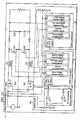
- FIG. 10 illustrates an exemplary voltage-dividing bridgeless PFC circuit that includes a further reduced number of diodes.
- the voltage-dividing bridgeless PFC circuit 1c has circuits that include FETs Q3 and Q4 in place of the diodes D1 and D2, respectively, of the first embodiment.
- the gate of the FET Q3 is connected to a circuit point at which an AC input polarity determination circuit 7 applies a voltage to a PWM control circuit 8.
- the gate of the FET Q4 is connected to a circuit point at which the AC input polarity determination circuit 7 applies a voltage to a PWM control circuit 9.
- the AC input polarity determination circuit 7 of the second embodiment acts as a voltage application control circuit that applies a gate voltage to the FET Q3 when the AC input polarity determination circuit 7 has detect a positive AC current and applies a gate voltage to the FET Q4 when it has detected a negative AC current.
- the first power factor correction circuit 2a includes the FET Q3 that allows current to flow through the first power factor correction circuit 2a only when a gate voltage is applied by the control circuit 5b, so that the current flowing through the FET Q3 is forced to be in phase with the positive AC voltage to improve the power factor of electric power.
- the second power factor correction circuit 3a includes the FET Q4 that allows current to flow through the second power factor correction circuit 3a only when a gate voltage is applied by the control circuit 5b, so that the current flowing through the FET Q4 is forced to be in phase with the negative AC voltage to improve the power factor of electric power.
- the voltage-dividing bridgeless PFC circuit 1c uses FETs to replace diodes, power loss may be further reduced. Furthermore, a voltage that is applied from the AC input polarity determination circuit 7 for causing the PWM control circuits 8 and 9 to operate is used to cause the FETs 3 and 4 to operate, the voltage-dividing bridgeless PFC circuit 1c does not need a control circuit for causing the FETs Q3 and Q4 to operate. Consequently, the voltage-dividing bridgeless PFC circuit 1c may reduce power loss without increasing the size of the circuit.
Abstract
A circuit (1) include: a first power factor correction circuit (2) that forces current produced by the positive AC voltage to be in phase with the positive AC voltage so that a power factor of electric power is improved; a second power factor correction circuit (3) that forces current produced by the negative AC voltage to be in phase with the negative AC voltage so that a power factor of electric power is improved; and an output circuit (4) including a first capacitor (C1) storing first electric power with a power factor improved by the first power factor correction circuit and a second capacitor (C2) storing second electric power with a power factor improved by the second power factor correction circuit, the first capacitor (C1) and the second capacitor (C2) being provided in series, the output circuit (4) outputting the first electric power stored in the first capacitor (C1) and the second electric power stored in the second capacitor (C2).
Description
- The present invention relates to a voltage-dividing power factor correction circuit, a voltage-dividing power factor correction apparatus, and a voltage-dividing power factor correction method.
- Power Supply Units (PSUs) designed to convert an input alternating current (AC) voltage to a direct current (DC) voltage are used for supplying power to computers such as servers and personal computers. Such a PSU may cause noise and distribution loss because rectifiers and smoothing capacitors provided in the PSU distort the waveform of an input current. Therefore, a Power Factor Correction (PFC) circuit, which improves the power factor of input electric power (electrical current) to prevent noise and reduce distribution loss, is incorporated in PSUs to confirm to the IEC 1000_3_4 standard.
- Referring to
FIGS. 11 and12 , an example of PSU will be described. FIG II illustrates a configuration of a PSU.FIG. 12 illustrates a PFC circuit. An input AC voltage in the range of 110 V to 240 V, for example, is applied to the PSU illustrated inFIG. 11 . A rectifier in the PSU rectifies the applied AC voltage. The rectified voltage is applied to the PFC circuit. A DC-DC conversion circuit in the PSU converts the DC voltage of 380 V (volts) with a power factor improved by the PFC circuit to a DC voltage of 12 V, which is then supplied to a computer such as a server or a personal computer.
In the PSU illustrated in the left-hand part ofFIG. 12 , a distorted current Iin flows because no PFC circuit is provided. In contrast, in the PSU illustrated in the right-hand part ofFIG. 12 , a PFC circuit brings the waveform of the current Iin into phase with the waveform of an input voltage Vin to reduce distortion of the current Iin, thereby reducing noise and distribution loss. - The PFC circuit brings the waveform of an input current closer to a sinusoidal waveform to reduce distortion of the current to improve the power factor of the input electric power. Specifically, when a voltage rectified by the rectifier is applied, the PFC circuit uses high-frequency switching and pulse width modulation to form a current waveform that is closer to the waveform of the input voltage.
- Referring to
FIGS. 13 and14 , how a PFC circuit improves a power factor will be described.FIG. 13 3 illustrates a method for improving a power factor.FIG. 14 illustrates the effect of the PFC circuit. The PFC circuit in the example inFIG. 13 includes a control circuit that drives a field effect transistor (FET) according to an input voltage and an input current. - When a voltage rectified by a bridge diode, which functions as a rectifier, is applied to the PFC circuit, the PFC circuit intermittently turns on the FET to allow current to flow alternately through a path (1) in
FIG. 13 and a path (2) inFIG. 13 . As illustrated inFIG. 14 , the PFC circuit then adds the intermittent current flowing through the path (I) and the intermittent current flowing through the path (2) together to bring the waveform of the input current closer to the waveform of the rectified voltage. - Here, power loss is caused in the PSU by the bridge diode functioning as the rectifier. For example, a PSU in an example illustrated in
FIG. 15 uses a bridge diode to allow current to flow through the PFC circuit in a constant direction. Specifically, the PSU inevitably includes two diodes in a path through which current flows, which cause power loss.FIG 15 is a diagram for explaining power loss in the bridge diode. - High-voltage capacitors and FETs are provided in a PFC circuit because an input voltage increases in the course of correction of the power factor.
FIG. 16 illustrates resistances of FETs. As illustrated inFIG. 16 , high-voltage FETs have larger current resistances than low-voltage FETs. In addition, high-voltage capacitors and FETs are larger in size than low-voltage capacitors and FETs. Accordingly, a PSU incorporating a PFC circuit has a higher equivalent resistance and a larger footprint than a PSU without a PFC circuit. - A power factor correction technique using synchronous rectification is known in which a bridge diode is replaced with multiple FETs and a control integrated circuit (IC) in order to avoid the power loss in diodes described above (
US Patent No. 7164591 , National Publication of International Patent ApplicationWO 2007-527687 ). For example, a PSU using synchronous rectification in an example illustrated inFIG. 17 7 uses four FETs and a control integrated circuit (IC) to replace a bridge diode in order to reduce power loss. - An interleaved power factor correction technique is known in which PFC circuits are provided in parallel in order to reduce equivalent series resistance (ESR) caused by the PFC circuits. For example, a PSU using interleaved circuitry in an example illustrated in
FIG. 18 includes a bridge diode functioning as a rectifier and two PFC circuits provided in parallel. Such a PSU applies a voltage rectified by the bridge diode to the two parallel PFC circuits at the same time to reduce ESR in the PFC circuits to half. The PSU also reduces ripple current by controlling the parallel PFC circuits so as to operate 180 degrees out of phase with each other. - However, the power factor correction technique using synchronous rectification described above has the problem of increase in the footprint of the PSU resulting from the increase in the footprint of the rectifier because the diodes of the bridge diode are replaced with FETs and a control IC for controlling the FETs is added. For example, in the example illustrated in
FIG. 17 , one bridge diode is replaced with four FETs and a control IC for controlling the FETs is added, resulting in an increased footprint of the rectifier. - With the interleaved power factor correction technique described above, an input voltage applied to each PFC circuit increases. Therefore high-voltage capacitors and high-voltage FETs are provided in each PFC circuit. As a result, the footprints of the PFC circuits, and therefore the foot print of the PSU, increase. Another problem with the technique is that since a bridge diode, which functions as a rectifier, is provided in the PSU, power loss occurs in each diode of the bridge diode.
- In one aspect of the present invention, the present invention reduces the footprint of a PSU or reduces power loss in a PSU.
- According to one aspect of the embodiments, there is provided a voltage-dividing power factor correction circuit includes a first power factor correction circuit that, when a positive AC voltage is applied from an external source, forces current produced by the applied positive AC voltage to be in phase with the applied positive AC voltage so that a power factor of electric power is improved; a second power factor correction circuit that, when a negative AC voltage is applied from an external source, forces current produced by the applied negative AC voltage to be in phase with the applied negative AC voltage so that a power factor of electric power is improved; and an output circuit including a first capacitor storing first electric power with a power factor improved by the first power factor correction circuit and a second capacitor storing second electric power with a power factor improved by the second power factor correction circuit, the first capacitor and the second capacitor being provided in series, the output circuit outputting the first electric power stored in the first capacitor and the second electric power stored in the second capacitor.
Reference is made, by way of example only, to the accompanying drawings in which: -
-
FIG. 1 is a diagram illustrating a voltage-dividing bridgeless PFC circuit according to a first embodiment; -
FIG 2 is a diagram illustrating a control circuit; -
FIG 3 is a diagram illustrating exemplary timings at which the control circuit controls FETs; -
FIG. 4 is a diagram illustrating an exemplary process performed by a voltage-dividing bridgeless PFC circuit to improve a power factor; -
FIG 5 is a diagram illustrating voltage and current values in a voltage-dividing bridgeless PFC circuit; -
FIG. 6 is a diagram illustrating an exemplary voltage-dividing bridgeless PFC circuit; -
FIG. 7 is a diagram illustrating an effect of the voltage-dividing bridgeless PFC circuit; -
FIG. 8 is a diagram illustrating reduction of the number of boost inductors and current transformers; -
FIG. 9 is a diagram illustrating circuits that share a PWM control circuit; -
FIG 10 is a diagram illustrating an exemplary voltage-dividing bridgeless PFC circuit in which the number of diodes are further reduced; -
FIG. 11 is a diagram illustrating a configuration of a PSU; -
FIG. 12 is a diagram illustrating a PFC circuit; -
FIG. 13 is a diagram illustrating a method for improving a power factor; -
FIG. 14 is a diagram illustrating an effect of the PFC circuit; -
FIG. 15 is a diagram illustrating power loss in a bridge diode; -
FIG. 16 is a diagram illustrating the resistances of FETs; -
FIG. 17 is a diagram illustrating a technique that replaces a bridge diode with FETs; and -
FIG. 18 is a diagram illustrating a technique that uses interleaving. - A voltage-dividing power factor correction circuit of the present application will be described with reference to the accompanying drawings.
- An example of voltage-dividing power factor correction (PFC) circuit of a first embodiment will be described with reference to
FIG 1. FIG 1 illustrates a voltage-dividing bridgeless PFC circuit according to the first embodiment. The voltage-dividing bridgeless PFC circuit includes at least two power factor correction circuits provided in parallel. - As illustrated in
FIG 1 , the voltage-dividingbridgeless PFC circuit 1 includes a first powerfactor correction circuit 2, a second powerfactor correction circuit 3, anoutput circuit 4, and acontrol circuit 5 and is connected to anexternal power source 6 and an external resistance R1. Theexternal power source 6 is an AC power source which applies an AC voltage to the voltage-dividingbridgeless PFC circuit 1 . - When a positive AC voltage is applied from the
external power source 6, the first powerfactor correction circuit 2 forces current produced by the applied positive AC voltage to be in phase with the applied positive AC voltage to improve the power factor of electric power. When a positive AC voltage is applied from theexternal power source 6, the first powerfactor correction circuit 2 uses a FET Q1 to force the current produced by the applied positive AC voltage to be in phase with the applied positive AC voltage to improve the power factor of electric power. - That is, the first power
factor correction circuit 2 allows current I1 to flow through itself only when a positive AC voltage is applied from theexternal power source 6. Accordingly, the first powerfactor correction circuit 2 forces the current 11 to be in phase with the applied positive AC voltage to improve the power factor of electric power only when the positive AC voltage is applied from theexternal power source 6. The first powerfactor correction circuit 2 then stores the electric power with the improve power factor in acapacitor C 1. - The first power
factor correction circuit 2 is connected to theexternal power source 6 in parallel with the second powerfactor correction circuit 3, which will be described later. Therefore and because current flows through the first powerfactor correction circuit 2 only when a positive voltage is applied from theexternal power source 6, half the AC voltage applied from theexternal power source 6 is applied to the first powerfactor correction circuit 2. This means that the first powerfactor correction circuit 2 may use low-voltage components which are smaller than high-voltage components and therefore may have a smaller footprint than a power factor correction circuit that uses high-voltage components. - When a negative AC voltage is applied from the
external power source 6, the second powerfactor correction circuit 3 forces current produced by the applied negative AC voltage to be in phase with the applied negative AC voltage to improve the power factor of electric power. When a negative AC voltage is applied from theexternal power source 6, the second powerfactor correction circuit 3 uses a FET Q2 to force current produced by the applied negative AC voltage to be in phase with the applied negative AC voltage to improve the power factor of the electric power. - That is, the second power
factor correction circuit 3 allows current 12 to flow through itself only when a negative AC voltage is applied from theexternal power source 6. Accordingly, the second powerfactor correction circuit 3 forces the current 12 to be in phase with the applied negative AC voltage to improve the power factor of electric power only when the negative AC voltage is applied from theexternal power source 6. The second powerfactor correction circuit 3 then stores the electric power with the improve power factor in a capacitor C2. - The second power
factor correction circuit 3 is connected to theexternal power source 6 in parallel with the first powerfactor correction circuit 2. Therefore and because current flows through the second powerfactor correction circuit 3 only when a negative voltage is applied from theexternal power source 6, half the applied voltage from theexternal power source 6 is applied to the components of the second powerfactor correction circuit 3. This means that the second powerfactor correction circuit 3 may use components having half the withstand voltage of conventional ones. Consequently, the footprint of the power factor correction circuit may be reduced compared with a conventional power factor correction circuit. - The
output circuit 4 has the capacitors C1 and C2 connected in series. Thecapacitor C 1 stores electric power with a power factor improved by the first powerfactor correction circuit 2, whereas the capacitor C2 stores electric power with a power factor improved by the second powerfactor correction circuit 3. Theoutput circuit 4 outputs the electric power stored in thecapacitors C 1 and C2 connected in series to the external resistance R1. - The
control circuit 5 detects whether an AC voltage applied from theexternal power source 6 is positive or negative. When thecontrol circuit 5 detects a positive AC voltage applied from theexternal power source 6, thecontrol circuit 5 applies a gate voltage to the FET Q1 of the first powerfactor correction circuit 2; when thecontrol circuit 5 detects a negative AC voltage applied from theexternal power source 6, thecontrol circuit 5 applies a gate voltage to the FET Q2 of the second powerfactor correction circuit 3. - That is, when a positive voltage is applied from the
external power source 6, thecontrol circuit 5 intermittently turns on theFET Q 1 of the first power factor correction circuit to cause the first powerfactor correction circuit 2 to improve the power factor of electric power; when a negative voltage is applied from theexternal power source 6, thecontrol circuit 5 intermittently turns on the FET Q2 of the second powerfactor correction circuit 3 to cause the second powerfactor correction circuit 3 to improve the power factor of electric power. - As described above, the voltage-dividing
bridgeless PFC circuit 1 includes the first powerfactor correction circuit 2 that, when a positive AC voltage is applied, forces current produced by the applied positive voltage to be in phase with the applied positive voltage to improve the power factor of electric power. The voltage-dividingbridgeless PFC circuit 1 also includes the second powerfactor correction circuit 3 that is provided in parallel with the first powerfactor correction circuit 2 and, when a negative AC voltage is applied, forces current produced by the applied negative voltage to be in phase with the applied negative voltage to improve the power factor of electric power. - That is, the voltage-dividing
bridgeless PFC circuit 1 includes a circuit including the first powerfactor correction circuit 2 that improves the power factor only when a positive AC voltage is applied from theexternal power source 6 and the second powerfactor correction circuit 3 that is connected in parallel with the first powerfactor correction circuit 2 and that improves the power factor only when a negative AC voltage is applied from theexternal power source 6. Therefore, the voltage-dividingbridgeless PFC circuit 1 may improve the power factor of supplied AC power without using a bridge diode. - A conventional PSU used a bridge diode, for example, to allow the current to flow through a PFC circuit in a constant direction. Therefore, there were three diodes in a current path in the example illustrated in
FIG 15 . On the other hand, the voltage-dividingbridgeless PFC circuit 1 in the example illustrated inFIG 1 includes the first powerfactor correction circuit 2 through which current flows when a positive voltage is applied from theexternal power source 6 and the second powerfactor correction circuit 3 through which current flows when a negative voltage is applied from theexternal power source 6. - Accordingly, the voltage-dividing
bridgeless PFC circuit 1 does not need a bridge diode for maintaining the direction of current flowing through the PFC circuit constant and therefore may reduce the number of diodes in a current path to two. That is, the voltage-dividingbridgeless PFC circuit 1 may reduce power loss caused by a bridge diode. - Only a positive AC voltage is applied to the first power
factor correction circuit 2 whereas only a negative AC voltage is applied to the second powerfactor correction circuit 3. That is, only half the AC voltage supplied from theexternal power source 6 is applied to each of the powerfactor correction circuits factor correction circuits bridgeless PFC circuit 1 may use small, low-voltage components, the footprint of the voltage-dividingbridgeless PFC circuit 1, and therefore the footprint of the PSU, may be reduced. - Since the voltage-dividing
bridgeless PFC circuit 1 includes theoutput circuit 4 includingcapacitors C 1 and C2 provided in series, the voltage-dividingbridgeless PFC circuit 1 may add voltages output from the powerfactor correction circuits bridgeless PFC circuit 1 reduces a boosted voltage in each of the powerfactor correction circuit - Components of the voltage-dividing
bridgeless PFC circuit 1 will be described below. The first powerfactor correction circuit 2 includes a diode D1, an inductor (coil) L1, a field effect transistor (FET) Q1, a diode D3, and a capacitor C1. The first powerfactor correction circuit 2 has a closed circuit through which current flows from theexternal power source 6 to the diode D1 to the inductor L1 and to the FET Q1 when a positive AC voltage is applied from theexternal power source 6. The first powerfactor correction circuit 2 has a closed circuit through which current flows from theexternal power source 6 to the diode D1 to the inductor L1 to the diode D3 to the capacitor C1 when a positive AC voltage is applied from theexternal power source 6. - The FET Q1 is a field effect transistor that forces current to flow from the inductor L1 toward the
external power source 6 when a gate voltage Vgs1 is applied from thecontrol circuit 5, which will be described later, to the FET Q1. The FET Q1 does not allow current to flow from theinductor L 1 toward theexternal power source 6 when thegate voltage Vgs 1 is not applied. - The diode D1 is a diode that allows current to flow from the
external power source 6 toward the inductor L1. The inductor L1 is a passive element designed to have a specific amount of inductance. The diode D3 is a diode that allows current to flow from the inductor L1 toward the capacitor C1. Thecapacitor C 1 is a capacitor that stores electric power having an improved power factor. - The second power
factor correction circuit 3 includes a diode D2, an inductor L2, a FET Q2, a diode D4 and a capacitor C2. The second powerfactor correction circuit 3 has a closed circuit through which current flows from the FET Q2 to the inductor L2 to the diode D2 when a negative AC voltage is applied from theexternal power source 6. The second powerfactor correction circuit 3 has a closed circuit through which current flows from theexternal power source 6 to the capacitor C2 to the diode D4 to the inductor L2 to the diode D2 when a negative AC voltage is applied from theexternal power source 6. - The FET Q2 is a field effect transistor that allows current to flow from the
external power source 6 toward the inductor L2 when a gate voltage Vgs2 is applied from thecontrol circuit 5, which will be described later, to the FET Q2. The FET Q2 does not allow current to flow from theexternal power source 6 toward the inductor L2 when the gate voltage Vgs2 is not applied. - The diode D2 is a diode that allows current to flow from the inductor L2 toward the
external power source 6. The inductor L2 is an inductor similar to the inductor L1. The diode D4 is a diode that allows current to flow from the capacitor C2 toward the inductor L2. The capacitor C2 is a capacitor that stores electric power having an improved power factor. The capacitor C2 is connected to the external resistance R1 in series with thecapacitor C 1. - The
control circuit 5 will be described in detail with reference toFIG. 2 , which is a diagram illustrating thecontrol circuit 5. Thecontrol circuit 5 in the example illustrated inFIG. 2 includes an AC input polarity determination circuit 7, and pulse width modulation (PWM)control circuits 8 and 9. The AC input polarity determination circuit 7 includescomparators - The
PWM control circuit 8 includes an ON/OFF switch 12, an inputvoltage monitor circuit 13, acurrent monitor circuit 14, a FET drivesignal output circuit 15, and an outputvoltage monitor circuit 16. The PWM control circuit 9 includes an ON/OFF switch 17, an inputvoltage monitor circuit 18, acurrent monitor circuit 19, a FET drivesignal output circuit 20, and an outputvoltage monitor circuit 21. - Operations of the circuits of the
control circuit 5 will be described below. The AC input polarity determination circuit 7 detects the polarity of an AC voltage applied from theexternal power source 6. When the AC input polarity determination circuit 7 detects a positive AC voltage, the AC input polarity determination circuit 7 applies a predetermined voltage to thePWM control circuit 8; when the AC input polarity determination circuit 7 detects a negative AC voltage, the AC input polarity determination circuit 7 applies a predetermined voltage to the PWM control circuit 9. - The
PWM control circuit 8 measures the value of input voltage applied from theexternal power source 6 to the first powerfactor correction circuit 2. ThePWM control circuit 8 also measures the value of current flowing in the inductor L1. ThePWM control circuit 8 measures the value of output voltage between the capacitor C1 and the external resistance R1. - When a voltage is applied from the AC input polarity determination circuit 7 to the
PWM control circuit 8, thePWM control circuit 8 intermittently applies the gate voltage Vgs1 to the FET Q1 according to the measured input voltage value, current value and output voltage value. - The PWM control circuit 9 measures the value of input voltage applied from the
external power source 6 to the second powerfactor correction circuit 3. The PWM control circuit 9 measures the value of current flowing in the inductor L2. The PWM control circuit 9 also measures the value of output voltage between the capacitor C1 and the external resistance R1. - When a voltage is applied from the AC input polarity determination circuit 7 to the PWM control circuit 9, the PWM control circuit 9 intermittently applies the gate voltage Vgs2 to the FET Q1 according to the measured input voltage value, current value and output voltage value. That is, when a negative voltage is applied from the
external power source 6 to the second powerfactor correction circuit 3, the PWM control circuit 9 intermittently turns on the FET Q2 to cause the second powerfactor correction circuit 3 to improve the power factor of electric power. - The components of the AC input polarity determination circuit 7 and the components of the
PWM control circuits 8 and 9 will be described below. When a positive AC voltage is applied from theexternal power source 6, thecomparator 10 applies a predetermined voltage to the ON/OFF switch 12 of thePWM control circuit 8. On the other hand, when a negative AC voltage is applied from theexternal power source 6, thecomparator 11 transmits a predetermined voltage to the ON/OFF switch 17 of the PWM control circuit 9. - When the predetermined voltage is applied to the ON/
OFF switch 12 of thePWM control circuit 8, the ON/OFF switch 12 causes thecircuits 13 through 16 to operate. The inputvoltage monitor circuit 13 measures the value of an input voltage applied to the first powerfactor correction circuit 2. Thecurrent monitor circuit 14 measures the value of current flowing in the inductor L1. The outputvoltage monitor circuit 16 measures the value of an external voltage between the capacitor C1 and the external resistance R1. The FET drivesignal output circuit 15 intermittently applies the gate voltage Vgs1 to the FET Q1 according to the measured input voltage value, current value and external voltage value. - On the other hand, when the predetermined voltage is applied to the ON/
OFF switch 17 of the PWM control circuit 9, the ON/OFF switch 17 causes thecircuits 18 through 21 to operate. The inputvoltage monitor circuit 18 measures the value of input voltage applied to the second powerfactor correction circuit 3. Thecurrent monitor circuit 19 measures the value of current flowing in the inductor L2. The outputvoltage monitor circuit 21 measures the value of an external voltage between the capacitor C1 and the external resistance R1. The FET drivesignal output circuit 20 intermittently applies the gate voltage Vgs2 to the FET Q2 according to the measured input voltage value, current value and external voltage value. - Referring to
FIG. 3 , the timings at which thecontrol circuit 5 controls the FETs Q and Q2 will be described below.FIG 3 is a diagram illustrating exemplary timings at which the control circuit controls the FETs. AC INPUT inFIG. 3 represents the level of AC voltage applied from theexternal power source 6, ranging from -144 V to +144 V. - CONTROL OUTPUT A in
FIG. 3 represents the level of voltage output from thecomparator 10. CONTROL OUTPUT A' represents the level of voltage applied from thecomparator 10 to the ON/OFF switch 12 of thePWM control circuit 8 through a diode. CONTROL OUTPUT B represents the level of voltage output from thecomparator 11. CONTROL OUTPUT B' represents the level of voltage applied from thecomparator 11 to the ON/OFF switch 17 of the PWM control circuit 9 through a diode. - For example, when AC INPUT in the example in
FIG. 3 is positive, CONTROL OUTPUT A is positive and CONTROL OUTPUT A' is at a predetermined voltage value VCC. Therefore thePWM control circuit 8 turns on and the FET Q1 intermittently turns on. On the other hand, the PWM control circuit 9 does not turn on because CONTROL OUTPUT B is negative and CONTROL OUTPUT B' is not output when AC INPUT is positive. - When AC INPUT is negative, CONTROL OUTPUT B is positive and CONTROL OUTPUT B' is at a predetermined voltage value VCC. Therefore, the PWM control circuit 9 turns on and the FET Q2 intermittently turns on. The
PWM control circuit 8, on the other hand, does not turn on because CONTROL OUTPUT A is negative and CONTROL OUTPUT A' is not output when AC INPUT is negative. - Referring to
FIG 4 , an exemplary process performed by the voltage-dividingbridgeless PFC circuit 1 to improve the power factor will be described below.FIG. 4 is a diagram illustrating the exemplary process performed by the voltage-dividing bridgeless PFC circuit for improving the power factor. When a positive AC voltage is applied from theexternal power source 6 to the voltage-dividingbridgeless PFC circuit 1 in the example illustrated inFIG. 4 , current 11 flows through the first powerfactor correction circuit 2. - When the current 11 flows through the first power
factor correction circuit 2, the first powerfactor correction circuit 2 intermittently switches between paths (1) and (2) illustrated inFIG. 4 to allow the current 11 flowing through the first powerfactor correction circuit 2 to be in phase with the applied voltage. That is, the first powerfactor correction circuit 2 improves the power factor of electric power when a positive AC voltage is applied from theexternal power source 6. The first powerfactor correction circuit 2 then stores the electric power with the improved power factor in thecapacitor C 1. Thecapacitor C 1 then supplies the stored electric power to path (5). - On the other hand, when a negative AC voltage is applied from the
external power source 6 to the voltage-dividingbridgeless PFC circuit 1, current 12 flows through the second powerfactor correction circuit 3. When the current 12 flows through the second powerfactor correction circuit 3, the second powerfactor correction circuit 3 intermittently switches between paths (3) and (4) illustrated inFIG 4 to force the current 12 flowing through the second powerfactor correction circuit 3 to be in phase with the applied voltage. That is, when a negative AC voltage is applied from theexternal power source 6, the second powerfactor correction circuit 3 improves the power factor of electric power. The second powerfactor correction circuit 3 then stores the electric power with the improved power factor in the capacitor C2. The capacitor C2 then supplies the stored electric power to path (5). - Referring to
FIG 5 , voltages output from the voltage-dividingbridgeless PFC circuit 1 will be described below.FIG 5 is a diagram illustrating voltage and current values in the voltage-dividing bridgeless PFC circuit. InFIG 5 , V represents a voltage applied from the capacitor C1 to the external resistance R1 and V2 represents a voltage applied from the capacitor C2 to the external resistance R1. In the example illustrated inFIG. 5 , each of the capacitors C1 and C2 applies a voltage of 190 V to the external resistance R1. - The capacitors C1 and C2 in the voltage-dividing
bridgeless PFC circuit 1 are provided in series with the external resistance R1. Therefore, the voltage applied by the voltage-dividing bridgeless PFC circuit I to the external resistance R1 is 380 V That is, the voltage-dividingbridgeless PFC circuit 1 reduces the boosted voltage in the first and second powerfactor correction circuits - Referring to
FIGS. 6 and7 , a specific example of the voltage-dividingbridgeless PFC circuit 1 will be described below.FIG 6 is a diagram illustrating an example of the voltage-dividingbridgeless PFC circuit 1.FIG 7 is a diagram illustrating an effect of the voltage-dividing bridgeless PFC circuit. INPUT VOLTAGE inFIG. 7 represents a plot of an AC voltage applied from theexternal power source 6. INPUT CURRENT represents a plot of a current input in the voltage-dividing bridgeless PFC circuit. POSITIVE OUTPUT TERMINAL VOLTAGE represents a plot of a voltage applied to the positive output terminal depicted inFIG. 6 . NEGATIVE OUTPUT TERMINAL VOLTAGE is a plot of a voltage applied to the negative output terminal depicted inFIG 6 . OUTPUT VOLTAGE is a plot of the difference between positive and negative outputs. - In the example illustrated in
FIG. 6 , the inductance of each of inductors L1 and L2 is 220 µH, the capacitance of each of capacitors C1 and C2 is 450 µF, and a resistance of 5 mΩ is connected to FETs Q1 and Q2. Critical mode PFC control circuits inFIG. 6 are circuits having functions similar to those of thePWM control circuits 8 and 9. - When an AC voltage of 100 V was applied from the
external power source 6 to the voltage-dividingbridgeless PFC circuit 1 illustrated inFIG. 6 , the outputs illustrated inFIG. 7 resulted. It may be seen from the example inFIG. 7 that the input voltage and the input current have the same waveforms and an output voltage of 380 V may be obtained. This shows that the voltage-dividingbridgeless PFC circuit 1 may reduce a voltage applied to the components of each of the powerfactor correction circuits - As has been described above, the voltage-dividing
bridgeless PFC circuit 1 includes the circuit including the first powerfactor correction circuit 2 that improves the power factor when a positive AC voltage is input from theexternal power source 6 and the second powerfactor correction circuit 3 that is connected with the first powerfactor correction circuit 3 in parallel and that improves the power factor when a negative AC voltage is applied from theexternal power source 6. With the configuration, the voltage-dividingbridgeless PFC circuit 1 may improve the power factor of supplied AC power without using a bridge diode. Consequently, the voltage-dividingbridgeless PFC circuit 1 may reduce power loss. - Furthermore, current flows through the first power
factor correction circuit 2 only when a positive AC voltage is applied, whereas current flows through the second powerfactor correction circuit 3 only when a negative AC voltage is applied. That is, only half of the AC voltage applied from theexternal power source 6 performs work in each of the powerfactor correction circuits bridgeless PFC circuit 1 may reduce a boosted voltage in each of the powerfactor correction circuits bridgeless PFC circuit 1 may use low-voltage components, which are small, the footprint of the voltage-dividingbridgeless PFC circuit 1, and therefore the footprint of the PSU, may be reduced. - Furthermore, since the voltage-dividing
bridgeless PFC circuit 1 includes theoutput circuit 4 that includes thecapacitors C 1 and C2 provided in series, voltages output from the powerfactor correction circuits bridgeless PFC circuit 1 reduces a boosted voltage in each of the powerfactor correction circuits - Furthermore, the voltage-dividing
bridgeless PFC circuit 1 turns off the PWM control circuit 9 when thePWM control circuit 8 operates, and turns off thePWM control circuit 8 when the PWM control circuit 9 operates. Thus, the voltage-dividingbridgeless PFC circuit 1 may reduce power consumed by thecontrol circuit 5. - While an embodiment of the present invention has been described, the present invention may be carried out in various modes besides the embodiment described above. Another example which falls in the scope of the present invention will be described below as a second embodiment.
- In the voltage-dividing
bridgeless PFC circuit 1 described above has independent inductors L1 and L2 provided in the first and second powerfactor correction circuits factor correction circuit 2a and a second powerfactor correction circuit 3a according to the second embodiment share one single inductor. -
FIG. 8 is a diagram illustrating reduction of the number of boost inductors and current transformers. In the example illustrated inFIG. 8 , a first powerfactor correction circuit 2a and a second powerfactor correction circuit 3a of the second embodiment share an inductor L3 for boosting an applied positive AC voltage. The first powerfactor correction circuit 2a improves the power factor of electric power only when a positive AC voltage is applied, whereas the second powerfactor correction circuit 3a improves the power factor of electric power only when a negative AC voltage is applied. That is, the first and second powerfactor correction circuits - Thus the first and second
power correction circuits - The voltage-dividing
bridgeless PFC circuit 1 described above includes thePWM control circuit 8 that controls the first powerfactor correction circuit 2 and the PWM control circuit 9 that controls the second powerfactor correction circuit 3. However, the present invention is not limited to the embodiment. For example, a voltage-dividing bridgeless PFC circuit 1b according to the second embodiment may include aPWM control circuit 23 that controls the first and second powerfactor correction circuits -
FIG 9 is a diagram illustrating a circuit in which a PWM control circuit is shared. Acontrol circuit 5a illustrated inFIG. 9 includes aPWM control circuit 23. ThePWM control circuit 23 has a function similar to that of thePWM control circuit 8 of the first embodiment. ThePWM control circuit 23 transmits the same gate voltage to FETs Q1 and Q2 at the same time. - Current follows through the first and second power
factor correction circuits factor correction circuit 2a and the FET Q2 of the second powerfactor correction circuit 3a are controlled at the same time. Since the number of PWM control circuits may be reduced, the size and cost of the voltage-dividing bridgeless PFC circuit 1b may be reduced. - The voltage-dividing
bridgeless PFC circuit 1 described above includes the diode D1 that allows current to flow though the first powerfactor correction circuit 2 in a constant direction. The voltage-dividingbridgeless PFC circuit 1 also includes the diode D2 that allows current to flow through the second powerfactor correction circuit 3 in a constant direction. However, the present invention is not limited to the embodiment. For example, a voltage-dividingbridgeless PFC circuit 1c according to the second embodiment may include FETs Q3 and Q4 in place of the diodes D1 and D2, respectively. -
FIG. 10 illustrates an exemplary voltage-dividing bridgeless PFC circuit that includes a further reduced number of diodes. In the example inFIG. 10 , the voltage-dividingbridgeless PFC circuit 1c has circuits that include FETs Q3 and Q4 in place of the diodes D1 and D2, respectively, of the first embodiment. - The gate of the FET Q3 is connected to a circuit point at which an AC input polarity determination circuit 7 applies a voltage to a
PWM control circuit 8. The gate of the FET Q4 is connected to a circuit point at which the AC input polarity determination circuit 7 applies a voltage to a PWM control circuit 9. Accordingly, the AC input polarity determination circuit 7 of the second embodiment acts as a voltage application control circuit that applies a gate voltage to the FET Q3 when the AC input polarity determination circuit 7 has detect a positive AC current and applies a gate voltage to the FET Q4 when it has detected a negative AC current. - Specifically, the first power
factor correction circuit 2a includes the FET Q3 that allows current to flow through the first powerfactor correction circuit 2a only when a gate voltage is applied by thecontrol circuit 5b, so that the current flowing through the FET Q3 is forced to be in phase with the positive AC voltage to improve the power factor of electric power. The second powerfactor correction circuit 3a includes the FET Q4 that allows current to flow through the second powerfactor correction circuit 3a only when a gate voltage is applied by thecontrol circuit 5b, so that the current flowing through the FET Q4 is forced to be in phase with the negative AC voltage to improve the power factor of electric power. - Since the voltage-dividing
bridgeless PFC circuit 1c uses FETs to replace diodes, power loss may be further reduced. Furthermore, a voltage that is applied from the AC input polarity determination circuit 7 for causing thePWM control circuits 8 and 9 to operate is used to cause theFETs bridgeless PFC circuit 1c does not need a control circuit for causing the FETs Q3 and Q4 to operate. Consequently, the voltage-dividingbridgeless PFC circuit 1c may reduce power loss without increasing the size of the circuit.
Claims (6)
- A voltage-dividing power factor correction circuit comprising:a first power factor correction circuit arranged to, when a positive AC voltage is applied from an external source, forces current produced by the applied positive AC voltage to be in phase with the applied positive AC voltage so that a power factor of electric power is improved;a second power factor correction circuit arranged to, when a negative AC voltage is applied from an external source, forces current produced by the applied negative AC voltage to be in phase with the applied negative AC voltage so that a power factor of electric power is improved; andan output circuit including a first capacitor for storing first electric power with a power factor improved by the first power factor correction circuit and a second capacitor for storing second electric power with a power factor improved by the second power factor correction circuit, the first capacitor and the second capacitor being provided in series, the output circuit arranged to output the first electric power stored in the first capacitor and the second electric power stored in the second capacitor.
- The voltage-dividing power factor correction circuit according to claim 1, wherein the first power factor correction circuit shares an inductor with the second power factor correction circuit, the inductor being used to boost the positive AC voltage or the negative AC voltage.
- The voltage-dividing power factor correction circuit according to claim 1 or 2, further comprising:a controller,wherein the first power factor correction circuit includes a first Field Effect Transistor, the first power factor correction circuit is arranged to force current produced by the applied positive AC voltage to be in phase with the applied positive AC voltage by using the first Field Effect Transistor so that the power factor of electric power is improved, a source of the first Field Effect Transistor is connected to one electrode of the first capacitor, and a drain of the first Effect Transistor is connected to another electrode of the first capacitor through a diode,wherein the second power factor correction circuit includes a second Field Effect Transistor, the second power factor correction circuit is arranged to force current produced by the applied positive AC voltage to be in phase with the applied positive AC voltage by using the second Field Effect Transistor so that the power factor of electric power is improved, a source of the second Field Effect Transistor is connected to one electrode of the second capacitor, and a drain of the second Effect Transistor is connected to another electrode of the second capacitor through a diode,wherein the controller is arranged to synchronously output a permission signal for allowing the first Field Effect Transistor and the second Field Effect Transistor to turn on.
- The voltage-dividing power factor correction circuit according to claim 1, 2, or 3, further comprising:a detector for detecting a sign of AC voltage;a controller that is arranged to output a permission signal for allowing the first Field Effect Transistor to turn on, if the sign of AC voltage is positive, and output the permission signal for allowing the second Field Effect Transistor to turn on, if the sign of AC voltage is negative;wherein the first power factor correction circuit includes a first Field Effect Transistor and the first power factor correction circuit is arranged to force current produced by the applied positive AC voltage to be in phase with the applied positive AC voltage by using the first Field Effect Transistor so that the power factor of electric power is improved,wherein the second power factor correction circuit includes a second Field Effect Transistor and the second power factor correction circuit is arranged to force current produced by the applied negative AC voltage to be in phase with the applied negative AC voltage by using the second Field Effect Transistor so that the power factor of electric power is improved.
- A voltage-dividing power factor correction circuit comprising:a first power factor correction circuit arranged to, when a positive AC voltage is applied from an external source, force current produced by the applied positive AC voltage to be in phase with the applied positive AC voltage so that a power factor of electric power is improved;a second power factor correction circuit arranged to, when a negative AC voltage is applied from an external source, force current produced by the applied negative AC voltage to be in phase with the applied negative AC voltage so that a power factor of electric power is improved; andan output circuit for outputting first electric power improved in a power factor of electric power by the first power factor correction circuit and second electric power improved in a power factor of electric power by the second power factor correction circuit.
- A method for a voltage-dividing power factor correction circuit including a first power factor correction circuit, a second power factor correction circuit, and an output circuit, the method comprising:forcing current produced by the applied positive AC voltage to be in phase with the applied positive AC voltage so that a power factor of electric power is improved, when a positive AC voltage is applied from an external source;forcing current produced by the applied negative AC voltage to be in phase with the applied negative AC voltage so that a power factor of electric power is improved, when a negative AC voltage is applied from an external source; andoutputting first electric power improved in a power factor of electric power by the first power factor correction circuit and second electric power improved in a power factor of electric power by the second power factor correction circuit.
Applications Claiming Priority (1)
| Application Number | Priority Date | Filing Date | Title |
|---|---|---|---|
| JP2010156111A JP2012019637A (en) | 2010-07-08 | 2010-07-08 | Voltage dividing power factor improvement circuit, voltage dividing power factor improvement device, and voltage dividing power factor improvement method |
Publications (1)
| Publication Number | Publication Date |
|---|---|
| EP2405562A1 true EP2405562A1 (en) | 2012-01-11 |
Family
ID=44721146
Family Applications (1)
| Application Number | Title | Priority Date | Filing Date |
|---|---|---|---|
| EP11172428A Withdrawn EP2405562A1 (en) | 2010-07-08 | 2011-07-01 | Bridgeless power factor correction boost-doubler circuit |
Country Status (3)
| Country | Link |
|---|---|
| US (1) | US20120008351A1 (en) |
| EP (1) | EP2405562A1 (en) |
| JP (1) | JP2012019637A (en) |
Cited By (3)
| Publication number | Priority date | Publication date | Assignee | Title |
|---|---|---|---|---|
| CN102545582A (en) * | 2012-02-09 | 2012-07-04 | 华为技术有限公司 | Bridgeless power factor correction circuit and control method thereof |
| EP3101794A3 (en) * | 2015-06-04 | 2016-12-21 | Schneider Electric IT Corporation | Ac-dc rectifier system |
| US9973077B2 (en) | 2014-08-27 | 2018-05-15 | Schneider Electric It Corporation | Delta conversion rectifier |
Families Citing this family (12)
| Publication number | Priority date | Publication date | Assignee | Title |
|---|---|---|---|---|
| JP5122622B2 (en) * | 2010-09-24 | 2013-01-16 | シャープ株式会社 | Switching power supply |
| US9634555B2 (en) | 2012-06-13 | 2017-04-25 | Efficient Power Conversion Corporation | Method for operating a non-isolated switching converter having synchronous rectification capability suitable for power factor correction applications |
| JP6115168B2 (en) * | 2012-06-25 | 2017-04-19 | 株式会社リコー | Power supply device, power supply control device, and image forming apparatus |
| US8823336B2 (en) * | 2012-11-06 | 2014-09-02 | Chicony Power Technology Co., Ltd | Bridgeless power factor corrector with single choke and method of operating the same |
| JP6129687B2 (en) * | 2013-08-26 | 2017-05-17 | 太陽誘電株式会社 | Switching power supply |
| CN205792228U (en) * | 2015-03-17 | 2016-12-07 | 意法半导体股份有限公司 | For controlling control equipment and the electric device of switching regulaor |
| US9793793B2 (en) | 2015-06-26 | 2017-10-17 | Sharp Kabushiki Kaisha | Power factor correction circuit and power supply device |
| CN107196499B (en) * | 2016-03-14 | 2021-02-19 | 中兴通讯股份有限公司 | Totem-pole bridgeless power factor correction circuit control method and device |
| JP2018157727A (en) * | 2017-03-21 | 2018-10-04 | オムロン株式会社 | Bridgeless power factor correction circuit |
| US10518662B2 (en) | 2017-06-22 | 2019-12-31 | Thermo King Corporation | Method and system for power management using a power converter in transport |
| EP3641117A1 (en) * | 2018-10-15 | 2020-04-22 | Nidec Global Appliance Austria GmbH | System for operating pfc elements in an interleaved manner |
| CN111654196B (en) * | 2020-04-16 | 2021-09-28 | 山西大学 | Improved bridgeless double-Boost power factor correction rectifier for capacitive voltage division |
Citations (2)
| Publication number | Priority date | Publication date | Assignee | Title |
|---|---|---|---|---|
| US7164591B2 (en) | 2003-10-01 | 2007-01-16 | International Rectifier Corporation | Bridge-less boost (BLB) power factor correction topology controlled with one cycle control |
| US20090256543A1 (en) * | 2008-04-11 | 2009-10-15 | Ta-Yung Yang | High efficiency bridgeless pfc power converter |
Family Cites Families (5)
| Publication number | Priority date | Publication date | Assignee | Title |
|---|---|---|---|---|
| JPS573579A (en) * | 1980-06-09 | 1982-01-09 | Hitachi Ltd | Electric-power supply device |
| JP2539158Y2 (en) * | 1989-05-31 | 1997-06-25 | サンケン電気株式会社 | DC power supply |
| US6181583B1 (en) * | 1999-01-19 | 2001-01-30 | Matsushita Electric Industrial Co., Ltd. | Power supply device and air conditioner using the same |
| TW591870B (en) * | 2003-02-18 | 2004-06-11 | Delta Electronics Inc | Integrated converter with three-phase power factor correction |
| US8492928B2 (en) * | 2010-03-18 | 2013-07-23 | American Power Conversion Corporation | AC-to-DC conversion |
-
2010
- 2010-07-08 JP JP2010156111A patent/JP2012019637A/en not_active Ceased
-
2011
- 2011-07-01 US US13/175,411 patent/US20120008351A1/en not_active Abandoned
- 2011-07-01 EP EP11172428A patent/EP2405562A1/en not_active Withdrawn
Patent Citations (3)
| Publication number | Priority date | Publication date | Assignee | Title |
|---|---|---|---|---|
| US7164591B2 (en) | 2003-10-01 | 2007-01-16 | International Rectifier Corporation | Bridge-less boost (BLB) power factor correction topology controlled with one cycle control |
| JP2007527687A (en) | 2003-10-01 | 2007-09-27 | インターナショナル・レクティファイヤ・コーポレーション | Bridgeless boost (BLB) power factor correction topology controlled by one-cycle control |
| US20090256543A1 (en) * | 2008-04-11 | 2009-10-15 | Ta-Yung Yang | High efficiency bridgeless pfc power converter |
Non-Patent Citations (2)
| Title |
|---|
| BIN SU ET AL: "Single inductor three-level boost bridgeless PFC rectifier with nature voltage clamp", 2010 INTERNATIONAL POWER ELECTRONICS CONFERENCE : IPEC-SAPPORO 2010 - [ECCE ASIA] ; SAPPORO, JAPAN, IEEE, PISCATAWAY, NJ, USA, 21 June 2010 (2010-06-21), pages 2092 - 2097, XP031729001, ISBN: 978-1-4244-5394-8 * |
| WOO-YOUNG CHOI ET AL: "An improved bridgeless PFC boost-doubler rectifier with high-efficiency", POWER ELECTRONICS SPECIALISTS CONFERENCE, 2008. PESC 2008. IEEE, IEEE, PISCATAWAY, NJ, USA, 15 June 2008 (2008-06-15), pages 1309 - 1313, XP031300152, ISBN: 978-1-4244-1667-7 * |
Cited By (6)
| Publication number | Priority date | Publication date | Assignee | Title |
|---|---|---|---|---|
| CN102545582A (en) * | 2012-02-09 | 2012-07-04 | 华为技术有限公司 | Bridgeless power factor correction circuit and control method thereof |
| CN102545582B (en) * | 2012-02-09 | 2014-12-24 | 华为技术有限公司 | Bridgeless power factor correction circuit and control method thereof |
| US9570973B2 (en) | 2012-02-09 | 2017-02-14 | Huawei Technologies Co., Ltd. | Bridgeless power factor correction circuit and control method utilizing control module to control current flow in power module |
| US9973077B2 (en) | 2014-08-27 | 2018-05-15 | Schneider Electric It Corporation | Delta conversion rectifier |
| EP3101794A3 (en) * | 2015-06-04 | 2016-12-21 | Schneider Electric IT Corporation | Ac-dc rectifier system |
| US9685881B2 (en) | 2015-06-04 | 2017-06-20 | Schneider Electric It Corporation | AC-DC rectifier system |
Also Published As
| Publication number | Publication date |
|---|---|
| JP2012019637A (en) | 2012-01-26 |
| US20120008351A1 (en) | 2012-01-12 |
Similar Documents
| Publication | Publication Date | Title |
|---|---|---|
| EP2405562A1 (en) | Bridgeless power factor correction boost-doubler circuit | |
| US9083245B2 (en) | Switching power supply with optimized THD and control method thereof | |
| US9331583B2 (en) | Switch mode power supply, control circuit and associated control method | |
| US9516708B2 (en) | Method for operating an LLC resonant converter for a light-emitting means, converter, and LED converter device | |
| CN103731047B (en) | Power-supply device | |
| US10193437B1 (en) | Bridgeless AC-DC converter with power factor correction and method therefor | |
| US20120293141A1 (en) | Bridgeless pfc converter and the method thereof | |
| US20100296317A1 (en) | Extensible switching power circuit | |
| CN109889062B (en) | Power converter and method of controlling power converter | |
| WO2020011095A1 (en) | Control circuit applied to power adapter, and power adapter | |
| JP2006094696A (en) | Power factor correcting circuit and its output voltage control method | |
| EP3098955B1 (en) | Step-up device and converter device | |
| US20120014149A1 (en) | Power conversion apparatus and method | |
| JP6004555B1 (en) | Switching power supply device and light irradiation device including the same | |
| KR20080004704A (en) | Single stage power factor correction circuit by boundary conduction mode | |
| KR20120034038A (en) | System and method for converting an ac input voltage to a regulated output current | |
| CN111064356B (en) | Power supply circuit capable of improving power factor | |
| JP4439979B2 (en) | Power supply | |
| Wu et al. | An adaptive high-precision OCP control scheme for flyback AC/DC converters | |
| US9431920B2 (en) | Non-isolated DC/DC converter with 2 inductors and zero voltage switching | |
| KR100420964B1 (en) | Single-stage converter compensating power factor | |
| KR100946437B1 (en) | Switching-mode power supply having low power consumption in stand-by mode | |
| CN107210681B (en) | Power conversion and power factor correction circuit for power supply device | |
| CN109075710A (en) | Switching power source control circuit and switching power unit | |
| Graziani et al. | Isolated flying capacitor multilevel converters |
Legal Events
| Date | Code | Title | Description |
|---|---|---|---|
| AK | Designated contracting states |
Kind code of ref document: A1 Designated state(s): AL AT BE BG CH CY CZ DE DK EE ES FI FR GB GR HR HU IE IS IT LI LT LU LV MC MK MT NL NO PL PT RO RS SE SI SK SM TR |
|
| AX | Request for extension of the european patent |
Extension state: BA ME |
|
| PUAI | Public reference made under article 153(3) epc to a published international application that has entered the european phase |
Free format text: ORIGINAL CODE: 0009012 |
|
| 17P | Request for examination filed |
Effective date: 20120704 |
|
| STAA | Information on the status of an ep patent application or granted ep patent |
Free format text: STATUS: THE APPLICATION HAS BEEN WITHDRAWN |
|
| 18W | Application withdrawn |
Effective date: 20150123 |