EP2404319B1 - Hermetic seal for an electronic device comprising an active organic material - Google Patents
Hermetic seal for an electronic device comprising an active organic material Download PDFInfo
- Publication number
- EP2404319B1 EP2404319B1 EP10706866.0A EP10706866A EP2404319B1 EP 2404319 B1 EP2404319 B1 EP 2404319B1 EP 10706866 A EP10706866 A EP 10706866A EP 2404319 B1 EP2404319 B1 EP 2404319B1
- Authority
- EP
- European Patent Office
- Prior art keywords
- substrate
- strip
- cover
- interior
- sealing member
- Prior art date
- Legal status (The legal status is an assumption and is not a legal conclusion. Google has not performed a legal analysis and makes no representation as to the accuracy of the status listed.)
- Active
Links
Images


Classifications
-
- H—ELECTRICITY
- H01—ELECTRIC ELEMENTS
- H01L—SEMICONDUCTOR DEVICES NOT COVERED BY CLASS H10
- H01L23/00—Details of semiconductor or other solid state devices
- H01L23/02—Containers; Seals
- H01L23/10—Containers; Seals characterised by the material or arrangement of seals between parts, e.g. between cap and base of the container or between leads and walls of the container
-
- H—ELECTRICITY
- H01—ELECTRIC ELEMENTS
- H01L—SEMICONDUCTOR DEVICES NOT COVERED BY CLASS H10
- H01L23/00—Details of semiconductor or other solid state devices
- H01L23/28—Encapsulations, e.g. encapsulating layers, coatings, e.g. for protection
-
- H—ELECTRICITY
- H05—ELECTRIC TECHNIQUES NOT OTHERWISE PROVIDED FOR
- H05B—ELECTRIC HEATING; ELECTRIC LIGHT SOURCES NOT OTHERWISE PROVIDED FOR; CIRCUIT ARRANGEMENTS FOR ELECTRIC LIGHT SOURCES, IN GENERAL
- H05B33/00—Electroluminescent light sources
- H05B33/02—Details
- H05B33/04—Sealing arrangements, e.g. against humidity
-
- H—ELECTRICITY
- H10—SEMICONDUCTOR DEVICES; ELECTRIC SOLID-STATE DEVICES NOT OTHERWISE PROVIDED FOR
- H10K—ORGANIC ELECTRIC SOLID-STATE DEVICES
- H10K50/00—Organic light-emitting devices
- H10K50/80—Constructional details
- H10K50/84—Passivation; Containers; Encapsulations
- H10K50/842—Containers
- H10K50/8423—Metallic sealing arrangements
-
- H—ELECTRICITY
- H10—SEMICONDUCTOR DEVICES; ELECTRIC SOLID-STATE DEVICES NOT OTHERWISE PROVIDED FOR
- H10K—ORGANIC ELECTRIC SOLID-STATE DEVICES
- H10K50/00—Organic light-emitting devices
- H10K50/80—Constructional details
- H10K50/84—Passivation; Containers; Encapsulations
- H10K50/842—Containers
- H10K50/8426—Peripheral sealing arrangements, e.g. adhesives, sealants
-
- H—ELECTRICITY
- H10—SEMICONDUCTOR DEVICES; ELECTRIC SOLID-STATE DEVICES NOT OTHERWISE PROVIDED FOR
- H10K—ORGANIC ELECTRIC SOLID-STATE DEVICES
- H10K59/00—Integrated devices, or assemblies of multiple devices, comprising at least one organic light-emitting element covered by group H10K50/00
- H10K59/80—Constructional details
- H10K59/87—Passivation; Containers; Encapsulations
- H10K59/871—Self-supporting sealing arrangements
- H10K59/8721—Metallic sealing arrangements
-
- H—ELECTRICITY
- H10—SEMICONDUCTOR DEVICES; ELECTRIC SOLID-STATE DEVICES NOT OTHERWISE PROVIDED FOR
- H10K—ORGANIC ELECTRIC SOLID-STATE DEVICES
- H10K59/00—Integrated devices, or assemblies of multiple devices, comprising at least one organic light-emitting element covered by group H10K50/00
- H10K59/80—Constructional details
- H10K59/87—Passivation; Containers; Encapsulations
- H10K59/871—Self-supporting sealing arrangements
- H10K59/8722—Peripheral sealing arrangements, e.g. adhesives, sealants
-
- H—ELECTRICITY
- H01—ELECTRIC ELEMENTS
- H01L—SEMICONDUCTOR DEVICES NOT COVERED BY CLASS H10
- H01L2924/00—Indexing scheme for arrangements or methods for connecting or disconnecting semiconductor or solid-state bodies as covered by H01L24/00
- H01L2924/0001—Technical content checked by a classifier
- H01L2924/0002—Not covered by any one of groups H01L24/00, H01L24/00 and H01L2224/00
-
- H—ELECTRICITY
- H01—ELECTRIC ELEMENTS
- H01L—SEMICONDUCTOR DEVICES NOT COVERED BY CLASS H10
- H01L2924/00—Indexing scheme for arrangements or methods for connecting or disconnecting semiconductor or solid-state bodies as covered by H01L24/00
- H01L2924/01—Chemical elements
- H01L2924/01079—Gold [Au]
-
- H—ELECTRICITY
- H01—ELECTRIC ELEMENTS
- H01L—SEMICONDUCTOR DEVICES NOT COVERED BY CLASS H10
- H01L2924/00—Indexing scheme for arrangements or methods for connecting or disconnecting semiconductor or solid-state bodies as covered by H01L24/00
- H01L2924/095—Indexing scheme for arrangements or methods for connecting or disconnecting semiconductor or solid-state bodies as covered by H01L24/00 with a principal constituent of the material being a combination of two or more materials provided in the groups H01L2924/013 - H01L2924/0715
- H01L2924/097—Glass-ceramics, e.g. devitrified glass
- H01L2924/09701—Low temperature co-fired ceramic [LTCC]
-
- H—ELECTRICITY
- H01—ELECTRIC ELEMENTS
- H01L—SEMICONDUCTOR DEVICES NOT COVERED BY CLASS H10
- H01L2924/00—Indexing scheme for arrangements or methods for connecting or disconnecting semiconductor or solid-state bodies as covered by H01L24/00
- H01L2924/10—Details of semiconductor or other solid state devices to be connected
- H01L2924/11—Device type
- H01L2924/12—Passive devices, e.g. 2 terminal devices
- H01L2924/1204—Optical Diode
- H01L2924/12044—OLED
-
- H—ELECTRICITY
- H10—SEMICONDUCTOR DEVICES; ELECTRIC SOLID-STATE DEVICES NOT OTHERWISE PROVIDED FOR
- H10K—ORGANIC ELECTRIC SOLID-STATE DEVICES
- H10K50/00—Organic light-emitting devices
- H10K50/80—Constructional details
- H10K50/84—Passivation; Containers; Encapsulations
- H10K50/842—Containers
- H10K50/8428—Vertical spacers, e.g. arranged between the sealing arrangement and the OLED
-
- H—ELECTRICITY
- H10—SEMICONDUCTOR DEVICES; ELECTRIC SOLID-STATE DEVICES NOT OTHERWISE PROVIDED FOR
- H10K—ORGANIC ELECTRIC SOLID-STATE DEVICES
- H10K59/00—Integrated devices, or assemblies of multiple devices, comprising at least one organic light-emitting element covered by group H10K50/00
- H10K59/80—Constructional details
- H10K59/87—Passivation; Containers; Encapsulations
- H10K59/871—Self-supporting sealing arrangements
- H10K59/8723—Vertical spacers, e.g. arranged between the sealing arrangement and the OLED
Definitions
- the present invention relates to hermetic seals for protecting devices from moisture.
- OLED organic light-emitting diode
- Such devices commonly include a substrate, an anode, a hole-transporting layer made of an organic compound, an organic luminescent layer with suitable dopants, an organic electron-transporting layer, and a cathode.
- OLED devices are attractive because of their low driving voltage, high luminance, wide-angle viewing, and capability for full-color flat emission displays. Tang et al. described this multilayer OLED device in U.S. Patents 4,769,292 and 4,885,211 .
- a common problem with OLED displays is sensitivity to moisture.
- Typical electronic devices require humidity levels in a range of about 2500 to below 5000 parts per million (ppm) to prevent premature degradation of device performance within a specified operating or storage life of the device. Control of the environment to this range of humidity levels within a packaged device is typically achieved by encapsulating the device or by sealing the device and a desiccant within a cover. Desiccants such as, for example, molecular sieve materials, silica gel materials, and materials commonly referred to as Drierite materials, are used to maintain the humidity level within the above range.
- Particular highly moisture-sensitive electronic devices for example, organic light-emitting diode (OLED) devices or panels, require humidity control to levels below about 1000 ppm and some require humidity control below even 100 ppm.
- OLED organic light-emitting diode
- desiccating agents For top emitting OLED devices, desiccating agents must typically be placed outside the display area but still inside the enclosure, resulting in large borders beyond the display area. It is desirable to maintain small borders beyond the display area of OLED devices to minimize the size of a given device and to maximize the number of devices produced on a given mother glass substrate during manufacturing.
- Document US 2005/0269940 A1 discloses a display panel and a method for manufacturing a display panel.
- a metal solder layer is formed on a sealing substrate through patterning.
- a pixel substrate is overlapped to the sealing substrate and the solder layer is irradiated with laser so that the sealing substrate and the pixel substrate are connected.
- Document EP 1 571 704 A1 discloses a method for depositing a solder material on a substrate in the form of a predetermined pattern.
- a T-metal stack is disclosed which comprises an indium wettable metal layer, an optional barrier metal, and a confinement metal.
- Document WO 2006/077974 A1 discloses a sealing board for sealing a container containing an electronic component constituted of a base formed of a material exhibiting low wettability to a brazing filler metal and having a metal layer exhibiting high wettability to the brazing filler metal formed on the surface, a brazing filler metal portion formed so as to form a closed region on the metal layer, and an exposed portion where the surface of the base is exposed at at least a part of the closed region.
- a hermetic seal configured to be used in an electronic device comprising an active organic material, the hermetic seal comprising the features of claim 1. Further aspects of the invention are defined by the dependent claims.
- the sealing member is particularly effective because of its relationship with strips having controlled wettability to thereby provide reduced moisture permeation in a narrow, controllable seal.
- OLED device or "organic light-emitting display” is used in its art-recognized meaning of a display device comprising organic light-emitting diodes as pixels or a lighting device comprising organic light-emitting diodes having organic materials.
- top-emitting refers to display devices in which light is primarily emitted not through the substrate upon which they are deposited but through a cover opposite to the substrate, and that are viewed through the side opposite to the substrate.
- highly moisture-sensitive electronic device is employed to designate any electronic device that is susceptible to a measurable degradation of device performance at ambient moisture levels greater than 1000 ppm.
- substrate is employed to designate organic, inorganic, or combination organic and inorganic solids on which one or more highly moisture-sensitive electronic devices are fabricated.
- sealing material is employed to designate organic, inorganic, or combination organic and inorganic materials used to bond encapsulation enclosures to substrates and to protect one or more highly moisture-sensitive electronic devices from moisture by preventing or limiting moisture permeation through these materials.
- a sealing member is an element formed between a substrate and cover that includes sealing materials preventing the ingress of environmental contaminants.
- desiccant is employed to designate organic or inorganic materials used to physically or chemically absorb or react with moisture that would otherwise damage the highly moisture-sensitive electronic devices.
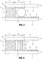
- a first substrate strip 30 having a first surface wettability is located on the interior substrate surface 12 between the active organic material and the perimeter.
- the first substrate strip 30 is in contact with at least a portion of the edge 16, and extends a first substrate distance d1 from the edge 16 and can extend around the entire perimeter. However, it is not necessary that the first substrate strip extend all the way out to the edge 16 or extend around the entire perimeter.
- a second substrate strip 32 having a second surface wettability different from the first surface wettability is located on the interior substrate surface 12 between the active organic material and the first substrate strip 30 and in contact with the first substrate strip 30.
- the second substrate strip 32 extends a second substrate distance d2 from the first distance d1 from the edge 16.
- a cover (50) which is a protective cover, has an interior cover surface 52, an exterior cover surface 54, and an edge corresponding to the edge 16 of the substrate; the interior cover surface 52 faces the interior substrate surface 12.
- a first cover strip 80 having the first surface wettability is spaced from the first substrate strip 30 within the perimeter and is located on the interior cover surface 52.
- the first cover strip 80 extends a first cover distance d1 from the edge 16.
- a second cover strip 82 having the second surface wettability spaced from the second substrate strip 32 within and in contact with the first cover strip 80 is located on the interior cover surface 52.
- the second cover strip 82 extends a second cover distance d2 from the first cover distance d1 from the edge 16.
- a sealing member 40 that wets the first substrate and cover strips 30, 80 but not the second substrate and cover strips 32, 82 is located along the edge 16 and in contact with both the first substrate strip 30 and first cover strip 80.
- the sealing member 40 extends a distance from the edge 16 less than or equal to the first substrate distance d1 and the first cover distance d1, adhered to the first substrate strip 30 and first cover strip 80 having the first surface wettability and not adhered to the second substrate strip 32 and second cover strip 82 having the second surface wettability.
- the width of the seal can be controlled by adjusting the distance d1.
- the distance d1 is chosen to be large enough that the sealing member 40 provides adequate sealing protection to the OLED device for the application intended.
- the sealing member material wets the first cover and first substrate strips 80, 30 and not the second cover and second substrate strips 82, 32.
- first cover and first substrate strips 80, 30 have an identical wettability
- second cover and second substrate strips 82, 32 have an identical wettability.
- the first substrate strip 30 be more wettable than the second substrate strip 32 and that the first cover strip 80 be more wettable than the second cover strip 82 by the material comprising the sealing member 40.
- the distance d1 on the cover 50 need not be identical to the distance d1 on the substrate 10 merely that both extend a distance from the edge 16 adequate to provide the desired moisture resistance and contact area for adhesion to the sealing member 40.
- the distance d2 on the cover 50 need not be identical to the distance d2 on the substrate 10, merely that the distance d2 on the cover 50 extend a distance on the cover 50 from the distance d1 on the cover 50 and distance d2 on the substrate 10 extend a distance on the substrate 10 from the distance d1 on the substrate 10 adequate to provide the desired moisture resistance.
- the distance d1 on the cover 50 is substantially the same as the distance d1 on the substrate 10 or the distance d2 on the cover 50 is substantially the same as the distance d2 on the substrate 10 or both.
- Electrode 22 and OLED material 20 are formed on the interior substrate surface 12 of the substrate 10.
- OLED devices are driven through electrodes that are conventionally electrically connected to a controller exterior to the OLED device.
- the electrodes 22 typically extend beyond the cover 50 on one side of the device, as shown in the top view of FIG. 2 and in the cross section of FIG. 6 .
- the edge 16 from which the first cover and substrate strips 30, 80 extend is defined as the edge of the cover rather than the corresponding substrate edge.
- the substrate 10 extends beyond the cover edge to provide an area 16' onto which the electrodes 22 extend and from which the electrodes 22 are externally accessible.
- an alternative sealing arrangement can be employed on the edge 16 at which the electrodes 22 are made externally accessible.
- an electrode insulation layer 34 can be employed between the sealing member 40 and the electrode 22 in the locations where the electrode 22 extends beneath the sealing member 40. As shown, the electrode 22 extends over the interior substrate surface 12 between the interior substrate surface 12 and the sealing member 40 and the electrode insulation layer 34 is located between the electrode 22 and the sealing member 40.
- first substrate strip 30 can be an uncoated portion of the substrate 10
- second substrate strip 32 can be an uncoated portion of the substrate 10
- first cover strip 80 can be an uncoated portion of the cover 50
- second cover strip 82 can be an uncoated portion of the cover 50.
- the first or second cover strips 80, 82 or first or second substrate strips 30, 32 are the surface of the substrate 10 or cover 50 itself. In such an embodiment, it is useful if the substrate 10, in particular, is insulating so that the electrodes 22 formed thereon conduct electricity along only the desired path.
- first or second cover strips 80, 82 or the first or second substrate strips 30, 32 are formed from a material different than the cover 50 or substrate 10 material ( FIG. 1 ).
- the metal can be coated with a non-conducting material having the desired wetting properties with respect to the sealing member 40.
- the sealing member 40 can be formed of a metal or metal alloy.
- Particularly useful metals include indium, tin, bismuth, lead, or solder, or alloys of these metals.
- a particularly useful alloy includes indium and tin in a ratio of 50:50, 52:48, 48:52, 55:45, or 45:55. These materials are useful in part because they have a relatively low melting temperature.
- OLED materials 20 for example organic temperature-sensitive materials coated on the interior substrate surface 12, can be damaged by heat and the use of low-melting-point metals reduces potential damage to the organic materials in the OLED.
- first and second cover strips 80, 82 and first and second substrate strips 30, 32 include metals, metal alloys, and metal oxides, for example copper, aluminum, silver, and aluminum oxide.
- Resins, for example photosensitive resins used in photo-lithography are also useful in providing differential wetting, particularly in combination with metal or metal alloy sealing materials.
- the first cover strip 80 and first substrate strip 30 have a glass surface
- the second cover strip 82 and second substrate strip 32 have an aluminum oxide surface
- the sealing member 40 is an alloy including tin and indium
- the first substrate strip 30 and the first cover strip 80 are formed from a material that is different than the material of the cover 50 or the substrate 10.
- the first cover strip 80 and first substrate strip 30 have a metal oxide surface
- the second cover strip 82 and second substrate strip 32 have a glass surface
- the sealing member 40 is a solder alloy.
- the first cover strip 80 and first substrate strip 30 have a silver surface
- the second cover strip 82 and second substrate strip 32 have an aluminum oxide surface
- the sealing member 40 is an alloy including tin and indium
- the first substrate strip 30 is an uncoated portion of the substrate 10 or wherein the first cover strip 80 is an uncoated portion of the cover 50.
- the requirement is that the sealing member 40 wets the first cover strip 80 and first substrate strip 30 and does not wet the second cover strip 82 and second substrate strip 32.
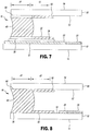
- adhesives and desiccants can also be provided between the interior substrate surface 12 and the interior cover surface 52 to complement the function of the sealing member 40.
- the adhesives 72 and desiccants 70 are located between the OLED material 20 and the sealing member 40 and adhere to both second cover strip 82 and second substrate strip 32.
- the adhesives 72 and desiccants 70 adhere to both the interior substrate surface 12 and the interior cover surface 52.
- the desiccant 70 usefully absorbs trapped moisture.
- the adhesive 72 is useful in providing a robust adhesion between the cover 50 and substrate 10 as the sealing member 40 may not necessarily provide adequate adhesion.
- the desiccants 70 and adhesives 72 can be layered to form one or more barriers as taught in the prior art.
- the adhesives 72 and desiccants 70 are located at the periphery of the OLED materials 20, while in a bottom emitter, desiccants can be located over the back of the OLED.
- spacer elements 60 shown in FIG. 3
- the spacer elements 60 may be located in the second cover and substrate strip areas or may be located farther toward the OLED material 20, for example above the electrodes 22.
- the sealing member 40 described above can be employed on one or all of the sides of the OLED device (as shown in FIG. 2 ). Hence, the entire perimeter of the cover 50 and substrate 10 can be sealed with the same sealing member 40.
- First and second substrate and cover strips 30, 32, 80, 82 having the first and second surface attributes, respectively, can be formed on the interior surfaces of the cover and substrate (52, 12) around the entire perimeter.
- the sealing member 40 can be employed on only a portion of the perimeter, as can the first and second cover strips 80, 82 and first and second substrate strips 30, 32.
- the sealing member 40 of the present invention can be constructed in a variety of ways.
- the first and second cover and substrate strips 80, 82, 30, 32 are first formed on the cover 50 and substrate 10, for example by sputtering or evaporating materials through a mask, by photolithographic methods, or by simply cleaning the surface of the cover 50 or substrate 10 when the surface is used as the strip.
- the cover 50 and substrate 10 are adhered in a desired, spaced-apart configuration, for example by employing the spacer elements 60 of FIG. 3 and an adhesive 72.
- the sealing member 40 can then be formed by dipping the substrate 10 and cover 50 together into molten sealing material, and removing the substrate and cover from the melted sealing material to thereby permit the sealing material to cool and harden.
- the sealing member 40 can be formed by depositing molten sealing material between the substrate 10 and cover 50 and then permitting the sealing material to cool and harden.
- the sealing member 40 can be formed by depositing sealing material between the substrate 10 and cover 50, heating the sealing material and then permitting the sealing material to cool and harden.
- the sealing material can be applied as a paste or applied as a dispersion, for example a dispersion of conductive nano-particles.
- the sealing material may be applied in a wire form and the sealing member 40 made by positioning a metal wire in the space between the first substrate strip 30 and first cover strip 80, melting the metal wire, and then cooling the melted material to form the sealing member 40. If the sealing material is not applied as a liquid, the sealing material is heated to form the sealing member 40 and adhere it to the wettable first cover and substrate strips to form a hermetic moisture barrier.
- Applicant has demonstrated the present invention by employing a glass cover and substrate adhered by a 1mm spacer.
- a mixture of 50% indium and 50% tin was melted at a temperature of 128 degrees C and applied between the glass cover and substrate without a coating on the interior glass surfaces (i.e. the first cover and substrate strips were glass) and shown to coat the glass surface.
- the edge was subsequently ground to form a polished, smooth, and hermetic seal between the substrate and cover.
- the use of a strip of aluminum oxide on a spaced-apart cover and substrate was demonstrated to repel the 50% mixture; that is the strips did not wet.
- a first strip was formed with evaporated aluminum on a cover and substrate, the cover and substrate were adhered in a spaced-apart configuration, and the 50% mixture applied as a molten metal.
- the cover, substrate, and sealing member were subsequently ground to form a hermetic barrier.
- molten commercial solders were shown not to wet glass but to wet metal layers, for example formed on glass.
- the 50% mixture was applied in solid form (for example as a wire) in the first strip area between the spaced-apart substrate and cover having the same strips as described above and subsequently heated with a hot metal surface.
- FIG. 5 illustrates the process with a local heat applicator 44 (e.g. a roller).
- the sealing member 40 then formed a barrier that was subsequently ground and shown to form a hermetic barrier. In this process, it is helpful if the heated surface does not wet the sealing member, to prevent the sealing member from adhering to the heating surface.
- a paste or a dispersion of metal particles can be applied as a solid or a liquid and dried (if necessary) between the spaced-apart substrate and cover in the first strip area. The paste or dispersion can be locally heated to melt the metal particles to form the sealing barrier.
- the metal particles are nano-particles having a lower melting temperature than larger metal particles.
- the present invention may be employed to provide a hermetic seal to an OLED device.
- the melting temperature of the 50% mixture 128 degrees C, is slightly less than the temperature at which the organic materials comprising the OLED device are damaged.
- the entire device was not heated, only the local periphery of the OLED device, so that the temperature of organic materials in an OLED device is not necessarily raised to the same temperature as the sealing member.
- the present invention can be employed in either top or bottom emitter configurations.
- Substrate 10 can be an organic solid, an inorganic solid, or a combination of organic and inorganic solids.
- Substrate 10 can be rigid or flexible and can be processed as separate individual pieces, such as sheets or wafers, or as a continuous roll.
- Typical substrate materials include glass, plastic, metal, ceramic, semiconductor, metal oxide, metal nitride, metal sulfide, semiconductor oxide, semiconductor nitride, semiconductor sulfide, carbon, or combinations thereof, or any other materials commonly used in the formation of OLED devices, which can be either passive-matrix devices or active-matrix devices.
- Substrate 10 can be a homogeneous mixture of materials, a composite of materials, or multiple layers of materials.
- Substrate 10 can be an OLED substrate that is a substrate commonly used for preparing OLED devices, e.g. active-matrix low-temperature polysilicon or amorphous-silicon TFT substrate.
- substrate 10 can comprise glass.
- the cover 50 can comprise the same or different materials as the substrate 10 and can have the same or different properties.
- Cover 50 can be an organic solid, an inorganic solid, or a combination of organic and inorganic solids.
- Cover 50 can be rigid or flexible, and can be processed as separate individual pieces, such as sheets or wafers, or as continuous rolls.
- Typical protective cover materials include glass, plastic, metal, ceramic, semiconductor, metal oxide, metal nitride, metal sulfide, semiconductor oxide, semiconductor nitride, semiconductor sulfide, carbon or combinations thereof.
- cover 50 can comprise glass.
- cover 50 can include one or more optically active layers for imparting desirable properties to an OLED device or to its emitted light.
- optically active layers include color filter arrays for limiting the wavelengths of emitted light, color change modules (e.g. fluorescent layers) for converting a range of wavelengths to another range of wavelengths, light-extraction layers for limiting losses due to total internal reflection, anti-reflection layers, and polarizing layers.
- a polymer buffer layer which can be any number of materials, including UV or heat cured epoxy resin, acrylates, or pressure sensitive adhesive, can be disposed between the substrate 10 and the cover 50.
- Typical moisture-absorbing desiccant materials include metals such as alkali metals (e.g. Li, Na), alkaline earth metals (e.g. Ba, Ca), or other moisture-reactive metals (e.g. Al, Fe); alkaline metal oxides (e.g. Li 2 O, Na 2 O); alkaline earth metal oxides (e.g. MgO, CaO, BaO); sulfates (e.g. anhydrous MgSO 4 ); metal halides (e.g. CaCl 2 ); perchlorates (e.g. Mg(ClO 4 ) 2 ); molecular sieves, especially molecular sieves treated at high temperature; organometallic compounds described by Takahashi et al.
- alkali metals e.g. Li, Na
- alkaline earth metals e.g. Ba, Ca
- sulfates e.g. anhydrous MgSO 4
- metal halides e.g. Ca
- Desiccant 70 can be a single material, a homogeneous mixture of materials, a composite of materials, or multiple layers of materials, and can be deposited from a vapor or from solution, or can be provided as particulate material or as particulate material formed in a porous matrix such as a permeable package or tape.
- Particularly useful desiccant materials include those that are particulate materials formed into a polymeric matrix that can be patterned, as described by Boroson et al. in U.S. Patent 6,226,890 .
- the desiccant materials can be expanding or non-expanding desiccants.
- an expanding desiccant we mean a desiccant that expands in volume upon absorbing moisture.
- expanding desiccants include reactive metals such as Li and oxides such as CaO. Such desiccants should not fill the entire space between the substrate and cover.
- non-expanding desiccants such as molecular sieves, is that they can fill the entire space.
- OLED devices that can be used in this invention have been well described in the art and OLED devices can include layers commonly used for such devices.
- a bottom electrode is formed over substrate 10 and is most commonly configured as an anode, although the practice of this invention is not limited to this configuration.
- Example conductors for this application include, but are not limited to, gold, iridium, molybdenum, palladium, platinum, aluminum or silver.
- Desired anode materials can be deposited by any suitable way such as evaporation, sputtering, chemical vapor deposition, or electrochemical processes.
- Anode materials can be patterned using well-known photolithographic processes.
- hole-transporting layer be formed and disposed over the anode.
- Desired hole-transporting materials can be deposited by any suitable method such as evaporation, sputtering, chemical vapor deposition, electrochemical processes, thermal transfer, or laser thermal transfer from a donor material.
- Hole-transporting materials useful in hole-transporting layers are well known to include compounds such as an aromatic tertiary amine, where the latter is understood to be a compound containing at least one trivalent nitrogen atom that is bonded only to carbon atoms, at least one of which is a member of an aromatic ring.
- the hole-transporting layer in an OLED device can be formed of a single or a mixture of aromatic tertiary amine compounds. Specifically, one can employ a triarylamine in combination with a tetraaryldiamine. When a triarylamine is employed in combination with a tetraaryldiamine, the latter is positioned as a layer interposed between the triarylamine and the electron-injecting and transporting layer.
- Another class of useful hole-transporting materials includes polycyclic aromatic compounds as described in EP 1 009 041 .
- polymeric hole-transporting materials can be used such as poly(N-vinylcarbazole) (PVK), polythiophenes, polypyrrole, polyaniline, and copolymers such as poly(3,4-ethylenedioxythiophene)/poly(4-styrenesulfonate), also called PEDOT/PSS.
- PVK poly(N-vinylcarbazole)
- polythiophenes polypyrrole
- polyaniline polyaniline
- copolymers such as poly(3,4-ethylenedioxythiophene)/poly(4-styrenesulfonate), also called PEDOT/PSS.
- Light-emitting layers produce light in response to hole-electron recombination.
- the light-emitting layers are commonly disposed over the hole-transporting layer.
- Desired organic light-emitting materials can be deposited by any suitable technique such as evaporation, sputtering, chemical vapor deposition, electrochemical processes, or radiation thermal transfer from a donor material. Useful organic light-emitting materials are well known.
- the light-emitting layers of the OLED element comprise a luminescent or fluorescent material where electroluminescence is produced as a result of electron-hole pair recombination in this region.
- the light-emitting layers can be comprised of a single material, but more commonly include a host material doped with a guest compound or dopant where light emission comes primarily from the dopant.
- the dopant is selected to produce color light having a particular spectrum.
- the host materials in the light-emitting layers can be an electron-transporting material, as defined below, a hole-transporting material, as defined above, or another material that supports hole-electron recombination.
- the dopant is usually chosen from highly fluorescent dyes, but phosphorescent compounds, e.g., transition metal complexes as described in WO 98/55561 , WO 00/18851 , WO 00/57676 , and WO 00/70655 are also useful.
- Dopants are typically coated as 0.01 to 10 % by weight into the host material.
- Host and emitting molecules known to be of use include, but are not limited to, those disclosed in U.S. Patents 4,768,292 ; 5,141,671 ; 5,150,006 ; 5,151,629 ; 5,294,870 ; 5,405,709 ; 5,484,922 ; 5,593,788 ; 5,645,948 ; 5,683,823 ; 5,755,999 ; 5,928,802 ; 5,935,720 ; 5,935,721 ; and 6,020,078 .
- the host material in the light-emitting layers can be an anthracene derivative having hydrocarbon or substituted hydrocarbon substituents at the 9 and 10 positions.
- derivatives of 9,10-di-(2-naphthyl)anthracene constitute one class of useful host materials capable of supporting electroluminescence, and are particularly suitable for light emission of wavelengths longer than 400 nm, e.g., blue, green, yellow, orange or red.
- Benzazole derivatives constitute another class of useful host materials capable of supporting electroluminescence, and are particularly suitable for light emission of wavelengths longer than 400 nm, e.g., blue, green, yellow, orange or red.
- An example of a useful benzazole is 2, 2', 2"-(1,3,5-phenylene)tris[1-phenyl-1H-benzimidazole].
- Desirable fluorescent dopants include perylene or derivatives of perylene, derivatives of anthracene, tetracene, xanthene, rubrene, coumarin, rhodamine, quinacridone, dicyanomethylenepyran compounds, thiopyran compounds, polymethine compounds, pyrilium and thiapyrilium compounds, derivatives of distryrylbenzene or distyrylbiphenyl, bis(azinyl)methane boron complex compounds, and carbostyryl compounds.
- organic emissive materials can be polymeric substances, e.g. polyphenylenevinylene derivatives, dialkoxy-polyphenylenevinylenes, poly-para-phenylene derivatives, and polyfluorene derivatives, as taught by Wolk et al. in commonly assigned U.S. Patent 6,194,119 B1 and references cited therein.
- Desired electron-transporting materials can be deposited by any suitable method such as evaporation, sputtering, chemical vapor deposition, electrochemical processes, thermal transfer, or laser thermal transfer from a donor material.
- Preferred electron-transporting materials for use in the electron-transporting layer are metal chelated oxinoid compounds, including chelates of oxine itself (also commonly referred to as 8-quinolinol or 8-hydroxyquinoline). Such compounds help to inject and transport electrons and exhibit both high levels of performance and are readily fabricated in the form of thin films.
- Exemplary of contemplated oxinoid compounds are those satisfying structural Formula E, previously described in U.S. 7,288,330 B2 .
- electron-transporting materials include various butadiene derivatives as disclosed in U.S. Patent 4,356,429 and various heterocyclic optical brighteners as described in U.S. Patent 4,539,507 . Certain benzazoles are also useful electron-transporting materials.
- Other electron-transporting materials can be polymeric substances, e.g. polyphenylenevinylene derivatives, poly-para-phenylene derivatives, polyfluorene derivatives, polythiophenes, polyacetylenes, and other conductive polymeric organic materials known in the art.
- An upper electrode most commonly configured as a cathode is formed over the electron-transporting layer, or over the light-emitting layers if an electron-transporting layer is not used. If the device is top-emitting, the electrode must be transparent or nearly transparent. For such applications, metals must be thin (preferably less than 25 nm) or one must use transparent conductive oxides (e.g. indium-tin oxide, indium-zinc oxide), or a combination of these materials. Optically transparent cathodes have been described in more detail in U.S. Patent 5,776,623 . Cathode materials can be deposited by evaporation, sputtering, or chemical vapor deposition.
- patterning can be achieved through many well known methods including, but not limited to, through-mask deposition, integral shadow masking as described in U.S. Patent 5,276,380 and EP 0 732 868 , laser ablation, and selective chemical vapor deposition.
- An OLED device can include other layers as well.
- a hole-injecting layer can be formed over the anode, as described in U.S. 4,720,432 , U.S. 6,208,075 , EP 0 891 121 A1 , and EP 1 029 909 A1 .
- An electron-injecting layer such as alkaline or alkaline earth metals, alkali halide salts, or alkaline or alkaline earth metal-doped organic layers, can also be present between the cathode and the electron-transporting layer.
Landscapes
- Physics & Mathematics (AREA)
- Condensed Matter Physics & Semiconductors (AREA)
- General Physics & Mathematics (AREA)
- Engineering & Computer Science (AREA)
- Computer Hardware Design (AREA)
- Microelectronics & Electronic Packaging (AREA)
- Power Engineering (AREA)
- Optics & Photonics (AREA)
- Electroluminescent Light Sources (AREA)
- Devices For Indicating Variable Information By Combining Individual Elements (AREA)
Applications Claiming Priority (2)
| Application Number | Priority Date | Filing Date | Title |
|---|---|---|---|
| US12/397,418 US7948178B2 (en) | 2009-03-04 | 2009-03-04 | Hermetic seal |
| PCT/US2010/025364 WO2010101763A1 (en) | 2009-03-04 | 2010-02-25 | Hermetic seal for an electronic device comprising an active organic material |
Publications (2)
| Publication Number | Publication Date |
|---|---|
| EP2404319A1 EP2404319A1 (en) | 2012-01-11 |
| EP2404319B1 true EP2404319B1 (en) | 2019-06-19 |
Family
ID=42060448
Family Applications (1)
| Application Number | Title | Priority Date | Filing Date |
|---|---|---|---|
| EP10706866.0A Active EP2404319B1 (en) | 2009-03-04 | 2010-02-25 | Hermetic seal for an electronic device comprising an active organic material |
Country Status (7)
Families Citing this family (19)
| Publication number | Priority date | Publication date | Assignee | Title |
|---|---|---|---|---|
| KR20110064670A (ko) * | 2009-12-08 | 2011-06-15 | 삼성모바일디스플레이주식회사 | 게터 조성물 및 상기 게터 조성물을 포함하는 유기 발광 장치 |
| WO2011108020A1 (ja) * | 2010-03-01 | 2011-09-09 | パナソニック株式会社 | 有機el装置およびその製造方法 |
| KR101127595B1 (ko) * | 2010-05-04 | 2012-03-23 | 삼성모바일디스플레이주식회사 | 유기 발광 표시 장치 및 그 제조방법 |
| KR20130065219A (ko) * | 2011-12-09 | 2013-06-19 | 삼성디스플레이 주식회사 | 유기 발광 표시 장치 및 그 제조 방법 |
| US9386714B2 (en) * | 2012-12-05 | 2016-07-05 | Nokia Technologies Oy | Apparatus for housing an electronic component, a method |
| CN103383992B (zh) * | 2013-08-13 | 2015-12-02 | 深圳市华星光电技术有限公司 | Oled器件的封装方法及用该方法封装的oled器件 |
| DE102013110174B4 (de) * | 2013-09-16 | 2025-04-10 | Pictiva Displays International Limited | Elektronisches Bauelement und Verfahren zur Herstellung eines elektronischen Bauelements |
| CN103531718B (zh) * | 2013-10-25 | 2015-12-09 | 上海大学 | Oled封装结构 |
| US9334154B2 (en) | 2014-08-11 | 2016-05-10 | Raytheon Company | Hermetically sealed package having stress reducing layer |
| KR101931010B1 (ko) * | 2014-08-11 | 2018-12-19 | 레이던 컴퍼니 | 응력 감소층을 갖는 기밀 밀봉된 패키지 |
| JP2018084764A (ja) * | 2016-11-25 | 2018-05-31 | 株式会社ブイ・テクノロジー | フレキシブル表示装置及びフレキシブル表示装置の封止方法 |
| US11551028B2 (en) | 2017-04-04 | 2023-01-10 | Hailo Technologies Ltd. | Structured weight based sparsity in an artificial neural network |
| US11544545B2 (en) | 2017-04-04 | 2023-01-03 | Hailo Technologies Ltd. | Structured activation based sparsity in an artificial neural network |
| US11615297B2 (en) | 2017-04-04 | 2023-03-28 | Hailo Technologies Ltd. | Structured weight based sparsity in an artificial neural network compiler |
| US11238334B2 (en) | 2017-04-04 | 2022-02-01 | Hailo Technologies Ltd. | System and method of input alignment for efficient vector operations in an artificial neural network |
| US10387298B2 (en) | 2017-04-04 | 2019-08-20 | Hailo Technologies Ltd | Artificial neural network incorporating emphasis and focus techniques |
| CN110429206B (zh) * | 2019-08-07 | 2021-11-23 | 京东方科技集团股份有限公司 | 封装盖板、显示装置、显示面板及显示面板的封装方法 |
| KR20220000440A (ko) * | 2020-06-25 | 2022-01-04 | 삼성디스플레이 주식회사 | 표시 장치 및 표시 장치의 제조 방법 |
| US11591879B2 (en) * | 2021-01-29 | 2023-02-28 | Halliburton Energy Services, Inc. | Thermoplastic with swellable metal for enhanced seal |
Family Cites Families (18)
| Publication number | Priority date | Publication date | Assignee | Title |
|---|---|---|---|---|
| US4885211A (en) | 1987-02-11 | 1989-12-05 | Eastman Kodak Company | Electroluminescent device with improved cathode |
| US4769292A (en) | 1987-03-02 | 1988-09-06 | Eastman Kodak Company | Electroluminescent device with modified thin film luminescent zone |
| JPH09148066A (ja) | 1995-11-24 | 1997-06-06 | Pioneer Electron Corp | 有機el素子 |
| WO2000008899A1 (en) | 1998-08-03 | 2000-02-17 | Uniax Corporation | Encapsulation of polymer-based solid state devices with inorganic materials |
| US6226890B1 (en) | 2000-04-07 | 2001-05-08 | Eastman Kodak Company | Desiccation of moisture-sensitive electronic devices |
| US6614057B2 (en) | 2001-02-07 | 2003-09-02 | Universal Display Corporation | Sealed organic optoelectronic structures |
| US6589675B2 (en) | 2001-11-13 | 2003-07-08 | Kuan-Chang Peng | Organic electro-luminescence device |
| TW515062B (en) | 2001-12-28 | 2002-12-21 | Delta Optoelectronics Inc | Package structure with multiple glue layers |
| KR100819864B1 (ko) | 2001-12-28 | 2008-04-07 | 엘지.필립스 엘시디 주식회사 | 유기전기발광소자 |
| US7202602B2 (en) | 2003-04-08 | 2007-04-10 | Organic Lighting Technologies Llc | Metal seal packaging for organic light emitting diode device |
| JP2005251407A (ja) | 2004-03-01 | 2005-09-15 | Sanyo Electric Co Ltd | 表示パネルの製造方法および表示パネル |
| EP1571704A1 (en) | 2004-03-04 | 2005-09-07 | Interuniversitair Microelektronica Centrum Vzw | Method for depositing a solder material on a substrate in the form of a predetermined pattern |
| US8405193B2 (en) * | 2004-04-02 | 2013-03-26 | General Electric Company | Organic electronic packages having hermetically sealed edges and methods of manufacturing such packages |
| JP4864728B2 (ja) | 2005-01-21 | 2012-02-01 | シチズンホールディングス株式会社 | 封着板およびその製造方法 |
| US7842891B2 (en) | 2005-01-21 | 2010-11-30 | Citizen Holdings Co. Ltd. | Sealing board and method for producing the same |
| US20070172971A1 (en) * | 2006-01-20 | 2007-07-26 | Eastman Kodak Company | Desiccant sealing arrangement for OLED devices |
| KR100688795B1 (ko) * | 2006-01-25 | 2007-03-02 | 삼성에스디아이 주식회사 | 유기전계발광 표시장치 및 그 제조방법 |
| JP5018820B2 (ja) * | 2009-04-03 | 2012-09-05 | 株式会社デンソー | El表示装置およびその製造方法 |
-
2009
- 2009-03-04 US US12/397,418 patent/US7948178B2/en active Active
-
2010
- 2010-02-25 CN CN201080019404.5A patent/CN102414812B/zh active Active
- 2010-02-25 WO PCT/US2010/025364 patent/WO2010101763A1/en active Application Filing
- 2010-02-25 EP EP10706866.0A patent/EP2404319B1/en active Active
- 2010-02-25 KR KR1020117023074A patent/KR101278251B1/ko active Active
- 2010-02-25 JP JP2011552990A patent/JP5165800B2/ja active Active
- 2010-03-02 TW TW099106028A patent/TWI397644B/zh active
Non-Patent Citations (1)
| Title |
|---|
| None * |
Also Published As
| Publication number | Publication date |
|---|---|
| CN102414812B (zh) | 2015-04-22 |
| TW201040416A (en) | 2010-11-16 |
| WO2010101763A1 (en) | 2010-09-10 |
| US20100225231A1 (en) | 2010-09-09 |
| TWI397644B (zh) | 2013-06-01 |
| KR101278251B1 (ko) | 2013-06-24 |
| KR20110134891A (ko) | 2011-12-15 |
| CN102414812A (zh) | 2012-04-11 |
| JP2012519938A (ja) | 2012-08-30 |
| JP5165800B2 (ja) | 2013-03-21 |
| US7948178B2 (en) | 2011-05-24 |
| EP2404319A1 (en) | 2012-01-11 |
Similar Documents
| Publication | Publication Date | Title |
|---|---|---|
| EP2404319B1 (en) | Hermetic seal for an electronic device comprising an active organic material | |
| US8016631B2 (en) | Desiccant sealing arrangement for OLED devices | |
| US20070172971A1 (en) | Desiccant sealing arrangement for OLED devices | |
| EP1299913B1 (en) | Method for making encapsulated organic electronic devices | |
| US8022624B2 (en) | Moisture protection for OLED display | |
| US7224116B2 (en) | Encapsulation of active electronic devices | |
| US20060087230A1 (en) | Desiccant film in top-emitting OLED | |
| US7812531B2 (en) | Preventing stress transfer in OLED display components | |
| US20060059705A1 (en) | Lewis acid organometallic desiccant | |
| KR101011718B1 (ko) | 유기 발광 소자 및 그 제조방법 | |
| KR100287863B1 (ko) | 유기전계발광소자 | |
| US20060060086A1 (en) | Desiccant having a reactive salt |
Legal Events
| Date | Code | Title | Description |
|---|---|---|---|
| PUAI | Public reference made under article 153(3) epc to a published international application that has entered the european phase |
Free format text: ORIGINAL CODE: 0009012 |
|
| 17P | Request for examination filed |
Effective date: 20110901 |
|
| AK | Designated contracting states |
Kind code of ref document: A1 Designated state(s): AT BE BG CH CY CZ DE DK EE ES FI FR GB GR HR HU IE IS IT LI LT LU LV MC MK MT NL NO PL PT RO SE SI SK SM TR |
|
| DAX | Request for extension of the european patent (deleted) | ||
| STAA | Information on the status of an ep patent application or granted ep patent |
Free format text: STATUS: EXAMINATION IS IN PROGRESS |
|
| 17Q | First examination report despatched |
Effective date: 20171107 |
|
| RAP1 | Party data changed (applicant data changed or rights of an application transferred) |
Owner name: GLOBAL OLED TECHNOLOGY LLC |
|
| GRAP | Despatch of communication of intention to grant a patent |
Free format text: ORIGINAL CODE: EPIDOSNIGR1 |
|
| STAA | Information on the status of an ep patent application or granted ep patent |
Free format text: STATUS: GRANT OF PATENT IS INTENDED |
|
| RIC1 | Information provided on ipc code assigned before grant |
Ipc: H01L 23/10 20060101AFI20181205BHEP Ipc: H01L 51/52 20060101ALI20181205BHEP |
|
| INTG | Intention to grant announced |
Effective date: 20190107 |
|
| GRAS | Grant fee paid |
Free format text: ORIGINAL CODE: EPIDOSNIGR3 |
|
| GRAA | (expected) grant |
Free format text: ORIGINAL CODE: 0009210 |
|
| STAA | Information on the status of an ep patent application or granted ep patent |
Free format text: STATUS: THE PATENT HAS BEEN GRANTED |
|
| AK | Designated contracting states |
Kind code of ref document: B1 Designated state(s): AT BE BG CH CY CZ DE DK EE ES FI FR GB GR HR HU IE IS IT LI LT LU LV MC MK MT NL NO PL PT RO SE SI SK SM TR |
|
| REG | Reference to a national code |
Ref country code: GB Ref legal event code: FG4D |
|
| REG | Reference to a national code |
Ref country code: CH Ref legal event code: EP |
|
| REG | Reference to a national code |
Ref country code: IE Ref legal event code: FG4D |
|
| REG | Reference to a national code |
Ref country code: DE Ref legal event code: R096 Ref document number: 602010059524 Country of ref document: DE |
|
| REG | Reference to a national code |
Ref country code: AT Ref legal event code: REF Ref document number: 1146576 Country of ref document: AT Kind code of ref document: T Effective date: 20190715 |
|
| REG | Reference to a national code |
Ref country code: NL Ref legal event code: MP Effective date: 20190619 |
|
| PG25 | Lapsed in a contracting state [announced via postgrant information from national office to epo] |
Ref country code: SE Free format text: LAPSE BECAUSE OF FAILURE TO SUBMIT A TRANSLATION OF THE DESCRIPTION OR TO PAY THE FEE WITHIN THE PRESCRIBED TIME-LIMIT Effective date: 20190619 Ref country code: FI Free format text: LAPSE BECAUSE OF FAILURE TO SUBMIT A TRANSLATION OF THE DESCRIPTION OR TO PAY THE FEE WITHIN THE PRESCRIBED TIME-LIMIT Effective date: 20190619 Ref country code: NO Free format text: LAPSE BECAUSE OF FAILURE TO SUBMIT A TRANSLATION OF THE DESCRIPTION OR TO PAY THE FEE WITHIN THE PRESCRIBED TIME-LIMIT Effective date: 20190919 Ref country code: HR Free format text: LAPSE BECAUSE OF FAILURE TO SUBMIT A TRANSLATION OF THE DESCRIPTION OR TO PAY THE FEE WITHIN THE PRESCRIBED TIME-LIMIT Effective date: 20190619 Ref country code: LT Free format text: LAPSE BECAUSE OF FAILURE TO SUBMIT A TRANSLATION OF THE DESCRIPTION OR TO PAY THE FEE WITHIN THE PRESCRIBED TIME-LIMIT Effective date: 20190619 |
|
| REG | Reference to a national code |
Ref country code: LT Ref legal event code: MG4D |
|
| PG25 | Lapsed in a contracting state [announced via postgrant information from national office to epo] |
Ref country code: BG Free format text: LAPSE BECAUSE OF FAILURE TO SUBMIT A TRANSLATION OF THE DESCRIPTION OR TO PAY THE FEE WITHIN THE PRESCRIBED TIME-LIMIT Effective date: 20190919 Ref country code: GR Free format text: LAPSE BECAUSE OF FAILURE TO SUBMIT A TRANSLATION OF THE DESCRIPTION OR TO PAY THE FEE WITHIN THE PRESCRIBED TIME-LIMIT Effective date: 20190920 Ref country code: LV Free format text: LAPSE BECAUSE OF FAILURE TO SUBMIT A TRANSLATION OF THE DESCRIPTION OR TO PAY THE FEE WITHIN THE PRESCRIBED TIME-LIMIT Effective date: 20190619 |
|
| REG | Reference to a national code |
Ref country code: AT Ref legal event code: MK05 Ref document number: 1146576 Country of ref document: AT Kind code of ref document: T Effective date: 20190619 |
|
| PG25 | Lapsed in a contracting state [announced via postgrant information from national office to epo] |
Ref country code: NL Free format text: LAPSE BECAUSE OF FAILURE TO SUBMIT A TRANSLATION OF THE DESCRIPTION OR TO PAY THE FEE WITHIN THE PRESCRIBED TIME-LIMIT Effective date: 20190619 Ref country code: PT Free format text: LAPSE BECAUSE OF FAILURE TO SUBMIT A TRANSLATION OF THE DESCRIPTION OR TO PAY THE FEE WITHIN THE PRESCRIBED TIME-LIMIT Effective date: 20191021 Ref country code: AT Free format text: LAPSE BECAUSE OF FAILURE TO SUBMIT A TRANSLATION OF THE DESCRIPTION OR TO PAY THE FEE WITHIN THE PRESCRIBED TIME-LIMIT Effective date: 20190619 Ref country code: EE Free format text: LAPSE BECAUSE OF FAILURE TO SUBMIT A TRANSLATION OF THE DESCRIPTION OR TO PAY THE FEE WITHIN THE PRESCRIBED TIME-LIMIT Effective date: 20190619 Ref country code: RO Free format text: LAPSE BECAUSE OF FAILURE TO SUBMIT A TRANSLATION OF THE DESCRIPTION OR TO PAY THE FEE WITHIN THE PRESCRIBED TIME-LIMIT Effective date: 20190619 Ref country code: SK Free format text: LAPSE BECAUSE OF FAILURE TO SUBMIT A TRANSLATION OF THE DESCRIPTION OR TO PAY THE FEE WITHIN THE PRESCRIBED TIME-LIMIT Effective date: 20190619 Ref country code: CZ Free format text: LAPSE BECAUSE OF FAILURE TO SUBMIT A TRANSLATION OF THE DESCRIPTION OR TO PAY THE FEE WITHIN THE PRESCRIBED TIME-LIMIT Effective date: 20190619 |
|
| PG25 | Lapsed in a contracting state [announced via postgrant information from national office to epo] |
Ref country code: IS Free format text: LAPSE BECAUSE OF FAILURE TO SUBMIT A TRANSLATION OF THE DESCRIPTION OR TO PAY THE FEE WITHIN THE PRESCRIBED TIME-LIMIT Effective date: 20191019 Ref country code: SM Free format text: LAPSE BECAUSE OF FAILURE TO SUBMIT A TRANSLATION OF THE DESCRIPTION OR TO PAY THE FEE WITHIN THE PRESCRIBED TIME-LIMIT Effective date: 20190619 Ref country code: IT Free format text: LAPSE BECAUSE OF FAILURE TO SUBMIT A TRANSLATION OF THE DESCRIPTION OR TO PAY THE FEE WITHIN THE PRESCRIBED TIME-LIMIT Effective date: 20190619 Ref country code: ES Free format text: LAPSE BECAUSE OF FAILURE TO SUBMIT A TRANSLATION OF THE DESCRIPTION OR TO PAY THE FEE WITHIN THE PRESCRIBED TIME-LIMIT Effective date: 20190619 |
|
| PG25 | Lapsed in a contracting state [announced via postgrant information from national office to epo] |
Ref country code: TR Free format text: LAPSE BECAUSE OF FAILURE TO SUBMIT A TRANSLATION OF THE DESCRIPTION OR TO PAY THE FEE WITHIN THE PRESCRIBED TIME-LIMIT Effective date: 20190619 |
|
| PG25 | Lapsed in a contracting state [announced via postgrant information from national office to epo] |
Ref country code: DK Free format text: LAPSE BECAUSE OF FAILURE TO SUBMIT A TRANSLATION OF THE DESCRIPTION OR TO PAY THE FEE WITHIN THE PRESCRIBED TIME-LIMIT Effective date: 20190619 Ref country code: PL Free format text: LAPSE BECAUSE OF FAILURE TO SUBMIT A TRANSLATION OF THE DESCRIPTION OR TO PAY THE FEE WITHIN THE PRESCRIBED TIME-LIMIT Effective date: 20190619 |
|
| PG25 | Lapsed in a contracting state [announced via postgrant information from national office to epo] |
Ref country code: IS Free format text: LAPSE BECAUSE OF FAILURE TO SUBMIT A TRANSLATION OF THE DESCRIPTION OR TO PAY THE FEE WITHIN THE PRESCRIBED TIME-LIMIT Effective date: 20200224 |
|
| REG | Reference to a national code |
Ref country code: DE Ref legal event code: R097 Ref document number: 602010059524 Country of ref document: DE |
|
| PLBE | No opposition filed within time limit |
Free format text: ORIGINAL CODE: 0009261 |
|
| STAA | Information on the status of an ep patent application or granted ep patent |
Free format text: STATUS: NO OPPOSITION FILED WITHIN TIME LIMIT |
|
| PG2D | Information on lapse in contracting state deleted |
Ref country code: IS |
|
| 26N | No opposition filed |
Effective date: 20200603 |
|
| PG25 | Lapsed in a contracting state [announced via postgrant information from national office to epo] |
Ref country code: SI Free format text: LAPSE BECAUSE OF FAILURE TO SUBMIT A TRANSLATION OF THE DESCRIPTION OR TO PAY THE FEE WITHIN THE PRESCRIBED TIME-LIMIT Effective date: 20190619 |
|
| REG | Reference to a national code |
Ref country code: CH Ref legal event code: PL |
|
| REG | Reference to a national code |
Ref country code: BE Ref legal event code: MM Effective date: 20200229 |
|
| PG25 | Lapsed in a contracting state [announced via postgrant information from national office to epo] |
Ref country code: MC Free format text: LAPSE BECAUSE OF FAILURE TO SUBMIT A TRANSLATION OF THE DESCRIPTION OR TO PAY THE FEE WITHIN THE PRESCRIBED TIME-LIMIT Effective date: 20190619 Ref country code: LU Free format text: LAPSE BECAUSE OF NON-PAYMENT OF DUE FEES Effective date: 20200225 |
|
| PG25 | Lapsed in a contracting state [announced via postgrant information from national office to epo] |
Ref country code: CH Free format text: LAPSE BECAUSE OF NON-PAYMENT OF DUE FEES Effective date: 20200229 Ref country code: LI Free format text: LAPSE BECAUSE OF NON-PAYMENT OF DUE FEES Effective date: 20200229 |
|
| PG25 | Lapsed in a contracting state [announced via postgrant information from national office to epo] |
Ref country code: IE Free format text: LAPSE BECAUSE OF NON-PAYMENT OF DUE FEES Effective date: 20200225 |
|
| PG25 | Lapsed in a contracting state [announced via postgrant information from national office to epo] |
Ref country code: BE Free format text: LAPSE BECAUSE OF NON-PAYMENT OF DUE FEES Effective date: 20200229 |
|
| PG25 | Lapsed in a contracting state [announced via postgrant information from national office to epo] |
Ref country code: MT Free format text: LAPSE BECAUSE OF FAILURE TO SUBMIT A TRANSLATION OF THE DESCRIPTION OR TO PAY THE FEE WITHIN THE PRESCRIBED TIME-LIMIT Effective date: 20190619 Ref country code: CY Free format text: LAPSE BECAUSE OF FAILURE TO SUBMIT A TRANSLATION OF THE DESCRIPTION OR TO PAY THE FEE WITHIN THE PRESCRIBED TIME-LIMIT Effective date: 20190619 |
|
| PG25 | Lapsed in a contracting state [announced via postgrant information from national office to epo] |
Ref country code: MK Free format text: LAPSE BECAUSE OF FAILURE TO SUBMIT A TRANSLATION OF THE DESCRIPTION OR TO PAY THE FEE WITHIN THE PRESCRIBED TIME-LIMIT Effective date: 20190619 |
|
| PGFP | Annual fee paid to national office [announced via postgrant information from national office to epo] |
Ref country code: DE Payment date: 20250218 Year of fee payment: 16 |
|
| PGFP | Annual fee paid to national office [announced via postgrant information from national office to epo] |
Ref country code: FR Payment date: 20250221 Year of fee payment: 16 |
|
| PGFP | Annual fee paid to national office [announced via postgrant information from national office to epo] |
Ref country code: GB Payment date: 20250219 Year of fee payment: 16 |