EP2403025A1 - Light-emitting device - Google Patents
Light-emitting device Download PDFInfo
- Publication number
- EP2403025A1 EP2403025A1 EP10746194A EP10746194A EP2403025A1 EP 2403025 A1 EP2403025 A1 EP 2403025A1 EP 10746194 A EP10746194 A EP 10746194A EP 10746194 A EP10746194 A EP 10746194A EP 2403025 A1 EP2403025 A1 EP 2403025A1
- Authority
- EP
- European Patent Office
- Prior art keywords
- layer
- nitride semiconductor
- semiconductor layer
- refractive index
- conductive film
- Prior art date
- Legal status (The legal status is an assumption and is not a legal conclusion. Google has not performed a legal analysis and makes no representation as to the accuracy of the status listed.)
- Withdrawn
Links
Images


Classifications
-
- H—ELECTRICITY
- H10—SEMICONDUCTOR DEVICES; ELECTRIC SOLID-STATE DEVICES NOT OTHERWISE PROVIDED FOR
- H10H—INORGANIC LIGHT-EMITTING SEMICONDUCTOR DEVICES HAVING POTENTIAL BARRIERS
- H10H20/00—Individual inorganic light-emitting semiconductor devices having potential barriers, e.g. light-emitting diodes [LED]
- H10H20/80—Constructional details
- H10H20/83—Electrodes
- H10H20/831—Electrodes characterised by their shape
- H10H20/8316—Multi-layer electrodes comprising at least one discontinuous layer
-
- H—ELECTRICITY
- H10—SEMICONDUCTOR DEVICES; ELECTRIC SOLID-STATE DEVICES NOT OTHERWISE PROVIDED FOR
- H10H—INORGANIC LIGHT-EMITTING SEMICONDUCTOR DEVICES HAVING POTENTIAL BARRIERS
- H10H20/00—Individual inorganic light-emitting semiconductor devices having potential barriers, e.g. light-emitting diodes [LED]
- H10H20/80—Constructional details
- H10H20/81—Bodies
- H10H20/814—Bodies having reflecting means, e.g. semiconductor Bragg reflectors
-
- H—ELECTRICITY
- H10—SEMICONDUCTOR DEVICES; ELECTRIC SOLID-STATE DEVICES NOT OTHERWISE PROVIDED FOR
- H10H—INORGANIC LIGHT-EMITTING SEMICONDUCTOR DEVICES HAVING POTENTIAL BARRIERS
- H10H20/00—Individual inorganic light-emitting semiconductor devices having potential barriers, e.g. light-emitting diodes [LED]
- H10H20/80—Constructional details
- H10H20/81—Bodies
- H10H20/819—Bodies characterised by their shape, e.g. curved or truncated substrates
- H10H20/82—Roughened surfaces, e.g. at the interface between epitaxial layers
-
- H—ELECTRICITY
- H10—SEMICONDUCTOR DEVICES; ELECTRIC SOLID-STATE DEVICES NOT OTHERWISE PROVIDED FOR
- H10H—INORGANIC LIGHT-EMITTING SEMICONDUCTOR DEVICES HAVING POTENTIAL BARRIERS
- H10H20/00—Individual inorganic light-emitting semiconductor devices having potential barriers, e.g. light-emitting diodes [LED]
- H10H20/80—Constructional details
- H10H20/81—Bodies
- H10H20/822—Materials of the light-emitting regions
- H10H20/824—Materials of the light-emitting regions comprising only Group III-V materials, e.g. GaP
- H10H20/825—Materials of the light-emitting regions comprising only Group III-V materials, e.g. GaP containing nitrogen, e.g. GaN
-
- H—ELECTRICITY
- H10—SEMICONDUCTOR DEVICES; ELECTRIC SOLID-STATE DEVICES NOT OTHERWISE PROVIDED FOR
- H10H—INORGANIC LIGHT-EMITTING SEMICONDUCTOR DEVICES HAVING POTENTIAL BARRIERS
- H10H20/00—Individual inorganic light-emitting semiconductor devices having potential barriers, e.g. light-emitting diodes [LED]
- H10H20/80—Constructional details
- H10H20/83—Electrodes
- H10H20/832—Electrodes characterised by their material
- H10H20/835—Reflective materials
-
- H—ELECTRICITY
- H10—SEMICONDUCTOR DEVICES; ELECTRIC SOLID-STATE DEVICES NOT OTHERWISE PROVIDED FOR
- H10H—INORGANIC LIGHT-EMITTING SEMICONDUCTOR DEVICES HAVING POTENTIAL BARRIERS
- H10H20/00—Individual inorganic light-emitting semiconductor devices having potential barriers, e.g. light-emitting diodes [LED]
- H10H20/80—Constructional details
- H10H20/85—Packages
- H10H20/857—Interconnections, e.g. lead-frames, bond wires or solder balls
-
- H—ELECTRICITY
- H10—SEMICONDUCTOR DEVICES; ELECTRIC SOLID-STATE DEVICES NOT OTHERWISE PROVIDED FOR
- H10H—INORGANIC LIGHT-EMITTING SEMICONDUCTOR DEVICES HAVING POTENTIAL BARRIERS
- H10H20/00—Individual inorganic light-emitting semiconductor devices having potential barriers, e.g. light-emitting diodes [LED]
- H10H20/80—Constructional details
- H10H20/84—Coatings, e.g. passivation layers or antireflective coatings
-
- H—ELECTRICITY
- H10—SEMICONDUCTOR DEVICES; ELECTRIC SOLID-STATE DEVICES NOT OTHERWISE PROVIDED FOR
- H10H—INORGANIC LIGHT-EMITTING SEMICONDUCTOR DEVICES HAVING POTENTIAL BARRIERS
- H10H20/00—Individual inorganic light-emitting semiconductor devices having potential barriers, e.g. light-emitting diodes [LED]
- H10H20/80—Constructional details
- H10H20/85—Packages
- H10H20/858—Means for heat extraction or cooling
- H10H20/8585—Means for heat extraction or cooling being an interconnection
Definitions
- This invention relates light emitting devices which comprises an LED chip (light emission diode chip). Particularly, this invention relates to a light emitting device which comprises an anode electrode, a p-type nitride semiconductor layer, and a dielectric layer which is located between the anode electrode and the p-type nitride semiconductor layer. The dielectric layer is located in a predetermined region which is along a plane perpendicular to a thickness direction of the LED chip.
- the prior LED chip comprises a light emission layer, an anode electrode, and a cathode electrode.
- the light emission layer is made of nitride semiconductor material such as GaN, InGaN, AIGaN, and InAlGaN.
- the anode electrode is disposed on one surface in a thickness direction of the light emission layer, and the cathode electrode is disposed on the other surface in the thickness direction of the light emission layer.
- the LED chip is flip-chip mounted on the mounting substrate.
- the research of improving the light extraction efficiency of the LED chip is conducted.
- the research and development of the LED chip having a structure which is designed so as not to prevent the anode electrode from being absorbed by the anode electrode is conducted.
- the LED chip having a structure of preventing absorption of the light in the anode is researched and developed.
- the above mentioned LED chip is disclosed in patent literature 1 which is mentioned below.
- the patent literature 1 discloses the LED chip which has a structure shown in Fig. 3 .
- LED chip comprises a light transmissive substrate 1, an n-type nitride semiconductor layer 2, a nitride light emission layer 3, a p-type nitride semiconductor layer 3 ;
- the light transmissive substrate 1 is made of sapphire substrate;
- the n-type nitride semiconductor layer 2, the nitride light emission layer 3, and the p-type nitride semiconductor layer 4 are located on one side surface of the light transmissive substrate 1.
- the anode electrode 7 is opposite of the nitride light emission layer 3 from the p-type nitride semiconductor layer 4.
- the cathode electrode 8 is located on the same side of the n-type nitride semiconductor layer 2 as the nitride light emission layer 3.
- the LED chip comprises a first transparent conductive film 9a, a second transparent conductive film 9b, a plurality of low refractive index dielectric layers 10P, a light reflective conductive film 11, and a barrier metal layer 14.
- the first transparent conductive film 9a, the second transparent conductive film 9b, a plurality of the low refractive index dielectric layers 10P, the light reflective conductive film 11, and the barrier metal layer 14 are interposed between the p-type nitride semiconductor layer 3 and the anode electrode 7.
- the first transparent conductive film 9a is formed on the p-type nitride semiconductor layer 4.
- the second transparent conductive film 9b is formed on the first transparent conductive film 9a.
- the low refractive index dielectric layers 10P are made of material which has a refractive index which is lower than a refractive index of the p-type nitride semiconductor layer 4.
- the low refractive index dielectric layers 10P are partially stacked on the second transparent conductive film 9b.
- the low refractive index dielectric layers 10P are configured to reflect the light which is emitted from the nitride light emission layer 3.
- the light reflective conductive film 11 is shaped to cover the low refractive index dielectric layers 10P and the second transparent conductive film 9b.
- the light reflective conductive film 11 is configured to reflect the light which is emitted from the nitride light emission layer 3.
- the barrier metal layer 14 is formed on the light reflective conductive film 11. That is to say , the LED chip of Fig. 3 has a light extracting surface in one surface in the thickness direction of the nitride light emission layer 3, and a first surface which is opposite of the light extracting surface from the nitride light emission layer 3. In addition, the LED chip is provided at its first surface with the low refractive index dielectric layers 10P.
- the nitride light emission layer 3 is configured to emit the light toward both the light extracting surface and the anode electrode 7.
- the nitride light emission layer 3 emits the light toward the anode electrode 7, the light is reflected by the low refractive index dielectric layers 10P and the light reflective conductive film 11.
- the low refractive index dielectric layers 14P and the light reflective conductive film 11 are configured to reflect the light toward the light extracting surface.
- the arrowed line C shown in Fig. 3B discloses one example of a path of the light which is emitted from the nitride light emission layer 3, which is taken in the low refractive index dielectric layers 10P, and which is reflected by the low refractive index dielectric layers.
- the above mentioned first transparent conductive film 9a has a thickness of 2 nm to 10 nm.
- the first transparent conductive film 9a is made of material such as Ni, Pd, Pt, Cr, Mn, Ta, Cu, Fe, or alloy including at least one of them.
- the second transparent conductive film 9b is made of one of the materials selected from ITO, IZO, ZnO, In 2 O 3 SnO 2 Mg x Zn 1-xO (x ⁇ 0.5), amorphous AIGaN, GaN, SiON.
- the light reflective conductive film 11 is made of material such as Ag, Al, and Rh.
- the anode electrode 7 is made of metal material of Au.
- the barrier metal layer 14 is made of material of Ti.
- Each one of the low refractive index dielectric layers 10P which are mentioned above has a cross section which is perpendicular to the thickness direction of the LED chip; the cross section of the low refractive index dielectric layer 10P has a circular shape.
- each one of the low refractive index dielectric layers 10P is disposed on the second transparent conductive film 9b such that the low refractive index dielectric layers 10P are arranged in the two dimensional array. More specifically, each one of the low refractive index dielectric layers 10P is disposed on a lattice point of a square lattice along the plane which is perpendicular to the thickness direction of the LED chip. That is, Fig.
- the LED chip which comprises a plurality of the low refractive index dielectric layers 10P; the low refractive index dielectric layers 10P is arranged along the plane in parallel with the nitride light emission layer 3; each one of the low refractive index dielectric layers 10P has an arrangement which resembles the island to be isolated from each other.
- the low refractive index dielectric layers 10P comprise alternating layers of two kinds of the dielectric layers; the two kinds of the dielectric layers have electrical insulation properties and are different in the refractive index from each other, whereby each one of the low refractive index dielectric layer 10P has a periodic structure that the refractive index is periodically changed.
- the low refractive index dielectric layers 10P are made of material such as SiO 2 , ZrO 2 , TiO 2 , Al 2 O 3 , Si 3 N 4 , and AIN.
- Patent literature 1 Japanese patent application publication No. 2007-258276A
- the light emitting device comprising the mounting substrate and the LED chip AA which has a structure shown in Fig. 3 and which is flip chip mounted on the mounting substrate
- the nitride light emission layer 3 emits the light to the n-type nitride semiconductor layer 2
- the light exits from the light extracting surface through the light transmissive substrate 1.
- the nitride light emission layer emits the light toward the p-type nitride semiconductor layer 4
- the light is reflected by the reflection member which is realized by a plurality of the low refractive index dielectric layers 10P and the light reflective conductive film 11.
- LED chip shown in Fig. 3 comprises a plurality of the low refractive index dielectric layers 10P; a plurality of the low refractive index dielectric layers are isolated from each other to have the arrangement which resembles the island shape. Therefore, this configuration makes it possible to prevent the operation voltage from being increased due to the low refractive index dielectric layers 10P. As a result, this configuration makes it possible to prevent the increase of the operation voltage and also to improve the light extracting efficiency at the same time.
- the above mentioned light emitting device comprises a plurality of the low refractive index dielectric layers 10P which are arranged in the two dimensional array on the second transparent conductive film 9b such that a plurality of the low refractive index dielectric layers 10P have arrangement which resembles the islands which are isolated from each other. Therefore, the anode electrode 7 is provided at its one surface with a first region which is overlapped with the bumps. In addition to this, the low refractive index dielectric layers 10P are also disposed on the first region.
- the low refractive index dielectric layers 10P are made of dielectric material having low heat conductive properties, compared with Au and GaN. (SiO 2 has the heat conductive property of 0.55 W / mK.
- Au has the heat conductive property of 320 W / mK.
- GaN has the heat conductive property of 130 W / mK.
- the film which is in contact with the low refractive index dielectric layers 10P is such as the second transparent conductive film 9b and the light reflective conductive film 11 .
- This invention is achieved to solve the above problem.
- This invention has an object of producing the light emitting device which is improved its heat radiation property and its luminescent efficiency.
- this invention discloses the light emitting device which comprises an LED chip and a mounting substrate.
- the LED chip comprises an n-type nitride semiconductor layer, a nitride light emission layer, a p-type nitride semiconductor layer, an anode electrode, and a cathode electrode.
- the n-type nitride semiconductor layer has a first surface.
- the nitride light emission layer is formed on the first surface of the n-type nitride semiconductor layer.
- the p-type nitride semiconductor layer is formed on the nitride light emission layer.
- the anode electrode is located in a position opposite of the nitride light emission layer from the p-type nitride semiconductor layer.
- the cathode electrode is formed on the first surface of the n-type nitride semiconductor layer.
- the LED chip is mounted on the mounting substrate.
- the mounting substrate has a patterned conductor.
- the patterned conductor is connected to the cathode electrode through a bump, and is connected to the anode electrode through a bump.
- the LED chip comprises one or more dielectric layers which have an arrangement which resembles an island.
- the dielectric layer has a refractive index which is smaller than the refractive index of the p-type nitride semiconductor layer.
- the dielectric layer is located between the p-type nitride semiconductor and the anode electrode.
- the p-type nitride semiconductor layer has a first region which is overlapped with the bump. The dielectric layer is not overlapped with the first region.
- This configuration makes it possible to improve the light extracting efficiency of the LED chip.
- this configuration makes it possible to decrease the thermal resistance between the LED chip and the mounting substrate. Therefore, it is possible to improve the heat radiation property.
- the LED chip further comprises a transparent conductive film and a light reflective conductive film.
- the transparent conductive film is disposed between the p-type nitride semiconductor layer and the anode electrode.
- the transparent conductive film has a refractive index which is smaller than the refractive index of the p-type nitride semiconductor layer.
- the light reflective conductive film is formed between the light transmissive conductive film and the anode electrode.
- the one or more dielectric layers are partially formed on the transparent conductive film to have the arrangement which resembles the island. The dielectric layer is located between the transparent conductive film and the anode electrode.
- This configuration also makes it possible to improve the light extracting efficiency of the LED chip.
- this configuration makes it possible to decrease the thermal resistance between the LED chip and the mounting substrate. Therefore, it is possible to improve the heat radiation property.
- the first region is a plane which is perpendicular to the thickness direction of the p-type nitride semiconductor layer.
- the plane defined as the first region has a circular shape.
- the first region is overlapped with the bump in the thickness direction of the p-type nitride semiconductor layer.
- the first region is a plane which is perpendicular to the thickness direction of the p-type nitride semiconductor layer.
- the plane which is defined by the first region has a circular shape. Consequently, the first region has an outer circumference.
- the first region is overlapped with the bump in the thickness direction of the p-type nitride semiconductor layer such that the bump is locate within the outer circumference of the first region.
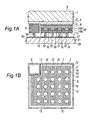
- the light emitting device shown in Fig. 1A the light emitting device comprises an LED chip A and a mounting substrate 20 which is configured to mount the LED chip A. It is noted that the upper-lower direction of Fig. 1A is equivalent to a thickness direction of the LED chip A, and also equivalent to a thickness direction of each one of the components of the LED chip A.
- the mounting substrate 20 comprises an electrical insulation substrate 21, a patterned conductor 27, and a patterned conductor 28.
- the electrical insulation substrate 21 has an electrical insulation property, is made of a substrate of aluminum nitride which has a high heat conductivity, and is shaped to have a plate shape.
- the patterned conductor 27 and the patterned conductor 28 are formed on one surface of the electrical insulation substrate 21.
- the patterned conductor 27 and the anode electrode 7 are joined together by the bump 37, and the patterned conductor 28 and the cathode electrode 8 are joined together by the bump 28.
- the mounting substrate 20 of this embodiment has a rectangular shape (square shape in this embodiment) in the planar view
- the shape of the mounting substrate 20 is not limited to the square shape; it is possible to employ the mounting substrate 20 to have a rectangular shape, a circular shape, and a hexagonal shape.
- the electrical insulation substrate 21 of the mounting substrate 20 also acts as the heat transfer plate which is configured to transfer the heat which is generated in the LED chip A.
- the electrical insulation substrate 21 may be exemplified by a glass epoxy substrate.
- the electrical insulation substrate 21 may be realized by the substrate having a heat conductivity which is higher than the heat conductivity of the substrate of the organic material. Therefore, the electrical insulation substrate 21 is not limited to the aluminum nitride substrate.
- the electrical insulation substrate 21 may be realized by the aluminum substrate, the porcelain enamel substrate, and the silicon substrate with the silicon dioxide film coat.
- the patterned conductors 27 and 28 are realized by the multilayered film which comprises a Cu film, Ni film, and Au film which is defined as a topmost layer.
- Each one of the bumps 37 and 38 is made of material of Au.
- the bumps 37 and 38 are, so called, a stud bump; the bumps 37 and 38 are formed on the surface of each one of the patterned conductor by way of stud bump method.
- the stud bump method is, in other words, the ball bump method.
- the number of the bump 37 has no limits. However, there is a need to efficiently release the heat in the LED chip A. Therefore, it is preferred to employ a large number of the bumps 27.
- the LED chip When the mounting of the LED chip A is performed, the LED chip is aligned to an accuracy of about plus or minus 5 micro meters, and receives the load by the ultrasonic sound wave.
- a diameter of the circular shaped joint area of the bump 37 with respect to the anode electrode 7 is smaller than the diameter of a circular shaped joint area of the bump 37 with respect to the patterned conductor 27.
- the diameter of the circular shaped joint area of the bump 38 with respect to the cathode electrode 8 is smaller than the diameter of the circular shaped joint area of the bump 38 with respect to the patterned conductor 28.
- the bumps 37 and the bumps 38 may be produced by means of the plating method.
- the above mentioned LED chip A comprises the light transmissive substrate 1 and the n-type nitride semiconductor layer 2;
- the light transmissive substrate 1 is made of GaN substrate to have one surface which correspondes to the lower surface of the light transmissive substrate 1 shown in Fig. 1A ;
- the n-type nitride semiconductor layer 2 which is realized by the n-type GaN layer is formed on the same side as the lower surface of the light transmissive substrate 1.
- n-type nitride semiconductor layer 2 has a lower surface which is equivalent to the first surface.
- the nitride light emission layer is formed on the lower surface of the n-type nitride semiconductor layer 2.
- the nitride light emission layer 3 has a quantum well structure.
- the p-type nitride semiconductor layer 4 which is realized by p-type GaN layer is formed on the nitride light emission layer 3.
- p-type nitride semiconductor layer 4 is opposite of the n-type nitride semiconductor layer 2 from the nitride semiconductor layer 4.
- the LED chip A comprises the light transmissive substrate 1 and a stacking structure;
- the stacking structure comprises the n-type nitride semiconductor layer 2, the nitride light emission layer 3, and the p-type nitride semiconductor layer 4 which are located on the same side as the one surface of the light transmissive substrate 1.
- the n-type nitride semiconductor layer 2, the nitride light emission layer 3, and the p-type nitride semiconductor layer 4 are formed on the on the one surface of the light transmissive substrate 1 by means of the epitaxial growth method such as MOVPE method. Therefore, it is possible to employ the buffer layer between the light transmissive substrate 1 and the n-type nitride semiconductor layer 2.
- the crystal growth method of the n-type nitride semiconductor layer 2, the nitride light emission layer 3, and the p-type nitride semiconductor layer 4 is not limited to the MOVPE method.
- the n-type nitride semiconductor layer 2, the nitride light emission layer 3, and the p-type nitride semiconductor layer 4 may be formed by means of the crystal growth method such as hydride vaper phase epitaxy method, and molecular beam epitaxial method.
- the light transmissive substrate 1 it is required for the light transmissive substrate 1 to have a transparency for passing the light which is emitted from the nitride light emission layer 3. That is, the light transmissive substrate 1 is exemplified by sapphire substrate, SiC substrate, and ZnO substrate.
- the anode electrode 7 is formed in a position opposite of the nitride light emission layer 3 from the p-type nitride semiconductor layer 4.
- the cathode electrode 8 is formed on the first surface of the n-type nitride semiconductor layer 2; the first surface is on the same side of the n-type nitride semiconductor layer 2 as the nitride light emission layer 3.
- the cathode electrode 8 is formed on the n-type nitride semiconductor layer 2 by way of the following steps.
- a first step is performed; in the first step, the n-type nitride semiconductor layer, the nitride light emission layer 3, and the p-type nitride semiconductor layer 4 are formed in order.
- the stacked film which comprises the n-type nitride semiconductor layer 2, the nitride light emission layer 3, and the p-type nitride semiconductor layer 4 is formed.
- the second step of etching a predetermined region of the stacked film is performed to etch the stacked film from the surface of the p-type nitride semiconductor layer 4 down to a mid portion of the n-type nitride semiconductor layer 2.
- the n-type nitride semiconductor layer 2 comprises the first area and the second area.
- the first area corresponds to the area where the nitride semiconductor layer is formed.
- the second area corresponds to the area where the cathode electrode 8 is formed. The second area is spaced from the first area.
- the holes are injected into the p-type nitride semiconductor layer 4.
- the electrons are injected into the n-type nitride semiconductor layer 2.
- the electrons and the holes are injected into the nitride light emission layer 2
- the electrons and the holes are recombined with each other in the nitride light emission layer 3. Consequently, the nitride light emission layer 2 emits the light.
- n-type nitride semiconductor layer 2 is realized by the n-type GaN layer which is formed on the light transmissive substrate 1.
- n-type nitride semiconductor layer 2 is not limited to the single layer structure. That is, the nitride semiconductor layer 2 may be realized by the multilayer structure.
- the light transmissive substrate 1 is realized by the sapphire substrate
- the multilayered n-type nitride semiconductor layer which comprises the buffer layer such as AIN layer and AlGaN layer on the one surface of the light transmissive substrate 1, the n-type AlGaN layer on the buffer layer, and the n-type GaN layer on the n-type GaN layer on the N-type AlGaN layer.
- the nitride light emission layer 3 has a quantum well structure which comprises the barrier layers and the well layer which is interposed between the barrier layers; the barrier layers are realized by the GaN layers, and the well layer is realized by the InGaN layer.
- the InGaN layer has a composition which is determined to emit the light having the emission peak wavelength of 450 nm.
- the emission wavelength (the emission peak wavelength) of the nitride light emission layer 3 is not limited thereto.
- the nitride light emission layer 3 is not limited to have a quantum well structure of single quantum well structure; it is possible to employ the nitride light emission layer 3 to have a quantum well structure of multiple quantum well structure.
- the nitride light emission layer having the quantum well structure there is no necessary to employ the nitride light emission layer having the quantum well structure; it is possible to employ the nitride light emission layer having a single layer structure.
- the nitride light emission layer 3 it is only required for the nitride light emission layer 3 to use the material of the nitride semiconductor material. Therefore, it is possible for the nitride light emission layer 3 to use the material such as AllnGaN, AlInN, and AlGaN in order to obtain a desired emission wavelength.
- the p-type nitride semiconductor layer 4 is realized by the p-type GaN layer which is formed on the nitride light emission layer 3.
- the p-type nitride semiconductor layer 4 is not limited to the single layer structure; it is possible to employ the p-type nitride semiconductor layer 4 having the multilayered structure.
- the p-type nitride semiconductor layer 4 having a first p-type semiconductor layer and a second p-type semiconductor layer the first p-type semiconductor layer may be realized by the p-type AlGaN layer, and the second p-type semiconductor layer may be realized by p-type GaN layer.
- the anode electrode 7 has a multilayered structure which comprises the first Au layer, the Ti layer, and the second Au layer; the first Au layer is disposed on the light reflective conductive film 11 which is explained below; the Ti layer is disposed on the first Au layer; the second Au layer is disposed on the Ti layer.
- the second Au layer which is located on the topmost of the multilayered structure is defined as the p-pad layer.
- the cathode electrode 8 has a multilayered structure which comprises a Ti layer on the n-type nitride semiconductor layer 2 and Au layer on the Ti layer.
- Au layer acts as the n-pad layer.
- the Ti layer on the n-type nitride semiconductor layer 2 is provided to act as the ohmic contact layer with respect to the n-type nitride semiconductor layer 2.
- the ohmic contact layer may employ its material such as Ti, V, Al and alloy which comprises at least one of them.
- the LED chip A further comprises a transparent conductive film 9, a light reflective conductive film 11, and low refractive index dielectric layers 10.
- the low refractive index dielectric layers 10 are, in other words, a dielectric layer.
- the transparent conductive film 9, the light reflective conductive film 11, and the low refractive index dielectric layers 10 are interposed between the p-type nitride semiconductor layer 4 and the anode electrode 7.
- the transparent conductive film 9 is disposed on one surface of the p-type nitride semiconductor layer.
- the transparent conductive film 9 is opposed of the nitride light emission layer 3 from the p-type nitride semiconductor layer.
- the transparent conductive film 9 is realized by the GZO (Ga doped ZnO) film which has a refractive index which is smaller than a refractive index of the p-type nitride semiconductor layer 6.
- the light reflective conductive film 11 is opposed of the p-type nitride semiconductor layer 2 from the transparent conductive film. Therefore, the light reflective conductive film 11 is interposed between the transparent conductive film 9 and the anode electrode.
- the light reflective conductive film 11 is realized by Ag film which has an electrical conductivity and a light reflectivity of reflecting the light which is emitted from the nitride light emission layer 3.
- the low refractive index dielectric layers 10 are interposed between the transparent conductive film 9 and the light reflective conductive film 11.
- the low refractive index dielectric layers 10 are disposed on the transparent conductive film 9 partially. Each one of the low refractive index dielectric layer 10 has a refractive index which is lower than the refractive index of the p-type nitride semiconductor layer 4.
- the low refractive index dielectric layers 10 have an arrangement which resembles the islands of being isolated from each other.
- the transparent conductive film 9 is realized by GZO which is formed to have a thickness of 10 nanometers.
- the transparent conductive film 9 is not limited its thickness thereto.
- this embodiment discloses the transparent conductive film 9 which is made of material of GZO.
- the transparent conductive film 9 is made of material which is selected from a group of GZO, AZO (Al doped ZnO), and ITO.
- the transparent conductive film 9 which is made of material which is selected from the above group makes it possible for the transparent conductive film 9 to establish the ohmic contact with respect to the p-type nitride semiconductor layer 6.
- the transparent conductive film 9 is formed by such as the GZO film, AZO film, and ITO film
- the transparent conductive film 9 is formed by the following steps. First, the film such as GZO film, AZO film, and ITO film are formed by way of the electron beam evaporation method with assistance of O 2 gas. Subsequently, GZO film, AZO film, and ITO film is annealed in a mixed gas of N 2 gas and O 2 gas. This step makes it possible to obtain the transparent conductive film 9 having the extinction coefficient of about 0.001. Following explains the anneal condition for forming the GZO film as the transparent conductive film 9.
- the transparent conductive film 9 is not limited its forming method and its forming condition to the above example. However, it is preferred to determine the forming method and the forming condition to form the transparent conductive film which has the extinction coefficient k of 0.003 or less.
- the transparent conductive film may be realized by, for example, a Pt film having a thickness of 0.1 nm. In addition, Pt film has a light transmissibility with regard to wavelength of 450 nm which becomes increases as the thickness of the Pt film decreases.
- the thickness of the Pt film is smaller than 0.6 nm, the light transmissibility of the Pt film decreases to about 95 %.
- the Pt film having the thickness of 0.6 nm has the light reflectivity which is approximately equal to the light reflectivity of the light reflective conductive film 11 made of Ag film. Therefore, it is preferred to employ the Pt film having 0.5 nm or less when the Pt film is employed as the transparent conductive film 9.
- the light reflective conductive film 11 is realized by the Ag film having a thickness of 100 nm.
- the light reflective conductive film 11 is not limited its thickness thereto. It is possible to employ the Ag film having a thickness of 50 nm to 200 nm.
- the light reflective conductive film 11 is not limited its material to Ag.
- the light reflective conductive film 11 may be made of the material such as Al. However, the light reflective conductive film 11 is preferred to be made of Ag, compared with Al.
- the light reflective conductive film 11 which is made of Ag has a high light reflectivity with respect to the light (ultraviolet light to visible light) emitted from the nitride light emission layer 3, compared with the light reflectivity of the light reflective conductive film which is made of Al.
- the low refractive index dielectric layer 10 comprises the SiO 2 layer 10a and a ZrO 2 layer 10b; the SiO 2 layer 10a is formed on the transparent conductive film 9; the ZrO 2 layer 10b is formed on the SiO 2 layer 10a. It is noted that the low refractive index dielectric layer 10 is only required to comprise at least one SiO 2 layer 10a and at least one ZrO 2 layer 10b. However, it is possible to employ the low refractive index dielectric layer 10 which is realized by the stacked layer which comprises the first SiO 2 layer, ZrO 2 layer, and the second SiO 2 layer.
- the low refractive index dielectric layer 10 may be realized by a single layer which is made of material which is selected from at least one of SiO 2 , ZrO 2 , Al 2 O 3 , and Y 2 O 3 .
- the above mentioned stacked films and the single film make it possible for the low refractive index dielectric layer 10 to have the extinction coefficient of approximately zero. Therefore, it is possible to prevent an absorption loss of the light in the low refractive index dielectric layer 10.
- SiO 2 has a refractive index of 1.46 and ZrO 2 has a refractive index of 1.97.
- Al 2 O 3 has the refractive index of 1.7 to 1.9.
- Y 2 O 3 has the refractive index of 1.8 to 2.0.
- the low refractive index dielectric layer 10 is not limited its material having the low refractive index, compared with the refractive index of the transparent conductive film 9.
- the low refractive index dielectric layer 10 may be made of material having the refractive index which is greater than the refractive index of the transparent conductive film 9.
- the material which satisfies the above requirement is exemplified by TiO 2 , CeO 2 , Nb 2 O 5 , and Ta 2 O 5 .
- the low refractive index dielectric layer 10 is preferred to be made of material of SiO 2 , ZrO 2 , Al 2 O 3 , and Y 2 O 3 each of which has a refractive index which is lower than the refractive index of TiO 2 , CeO 2 , Nb 2 O 5 , and Ta 2 O 5 .
- the low refractive index dielectric layer 10 being made of SiO 2 , ZrO 2 , Al 2 O 3 , and Y 2 O 3 has a light reflectivity which is higher than the light reflectivity of the low refractive index dielectric layer 10 being made of TiO 2 , CeO 2 , Nb 2 O 5 , and Ta 2 O 5 .
- the low refractive index dielectric layer 10 is made of material which is selected from one of the group of SiO 2 , ZrO 2 , Al 2 O 3 , Y 2 O 3 , TiO 2 , CeO 2 , Nb 2 O 5 , and Ta 2 O 5.
- the low refractive index dielectric layer 10 is designed to have its refractive index which is represented as "n”.
- the nitride light emission layer 3 is designed to emit the light having an emission wavelength of ⁇ (nm).
- a various kinds of the low refractive index dielectric layers 10 having the thickness equal to integral multiple of ⁇ /4n is used to perform the simulation for obtaining the incident angle dependence of the light reflectivity with respect to the low refractive index dielectric layer 10.
- the low refractive index dielectric layer 10 is set to have the thickness which is equal to or more than five-quarters of the emission wavelength of the light which is emitted from the nitride light emission layer 3, it was confirmed that decrease of the light reflectivity with respect to a predetermined incident angle caused by the evanescent light is inhibited.
- the low refractive index dielectric layer 10 satisfies the condition of having a thickness which is five-quarters or more greater than the optical wavelength ( ⁇ /n) of the emission wavelength of the nitride light emission layer 3, the improvement of the light extraction efficiency is confirmed.
- the low refractive index dielectric layer 10 is realized by the stacked film which comprises the SiO 2 layer 10a and the ZrO 2 layer 10b, it is desired to satisfy the following condition.
- the thickness of SiO 2 layer 10a is defined as "t1”.
- the refractive index of SiO 2 layer 10a is defined as "n1".
- the thickness of ZrO 2 layer 10b is defined as "t2".
- the refractive index of ZrO 2 is defined as "n2". Under these conditions, the formula of (t1 ⁇ ⁇ /4n1 + t2 ⁇ ⁇ /4n2) ⁇ (5/4) ⁇ is satisfied.
- the low refractive index dielectric layer 10 comprises the SiO 2 layer 10a to have a thickness t1 which is equal to 31.1 nm and the ZrO 2 layer 10b to have a thickness t2 which is equal to 159.1 nm such that the low refractive index dielectric layer 10 has an internal stress of zero.
- the low refractive index dielectric layer 10 may have a SiO 2 layer 10a and a ZrO 2 layer 10b each of which is designed to have an appropriate thickness, whereby it is possible to improve the reflectivity of the low refractive index dielectric layer. Further, when the low refractive index dielectric layer 10 is realized by the above explained stacked layer, it is possible to relax the internal stress of the low refractive index dielectric layer 10 by designing the thicknesses of the SiO 2 layer 10a and the ZrO 2 layer 10b, arbitrarily. As a result, it is possible to improve the adhesiveness between the low refractive index dielectric layer 10 and the transparent conductive film 9.
- LED chip A has a light transmissive substrate 1 which has a rectangular shape (a square shape) in the planar view.
- the LED chip A has the light transmissive substrate 1 to have a rectangular shape (square shape) along a direction perpendicular to the thickness direction of the LED chip A.
- the anode electrode 7 has a shape in the planar view of the rectangular shape (the square shape); the shape in the planar view of the anode electrode 7 is slightly smaller than the light transmissive substrate 1 to have at its one of the four corners with a cutout.
- the LED chip A has the anode electrode 7 which has the one surface along the direction perpendicular to the thickness direction of the LED chip A ; the one surface of the anode electrode 7 is slightly smaller than the light transmissive substrate 1.
- the anode electrode 7 has the four corners; one of the four corners is provided with the cutout.
- the cathode electrode 8 has a rectangular shape in the planar view to be located within the cutout of the anode electrode 7.
- the cathode electrode 8 has one surface along the plane perpendicular to the thickness direction of the LED chip A.
- the cathode electrode 8 has a dimension such that the cathode electrode is located within the cutout of the anode electrode.
- the anode electrode 7 has a dimension which is greater than the dimension of the cathode electrode.
- the anode electrode 7 has the one surface which is greater than the one surface of the cathode electrode. It is noted that the shape of each one of the anode electrode 7 and the cathode electrode 8 is not limited thereto.
- the LED chip A further comprises a plurality of the low refractive index dielectric layers 10 which has an arrangement which resembles an island of being isolated from each other; the low refractive index dielectric layers 10 are arranged on the transparent conductive film 9.
- Each one of the low refractive index dielectric layer 10 has an approximately circular shape in the planar view.
- the low refractive index dielectric layer 10 has a circular cross section which is perpendicular to the thickness direction of the LED chip. Therefore, in each one of the low refractive index dielectric layer 10, the low refractive index dielectric layer 10 has a center and an outer circumference which make an approximately constant distance from the center of the low refractive index dielectric layer 10.
- the light reflective conductive film 11 has a portion which surrounds an entire of the low refractive index dielectric layer 10. Consequently, it is possible to improve the uniformity of the electrical current density of the portion of the light reflective conductive film 11 which surrounds the entire of the low refractive index dielectric layer 10.
- the low refractive index dielectric layer 10 has the circular shape in the planar view.
- the regular polygon has equal to or more than six corners.
- this embodiment discloses the LED chip A which comprises a plurality of the low refractive index dielectric layers on the transparent conductive film 9; a plurality of the low refractive index dielectric layers 10 are arranged in two dimensional arrays.
- the low refractive index dielectric layers 10 have a plane area which is equal to or less than 70 percents of a plane area of the transparent conductive film 9.
- the low refractive index dielectric layer 10 has a circular shape, as explained in the above, in planar view, and has a diameter of 5 micrometers.
- the numerical value is only one example. Therefore, the numerical value is not limited to the above numerical value.
- this embodiment discloses the LED chip A which comprises the transparent conductive film 9.
- the anode electrode 7 has regions each of which is connected to the bump 37.
- the transparent conductive film 9 has first regions each of which is overlapped with the region of the bumps 37 which is connected to the anode electrode 7. Each one of the first regions is slightly greater than the region of the bump 37. Any one of the low refractive index dielectric layers 10 is not provided within each one of the first regions 12 so as not to be overlapped with the first region.
- the p-type nitride semiconductor layer 4 has a first region 12.
- the anode electrode 7 has regions each of which is connected to the bump 37.
- Each one of the first regions 12 of the p-type nitride semiconductor layer 4 is slightly greater than each one of the regions of bumps which are connected to the anode electrode 7.
- Each one of the low refractive index dielectric layers 10 is not provided within each one of the first regions 12 of the p-type nitride semiconductor layer 4.
- the transparent film 9 has a first region 12.
- the first region 12 of the transparent conductive film 9 is defined by the plane which is perpendicular to the thickness direction of the transparent conductive film.
- the first region 12 of the transparent conductive film 9 is defined by a plane which is perpendicular to the thickness direction of the p-type nitride semiconductor layer 4.
- the transparent conductive film 9 is formed on the p-type nitride semiconductor layer 4. Therefore, the p-type nitride semiconductor layer 4 also has the first region 12.
- the first regions 12 of the p-type nitride semiconductor layer 4 are defined by the planes which are perpendicular to the thickness direction of the p-type nitride semiconductor layer.
- Each one of the first region 12 of the transparent conductive film 9 is overlapped with the bump 37 in the thickness direction of the transparent conductive film.
- Each one of the first region 12 of the p-type nitride semiconductor layer 4 is overlapped with the bump 37 in the thickness direction of the p-type nitride semiconductor layer 4.
- Each one of the first region 12 has a dimension which is perpendicular to the thickness direction of the transparent conductive film 9; each one of the bump 37 has a dimension which is perpendicular to the thickness direction of the transparent conductive film 9; the dimension of the first region 12 is greater than the dimension of the bump 37.
- the LED chip A has the first regions 12 each of which has a circular shape in the planar view.
- Each one of the bumps 37 which is connected to the anode electrode 7 has a projection domain in the planar view; each of the projection domains is located within the first region 12.
- each one of the bumps 37 which is connected to the anode electrode 7 has the outer circumference; an entire of the outer circumference of each one of the bumps 37 is located in an inside of the outer circumference of the first region 12.
- each one of the first region 12 is only required to be overlapped with "the region of each one of the bumps 37" in the thickness direction of the transparent conductive film 9.
- the shape in the planar view of the first region 12 is defined by a portion which is surrounded by the low refractive index dielectric layers 10.
- each one of the bumps 37 which is connected to the anode electrode 7 is formed to have a diameter of 80 micrometers in the cross section.
- the first region 12 is formed to have a diameter of 100 micrometer.
- the numerical values of the above diameters are disclosed as an example. Therefore, the numerical values of the above diameters are not limited to the above numerical values.
- the light emitting device in this embodiment comprises the transparent conductive film 9, the light reflective conductive film 11, and a plurality of the low refractive index dielectric layers 10 which has an arrangement which resembles the islands to be isolated from each other.
- the LED chip A is shaped to have the transparent conductive film 9 which is interposed between the p-type nitride semiconductor layer 4 and the anode electrode 7.
- the transparent conductive film 9 is disposed in a position opposite of the nitride light emission layer 3 from the p-type nitride semiconductor layer 4.
- the transparent conductive film 9 has a refractive index which is smaller than the refractive index of the p-type nitride semiconductor layer 4.
- the light reflective conductive film 11 is located in a position opposite of the p-type nitride semiconductor layer 4 from the transparent conductive film 9.
- the light reflective conductive film 11 has the electrical conductivity, and is configured to reflect the light which is emitted from the nitride light emission layer 3.
- the low refractive index dielectric layers 10 are formed between the transparent conductive film 9 and the light reflective conductive film 11 to be located on the transparent conductive film 9, partially.
- the low refractive index dielectric layers 10 have the refractive index which is smaller than the refractive index of the p-type nitride semiconductor layer 4. With this configuration, it is possible to produce the LED chip A which has a high light extracting efficiency.
- the transparent conductive film 9 has the first regions 12.
- the first region is overlapped with each one of the bumps 37 in the thickness direction of the transparent conductive film. Any one of the low refractive index dielectric layers 10 are not formed in the first region 12 so as not to be overlapped with the first region 12.
- this embodiment discloses the light emitting device which has the first region 12 which is explained in the above; the first region 12 has a circular shape in the planar view.
- the anode electrode 7 is connected to each one of the bumps 37 such that each one of the bumps 37 has the projection domain in the thickness direction; the projection domain is located within the first region 12. Therefore, this configuration makes it possible to increase the density of an arrangement of the low refractive index dielectric layer 10 , compared with a case where the first region 12 has the rectangular shape in the planar view. As a result, this configuration makes it possible for the LED chip A to improve the light extracting efficiency.
- Fig. 1B discloses the LED chip A which comprises the low refractive index dielectric layers 10; each one of the low refractive index dielectric layers 10 is arranged on the transparent conductive film 9 to be located on the lattice point of the two dimensional square lattice (which is imaginary) which has a unit cell having a square shape.
- each one of the low refractive index dielectric layers 10 it is possible to arrange each one of the low refractive index dielectric layers 10 to be located on a lattice point of the two dimensional triangle lattice (which is imaginary) which has a unit cell having a regular triangle shape.
- the low refractive index dielectric layers 10 are arranged to be spaced from the adjacent low refractive index dielectric layer 10 by the same distance. As a result, it is possible to improve the uniformity of the electrical current density, whereby it is possible to improve the luminescent efficiency.
- the LED chip A comprises the p-type nitride semiconductor layer 4, the anode electrode 7, and the low refractive index dielectric layers 10 between the p-type nitride semiconductor layer 4 and the nitride light emission layer 5.
- the low refractive index dielectric layers 10 are partially disposed in a position opposite of the nitride light emission layer 5 from the p-type nitride semiconductor layer 4.
- the low refractive index dielectric layers 10 have the refractive index which is smaller than the refractive index of the p-type nitride semiconductor layer 4.
- the low refractive index dielectric layers 10 have an arrangement which resembles the islands to be isolated from each other.
- the p-type nitride semiconductor layer 4 has the regions which are overlapped with the bumps 37 in the thickness direction of the p-type nitride semiconductor layer; the region is defined as the first region 12.
- the LED chip A comprises the p-type nitride semiconductor layer 4 which has the first region 12 being defined by the region which is overlapped with each one of the bumps 37 in the thickness direction of the p-type nitride semiconductor layer. Therefore, this configuration makes it possible to improve the heat radiation property between the LED chip A and the mounting substrate 20, and also improve the luminescent efficiency.
- the LED chip A comprises the transparent conductive film 9, the light reflective conductive film 11, and the low refractive index dielectric layer 11 between the transparent conductive film 9 and the light reflective conductive film 11; the light reflective conductive film 11 is partially disposed on the transparent conductive film 9 and has a refractive index which is smaller than the refractive index of the p-type nitride semiconductor layer 4.
- the difference of the light emitting device in this embodiment from that in the first embodiment is that the light emitting device in this embodiment comprises singular low refractive index dielectric layer 10, instead of a plurality of the low refractive index dielectric layers 10.
- the low refractive index dielectric layer 10 in this embodiment is provided with openings each of which has a circular shape; each one of the openings has a size greater than the projection domain of each one of the bumps 30; each one of the openings is located in a portion corresponding to at least each one of the bumps 37.
- the low refractive index dielectric layer 10 has circular shaped openings which have an opening size greater than the size of the cross section of the bump 37; the size of the cross section of the bump 37 is defined by a size of the cross section perpendicular to the thickness direction of the bump 37.
- the light emitting device in this embodiment comprises the LED chip A which has a p-type nitride semiconductor layer 4, the anode electrode 7, the transparent conductive film 9, the light reflective conductive film 11, and the low refractive index dielectric layer 10.
- the transparent conductive film 9 is disposed in a position opposite of the nitride light emission layer 3 from the p-type nitride semiconductor layer 4.
- the transparent conductive film 9 has a refractive index which is smaller than the refractive index of the p-type nitride semiconductor layer 4.
- the light reflective conductive film 11 is disposed on a position opposite of the p-type nitride semiconductor layer 4 from the transparent conductive film 9.
- the light reflective conductive film 11 has an electrical conductivity, and is configured to reflect the light which is emitted from the nitride light emission layer 3.
- the low refractive index dielectric layer 10 is disposed between the transparent conductive film 9 and the light reflective conductive film 11.
- the low refractive index dielectric layer 10 is partially formed on the transparent conductive film.
- the low refractive index dielectric layer 10 has a refractive index which is smaller than the refractive index of the p-type nitride semiconductor layer 4. Consequently, it is possible to improve the light extracting efficiency of the LED chip A.
- the LED chip A comprises the transparent conductive film 9 such that the transparent conductive film 9 has a first region 12 which is defined by the region being overlapped with each one of the bumps 37 in the thickness direction of the transparent conductive film 9. Therefore, this configuration makes it possible to decrease the thermal resistance between the LED chip A and the mounting substrate 20. In addition, this configuration makes it possible to increase the operating current. As a result, it is possible to improve the luminescent efficiency.
- the LED chip A comprises the p-type nitride semiconductor layer 4, the anode electrode 7, and the single low refractive index dielectric layer 10 between the p-type nitride semiconductor layer 4 and the anode electrode 7.
- the single low refractive index dielectric layer 10 is partially disposed on a position opposite of the nitride light emission layer 5 from the p-type nitride semiconductor layer 4.
- the single low refractive index dielectric layer 10 has a refractive index which is lower than the refractive index of the p-type nitride semiconductor layer 4.
- the low refractive index dielectric layer 10 is disposed on the first region of the p-type nitride semiconductor layer 4; the first region is defined by a region which is overlapped with at least each one of the bumps 37.
- LED chip A comprises the p-type nitride semiconductor layer 4 which has the region which is overlapped with each one of the bumps 37; the region which is overlapped with each one of the bumps 37 is defined as the first region 12. Consequently, it is possible to decrease the thermal resistance between the LED chip A and the mounting substrate 20, to improve the heat radiation property, and to improve the luminescent efficiency
- the LED chip A is designed to emit the light having a blue color.
- the color of the light emitted from the LED chip A is not limited to the blue color. That is, it is possible to design the LED chip to emit the light having green color, red color, violet color, ultraviolet color, and so on.
- the light emitting device explained in the above embodiments may employ the color conversion member having a dome shape (not shown in the illustrations).
- the color conversion member is made of translucent material with the phosphor.
- the phosphor receives the light from the LED chip A, the phosphor is configured to be excited to emit the light having a wavelength which is longer than the wavelength of the light which is emitted from the LED chip A.
- the color conversion member is mounted on the mounting substrate 20 such that the LED chip A is located between the color conversion member and the mounting substrate 20.
- the translucent material for the color conversion member is exemplified by a silicone resin.
- the translucent material is not limited to the silicone resin.
- the color conversion member is designed to comprise the translucent material with the yellow phosphor.
- the phosphor is not limited to the yellow phosphor. That is, it is possible to use the combination of the red phosphor and the green phosphor to obtain the white light.
Landscapes
- Led Devices (AREA)
- Led Device Packages (AREA)
Abstract

Description
- This invention relates light emitting devices which comprises an LED chip (light emission diode chip). Particularly, this invention relates to a light emitting device which comprises an anode electrode, a p-type nitride semiconductor layer, and a dielectric layer which is located between the anode electrode and the p-type nitride semiconductor layer. The dielectric layer is located in a predetermined region which is along a plane perpendicular to a thickness direction of the LED chip.
- Conventionally, research of a lot of LED chip is conducted. The prior LED chip comprises a light emission layer, an anode electrode, and a cathode electrode. The light emission layer is made of nitride semiconductor material such as GaN, InGaN, AIGaN, and InAlGaN. The anode electrode is disposed on one surface in a thickness direction of the light emission layer, and the cathode electrode is disposed on the other surface in the thickness direction of the light emission layer. The LED chip is flip-chip mounted on the mounting substrate. In addition, the research of improving the light extraction efficiency of the LED chip is conducted. In order to improve the light extraction efficiency of the LED chip, the research and development of the LED chip having a structure which is designed so as not to prevent the anode electrode from being absorbed by the anode electrode is conducted. In order to improve the light extracting efficiency of the LED chip, the LED chip having a structure of preventing absorption of the light in the anode is researched and developed. The above mentioned LED chip is disclosed in
patent literature 1 which is mentioned below. - The
patent literature 1 discloses the LED chip which has a structure shown inFig. 3 . As will be understood fromFig. 3 , LED chip comprises a lighttransmissive substrate 1, an n-typenitride semiconductor layer 2, a nitride light emission layer 3, a p-type nitride semiconductor layer 3; the lighttransmissive substrate 1 is made of sapphire substrate; the n-typenitride semiconductor layer 2, the nitride light emission layer 3, and the p-typenitride semiconductor layer 4 are located on one side surface of the lighttransmissive substrate 1. Theanode electrode 7 is opposite of the nitride light emission layer 3 from the p-typenitride semiconductor layer 4. In addition, thecathode electrode 8 is located on the same side of the n-typenitride semiconductor layer 2 as the nitride light emission layer 3. Furthermore, the LED chip comprises a first transparentconductive film 9a, a second transparentconductive film 9b, a plurality of low refractive indexdielectric layers 10P, a light reflectiveconductive film 11, and abarrier metal layer 14. The first transparentconductive film 9a, the second transparentconductive film 9b, a plurality of the low refractive indexdielectric layers 10P, the light reflectiveconductive film 11, and thebarrier metal layer 14 are interposed between the p-type nitride semiconductor layer 3 and theanode electrode 7. The first transparentconductive film 9a is formed on the p-typenitride semiconductor layer 4. The second transparentconductive film 9b is formed on the first transparentconductive film 9a. The low refractive indexdielectric layers 10P are made of material which has a refractive index which is lower than a refractive index of the p-typenitride semiconductor layer 4. The low refractive indexdielectric layers 10P are partially stacked on the second transparentconductive film 9b. The low refractive indexdielectric layers 10P are configured to reflect the light which is emitted from the nitride light emission layer 3. The light reflectiveconductive film 11 is shaped to cover the low refractive indexdielectric layers 10P and the second transparentconductive film 9b. The light reflectiveconductive film 11 is configured to reflect the light which is emitted from the nitride light emission layer 3. Thebarrier metal layer 14 is formed on the light reflectiveconductive film 11. That is to say , the LED chip ofFig. 3 has a light extracting surface in one surface in the thickness direction of the nitride light emission layer 3, and a first surface which is opposite of the light extracting surface from the nitride light emission layer 3. In addition, the LED chip is provided at its first surface with the low refractive indexdielectric layers 10P. The nitride light emission layer 3 is configured to emit the light toward both the light extracting surface and theanode electrode 7. When the nitride light emission layer 3 emits the light toward theanode electrode 7, the light is reflected by the low refractive indexdielectric layers 10P and the light reflectiveconductive film 11. The low refractive index dielectric layers 14P and the light reflectiveconductive film 11 are configured to reflect the light toward the light extracting surface. It is noted that the arrowed line C shown inFig. 3B discloses one example of a path of the light which is emitted from the nitride light emission layer 3, which is taken in the low refractive indexdielectric layers 10P, and which is reflected by the low refractive index dielectric layers. - The above mentioned first transparent
conductive film 9a has a thickness of 2 nm to 10 nm. The first transparentconductive film 9a is made of material such as Ni, Pd, Pt, Cr, Mn, Ta, Cu, Fe, or alloy including at least one of them. The second transparentconductive film 9b is made of one of the materials selected from ITO, IZO, ZnO, In2O3 SnO2 MgxZn1-xO (x≤0.5), amorphous AIGaN, GaN, SiON. In addition, the light reflectiveconductive film 11 is made of material such as Ag, Al, and Rh. Theanode electrode 7 is made of metal material of Au. Thebarrier metal layer 14 is made of material of Ti. - Each one of the low refractive index
dielectric layers 10P which are mentioned above has a cross section which is perpendicular to the thickness direction of the LED chip; the cross section of the low refractive indexdielectric layer 10P has a circular shape. In addition to the above, each one of the low refractive indexdielectric layers 10P is disposed on the second transparentconductive film 9b such that the low refractive indexdielectric layers 10P are arranged in the two dimensional array. More specifically, each one of the low refractive indexdielectric layers 10P is disposed on a lattice point of a square lattice along the plane which is perpendicular to the thickness direction of the LED chip. That is,Fig. 3 discloses the LED chip which comprises a plurality of the low refractive indexdielectric layers 10P; the low refractive indexdielectric layers 10P is arranged along the plane in parallel with the nitride light emission layer 3; each one of the low refractive indexdielectric layers 10P has an arrangement which resembles the island to be isolated from each other. - In addition to the above mentioned configuration, the low refractive index
dielectric layers 10P comprise alternating layers of two kinds of the dielectric layers; the two kinds of the dielectric layers have electrical insulation properties and are different in the refractive index from each other, whereby each one of the low refractive indexdielectric layer 10P has a periodic structure that the refractive index is periodically changed. The low refractive indexdielectric layers 10P are made of material such as SiO2, ZrO2, TiO2 , Al2O3, Si3N4, and AIN. - Patent literature 1: Japanese patent application publication No.
2007-258276A - In the light emitting device comprising the mounting substrate and the LED chip AA which has a structure shown in
Fig. 3 and which is flip chip mounted on the mounting substrate, when the nitride light emission layer 3 emits the light to the n-typenitride semiconductor layer 2, the light exits from the light extracting surface through the lighttransmissive substrate 1. In addition, when the nitride light emission layer emits the light toward the p-typenitride semiconductor layer 4, the light is reflected by the reflection member which is realized by a plurality of the low refractive indexdielectric layers 10P and the light reflectiveconductive film 11. With this configuration, the light which is emitted from the nitride light emission layer 3 is efficiently reflected toward theanode electrode 7. Therefore, this configuration makes it possible to improve the light extracting efficiency of the light which is extracted from the light extracting surface of the LED chip, whereby it is possible to improve the luminance efficiency. In addition to the above, LED chip shown inFig. 3 comprises a plurality of the low refractive indexdielectric layers 10P; a plurality of the low refractive index dielectric layers are isolated from each other to have the arrangement which resembles the island shape. Therefore, this configuration makes it possible to prevent the operation voltage from being increased due to the low refractive indexdielectric layers 10P. As a result, this configuration makes it possible to prevent the increase of the operation voltage and also to improve the light extracting efficiency at the same time. - However, the above mentioned light emitting device comprises a plurality of the low refractive index
dielectric layers 10P which are arranged in the two dimensional array on the second transparentconductive film 9b such that a plurality of the low refractive indexdielectric layers 10P have arrangement which resembles the islands which are isolated from each other. Therefore, theanode electrode 7 is provided at its one surface with a first region which is overlapped with the bumps. In addition to this, the low refractive indexdielectric layers 10P are also disposed on the first region. The low refractive indexdielectric layers 10P are made of dielectric material having low heat conductive properties, compared with Au and GaN. (SiO2 has the heat conductive property of 0.55 W / mK. Au has the heat conductive property of 320 W / mK. GaN has the heat conductive property of 130 W / mK.) This configuration invites the decrease of the heat radiating property of releasing the heat from the LED chip to the mounting substrate through the bumps. This results in the decrease of the luminescent efficiency of the LED chip. In addition to this, when the LED chip AA is flip chip mounted on the mounting substrate, the LED chip receives the impact. This impact causes the debonding at an interface between the low refractive indexdielectric layers 10P and the second transparentconductive film 9b. Similarly, the impact applied to the LED chip causes the debonding at an interface between the low refractive indexdielectric layers 10P and the light reflectiveconductive film 11. This is caused by the low bonding force of the low refractive indexdielectric layers 10P to the films which is in contact with the low refractive indexdielectric layers 10P. (The film which is in contact with the low refractive indexdielectric layers 10P is such as the second transparentconductive film 9b and the light reflectiveconductive film 11.) - This invention is achieved to solve the above problem. This invention has an object of producing the light emitting device which is improved its heat radiation property and its luminescent efficiency.
- In order to solve the above problem, this invention discloses the light emitting device which comprises an LED chip and a mounting substrate. The LED chip comprises an n-type nitride semiconductor layer, a nitride light emission layer, a p-type nitride semiconductor layer, an anode electrode, and a cathode electrode. The n-type nitride semiconductor layer has a first surface. The nitride light emission layer is formed on the first surface of the n-type nitride semiconductor layer. The p-type nitride semiconductor layer is formed on the nitride light emission layer. The anode electrode is located in a position opposite of the nitride light emission layer from the p-type nitride semiconductor layer. The cathode electrode is formed on the first surface of the n-type nitride semiconductor layer. The LED chip is mounted on the mounting substrate. The mounting substrate has a patterned conductor. The patterned conductor is connected to the cathode electrode through a bump, and is connected to the anode electrode through a bump. The LED chip comprises one or more dielectric layers which have an arrangement which resembles an island. The dielectric layer has a refractive index which is smaller than the refractive index of the p-type nitride semiconductor layer. The dielectric layer is located between the p-type nitride semiconductor and the anode electrode. The p-type nitride semiconductor layer has a first region which is overlapped with the bump. The dielectric layer is not overlapped with the first region.
- This configuration makes it possible to improve the light extracting efficiency of the LED chip. In addition, this configuration makes it possible to decrease the thermal resistance between the LED chip and the mounting substrate. Therefore, it is possible to improve the heat radiation property.
- It is preferred that the LED chip further comprises a transparent conductive film and a light reflective conductive film. The transparent conductive film is disposed between the p-type nitride semiconductor layer and the anode electrode. The transparent conductive film has a refractive index which is smaller than the refractive index of the p-type nitride semiconductor layer. The light reflective conductive film is formed between the light transmissive conductive film and the anode electrode. The one or more dielectric layers are partially formed on the transparent conductive film to have the arrangement which resembles the island. The dielectric layer is located between the transparent conductive film and the anode electrode.
- This configuration also makes it possible to improve the light extracting efficiency of the LED chip. In addition, this configuration makes it possible to decrease the thermal resistance between the LED chip and the mounting substrate. Therefore, it is possible to improve the heat radiation property.
- It is preferred that the first region is a plane which is perpendicular to the thickness direction of the p-type nitride semiconductor layer. The plane defined as the first region has a circular shape. In addition, the first region is overlapped with the bump in the thickness direction of the p-type nitride semiconductor layer.
- In this case, it is possible to densely arrange the low refractive index dielectric layers, compared with a case where the low refractive index dielectric layers region has a shape which is rectangular shape in planar view. Therefore, this configuration makes it possible to improve the light extracting property of the LED chip.
- It is preferred that the first region is a plane which is perpendicular to the thickness direction of the p-type nitride semiconductor layer. The plane which is defined by the first region has a circular shape. Consequently, the first region has an outer circumference. The first region is overlapped with the bump in the thickness direction of the p-type nitride semiconductor layer such that the bump is locate within the outer circumference of the first region.
-
-
Fig. 1A shows a schematic side cross sectional view of the light emitting device of the first embodiment. -
Fig. 1B shows a schematic bottom view of the light emitting device of the first embodiment. -
Fig. 2A shows a schematic side cross sectional view of the light emitting device of the second embodiment. -
Fig. 2B shows a schematic bottom view of the light emitting device of the second embodiment. -
Fig. 3A shows a schematic bottom view of the LED chip of the prior art. -
Fig. 3B shows a schematic cross sectional view which is taken along the B - B' line of the LED chip inFig. 3A . - This embodiment discloses the light emitting device shown in
Fig. 1A ; the light emitting device comprises an LED chip A and a mountingsubstrate 20 which is configured to mount the LED chip A. It is noted that the upper-lower direction ofFig. 1A is equivalent to a thickness direction of the LED chip A, and also equivalent to a thickness direction of each one of the components of the LED chip A. - The mounting
substrate 20 comprises anelectrical insulation substrate 21, a patternedconductor 27, and a patternedconductor 28. Theelectrical insulation substrate 21 has an electrical insulation property, is made of a substrate of aluminum nitride which has a high heat conductivity, and is shaped to have a plate shape. The patternedconductor 27 and the patterned conductor28 are formed on one surface of theelectrical insulation substrate 21. The patternedconductor 27 and theanode electrode 7 are joined together by thebump 37, and the patternedconductor 28 and thecathode electrode 8 are joined together by thebump 28. It is noted that, although the mountingsubstrate 20 of this embodiment has a rectangular shape (square shape in this embodiment) in the planar view, the shape of the mountingsubstrate 20 is not limited to the square shape; it is possible to employ the mountingsubstrate 20 to have a rectangular shape, a circular shape, and a hexagonal shape. - The
electrical insulation substrate 21 of the mountingsubstrate 20 also acts as the heat transfer plate which is configured to transfer the heat which is generated in the LED chip A. Theelectrical insulation substrate 21 may be exemplified by a glass epoxy substrate. Theelectrical insulation substrate 21 may be realized by the substrate having a heat conductivity which is higher than the heat conductivity of the substrate of the organic material. Therefore, theelectrical insulation substrate 21 is not limited to the aluminum nitride substrate. Theelectrical insulation substrate 21 may be realized by the aluminum substrate, the porcelain enamel substrate, and the silicon substrate with the silicon dioxide film coat. The patternedconductors - Each one of the
bumps bumps bumps anode electrode 7 and thebumps 37 are joined together, the number of thebump 37 has no limits. However, there is a need to efficiently release the heat in the LED chip A. Therefore, it is preferred to employ a large number of thebumps 27. When the mounting of the LED chip A is performed, the LED chip is aligned to an accuracy of about plus or minus 5 micro meters, and receives the load by the ultrasonic sound wave. However, when thebumps 37 are realized by the stud bumps, a diameter of the circular shaped joint area of thebump 37 with respect to theanode electrode 7 is smaller than the diameter of a circular shaped joint area of thebump 37 with respect to the patternedconductor 27. In addition, when thebumps 38 are realized by the stud bumps, the diameter of the circular shaped joint area of thebump 38 with respect to thecathode electrode 8 is smaller than the diameter of the circular shaped joint area of thebump 38 with respect to the patternedconductor 28. In addition to the above, thebumps 37 and thebumps 38 may be produced by means of the plating method. - As will be understood from
Fig. 1A and Fig. 1B , the above mentioned LED chip A comprises thelight transmissive substrate 1 and the n-typenitride semiconductor layer 2; thelight transmissive substrate 1 is made of GaN substrate to have one surface which correspondes to the lower surface of thelight transmissive substrate 1 shown inFig. 1A ; the n-typenitride semiconductor layer 2 which is realized by the n-type GaN layer is formed on the same side as the lower surface of thelight transmissive substrate 1. As shown inFig. 1A , n-typenitride semiconductor layer 2 has a lower surface which is equivalent to the first surface. Subsequently, the nitride light emission layer is formed on the lower surface of the n-typenitride semiconductor layer 2. The nitride light emission layer 3 has a quantum well structure. The p-typenitride semiconductor layer 4 which is realized by p-type GaN layer is formed on the nitride light emission layer 3. p-typenitride semiconductor layer 4 is opposite of the n-typenitride semiconductor layer 2 from thenitride semiconductor layer 4. That is, the LED chip A comprises thelight transmissive substrate 1 and a stacking structure; the stacking structure comprises the n-typenitride semiconductor layer 2, the nitride light emission layer 3, and the p-typenitride semiconductor layer 4 which are located on the same side as the one surface of thelight transmissive substrate 1. The n-typenitride semiconductor layer 2, the nitride light emission layer 3, and the p-typenitride semiconductor layer 4 are formed on the on the one surface of thelight transmissive substrate 1 by means of the epitaxial growth method such as MOVPE method. Therefore, it is possible to employ the buffer layer between thelight transmissive substrate 1 and the n-typenitride semiconductor layer 2. In addition, the crystal growth method of the n-typenitride semiconductor layer 2, the nitride light emission layer 3, and the p-typenitride semiconductor layer 4 is not limited to the MOVPE method. The n-typenitride semiconductor layer 2, the nitride light emission layer 3, and the p-typenitride semiconductor layer 4 may be formed by means of the crystal growth method such as hydride vaper phase epitaxy method, and molecular beam epitaxial method. In addition to the above, it is required for thelight transmissive substrate 1 to have a transparency for passing the light which is emitted from the nitride light emission layer 3. That is, thelight transmissive substrate 1 is exemplified by sapphire substrate, SiC substrate, and ZnO substrate. - In addition to the above, in the LED chip A, the
anode electrode 7 is formed in a position opposite of the nitride light emission layer 3 from the p-typenitride semiconductor layer 4. Thecathode electrode 8 is formed on the first surface of the n-typenitride semiconductor layer 2; the first surface is on the same side of the n-typenitride semiconductor layer 2 as the nitride light emission layer 3. Thecathode electrode 8 is formed on the n-typenitride semiconductor layer 2 by way of the following steps. First, a first step is performed; in the first step, the n-type nitride semiconductor layer, the nitride light emission layer 3, and the p-typenitride semiconductor layer 4 are formed in order. According to the first step, the stacked film which comprises the n-typenitride semiconductor layer 2, the nitride light emission layer 3, and the p-typenitride semiconductor layer 4 is formed. Subsequent to the first step, the second step of etching a predetermined region of the stacked film is performed to etch the stacked film from the surface of the p-typenitride semiconductor layer 4 down to a mid portion of the n-typenitride semiconductor layer 2. Subsequent to the second step, the third step of forming the cathode on the surface of the n-type nitride semiconductor layer; the surface of the n-type nitride semiconductor layer is formed by the etching. In this manner, the n-typenitride semiconductor layer 2 comprises the first area and the second area. The first area corresponds to the area where the nitride semiconductor layer is formed. The second area corresponds to the area where thecathode electrode 8 is formed. The second area is spaced from the first area. - In the LED chip A, when the forward bias voltage is applied between the
anode electrode 7 and thecathode electrode 8, the holes are injected into the p-typenitride semiconductor layer 4. In addition, when the forward bias voltage is applied between theanode electrode 7 and thecathode electrode 8, the electrons are injected into the n-typenitride semiconductor layer 2. When the electrons and the holes are injected into the nitridelight emission layer 2, the electrons and the holes are recombined with each other in the nitride light emission layer 3. Consequently, the nitridelight emission layer 2 emits the light. - Above mentioned n-type
nitride semiconductor layer 2 is realized by the n-type GaN layer which is formed on thelight transmissive substrate 1. However, n-typenitride semiconductor layer 2 is not limited to the single layer structure. That is, thenitride semiconductor layer 2 may be realized by the multilayer structure. For example, in a case where thelight transmissive substrate 1 is realized by the sapphire substrate, it is possible to employ the multilayered n-type nitride semiconductor layer which comprises the buffer layer such as AIN layer and AlGaN layer on the one surface of thelight transmissive substrate 1, the n-type AlGaN layer on the buffer layer, and the n-type GaN layer on the n-type GaN layer on the N-type AlGaN layer. - In addition, the nitride light emission layer 3 has a quantum well structure which comprises the barrier layers and the well layer which is interposed between the barrier layers; the barrier layers are realized by the GaN layers, and the well layer is realized by the InGaN layer. The InGaN layer has a composition which is determined to emit the light having the emission peak wavelength of 450 nm. However, the emission wavelength (the emission peak wavelength) of the nitride light emission layer 3 is not limited thereto. Furthermore, the nitride light emission layer 3 is not limited to have a quantum well structure of single quantum well structure; it is possible to employ the nitride light emission layer 3 to have a quantum well structure of multiple quantum well structure. In addition to the above, there is no necessary to employ the nitride light emission layer having the quantum well structure; it is possible to employ the nitride light emission layer having a single layer structure. In addition, it is only required for the nitride light emission layer 3 to use the material of the nitride semiconductor material. Therefore, it is possible for the nitride light emission layer 3 to use the material such as AllnGaN, AlInN, and AlGaN in order to obtain a desired emission wavelength.
- Besides the above, the p-type
nitride semiconductor layer 4 is realized by the p-type GaN layer which is formed on the nitride light emission layer 3. However, the p-typenitride semiconductor layer 4 is not limited to the single layer structure; it is possible to employ the p-typenitride semiconductor layer 4 having the multilayered structure. For example, it is possible to employ the p-typenitride semiconductor layer 4 having a first p-type semiconductor layer and a second p-type semiconductor layer; the first p-type semiconductor layer may be realized by the p-type AlGaN layer, and the second p-type semiconductor layer may be realized by p-type GaN layer. - In addition, the
anode electrode 7 has a multilayered structure which comprises the first Au layer, the Ti layer, and the second Au layer; the first Au layer is disposed on the light reflectiveconductive film 11 which is explained below; the Ti layer is disposed on the first Au layer; the second Au layer is disposed on the Ti layer. In addition, the second Au layer which is located on the topmost of the multilayered structure is defined as the p-pad layer. - In addition, the
cathode electrode 8 has a multilayered structure which comprises a Ti layer on the n-typenitride semiconductor layer 2 and Au layer on the Ti layer. In addition, Au layer acts as the n-pad layer. The Ti layer on the n-typenitride semiconductor layer 2 is provided to act as the ohmic contact layer with respect to the n-typenitride semiconductor layer 2. The ohmic contact layer may employ its material such as Ti, V, Al and alloy which comprises at least one of them. - The LED chip A further comprises a transparent
conductive film 9, a light reflectiveconductive film 11, and low refractive index dielectric layers 10. The low refractive index dielectric layers 10 are, in other words, a dielectric layer. The transparentconductive film 9, the light reflectiveconductive film 11, and the low refractive index dielectric layers 10 are interposed between the p-typenitride semiconductor layer 4 and theanode electrode 7. The transparentconductive film 9 is disposed on one surface of the p-type nitride semiconductor layer. The transparentconductive film 9 is opposed of the nitride light emission layer 3 from the p-type nitride semiconductor layer. The transparentconductive film 9 is realized by the GZO (Ga doped ZnO) film which has a refractive index which is smaller than a refractive index of the p-type nitride semiconductor layer 6. The light reflectiveconductive film 11 is opposed of the p-typenitride semiconductor layer 2 from the transparent conductive film. Therefore, the light reflectiveconductive film 11 is interposed between the transparentconductive film 9 and the anode electrode. The light reflectiveconductive film 11 is realized by Ag film which has an electrical conductivity and a light reflectivity of reflecting the light which is emitted from the nitride light emission layer 3. The low refractive index dielectric layers 10 are interposed between the transparentconductive film 9 and the light reflectiveconductive film 11. The low refractive index dielectric layers 10 are disposed on the transparentconductive film 9 partially. Each one of the low refractiveindex dielectric layer 10 has a refractive index which is lower than the refractive index of the p-typenitride semiconductor layer 4. The low refractive indexdielectric layers 10 have an arrangement which resembles the islands of being isolated from each other. - In this embodiment, the transparent
conductive film 9 is realized by GZO which is formed to have a thickness of 10 nanometers. However, the transparentconductive film 9 is not limited its thickness thereto. In addition, this embodiment discloses the transparentconductive film 9 which is made of material of GZO. However, the transparentconductive film 9 is made of material which is selected from a group of GZO, AZO (Al doped ZnO), and ITO. The transparentconductive film 9 which is made of material which is selected from the above group makes it possible for the transparentconductive film 9 to establish the ohmic contact with respect to the p-type nitride semiconductor layer 6. In addition to the above, when the transparentconductive film 9 is formed by such as the GZO film, AZO film, and ITO film, the transparentconductive film 9 is formed by the following steps. First, the film such as GZO film, AZO film, and ITO film are formed by way of the electron beam evaporation method with assistance of O2 gas. Subsequently, GZO film, AZO film, and ITO film is annealed in a mixed gas of N2 gas and O2 gas. This step makes it possible to obtain the transparentconductive film 9 having the extinction coefficient of about 0.001. Following explains the anneal condition for forming the GZO film as the transparentconductive film 9. N2 gas and the O2 gas are mixed to have a volume ratio of 95 : 5. The temperature for the anneal is 500 degree Celsius. The anneal is performed for five minutes. However, the transparentconductive film 9 is not limited its forming method and its forming condition to the above example. However, it is preferred to determine the forming method and the forming condition to form the transparent conductive film which has the extinction coefficient k of 0.003 or less. In addition, the transparent conductive film may be realized by, for example, a Pt film having a thickness of 0.1 nm. In addition, Pt film has a light transmissibility with regard to wavelength of 450 nm which becomes increases as the thickness of the Pt film decreases. In contrast, when the thickness of the Pt film is smaller than 0.6 nm, the light transmissibility of the Pt film decreases to about 95 %. As a result, the Pt film having the thickness of 0.6 nm has the light reflectivity which is approximately equal to the light reflectivity of the light reflectiveconductive film 11 made of Ag film. Therefore, it is preferred to employ the Pt film having 0.5 nm or less when the Pt film is employed as the transparentconductive film 9. - In addition, in this embodiment, the light reflective
conductive film 11 is realized by the Ag film having a thickness of 100 nm. However, the light reflectiveconductive film 11 is not limited its thickness thereto. It is possible to employ the Ag film having a thickness of 50 nm to 200 nm. In addition, the light reflectiveconductive film 11 is not limited its material to Ag. The light reflectiveconductive film 11 may be made of the material such as Al. However, the light reflectiveconductive film 11 is preferred to be made of Ag, compared with Al. This is because the light reflectiveconductive film 11 which is made of Ag has a high light reflectivity with respect to the light (ultraviolet light to visible light) emitted from the nitride light emission layer 3, compared with the light reflectivity of the light reflective conductive film which is made of Al. - In addition, the low refractive
index dielectric layer 10 comprises the SiO2 layer 10a and a ZrO2 layer 10b; the SiO2 layer 10a is formed on the transparentconductive film 9; the ZrO2 layer 10b is formed on the SiO2 layer 10a. It is noted that the low refractiveindex dielectric layer 10 is only required to comprise at least one SiO2layer 10a and at least one ZrO2 layer 10b. However, it is possible to employ the low refractiveindex dielectric layer 10 which is realized by the stacked layer which comprises the first SiO2 layer, ZrO2 layer, and the second SiO2 layer. In addition, the low refractiveindex dielectric layer 10 may be realized by a single layer which is made of material which is selected from at least one of SiO2, ZrO2, Al2O3, and Y2O3. The above mentioned stacked films and the single film make it possible for the low refractiveindex dielectric layer 10 to have the extinction coefficient of approximately zero. Therefore, it is possible to prevent an absorption loss of the light in the low refractiveindex dielectric layer 10. It is noted that SiO2 has a refractive index of 1.46 and ZrO2 has a refractive index of 1.97. Al2O3 has the refractive index of 1.7 to 1.9. Y2O3 has the refractive index of 1.8 to 2.0. Furthermore, the low refractiveindex dielectric layer 10 is not limited its material having the low refractive index, compared with the refractive index of the transparentconductive film 9. The low refractiveindex dielectric layer 10 may be made of material having the refractive index which is greater than the refractive index of the transparentconductive film 9. The material which satisfies the above requirement is exemplified by TiO2, CeO2, Nb2O5, and Ta2O5. However, the low refractiveindex dielectric layer 10 is preferred to be made of material of SiO2, ZrO2, Al2O3, and Y2O3 each of which has a refractive index which is lower than the refractive index of TiO2, CeO2, Nb2O5, and Ta2O5. This is because the low refractiveindex dielectric layer 10 being made of SiO2, ZrO2, Al2O3, and Y2O3 has a light reflectivity which is higher than the light reflectivity of the low refractiveindex dielectric layer 10 being made of TiO2, CeO2, Nb2O5, and Ta2O5. - In accord with the above, the simulation with regard to the incident angle dependence of the light reflectivity with respect to the low refractive
index dielectric layer 10 is performed by using the low refractiveindex dielectric layer 10 having the condition which is explained below. The low refractiveindex dielectric layer 10 is made of material which is selected from one of the group of SiO2, ZrO2, Al2O3, Y2O3, TiO2, CeO2, Nb2O5, and Ta2O5. The low refractiveindex dielectric layer 10 is designed to have its refractive index which is represented as "n". The nitride light emission layer 3 is designed to emit the light having an emission wavelength of λ (nm). A various kinds of the low refractive indexdielectric layers 10 having the thickness equal to integral multiple of λ/4n is used to perform the simulation for obtaining the incident angle dependence of the light reflectivity with respect to the low refractiveindex dielectric layer 10. As a result, when the low refractiveindex dielectric layer 10 is set to have the thickness which is equal to or more than five-quarters of the emission wavelength of the light which is emitted from the nitride light emission layer 3, it was confirmed that decrease of the light reflectivity with respect to a predetermined incident angle caused by the evanescent light is inhibited. That is to say, if the low refractiveindex dielectric layer 10 satisfies the condition of having a thickness which is five-quarters or more greater than the optical wavelength (λ/n) of the emission wavelength of the nitride light emission layer 3, the improvement of the light extraction efficiency is confirmed. In addition to the above, when the low refractiveindex dielectric layer 10 is realized by the stacked film which comprises the SiO2 layer 10a and the ZrO2 layer 10b, it is desired to satisfy the following condition. The thickness of SiO2 layer 10a is defined as "t1". The refractive index of SiO2 layer 10a is defined as "n1". The thickness of ZrO2 layer 10b is defined as "t2". The refractive index of ZrO2 is defined as "n2". Under these conditions, the formula of (t1 × λ/4n1 + t2 × λ/4n2) ≥ (5/4)λ is satisfied. In this embodiment, the low refractiveindex dielectric layer 10 comprises the SiO2 layer 10a to have a thickness t1 which is equal to 31.1 nm and the ZrO2 layer 10b to have a thickness t2 which is equal to 159.1 nm such that the low refractiveindex dielectric layer 10 has an internal stress of zero. That is to say, if the low refractive index dielectric layer is realized by the above explained stacked film, the low refractiveindex dielectric layer 10 may have a SiO2 layer 10a and a ZrO2 layer 10b each of which is designed to have an appropriate thickness, whereby it is possible to improve the reflectivity of the low refractive index dielectric layer. Further, when the low refractiveindex dielectric layer 10 is realized by the above explained stacked layer, it is possible to relax the internal stress of the low refractiveindex dielectric layer 10 by designing the thicknesses of the SiO2 layer 10a and the ZrO2 layer 10b, arbitrarily. As a result, it is possible to improve the adhesiveness between the low refractiveindex dielectric layer 10 and the transparentconductive film 9. - In addition, LED chip A has a
light transmissive substrate 1 which has a rectangular shape (a square shape) in the planar view. In other words, the LED chip A has thelight transmissive substrate 1 to have a rectangular shape (square shape) along a direction perpendicular to the thickness direction of the LED chip A. Theanode electrode 7 has a shape in the planar view of the rectangular shape (the square shape); the shape in the planar view of theanode electrode 7 is slightly smaller than thelight transmissive substrate 1 to have at its one of the four corners with a cutout. In other words, the LED chip A has theanode electrode 7 which has the one surface along the direction perpendicular to the thickness direction of the LED chip A; the one surface of theanode electrode 7 is slightly smaller than thelight transmissive substrate 1. In addition, theanode electrode 7 has the four corners; one of the four corners is provided with the cutout. Thecathode electrode 8 has a rectangular shape in the planar view to be located within the cutout of theanode electrode 7. In other words, thecathode electrode 8 has one surface along the plane perpendicular to the thickness direction of the LED chip A. Thecathode electrode 8 has a dimension such that the cathode electrode is located within the cutout of the anode electrode. In addition, theanode electrode 7 has a dimension which is greater than the dimension of the cathode electrode. In other words, theanode electrode 7 has the one surface which is greater than the one surface of the cathode electrode. It is noted that the shape of each one of theanode electrode 7 and thecathode electrode 8 is not limited thereto. - In addition, the LED chip A further comprises a plurality of the low refractive index
dielectric layers 10 which has an arrangement which resembles an island of being isolated from each other; the low refractive index dielectric layers 10 are arranged on the transparentconductive film 9. Each one of the low refractiveindex dielectric layer 10 has an approximately circular shape in the planar view. In other words, the low refractiveindex dielectric layer 10 has a circular cross section which is perpendicular to the thickness direction of the LED chip. Therefore, in each one of the low refractiveindex dielectric layer 10, the low refractiveindex dielectric layer 10 has a center and an outer circumference which make an approximately constant distance from the center of the low refractiveindex dielectric layer 10. As a result, the light reflectiveconductive film 11 has a portion which surrounds an entire of the low refractiveindex dielectric layer 10. Consequently, it is possible to improve the uniformity of the electrical current density of the portion of the light reflectiveconductive film 11 which surrounds the entire of the low refractiveindex dielectric layer 10. It is noted that the low refractiveindex dielectric layer 10 has the circular shape in the planar view. However, it is possible to employ the low refractiveindex dielectric layer 10 having the regular polygon in the planar view; the regular polygon has equal to or more than six corners. In addition, it is desired to employ the low refractiveindex dielectric layer 10 having the regular polygon in the planar view such that the regular polygon has a plurality of the corners and such that the regular polygon has a shape approximately equivalent to the circular shape. - In addition, this embodiment discloses the LED chip A which comprises a plurality of the low refractive index dielectric layers on the transparent
conductive film 9; a plurality of the low refractive index dielectric layers 10 are arranged in two dimensional arrays. However, it is preferred that the low refractive indexdielectric layers 10 have a plane area which is equal to or less than 70 percents of a plane area of the transparentconductive film 9. With this configuration, the increase of the operation voltage (forward voltage) which is caused by the low refractive index dielectric layers 10 is inhibited. In addition, it is possible to improve the light extracting efficiency. In the above embodiment, the low refractiveindex dielectric layer 10 has a circular shape, as explained in the above, in planar view, and has a diameter of 5 micrometers. However, the numerical value is only one example. Therefore, the numerical value is not limited to the above numerical value. - Furthermore, this embodiment discloses the LED chip A which comprises the transparent
conductive film 9. Theanode electrode 7 has regions each of which is connected to thebump 37. The transparentconductive film 9 has first regions each of which is overlapped with the region of thebumps 37 which is connected to theanode electrode 7. Each one of the first regions is slightly greater than the region of thebump 37. Any one of the low refractive index dielectric layers 10 is not provided within each one of thefirst regions 12 so as not to be overlapped with the first region. In addition, the p-typenitride semiconductor layer 4 has afirst region 12. Theanode electrode 7 has regions each of which is connected to thebump 37. Each one of thefirst regions 12 of the p-typenitride semiconductor layer 4 is slightly greater than each one of the regions of bumps which are connected to theanode electrode 7. Each one of the low refractive index dielectric layers 10 is not provided within each one of thefirst regions 12 of the p-typenitride semiconductor layer 4. In other words, thetransparent film 9 has afirst region 12. Thefirst region 12 of the transparentconductive film 9 is defined by the plane which is perpendicular to the thickness direction of the transparent conductive film. Furthermore, thefirst region 12 of the transparentconductive film 9 is defined by a plane which is perpendicular to the thickness direction of the p-typenitride semiconductor layer 4. The transparentconductive film 9 is formed on the p-typenitride semiconductor layer 4. Therefore, the p-typenitride semiconductor layer 4 also has thefirst region 12. Thefirst regions 12 of the p-typenitride semiconductor layer 4 are defined by the planes which are perpendicular to the thickness direction of the p-type nitride semiconductor layer. Each one of thefirst region 12 of the transparentconductive film 9 is overlapped with thebump 37 in the thickness direction of the transparent conductive film. Each one of thefirst region 12 of the p-typenitride semiconductor layer 4 is overlapped with thebump 37 in the thickness direction of the p-typenitride semiconductor layer 4. Each one of thefirst region 12 has a dimension which is perpendicular to the thickness direction of the transparentconductive film 9; each one of thebump 37 has a dimension which is perpendicular to the thickness direction of the transparentconductive film 9; the dimension of thefirst region 12 is greater than the dimension of thebump 37. In addition to the above, the LED chip A has thefirst regions 12 each of which has a circular shape in the planar view. Each one of thebumps 37 which is connected to theanode electrode 7 has a projection domain in the planar view; each of the projection domains is located within thefirst region 12. In other words, each one of thebumps 37 which is connected to theanode electrode 7 has the outer circumference; an entire of the outer circumference of each one of thebumps 37 is located in an inside of the outer circumference of thefirst region 12. However, each one of thefirst region 12 is only required to be overlapped with "the region of each one of thebumps 37" in the thickness direction of the transparentconductive film 9. It is noted that the shape in the planar view of thefirst region 12 is defined by a portion which is surrounded by the low refractive index dielectric layers 10. In this embodiment, each one of thebumps 37 which is connected to theanode electrode 7 is formed to have a diameter of 80 micrometers in the cross section. Thefirst region 12 is formed to have a diameter of 100 micrometer. However, the numerical values of the above diameters are disclosed as an example. Therefore, the numerical values of the above diameters are not limited to the above numerical values. - As will be understood from the above explanation, the light emitting device in this embodiment comprises the transparent
conductive film 9, the light reflectiveconductive film 11, and a plurality of the low refractive indexdielectric layers 10 which has an arrangement which resembles the islands to be isolated from each other. The LED chip A is shaped to have the transparentconductive film 9 which is interposed between the p-typenitride semiconductor layer 4 and theanode electrode 7. The transparentconductive film 9 is disposed in a position opposite of the nitride light emission layer 3 from the p-typenitride semiconductor layer 4. The transparentconductive film 9 has a refractive index which is smaller than the refractive index of the p-typenitride semiconductor layer 4. The light reflectiveconductive film 11 is located in a position opposite of the p-typenitride semiconductor layer 4 from the transparentconductive film 9. The light reflectiveconductive film 11 has the electrical conductivity, and is configured to reflect the light which is emitted from the nitride light emission layer 3. The low refractive index dielectric layers 10 are formed between the transparentconductive film 9 and the light reflectiveconductive film 11 to be located on the transparentconductive film 9, partially. The low refractive indexdielectric layers 10 have the refractive index which is smaller than the refractive index of the p-typenitride semiconductor layer 4. With this configuration, it is possible to produce the LED chip A which has a high light extracting efficiency. In addition to the above configuration, the transparentconductive film 9 has thefirst regions 12. The first region is overlapped with each one of thebumps 37 in the thickness direction of the transparent conductive film. Any one of the low refractive index dielectric layers 10 are not formed in thefirst region 12 so as not to be overlapped with thefirst region 12. With this configuration, it is possible to reduce the thermal resistance between the LED chip A and the mountingsubstrate 20. That is to say, this configuration makes it possible to improve the heat radiating property of the LED chip A. In addition to the above improvement, this configuration makes it possible to increase the operating electrical current of the LED chip A. - In addition to the above configuration, this embodiment discloses the light emitting device which has the
first region 12 which is explained in the above; thefirst region 12 has a circular shape in the planar view. Theanode electrode 7 is connected to each one of thebumps 37 such that each one of thebumps 37 has the projection domain in the thickness direction; the projection domain is located within thefirst region 12. Therefore, this configuration makes it possible to increase the density of an arrangement of the low refractiveindex dielectric layer 10, compared with a case where thefirst region 12 has the rectangular shape in the planar view. As a result, this configuration makes it possible for the LED chip A to improve the light extracting efficiency. - In addition,
Fig. 1B discloses the LED chip A which comprises the low refractive index dielectric layers 10; each one of the low refractive index dielectric layers 10 is arranged on the transparentconductive film 9 to be located on the lattice point of the two dimensional square lattice (which is imaginary) which has a unit cell having a square shape. However, it is possible to arrange each one of the low refractive indexdielectric layers 10 to be located on a lattice point of the two dimensional triangle lattice (which is imaginary) which has a unit cell having a regular triangle shape. In this case, the low refractive index dielectric layers 10 are arranged to be spaced from the adjacent low refractiveindex dielectric layer 10 by the same distance. As a result, it is possible to improve the uniformity of the electrical current density, whereby it is possible to improve the luminescent efficiency. - In addition, it is possible for the light emitting device in
Fig. 1A to omit the transparentconductive film 9 and the light reflectiveconductive film 11. In this case, the LED chip A comprises the p-typenitride semiconductor layer 4, theanode electrode 7, and the low refractive indexdielectric layers 10 between the p-typenitride semiconductor layer 4 and the nitride light emission layer 5. The low refractive index dielectric layers 10 are partially disposed in a position opposite of the nitride light emission layer 5 from the p-typenitride semiconductor layer 4. The low refractive indexdielectric layers 10 have the refractive index which is smaller than the refractive index of the p-typenitride semiconductor layer 4. The low refractive indexdielectric layers 10 have an arrangement which resembles the islands to be isolated from each other. In this case, the p-typenitride semiconductor layer 4 has the regions which are overlapped with thebumps 37 in the thickness direction of the p-type nitride semiconductor layer; the region is defined as thefirst region 12. This configuration makes it possible for the light emitting device to improve the light extracting efficiency of the LED chip A. In addition, the LED chip A comprises the p-typenitride semiconductor layer 4 which has thefirst region 12 being defined by the region which is overlapped with each one of thebumps 37 in the thickness direction of the p-type nitride semiconductor layer. Therefore, this configuration makes it possible to improve the heat radiation property between the LED chip A and the mountingsubstrate 20, and also improve the luminescent efficiency. - The light emitting device in this embodiment is approximately equivalent to the first embodiment. As will be understood from
Fig. 2 , the LED chip A comprises the transparentconductive film 9, the light reflectiveconductive film 11, and the low refractiveindex dielectric layer 11 between the transparentconductive film 9 and the light reflectiveconductive film 11; the light reflectiveconductive film 11 is partially disposed on the transparentconductive film 9 and has a refractive index which is smaller than the refractive index of the p-typenitride semiconductor layer 4. The difference of the light emitting device in this embodiment from that in the first embodiment is that the light emitting device in this embodiment comprises singular low refractiveindex dielectric layer 10, instead of a plurality of the low refractive index dielectric layers 10. The low refractiveindex dielectric layer 10 in this embodiment is provided with openings each of which has a circular shape; each one of the openings has a size greater than the projection domain of each one of the bumps 30; each one of the openings is located in a portion corresponding to at least each one of thebumps 37. In other words, the low refractiveindex dielectric layer 10 has circular shaped openings which have an opening size greater than the size of the cross section of thebump 37; the size of the cross section of thebump 37 is defined by a size of the cross section perpendicular to the thickness direction of thebump 37. It is noted that the components same as the components of the first embodiment are symbolized by the same reference, and are omitted its explanations. - Therefore, the light emitting device in this embodiment comprises the LED chip A which has a p-type
nitride semiconductor layer 4, theanode electrode 7, the transparentconductive film 9, the light reflectiveconductive film 11, and the low refractiveindex dielectric layer 10. The transparentconductive film 9 is disposed in a position opposite of the nitride light emission layer 3 from the p-typenitride semiconductor layer 4. The transparentconductive film 9 has a refractive index which is smaller than the refractive index of the p-typenitride semiconductor layer 4. The light reflectiveconductive film 11 is disposed on a position opposite of the p-typenitride semiconductor layer 4 from the transparentconductive film 9. The light reflectiveconductive film 11 has an electrical conductivity, and is configured to reflect the light which is emitted from the nitride light emission layer 3. The low refractiveindex dielectric layer 10 is disposed between the transparentconductive film 9 and the light reflectiveconductive film 11. The low refractiveindex dielectric layer 10 is partially formed on the transparent conductive film. The low refractiveindex dielectric layer 10 has a refractive index which is smaller than the refractive index of the p-typenitride semiconductor layer 4. Consequently, it is possible to improve the light extracting efficiency of the LED chip A. In addition to the above, the LED chip A comprises the transparentconductive film 9 such that the transparentconductive film 9 has afirst region 12 which is defined by the region being overlapped with each one of thebumps 37 in the thickness direction of the transparentconductive film 9. Therefore, this configuration makes it possible to decrease the thermal resistance between the LED chip A and the mountingsubstrate 20. In addition, this configuration makes it possible to increase the operating current. As a result, it is possible to improve the luminescent efficiency. - In addition, it is possible to reduce the transparent
conductive film 9 and the light reflectiveconductive film 11 from the light emitting device ofFig. 2B . In this case, the LED chip A comprises the p-typenitride semiconductor layer 4, theanode electrode 7, and the single low refractiveindex dielectric layer 10 between the p-typenitride semiconductor layer 4 and theanode electrode 7. The single low refractiveindex dielectric layer 10 is partially disposed on a position opposite of the nitride light emission layer 5 from the p-typenitride semiconductor layer 4. The single low refractiveindex dielectric layer 10 has a refractive index which is lower than the refractive index of the p-typenitride semiconductor layer 4. The low refractiveindex dielectric layer 10 is disposed on the first region of the p-typenitride semiconductor layer 4; the first region is defined by a region which is overlapped with at least each one of thebumps 37. With this configuration of the light emitting device, it is possible to improve the light extracting efficiency of the LED chip A. Furthermore, LED chip A comprises the p-typenitride semiconductor layer 4 which has the region which is overlapped with each one of thebumps 37; the region which is overlapped with each one of thebumps 37 is defined as thefirst region 12. Consequently, it is possible to decrease the thermal resistance between the LED chip A and the mountingsubstrate 20, to improve the heat radiation property, and to improve the luminescent efficiency - In the above embodiments, the LED chip A is designed to emit the light having a blue color. However, the color of the light emitted from the LED chip A is not limited to the blue color. That is, it is possible to design the LED chip to emit the light having green color, red color, violet color, ultraviolet color, and so on.
- Furthermore, the light emitting device explained in the above embodiments may employ the color conversion member having a dome shape (not shown in the illustrations). In this case, the color conversion member is made of translucent material with the phosphor. When the phosphor receives the light from the LED chip A, the phosphor is configured to be excited to emit the light having a wavelength which is longer than the wavelength of the light which is emitted from the LED chip A. The color conversion member is mounted on the mounting
substrate 20 such that the LED chip A is located between the color conversion member and the mountingsubstrate 20. In this case, the translucent material for the color conversion member is exemplified by a silicone resin. However, the translucent material is not limited to the silicone resin. That is, it is possible to use acrylic resin, glass, and organic-inorganic hybrid material that the organic component and inorganic component are mixed and coupled in nanometer level or molecule level. To employ the glass makes it possible to improve the heat conductivity of the color conversion member, compared with a case where the silicone resin is employed. Consequently, it is possible to prevent the increase of the temperature of the phosphor, and increase the light flux. Furthermore, to employ the glass makes it possible to improve the gas barrier property of preventing the water vapor and the NOx and to improve the moisture permeability. In addition, to employ the glass makes it possible to prevent the degradation of the phosphor due to the moisture absorption. As a result, it is possible to improve the reliability and the durability. In addition, the color conversion member is designed to comprise the translucent material with the yellow phosphor. However, the phosphor is not limited to the yellow phosphor. That is, it is possible to use the combination of the red phosphor and the green phosphor to obtain the white light.
Claims (3)
- A light emitting device comprising:an LED chip and a mounting substrate,said LED chip which comprises an n-type nitride semiconductor layer, a nitride light emission layer, a p-type nitride semiconductor layer, an anode electrode, and a cathode electrode,said n-type nitride semiconductor layer having a first surface,said nitride light emission layer being disposed on said first surface of said n-type nitride semiconductor layer,said p-type nitride semiconductor layer being disposed on said nitride light emission layer,said anode electrode being opposite of said nitride light emission layer from said p-type nitride semiconductor layer,said cathode electrode being disposed on said first surface of said n-type nitride semiconductor layer,said mounting substrate being configured to mount said LED chip,said mounting substrate having a patterned conductor which is coupled to said cathode electrode through a bump, and which is coupled to said anode electrode through a bump,said LED chip comprising one or more dielectric layer which has an arrangement which resembles an island,said dielectric layer having a refractive index which is smaller than a refractive index of said p-type nitride semiconductor layer,said dielectric layer being located between said p-type nitride semiconductor layer andsaid anode electrode,said p-type nitride semiconductor layer having a first region which is overlapped with said bump, andsaid dielectric layer being in not overlapped with said first region.
- The light emitting device as set forth in claim 1, wherein
said LED chip further comprising a transparent conductive film and a light reflective conductive film,
said transparent conductive film being disposed between the said p-type nitride semiconductor layer and said anode electrode,
said transparent conductive film having a refractive index which is lower than the refractive index of said p-type nitride semiconductor layer,
said light reflective conductive film being disposed between said transparent conductive film and said anode electrode,
said dielectric layer being partially formed on said transparent conductive film,
said dielectric layers having the arrangement which resembles the island, and
said dielectric layer being formed between said transparent conductive film and said light reflective conductive film. - The light emitting device as set forth in claim 1 or 2, wherein
said first region is a plane which is perpendicular to a thickness direction of said p-type nitride semiconductor layer,
said plane having a circular shape.
said first region being overlapped with said bump in the thickness direction of said p-type nitride semiconductor layer.
Applications Claiming Priority (2)
| Application Number | Priority Date | Filing Date | Title |
|---|---|---|---|
| JP2009041491A JP5237854B2 (en) | 2009-02-24 | 2009-02-24 | Light emitting device |
| PCT/JP2010/052749 WO2010098313A1 (en) | 2009-02-24 | 2010-02-23 | Light-emitting device |
Publications (2)
| Publication Number | Publication Date |
|---|---|
| EP2403025A1 true EP2403025A1 (en) | 2012-01-04 |
| EP2403025A4 EP2403025A4 (en) | 2013-12-04 |
Family
ID=42665520
Family Applications (1)
| Application Number | Title | Priority Date | Filing Date |
|---|---|---|---|
| EP10746194.9A Withdrawn EP2403025A4 (en) | 2009-02-24 | 2010-02-23 | LIGHT EMITTING DEVICE |
Country Status (6)
| Country | Link |
|---|---|
| US (1) | US9018656B2 (en) |
| EP (1) | EP2403025A4 (en) |
| JP (1) | JP5237854B2 (en) |
| KR (1) | KR101259969B1 (en) |
| CN (1) | CN102326270B (en) |
| WO (1) | WO2010098313A1 (en) |
Cited By (6)
| Publication number | Priority date | Publication date | Assignee | Title |
|---|---|---|---|---|
| EP2733750A4 (en) * | 2011-07-15 | 2014-12-03 | Panasonic Corp | Semiconductor light emitting element |
| EP2980862A4 (en) * | 2013-03-29 | 2016-11-09 | Asahi Chemical Ind | METHOD FOR MANUFACTURING SEMICONDUCTOR LIGHT EMITTING ELEMENT AND SEMICONDUCTOR LIGHT EMITTING ELEMENT |
| WO2017129519A1 (en) * | 2016-01-29 | 2017-08-03 | Osram Opto Semiconductors Gmbh | Optoelectronic semiconductor chip and method for producing an optoelectronic semiconductor chip |
| EP3401965A4 (en) * | 2016-01-07 | 2019-02-27 | LG Innotek Co., Ltd. | LIGHT EMITTING DIODE |
| WO2021058540A1 (en) * | 2019-09-26 | 2021-04-01 | Osram Opto Semiconductors Gmbh | Radiation-emitting semiconductor chip |
| EP3005428B1 (en) * | 2013-06-04 | 2022-05-25 | CreeLED, Inc. | Light emitting diode dielectric mirror |
Families Citing this family (8)
| Publication number | Priority date | Publication date | Assignee | Title |
|---|---|---|---|---|
| JP5659728B2 (en) * | 2010-11-22 | 2015-01-28 | パナソニックIpマネジメント株式会社 | Light emitting element |
| TW201228019A (en) * | 2010-12-17 | 2012-07-01 | Chi Mei Lighting Tech Corp | Light emitting diode structure and method for manufacturing the same |
| FR2988910B1 (en) * | 2012-03-28 | 2014-12-26 | Commissariat Energie Atomique | LOW-RTH LED COMPONENT WITH DISSOCATED ELECTRIC AND THERMAL WAYS |
| CN103311261B (en) * | 2013-05-24 | 2016-02-17 | 安徽三安光电有限公司 | Integrated LED luminescent device and preparation method thereof |
| EP3043395B1 (en) | 2013-09-05 | 2018-11-07 | Panasonic Intellectual Property Management Co., Ltd. | Light-emitting device |
| JP5712368B2 (en) * | 2013-09-05 | 2015-05-07 | パナソニックIpマネジメント株式会社 | Light emitting device |
| KR102319734B1 (en) * | 2014-10-23 | 2021-11-01 | 쑤저우 레킨 세미컨덕터 컴퍼니 리미티드 | Light emitting device and light emitting device package including the device |
| KR20220031364A (en) | 2020-09-04 | 2022-03-11 | 삼성전자주식회사 | Micro light emitting device display apparatus and method of manufacturing the same |
Family Cites Families (12)
| Publication number | Priority date | Publication date | Assignee | Title |
|---|---|---|---|---|
| US6903376B2 (en) * | 1999-12-22 | 2005-06-07 | Lumileds Lighting U.S., Llc | Selective placement of quantum wells in flipchip light emitting diodes for improved light extraction |
| US6486499B1 (en) * | 1999-12-22 | 2002-11-26 | Lumileds Lighting U.S., Llc | III-nitride light-emitting device with increased light generating capability |
| JP2006066868A (en) * | 2004-03-23 | 2006-03-09 | Toyoda Gosei Co Ltd | Solid element and solid element device |
| KR100631840B1 (en) * | 2004-06-03 | 2006-10-09 | 삼성전기주식회사 | Nitride semiconductor light emitting device for flip chip |
| KR100576870B1 (en) * | 2004-08-11 | 2006-05-10 | 삼성전기주식회사 | Nitride semiconductor light emitting device and manufacturing method |
| US7736945B2 (en) * | 2005-06-09 | 2010-06-15 | Philips Lumileds Lighting Company, Llc | LED assembly having maximum metal support for laser lift-off of growth substrate |
| JP2007103690A (en) * | 2005-10-05 | 2007-04-19 | Matsushita Electric Ind Co Ltd | Semiconductor light emitting device and manufacturing method thereof |
| TWI299917B (en) | 2006-03-17 | 2008-08-11 | Epistar Corp | Light-emitting diode and method for manufacturing the same |
| JP5048960B2 (en) | 2006-03-20 | 2012-10-17 | パナソニック株式会社 | Semiconductor light emitting device |
| CN102779918B (en) * | 2007-02-01 | 2015-09-02 | 日亚化学工业株式会社 | Semiconductor light-emitting elements |
| TWI373153B (en) * | 2008-09-22 | 2012-09-21 | Ind Tech Res Inst | Light emitting diode, and package structure and manufacturing method therefor |
| TWI416766B (en) * | 2009-01-13 | 2013-11-21 | 廣鎵光電股份有限公司 | Light-emitting diode with high luminous efficiency |
-
2009
- 2009-02-24 JP JP2009041491A patent/JP5237854B2/en not_active Expired - Fee Related
-
2010
- 2010-02-23 KR KR1020117021549A patent/KR101259969B1/en active Active
- 2010-02-23 EP EP10746194.9A patent/EP2403025A4/en not_active Withdrawn
- 2010-02-23 US US13/201,853 patent/US9018656B2/en active Active
- 2010-02-23 CN CN201080009000.8A patent/CN102326270B/en active Active
- 2010-02-23 WO PCT/JP2010/052749 patent/WO2010098313A1/en not_active Ceased
Cited By (11)
| Publication number | Priority date | Publication date | Assignee | Title |
|---|---|---|---|---|
| EP2733750A4 (en) * | 2011-07-15 | 2014-12-03 | Panasonic Corp | Semiconductor light emitting element |
| EP2980862A4 (en) * | 2013-03-29 | 2016-11-09 | Asahi Chemical Ind | METHOD FOR MANUFACTURING SEMICONDUCTOR LIGHT EMITTING ELEMENT AND SEMICONDUCTOR LIGHT EMITTING ELEMENT |
| EP3005428B1 (en) * | 2013-06-04 | 2022-05-25 | CreeLED, Inc. | Light emitting diode dielectric mirror |
| EP3401965A4 (en) * | 2016-01-07 | 2019-02-27 | LG Innotek Co., Ltd. | LIGHT EMITTING DIODE |
| US10541351B2 (en) | 2016-01-07 | 2020-01-21 | Lg Innotek Co., Ltd. | Light emitting diode having a current blocking layer |
| WO2017129519A1 (en) * | 2016-01-29 | 2017-08-03 | Osram Opto Semiconductors Gmbh | Optoelectronic semiconductor chip and method for producing an optoelectronic semiconductor chip |
| CN108604624A (en) * | 2016-01-29 | 2018-09-28 | 欧司朗光电半导体有限公司 | Opto-electronic semiconductor chip and method for manufacturing opto-electronic semiconductor chip |
| US10475965B2 (en) | 2016-01-29 | 2019-11-12 | Osram Opto Semiconductors Gmbh | Optoelectronic semiconductor chip and method for manufacturing an optoelectronic semiconductor chip |
| CN108604624B (en) * | 2016-01-29 | 2020-11-06 | 欧司朗光电半导体有限公司 | Optoelectronic semiconductor chip and method for producing an optoelectronic semiconductor chip |
| WO2021058540A1 (en) * | 2019-09-26 | 2021-04-01 | Osram Opto Semiconductors Gmbh | Radiation-emitting semiconductor chip |
| US12349511B2 (en) | 2019-09-26 | 2025-07-01 | Osram Opto Semiconductors Gmbh | Radiation emitting semiconductor chip |
Also Published As
| Publication number | Publication date |
|---|---|
| WO2010098313A1 (en) | 2010-09-02 |
| US20110297989A1 (en) | 2011-12-08 |
| EP2403025A4 (en) | 2013-12-04 |
| CN102326270B (en) | 2014-01-22 |
| JP2010199247A (en) | 2010-09-09 |
| US9018656B2 (en) | 2015-04-28 |
| KR101259969B1 (en) | 2013-05-02 |
| KR20110118819A (en) | 2011-11-01 |
| CN102326270A (en) | 2012-01-18 |
| JP5237854B2 (en) | 2013-07-17 |
Similar Documents
| Publication | Publication Date | Title |
|---|---|---|
| US9018656B2 (en) | Light emitting device | |
| CN107017320B (en) | Semiconductor light-emitting elements | |
| JP5797640B2 (en) | Semiconductor light-emitting diode having a reflective structure and manufacturing method thereof | |
| KR101081135B1 (en) | Light emitting device, method for fabricating the light emitting device and light emitting device package | |
| TWI459590B (en) | Illuminating device | |
| US8698176B2 (en) | Light emitting device and lighting system | |
| KR101020995B1 (en) | Light emitting device, light emitting device manufacturing method and light emitting device package | |
| JP5091823B2 (en) | Semiconductor light emitting device | |
| JP2011171743A (en) | Light emitting device, and light emitting device package | |
| JP5736479B2 (en) | Light emitting device and light emitting device manufacturing method | |
| KR101795053B1 (en) | Light emitting device, light emitting device package, light unit | |
| KR102413447B1 (en) | Light emitting device | |
| KR101039948B1 (en) | Light emitting device, light emitting device manufacturing method and light emitting device package | |
| KR101863732B1 (en) | Light Emitting Device | |
| CN116885071A (en) | led | |
| KR101860318B1 (en) | Light emitting device | |
| CN118335869B (en) | A light-emitting diode and a light-emitting device | |
| KR101667817B1 (en) | Light emitting device, method of fabricating the light emitting device and light emitting device package | |
| KR102075132B1 (en) | Light emitting device | |
| KR101659739B1 (en) | Light emitting device and fabrication method thereof | |
| KR20120044036A (en) | Light emitting element | |
| KR20120069212A (en) | Light emitting diode and method for fabricating the light emitting device | |
| KR101765912B1 (en) | Light emitting device, method for fabricating the light emitting device, light emitting device package and lighting system | |
| KR20120017935A (en) | Light emitting element |
Legal Events
| Date | Code | Title | Description |
|---|---|---|---|
| PUAI | Public reference made under article 153(3) epc to a published international application that has entered the european phase |
Free format text: ORIGINAL CODE: 0009012 |
|
| 17P | Request for examination filed |
Effective date: 20110826 |
|
| AK | Designated contracting states |
Kind code of ref document: A1 Designated state(s): AT BE BG CH CY CZ DE DK EE ES FI FR GB GR HR HU IE IS IT LI LT LU LV MC MK MT NL NO PL PT RO SE SI SK SM TR |
|
| RAP1 | Party data changed (applicant data changed or rights of an application transferred) |
Owner name: PANASONIC CORPORATION |
|
| DAX | Request for extension of the european patent (deleted) | ||
| A4 | Supplementary search report drawn up and despatched |
Effective date: 20131105 |
|
| RIC1 | Information provided on ipc code assigned before grant |
Ipc: H01L 33/10 20100101ALI20131029BHEP Ipc: H01L 33/62 20100101ALI20131029BHEP Ipc: H01L 33/38 20100101ALI20131029BHEP Ipc: H01L 33/48 20100101AFI20131029BHEP |
|
| STAA | Information on the status of an ep patent application or granted ep patent |
Free format text: STATUS: THE APPLICATION HAS BEEN WITHDRAWN |
|
| 18W | Application withdrawn |
Effective date: 20141216 |