EP2403004A1 - Solaer cell - Google Patents
Solaer cell Download PDFInfo
- Publication number
- EP2403004A1 EP2403004A1 EP10746324A EP10746324A EP2403004A1 EP 2403004 A1 EP2403004 A1 EP 2403004A1 EP 10746324 A EP10746324 A EP 10746324A EP 10746324 A EP10746324 A EP 10746324A EP 2403004 A1 EP2403004 A1 EP 2403004A1
- Authority
- EP
- European Patent Office
- Prior art keywords
- semiconductor layer
- amorphous semiconductor
- type
- type amorphous
- layer
- Prior art date
- Legal status (The legal status is an assumption and is not a legal conclusion. Google has not performed a legal analysis and makes no representation as to the accuracy of the status listed.)
- Granted
Links
Images



Classifications
-
- H—ELECTRICITY
- H10—SEMICONDUCTOR DEVICES; ELECTRIC SOLID-STATE DEVICES NOT OTHERWISE PROVIDED FOR
- H10F—INORGANIC SEMICONDUCTOR DEVICES SENSITIVE TO INFRARED RADIATION, LIGHT, ELECTROMAGNETIC RADIATION OF SHORTER WAVELENGTH OR CORPUSCULAR RADIATION
- H10F10/00—Individual photovoltaic cells, e.g. solar cells
- H10F10/10—Individual photovoltaic cells, e.g. solar cells having potential barriers
- H10F10/16—Photovoltaic cells having only PN heterojunction potential barriers
- H10F10/164—Photovoltaic cells having only PN heterojunction potential barriers comprising heterojunctions with Group IV materials, e.g. ITO/Si or GaAs/SiGe photovoltaic cells
- H10F10/165—Photovoltaic cells having only PN heterojunction potential barriers comprising heterojunctions with Group IV materials, e.g. ITO/Si or GaAs/SiGe photovoltaic cells the heterojunctions being Group IV-IV heterojunctions, e.g. Si/Ge, SiGe/Si or Si/SiC photovoltaic cells
- H10F10/166—Photovoltaic cells having only PN heterojunction potential barriers comprising heterojunctions with Group IV materials, e.g. ITO/Si or GaAs/SiGe photovoltaic cells the heterojunctions being Group IV-IV heterojunctions, e.g. Si/Ge, SiGe/Si or Si/SiC photovoltaic cells the Group IV-IV heterojunctions being heterojunctions of crystalline and amorphous materials, e.g. silicon heterojunction [SHJ] photovoltaic cells
-
- H—ELECTRICITY
- H10—SEMICONDUCTOR DEVICES; ELECTRIC SOLID-STATE DEVICES NOT OTHERWISE PROVIDED FOR
- H10F—INORGANIC SEMICONDUCTOR DEVICES SENSITIVE TO INFRARED RADIATION, LIGHT, ELECTROMAGNETIC RADIATION OF SHORTER WAVELENGTH OR CORPUSCULAR RADIATION
- H10F71/00—Manufacture or treatment of devices covered by this subclass
- H10F71/10—Manufacture or treatment of devices covered by this subclass the devices comprising amorphous semiconductor material
- H10F71/103—Manufacture or treatment of devices covered by this subclass the devices comprising amorphous semiconductor material including only Group IV materials
-
- H—ELECTRICITY
- H10—SEMICONDUCTOR DEVICES; ELECTRIC SOLID-STATE DEVICES NOT OTHERWISE PROVIDED FOR
- H10F—INORGANIC SEMICONDUCTOR DEVICES SENSITIVE TO INFRARED RADIATION, LIGHT, ELECTROMAGNETIC RADIATION OF SHORTER WAVELENGTH OR CORPUSCULAR RADIATION
- H10F71/00—Manufacture or treatment of devices covered by this subclass
- H10F71/121—The active layers comprising only Group IV materials
-
- H—ELECTRICITY
- H10—SEMICONDUCTOR DEVICES; ELECTRIC SOLID-STATE DEVICES NOT OTHERWISE PROVIDED FOR
- H10F—INORGANIC SEMICONDUCTOR DEVICES SENSITIVE TO INFRARED RADIATION, LIGHT, ELECTROMAGNETIC RADIATION OF SHORTER WAVELENGTH OR CORPUSCULAR RADIATION
- H10F77/00—Constructional details of devices covered by this subclass
- H10F77/20—Electrodes
- H10F77/206—Electrodes for devices having potential barriers
- H10F77/211—Electrodes for devices having potential barriers for photovoltaic cells
- H10F77/219—Arrangements for electrodes of back-contact photovoltaic cells
-
- Y—GENERAL TAGGING OF NEW TECHNOLOGICAL DEVELOPMENTS; GENERAL TAGGING OF CROSS-SECTIONAL TECHNOLOGIES SPANNING OVER SEVERAL SECTIONS OF THE IPC; TECHNICAL SUBJECTS COVERED BY FORMER USPC CROSS-REFERENCE ART COLLECTIONS [XRACs] AND DIGESTS
- Y02—TECHNOLOGIES OR APPLICATIONS FOR MITIGATION OR ADAPTATION AGAINST CLIMATE CHANGE
- Y02E—REDUCTION OF GREENHOUSE GAS [GHG] EMISSIONS, RELATED TO ENERGY GENERATION, TRANSMISSION OR DISTRIBUTION
- Y02E10/00—Energy generation through renewable energy sources
- Y02E10/50—Photovoltaic [PV] energy
- Y02E10/547—Monocrystalline silicon PV cells
-
- Y—GENERAL TAGGING OF NEW TECHNOLOGICAL DEVELOPMENTS; GENERAL TAGGING OF CROSS-SECTIONAL TECHNOLOGIES SPANNING OVER SEVERAL SECTIONS OF THE IPC; TECHNICAL SUBJECTS COVERED BY FORMER USPC CROSS-REFERENCE ART COLLECTIONS [XRACs] AND DIGESTS
- Y02—TECHNOLOGIES OR APPLICATIONS FOR MITIGATION OR ADAPTATION AGAINST CLIMATE CHANGE
- Y02P—CLIMATE CHANGE MITIGATION TECHNOLOGIES IN THE PRODUCTION OR PROCESSING OF GOODS
- Y02P70/00—Climate change mitigation technologies in the production process for final industrial or consumer products
- Y02P70/50—Manufacturing or production processes characterised by the final manufactured product
Definitions
- the present invention relates to a back contact solar cell.
- Solar cells can convert sunlight, which is clean and is available in unlimited amounts, directly into electricity. Therefore, solar cells are expected as a new energy source.
- a so-called back contact solar cell which includes a plurality of p-side electrodes and a plurality of n-side electrodes on the back surface of an n-type semiconductor substrate (see Patent Document 1, for example).
- the solar cell according to Patent Document 1 includes: an i-type semiconductor layer covering the back surface of an n-type semiconductor substrate; a plurality of p-type semiconductor layers formed along a predetermined direction on the i-type semiconductor layer; and an n-type semiconductor layer covering the i-type semiconductor layer and the plurality of p-type semiconductor layers.
- Each p-side electrode is formed above each p-type semiconductor layer, with the n-type semiconductor layer being interposed therebetween.
- Each n-side electrode is formed between the two p-side electrodes.
- Patent Document 1 Japanese Unexamined Patent Application Publication No. 2005-101151 (paragraph [0039] and Fig. 2 ).
- the present invention has been achieved in view of the above-described problem, and an object thereof is to provide a back contact solar cell by which it is possible to improve a solar cell characteristic.
- a solar cell according to a feature of the present invention summarized as including: a semiconductor substrate; a first semiconductor layer of first conductivity type formed on a first region on one main surface of the semiconductor substrate; and a second semiconductor layer of second conductivity type formed on a second region on the one main surface of the semiconductor substrate, wherein the second semiconductor layer is formed to extend over the second region and the first semiconductor layer, and on the first region, a recombination layer inserted between the first semiconductor layer and the second semiconductor layer is provided.
- a solar cell based on a characteristic of the present invention it is possible to inhibit the formation of a reverse junction of a first semiconductor layer and a second semiconductor layer on the back surface side of a junction formed by a substrate and the first semiconductor layer. Accordingly, it is possible to reduce a carrier collection loss, and therefore, it is possible to improve a solar cell characteristic.
- the solar cell may include: a first electrode formed on the first semiconductor layer, on the first region; and a second electrode formed on the second semiconductor layer, on the second region, wherein the first electrode may be connected to the first semiconductor layer, with the recombination layer being interposed.
- the recombination layer may be formed of the same semiconductor as that of the second semiconductor layer, and a dopant amount contained in the recombination layer may be larger than a dopant amount contained in the second semiconductor layer.
- the recombination layer may be formed of the same semiconductor as that of the first semiconductor layer, and a dopant amount contained in the recombination layer may be larger than a dopant amount contained in the first semiconductor layer.
- the recombination layer may be formed of microcrystalline silicon.
- the recombination layer may be formed of a metal.
- the second conductivity type may be of p-type.
- the solar cell may include a third semiconductor layer of the second conductivity type may be inserted between the recombination layer and the second semiconductor layer.
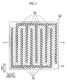
- Fig. 1 is a plan view of the back surface side of the solar cell 100 according to the first embodiment.
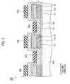
- Fig. 2 is an enlarged cross-sectional view along the A-A line of Fig. 1 .
- the solar cell 100 includes an n-type crystalline silicon substrate 10n, an i-type amorphous semiconductor layer 11i, a p-type amorphous semiconductor layer 11p, an i-type amorphous semiconductor layer 12i, an n-type amorphous semiconductor layer 12n, a p-side electrode 20p, an n-side electrode 20n, and a recombination layer R.
- the n-type crystalline silicon substrate 10n is formed of a laminated monocrystalline silicon or polycrystalline silicon.
- the n-type crystalline silicon substrate 10n includes a light receiving surface to receive sunlight and a back surface arranged on an opposite side of the light receiving surface.
- the n-type crystalline silicon substrate 10n generates a photogenerated carrier by the light received on the light receiving surface.
- the photogenerated carrier includes an electron and a hole produced when light is absorbed into the n-type crystalline silicon substrate 10n.
- a structure e.g., an electrode
- light can be received on the entire light receiving surface.
- the i-type amorphous semiconductor layer 11i is formed along a first direction on the back surface of the n-type crystalline silicon substrate 10n.
- the i-type amorphous semiconductor layer 11i is formed without actively introducing an impurity.
- the thickness of the i-type amorphous semiconductor layer 11i is about several ⁇ to 250 ⁇ , for example, i.e., substantially not as sufficient as to contribute to the electric generation.
- the p-type amorphous semiconductor layer 11p is formed along the first direction on the i-type amorphous semiconductor layer 11i.
- the p-type amorphous semiconductor layer 11p is p-type conductivity type.
- the thickness of the p-type amorphous semiconductor layer 11p is about 10 nm, for example.
- the i-type amorphous semiconductor layer 11i may not be formed, according to a structure in which the i-type amorphous semiconductor layer 11i and the p-type amorphous semiconductor layer 11p are sequentially formed on the n-type crystalline silicon substrate 10n (a so-called "HIT” (trademark, SANYO Electric Co., Ltd.) structure), it is possible to improve a pn junction characteristic.
- HIT trademark, SANYO Electric Co., Ltd.
- the i-type amorphous semiconductor layer 12i is formed to extend over the back surface of the n-type crystalline silicon substrate 10n and the p-type amorphous semiconductor layer 11p.
- the i-type amorphous semiconductor layer 12i is formed to cover an almost entire back surface of the n-type crystalline silicon substrate 10n.
- an impurity is not actively introduced.
- the thickness of the i-type amorphous semiconductor layer 12i is about several ⁇ to 250 ⁇ , for example.
- the n-type amorphous semiconductor layer 12n is formed on the i-type amorphous semiconductor layer 12i.
- the n-type amorphous semiconductor layer 12n is formed to cover the i-type amorphous semiconductor layer 12i.
- the thickness of the n-type amorphous semiconductor layer 12n is about 10 nm, for example.
- a structure in which the n-type amorphous semiconductor layer 12n is formed above the n-type crystalline silicon substrate 10n, it is possible to inhibit a recombination of minority carriers at the interface between the back surface of the n-type crystalline silicon substrate 10n and the amorphous semiconductor layer.
- the thin i-type amorphous semiconductor layer 12i is interposed between the back surface of the n-type crystalline silicon substrate 10n and the n-type amorphous semiconductor layer 12n, it is possible to improve a characteristic between the back surface of the n-type crystalline silicon substrate 10n and the n-type amorphous semiconductor layer 12n.
- each of the i-type amorphous semiconductor layer 11i, the i-type amorphous semiconductor layer 12i, the p-type amorphous semiconductor layer 11p, and the n-type amorphous semiconductor layer 12n by an amorphous semiconductor containing silicon.
- the amorphous semiconductor include amorphous silicon, amorphous silicon carbide, and amorphous silicon germanium; however, the present invention is not limited thereto, and another amorphous semiconductor may be used.
- Each of the i-type amorphous semiconductor layer 11i, the i-type amorphous semiconductor layer 12i, the p-type amorphous semiconductor layer 11p, and the n-type amorphous semiconductor layer 12n may be configured by one element of the amorphous semiconductor, and may be configured by a combination of two or more elements of the amorphous semiconductor.
- the p-side electrode 20p is a collecting electrode configured to collect a carrier.
- the p-side electrode 20p is formed above the p-type amorphous semiconductor layer 11p with the i-type amorphous semiconductor layer 12i and the n-type amorphous semiconductor layer 12n being interposed therebetween. Therefore, the p-side electrode 20p is formed in a line shape along the first direction.
- metals such as Ag and Al, a conductive paste, etc., can be used.
- the n-side electrode 20n is a collecting electrode configured to collect a carrier.
- the n-side electrode 20n is formed on the n-type amorphous semiconductor layer 12n. Therefore, the n-side electrode 20n is formed in a line shape along the first direction, between one p-side electrode 20p and another p-side electrode 20p.
- the p-side electrode 20p and the n-side electrode 20n may be a single-layered structure or a multiple-layered laminated structure.
- a transparent conductive layer may be arranged on the n-type amorphous semiconductor layer 12n side.
- the transparent conductive layer include transparent conductive oxide such as indium oxide, tin oxide, and zinc oxide.
- the p-side electrode 20p and the n-side electrode 20n may be formed to cover an approximate entire surface of the p-type amorphous semiconductor layer 11p or the n-type amorphous semiconductor layer 12n. With this formation, even when a sheet resistance of the p-type amorphous semiconductor layer 11p or the n-type amorphous semiconductor layer 12n is not too small, the carrier can be sufficiently collected by the p-side electrode 20p and the n-side electrode 20n.
- the recombination layer R is arranged to inhibit the formation of a p(i)n junction by the p-type amorphous semiconductor layer 11p, the i-type amorphous semiconductor layer 12i, and the n-type amorphous semiconductor layer 12n, at the back surface side of an n(i)p junction formed by the n-type crystalline silicon substrate 10n, the i-type amorphous semiconductor layer 11i, and the p-type amorphous semiconductor layer 11p. Therefore, in this embodiment, it is attempted to achieve a low resistance between the p-side electrode 20p and the p-type amorphous semiconductor layer 11p by the interposing of the recombination layer R.
- the recombination layer R having the above-described characteristic is formed by (1) a semiconductor material in which many in-gap levels exist in the energy band and (2) a metal material in an ohmic contact with the p-type amorphous semiconductor layer 11p.
- the thickness of the i-type amorphous semiconductor layer 12i formed on the surface of the recombination layer R is very thin, and thus, the effect as a barrier to a carrier is very small.
- the low resistance between the p-side electrode 20p and the p-type amorphous semiconductor layer 11p is achieved, and this enables good extraction of carriers from the p-side electrode 20p.
- examples of the semiconductor material configuring the recombination layer R include (i) a p-type semiconductor material containing more p-type impurities than the p-type amorphous semiconductor layer 11p, (ii) a semiconductor material containing many lattice defects, and (iii) an n-type semiconductor material containing more n-type impurities than the n-type amorphous semiconductor layer 12n.
- examples of the semiconductor material containing many lattice defects include a semiconductor material (amorphous silicon carbide and amorphous silicon germanium) in which a lattice defect is increased by mixing a foreign element, such as carbon and germanium, with an amorphous silicon, and p-type or n-type microcrystalline silicon.
- the conductivity type of the recombination layer R is of n-type, it is possible to form the recombination layer R by using the same material gas as that for the amorphous semiconductor layer 12n, and therefore, it is possible to inhibit an increase in manufacture costs.
- the contact of the both layers is achieved in a low resistance, i.e., approximates to an ohmic contact.
- the low resistance between the p-side electrode 20p and the p-type amorphous semiconductor layer 11p is achieved, and this enables good extraction of carriers from the p-side electrode 20p.
- titan (Ti), tungsten (W), etc. may be used as such a metal material.
- the thickness of the recombination layer R preferably is 0.1 to 20 nm, and more preferably is 1 to 10 nm.
- the recombination layer R is formed after the i-type amorphous semiconductor layer 11i and the p-type amorphous semiconductor layer 11p are sequentially formed on the entire back surface of the n-type crystalline silicon substrate 10n by using a CVD method,.
- the recombination layer R is formed by a semiconductor material
- the CVD method, etc. may be used
- the recombination layer R is formed by a metal material, a sputtering method and an evaporation method may be used.
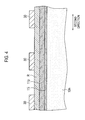
- a resist film 30 is applied in a predetermined pattern.
- the predetermined pattern corresponds to a region in which the p-side electrode 20p is formed, and set along a dashed line in Fig. 1 as a reference, for example.
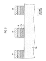
- an etching process is performed to pattern the i-type amorphous semiconductor layer 11i, the p-type amorphous semiconductor layer 11p, and the recombination layer R.
- a material etched by an etching material of the amorphous semiconductor layer is used as a material of the recombination layer R, it is possible to perform an etching process on the recombination layer R simultaneously of the i-type amorphous semiconductor layer 11i and the p-type amorphous semiconductor layer 11p, and therefore, it is preferable in view of productivity improvement.
- an etching process and a hydrogen plasma process are performed to clean an exposed region of the back surface of the n-type crystalline silicon substrate 10n. It is noted that as a result of this, the etching process and the hydrogen plasma process may also be performed on the surface of the recombination layer R.
- a CVD method is used to sequentially form the i-type amorphous semiconductor layer 12i and the n-type amorphous semiconductor layer 12n to extend over the back surface of the n-type crystalline silicon substrate 10n and the recombination layer R.
- a CVD method a sputtering method, an evaporation method, a plating method, a print method, etc., are used to form the p-side electrode 20p and the n-side electrode 20n in a predetermined pattern on the n-type amorphous semiconductor layer 12n.
- the solar cell 100 includes the recombination layer R inserted between the p-type amorphous semiconductor layer 11p and the n-type amorphous semiconductor layer 12n.
- the p-type amorphous semiconductor layer 11p and the recombination layer R contact to each other in a low resistance.
- the recombination layer R according to the first embodiment can be formed by the semiconductor material in which many in-gap levels exist in the energy band.
- the semiconductor material include a p-type semiconductor material containing more p-type impurities than the p-type amorphous semiconductor layer 11p, an n-type semiconductor material containing more n-type impurities than the n-type amorphous semiconductor layer 12n, and a microcrystalline silicon.
- the conductivity type of the recombination layer R is the same as that of the amorphous semiconductor layer 12n, it is possible to form the recombination layer R by using the same material gas as that for the amorphous semiconductor layer 12n, and therefore, it is possible to inhibit an increase in manufacture costs.
- the recombination layer R according to the first embodiment can be formed by a metal material in an ohmic contact with the p-type amorphous semiconductor layer 11p.
- the metal material include titan (Ti) and tungsten (W).
- the i-type amorphous semiconductor layer 11i, the p-type amorphous semiconductor layer 11p, and the recombination layer R are patterned, and thereafter, the i-type amorphous semiconductor layer 12i and the n-type amorphous semiconductor layer 12n are sequentially formed to extend over the back surface of the n-type crystalline silicon substrate 10n and the recombination layer R.
- the recombination layer R is formed on the p-type amorphous semiconductor layer 11p, and thus, it is not necessary to pattern the i-type amorphous semiconductor layer 12i and the n-type amorphous semiconductor layer 12n by using a mask, for example. As a result, it is possible to improve the productivity of the solar cell 100.
- Fig. 7 is an enlarged cross-sectional view of the solar cell 100 according to the second embodiment. As illustrated in Fig. 7 , the solar cell 100 includes a semiconductor layer S.
- the semiconductor layer S is interposed between the recombination layer R and the i-type amorphous semiconductor layer 12i.
- the semiconductor layer S has the same conductivity type as that of the n-type amorphous semiconductor layer 12n. Accordingly, at the back surface side of the n(i)p junction formed by the n-type crystalline silicon substrate 10n, the i-type amorphous semiconductor layer 11i, and the p-type amorphous semiconductor layer 11p, an n(i)n junction is formed by the semiconductor layer S, the i-type amorphous semiconductor layer 12i, and the n-type amorphous semiconductor layer 12n.
- the thickness of the i-type amorphous semiconductor layer 12i is very thin, the effect as a barrier against a carrier is very small. Therefore, the carrier is extracted from the p-side electrode 20p with the n-type amorphous semiconductor layer 12n being interposed.
- the conductivity type of the recombination layer R is the same as that of the amorphous semiconductor layer 12n, it is possible to form the recombination layer R, the semiconductor layer S, and the amorphous semiconductor layer 12n by using the same material gas, and therefore, it is possible to inhibit an increase in manufacture costs.
- the n-type crystalline silicon substrate 10n is used as a substrate of the solar cell 100; however, the present invention is not limited thereto.
- the substrate of the solar cell 100 may be imparted with a p-type conductivity.
- the substrate of the solar cell 100 may be configured of a general semiconductor material including a crystalline semiconductor material such as polycrystalline Si and microcrystalline Si, or a compound semiconductor material such as GaAs and InP.
- the p-type amorphous semiconductor layer 11p is formed on the back surface of the n-type crystalline silicon substrate 10n after which the n-type amorphous semiconductor layer 12n is formed.
- the present invention is not limited thereto.
- the order of forming the p-type amorphous semiconductor layer 11p and the n-type amorphous semiconductor layer 12n may be opposite. That is, the n-type amorphous semiconductor layer 12n may be formed on the back surface of the n-type crystalline silicon substrate 10n, and then, the p-type amorphous semiconductor layer 11p may be formed.
- the p-type amorphous semiconductor layer 11p and the n-type amorphous semiconductor layer 12n preferably are formed in an opposite manner to the formation of the above embodiments. That is, the p-type amorphous semiconductor layer 11p is formed to cover the i-type amorphous semiconductor layer 12i.
- the p-type amorphous semiconductor tends to have a larger electric resistance than the n-type amorphous semiconductor, and thus, it is possible to further inhibit the generation of a leakage between the p-side electrode 20p and the n-side electrode 20n.
- the i-type amorphous semiconductor layer 11i and the i-type amorphous semiconductor layer 12i are formed without actively introducing the impurities; however, only a very small amount of dopant may be included.
- the i-type amorphous semiconductor layer 13i may not be formed on the back surface of the n-type crystalline silicon substrate 10n. In this case, it is possible to further reduce the resistance on the back surface side of the n-type crystalline silicon substrate 10n.
- the p-type amorphous semiconductor layer 11p and the n-type amorphous semiconductor layer 12n are configured by an amorphous semiconductor; however, these layers 11p and 12n may be configured by an amorphous semiconductor carbide or a microcrystalline silicon.
- the recombination layer R has a one-layer structure; however, the present invention is not limited thereto.
- the recombination layer R may further include another layer capable of holding an ohmic contact with the p-type amorphous semiconductor layer 11p.
- the p-type amorphous semiconductor layer 11p has a one-layer structure; however, the present invention is not limited thereto.
- the p-type amorphous semiconductor layer 11p may further include another layer capable of holding an ohmic contact with the recombination layer R.
- the solar cell according to the present invention is useful in a solar cell manufacturing field because it is possible to provide a back junction solar cell by which it is possible to improve a solar cell characteristic.
Landscapes
- Photovoltaic Devices (AREA)
- Life Sciences & Earth Sciences (AREA)
- Engineering & Computer Science (AREA)
- Sustainable Energy (AREA)
- Sustainable Development (AREA)
Abstract
Description
- The present invention relates to a back contact solar cell.
- Solar cells can convert sunlight, which is clean and is available in unlimited amounts, directly into electricity. Therefore, solar cells are expected as a new energy source.
- Conventionally, a so-called back contact solar cell is proposed which includes a plurality of p-side electrodes and a plurality of n-side electrodes on the back surface of an n-type semiconductor substrate (see Patent Document 1, for example).
- Specifically, the solar cell according to Patent Document 1 includes: an i-type semiconductor layer covering the back surface of an n-type semiconductor substrate; a plurality of p-type semiconductor layers formed along a predetermined direction on the i-type semiconductor layer; and an n-type semiconductor layer covering the i-type semiconductor layer and the plurality of p-type semiconductor layers. Each p-side electrode is formed above each p-type semiconductor layer, with the n-type semiconductor layer being interposed therebetween. Each n-side electrode is formed between the two p-side electrodes.
- According to such a configuration, it is not necessary to cover the p-type semiconductor layer with a mask during a step of forming the n-type semiconductor layer, and thus, it is possible to simplify a step of manufacturing a solar cell.
- Patent Document 1: Japanese Unexamined Patent Application Publication No.
2005-101151 Fig. 2 ). - However, in the configuration described in Patent Document 1, an electric field in an opposite direction of the electric field formed by an n-type semiconductor substrate and a p-type semiconductor layer is formed by an n-type semiconductor layer formed on a p-type semiconductor layer and the p-type semiconductor layer. Thus, it is difficult to improve a solar cell characteristic.
- The present invention has been achieved in view of the above-described problem, and an object thereof is to provide a back contact solar cell by which it is possible to improve a solar cell characteristic.
- A solar cell according to a feature of the present invention summarized as including: a semiconductor substrate; a first semiconductor layer of first conductivity type formed on a first region on one main surface of the semiconductor substrate; and a second semiconductor layer of second conductivity type formed on a second region on the one main surface of the semiconductor substrate, wherein the second semiconductor layer is formed to extend over the second region and the first semiconductor layer, and on the first region, a recombination layer inserted between the first semiconductor layer and the second semiconductor layer is provided.
- According to a solar cell based on a characteristic of the present invention, it is possible to inhibit the formation of a reverse junction of a first semiconductor layer and a second semiconductor layer on the back surface side of a junction formed by a substrate and the first semiconductor layer. Accordingly, it is possible to reduce a carrier collection loss, and therefore, it is possible to improve a solar cell characteristic.
- In the solar cell according to the feature of the present invention, the solar cell may include: a first electrode formed on the first semiconductor layer, on the first region; and a second electrode formed on the second semiconductor layer, on the second region, wherein the first electrode may be connected to the first semiconductor layer, with the recombination layer being interposed.
- In the solar cell according to the feature of the present invention, the recombination layer may be formed of the same semiconductor as that of the second semiconductor layer, and a dopant amount contained in the recombination layer may be larger than a dopant amount contained in the second semiconductor layer.
- In the solar cell according to the feature of the present invention, the recombination layer may be formed of the same semiconductor as that of the first semiconductor layer, and a dopant amount contained in the recombination layer may be larger than a dopant amount contained in the first semiconductor layer.
- In the solar cell according to the feature of the present invention, the recombination layer may be formed of microcrystalline silicon.
- In the solar cell according to the feature of the present invention, the recombination layer may be formed of a metal.
- In the solar cell according to the feature of the present invention, the second conductivity type may be of p-type.
- In the solar cell according to the feature of the present invention, the solar cell may include a third semiconductor layer of the second conductivity type may be inserted between the recombination layer and the second semiconductor layer.
- According to the present invention, it is possible to provide a back contact solar cell by which it is possible to improve a solar cell characteristic.
-
- [
Fig. 1] Fig. 1 is a plan view of the back surface side of asolar cell 100 according to a first embodiment of the present invention. - [
Fig. 2] Fig. 2 is an enlarged cross-sectional view taken along the A-A line ofFig. 1 . - [
Fig. 3] Fig. 3 is a diagram explaining a method of manufacturing the solar cell 10 according to the first embodiment of the present invention. - [
Fig. 4] Fig. 4 is a diagram explaining the method of manufacturing the solar cell 10 according to the first embodiment of the present invention. - [
Fig. 5] Fig. 5 is a diagram explaining the method of manufacturing the solar cell 10 according to the first embodiment of the present invention. - [
Fig. 6] Fig. 6 is a diagram explaining the method of manufacturing the solar cell 10 according to the first embodiment of the present invention. - [
Fig. 7] Fig. 7 is an enlarged cross-sectional view of asolar cell 100 according to a second embodiment. - With reference to the drawings, embodiments of the present invention will be described. In the following description of the drawings, the same or similar parts will be denoted by the same or similar reference numerals. However, it should be noted that the drawings are schematic and ratios of respective dimensions and the like are different from actual ones. Therefore, the specific dimensions, etc., should be determined in consideration of the following explanations. It is needless to say that relations and ratios among the respective dimensions differ among the diagrams.
- The configuration of a
solar cell 100 according to the first embodiment of the present invention will be explained with reference toFig. 1 andFig. 2 .Fig. 1 is a plan view of the back surface side of thesolar cell 100 according to the first embodiment.Fig. 2 is an enlarged cross-sectional view along the A-A line ofFig. 1 . - As illustrated in
Fig. 1 andFig. 2 , thesolar cell 100 includes an n-typecrystalline silicon substrate 10n, an i-typeamorphous semiconductor layer 11i, a p-typeamorphous semiconductor layer 11p, an i-typeamorphous semiconductor layer 12i, an n-typeamorphous semiconductor layer 12n, a p-side electrode 20p, an n-side electrode 20n, and a recombination layer R. - The n-type
crystalline silicon substrate 10n is formed of a laminated monocrystalline silicon or polycrystalline silicon. The n-typecrystalline silicon substrate 10n includes a light receiving surface to receive sunlight and a back surface arranged on an opposite side of the light receiving surface. The n-typecrystalline silicon substrate 10n generates a photogenerated carrier by the light received on the light receiving surface. The photogenerated carrier includes an electron and a hole produced when light is absorbed into the n-typecrystalline silicon substrate 10n. Although not illustrated, it should be noted that a structure (e.g., an electrode) that prevents light being incident thereon is not formed on the light receiving surface of the n-typecrystalline silicon substrate 10n, and light can be received on the entire light receiving surface. - The i-type
amorphous semiconductor layer 11i is formed along a first direction on the back surface of the n-typecrystalline silicon substrate 10n. The i-typeamorphous semiconductor layer 11i is formed without actively introducing an impurity. The thickness of the i-typeamorphous semiconductor layer 11i is about several Å to 250 Å, for example, i.e., substantially not as sufficient as to contribute to the electric generation. - The p-type
amorphous semiconductor layer 11p is formed along the first direction on the i-typeamorphous semiconductor layer 11i. The p-typeamorphous semiconductor layer 11p is p-type conductivity type. The thickness of the p-typeamorphous semiconductor layer 11p is about 10 nm, for example. - It is noted that although the i-type
amorphous semiconductor layer 11i may not be formed, according to a structure in which the i-typeamorphous semiconductor layer 11i and the p-typeamorphous semiconductor layer 11p are sequentially formed on the n-typecrystalline silicon substrate 10n (a so-called "HIT" (trademark, SANYO Electric Co., Ltd.) structure), it is possible to improve a pn junction characteristic. - The i-type
amorphous semiconductor layer 12i is formed to extend over the back surface of the n-typecrystalline silicon substrate 10n and the p-typeamorphous semiconductor layer 11p. In the first embodiment, the i-typeamorphous semiconductor layer 12i is formed to cover an almost entire back surface of the n-typecrystalline silicon substrate 10n. When the i-typeamorphous semiconductor layer 12i is formed, an impurity is not actively introduced. The thickness of the i-typeamorphous semiconductor layer 12i is about several Å to 250Å, for example. - The n-type
amorphous semiconductor layer 12n is formed on the i-typeamorphous semiconductor layer 12i. In the first embodiment, the n-typeamorphous semiconductor layer 12n is formed to cover the i-typeamorphous semiconductor layer 12i. The thickness of the n-typeamorphous semiconductor layer 12n is about 10 nm, for example. - According to a structure (a so-called "BSF structure") in which the n-type
amorphous semiconductor layer 12n is formed above the n-typecrystalline silicon substrate 10n, it is possible to inhibit a recombination of minority carriers at the interface between the back surface of the n-typecrystalline silicon substrate 10n and the amorphous semiconductor layer. - It is noted that according to a structure in which the thin i-type
amorphous semiconductor layer 12i is interposed between the back surface of the n-typecrystalline silicon substrate 10n and the n-typeamorphous semiconductor layer 12n, it is possible to improve a characteristic between the back surface of the n-typecrystalline silicon substrate 10n and the n-typeamorphous semiconductor layer 12n. - In this case, it is possible to configure each of the i-type
amorphous semiconductor layer 11i, the i-typeamorphous semiconductor layer 12i, the p-typeamorphous semiconductor layer 11p, and the n-typeamorphous semiconductor layer 12n by an amorphous semiconductor containing silicon. Examples of the amorphous semiconductor include amorphous silicon, amorphous silicon carbide, and amorphous silicon germanium; however, the present invention is not limited thereto, and another amorphous semiconductor may be used. Each of the i-typeamorphous semiconductor layer 11i, the i-typeamorphous semiconductor layer 12i, the p-typeamorphous semiconductor layer 11p, and the n-typeamorphous semiconductor layer 12n may be configured by one element of the amorphous semiconductor, and may be configured by a combination of two or more elements of the amorphous semiconductor. - The p-
side electrode 20p is a collecting electrode configured to collect a carrier. The p-side electrode 20p is formed above the p-typeamorphous semiconductor layer 11p with the i-typeamorphous semiconductor layer 12i and the n-typeamorphous semiconductor layer 12n being interposed therebetween. Therefore, the p-side electrode 20p is formed in a line shape along the first direction. - As the p-
side electrode 20p, metals such as Ag and Al, a conductive paste, etc., can be used. - The n-
side electrode 20n is a collecting electrode configured to collect a carrier. The n-side electrode 20n is formed on the n-typeamorphous semiconductor layer 12n. Therefore, the n-side electrode 20n is formed in a line shape along the first direction, between one p-side electrode 20p and another p-side electrode 20p. - It is noted that the p-
side electrode 20p and the n-side electrode 20n may be a single-layered structure or a multiple-layered laminated structure. When the laminated structure is employed, a transparent conductive layer may be arranged on the n-typeamorphous semiconductor layer 12n side. Examples of the transparent conductive layer include transparent conductive oxide such as indium oxide, tin oxide, and zinc oxide. - The p-
side electrode 20p and the n-side electrode 20n may be formed to cover an approximate entire surface of the p-typeamorphous semiconductor layer 11p or the n-typeamorphous semiconductor layer 12n. With this formation, even when a sheet resistance of the p-typeamorphous semiconductor layer 11p or the n-typeamorphous semiconductor layer 12n is not too small, the carrier can be sufficiently collected by the p-side electrode 20p and the n-side electrode 20n. - The recombination layer R is arranged to inhibit the formation of a p(i)n junction by the p-type
amorphous semiconductor layer 11p, the i-typeamorphous semiconductor layer 12i, and the n-typeamorphous semiconductor layer 12n, at the back surface side of an n(i)p junction formed by the n-typecrystalline silicon substrate 10n, the i-typeamorphous semiconductor layer 11i, and the p-typeamorphous semiconductor layer 11p. Therefore, in this embodiment, it is attempted to achieve a low resistance between the p-side electrode 20p and the p-typeamorphous semiconductor layer 11p by the interposing of the recombination layer R. - The recombination layer R having the above-described characteristic is formed by (1) a semiconductor material in which many in-gap levels exist in the energy band and (2) a metal material in an ohmic contact with the p-type
amorphous semiconductor layer 11p. - When such a semiconductor material is used, if a carrier recombination by way of many in-gap levels existing in the energy band being is utilized, then it is possible to extract the carriers generated on the n-type
crystalline silicon substrate 10n, with the p-typeamorphous semiconductor layer 11p being interposed. Therefore, even when the recombination layer R is formed on the surface of the p-typeamorphous semiconductor layer 11p, the contact of the both layers is achieved in a low resistance, i.e., approximates to an ohmic contact. - As described above, the thickness of the i-type
amorphous semiconductor layer 12i formed on the surface of the recombination layer R is very thin, and thus, the effect as a barrier to a carrier is very small. - Thus, the low resistance between the p-
side electrode 20p and the p-typeamorphous semiconductor layer 11p is achieved, and this enables good extraction of carriers from the p-side electrode 20p. - In this case, examples of the semiconductor material configuring the recombination layer R include (i) a p-type semiconductor material containing more p-type impurities than the p-type
amorphous semiconductor layer 11p, (ii) a semiconductor material containing many lattice defects, and (iii) an n-type semiconductor material containing more n-type impurities than the n-typeamorphous semiconductor layer 12n. Examples of the semiconductor material containing many lattice defects include a semiconductor material (amorphous silicon carbide and amorphous silicon germanium) in which a lattice defect is increased by mixing a foreign element, such as carbon and germanium, with an amorphous silicon, and p-type or n-type microcrystalline silicon. - It is noted that when the conductivity type of the recombination layer R is of n-type, it is possible to form the recombination layer R by using the same material gas as that for the
amorphous semiconductor layer 12n, and therefore, it is possible to inhibit an increase in manufacture costs. - When such a metal material is used, even if the recombination layer R is formed on the surface of the p-type
amorphous semiconductor layer 11p, the contact of the both layers is achieved in a low resistance, i.e., approximates to an ohmic contact. Thus, the low resistance between the p-side electrode 20p and the p-typeamorphous semiconductor layer 11p is achieved, and this enables good extraction of carriers from the p-side electrode 20p. - It is noted that as such a metal material, titan (Ti), tungsten (W), etc., may be used.
- In order to inhibit an increase in a resistance component, the thickness of the recombination layer R preferably is 0.1 to 20 nm, and more preferably is 1 to 10 nm.
- Next, the method of manufacturing the
solar cell 100 will be described with reference to the cross-sectional surface of thesolar cell 100. - Firstly, as illustrated in
Fig. 3 , the recombination layer R is formed after the i-typeamorphous semiconductor layer 11i and the p-typeamorphous semiconductor layer 11p are sequentially formed on the entire back surface of the n-typecrystalline silicon substrate 10n by using a CVD method,. When the recombination layer R is formed by a semiconductor material, the CVD method, etc., may be used, and when the recombination layer R is formed by a metal material, a sputtering method and an evaporation method may be used. - Subsequently, as illustrated in
Fig. 4 , on the recombination layer R, a resistfilm 30 is applied in a predetermined pattern. The predetermined pattern corresponds to a region in which the p-side electrode 20p is formed, and set along a dashed line inFig. 1 as a reference, for example. - Subsequently, as illustrated in
Fig. 5 , an etching process is performed to pattern the i-typeamorphous semiconductor layer 11i, the p-typeamorphous semiconductor layer 11p, and the recombination layer R. At this time, when a material etched by an etching material of the amorphous semiconductor layer is used as a material of the recombination layer R, it is possible to perform an etching process on the recombination layer R simultaneously of the i-typeamorphous semiconductor layer 11i and the p-typeamorphous semiconductor layer 11p, and therefore, it is preferable in view of productivity improvement. Subsequently, after the removal of the resistfilm 30, an etching process and a hydrogen plasma process are performed to clean an exposed region of the back surface of the n-typecrystalline silicon substrate 10n. It is noted that as a result of this, the etching process and the hydrogen plasma process may also be performed on the surface of the recombination layer R. - Subsequently, as illustrated in
Fig. 6 , a CVD method is used to sequentially form the i-typeamorphous semiconductor layer 12i and the n-typeamorphous semiconductor layer 12n to extend over the back surface of the n-typecrystalline silicon substrate 10n and the recombination layer R. - Next, a CVD method, a sputtering method, an evaporation method, a plating method, a print method, etc., are used to form the p-
side electrode 20p and the n-side electrode 20n in a predetermined pattern on the n-typeamorphous semiconductor layer 12n. - The
solar cell 100 according to the first embodiment includes the recombination layer R inserted between the p-typeamorphous semiconductor layer 11p and the n-typeamorphous semiconductor layer 12n. The p-typeamorphous semiconductor layer 11p and the recombination layer R contact to each other in a low resistance. - This inhibits the electric field in an opposite direction of the electric field formed by the n-type
crystalline silicon substrate 10n, the i-typeamorphous semiconductor layer 11i, and the p-typeamorphous semiconductor layer 11p from being formed by the p-typeamorphous semiconductor layer 11p, the i-typeamorphous semiconductor layer 12i, and the n-typeamorphous semiconductor layer 12n. Therefore, the low resistance between the p-side electrode 20p and the p-typeamorphous semiconductor layer 11p is achieved, and this enables good extraction of carriers from the p-side electrode 20p. As a result, it is possible to reduce a carrier collection loss, and therefore, it is possible to improve a characteristic of thesolar cell 100. - The recombination layer R according to the first embodiment can be formed by the semiconductor material in which many in-gap levels exist in the energy band. In this case, when a carrier recombination by way of many in-gap levels in the energy band being is utilized, then it is possible to extract the carriers generated on the n-type
crystalline silicon substrate 10n, with the p-typeamorphous semiconductor layer 11p being interposed. Examples of the semiconductor material include a p-type semiconductor material containing more p-type impurities than the p-typeamorphous semiconductor layer 11p, an n-type semiconductor material containing more n-type impurities than the n-typeamorphous semiconductor layer 12n, and a microcrystalline silicon. In particular, when the conductivity type of the recombination layer R is the same as that of theamorphous semiconductor layer 12n, it is possible to form the recombination layer R by using the same material gas as that for theamorphous semiconductor layer 12n, and therefore, it is possible to inhibit an increase in manufacture costs. - The recombination layer R according to the first embodiment can be formed by a metal material in an ohmic contact with the p-type
amorphous semiconductor layer 11p. Examples of the metal material include titan (Ti) and tungsten (W). - In the method of manufacturing the
solar cell 100 according to the first embodiment, the i-typeamorphous semiconductor layer 11i, the p-typeamorphous semiconductor layer 11p, and the recombination layer R are patterned, and thereafter, the i-typeamorphous semiconductor layer 12i and the n-typeamorphous semiconductor layer 12n are sequentially formed to extend over the back surface of the n-typecrystalline silicon substrate 10n and the recombination layer R. - In this way, the recombination layer R is formed on the p-type
amorphous semiconductor layer 11p, and thus, it is not necessary to pattern the i-typeamorphous semiconductor layer 12i and the n-typeamorphous semiconductor layer 12n by using a mask, for example. As a result, it is possible to improve the productivity of thesolar cell 100. - Hereinafter, a
solar cell 100 according to a second embodiment will be described with reference to drawings. The description below is based primarily on the differences with respect to the first embodiment. -
Fig. 7 is an enlarged cross-sectional view of thesolar cell 100 according to the second embodiment. As illustrated inFig. 7 , thesolar cell 100 includes a semiconductor layer S. - The semiconductor layer S is interposed between the recombination layer R and the i-type
amorphous semiconductor layer 12i. The semiconductor layer S has the same conductivity type as that of the n-typeamorphous semiconductor layer 12n. Accordingly, at the back surface side of the n(i)p junction formed by the n-typecrystalline silicon substrate 10n, the i-typeamorphous semiconductor layer 11i, and the p-typeamorphous semiconductor layer 11p, an n(i)n junction is formed by the semiconductor layer S, the i-typeamorphous semiconductor layer 12i, and the n-typeamorphous semiconductor layer 12n. - Thus, even when the n(i)n junction is formed at the back surface side of the n(i)p junction, since the thickness of the i-type
amorphous semiconductor layer 12i is very thin, the effect as a barrier against a carrier is very small. Therefore, the carrier is extracted from the p-side electrode 20p with the n-typeamorphous semiconductor layer 12n being interposed. - It is noted that when the conductivity type of the recombination layer R is the same as that of the
amorphous semiconductor layer 12n, it is possible to form the recombination layer R, the semiconductor layer S, and theamorphous semiconductor layer 12n by using the same material gas, and therefore, it is possible to inhibit an increase in manufacture costs. - Although the present invention has been described with reference to the above embodiments, it should be understood that the present invention is not limited to the description and drawings which constitute a part of this disclosure. From this disclosure, various alternative embodiments, examples and operational technologies will become apparent to those skilled in the art.
- For example, in the above embodiments, the n-type
crystalline silicon substrate 10n is used as a substrate of thesolar cell 100; however, the present invention is not limited thereto. For example, the substrate of thesolar cell 100 may be imparted with a p-type conductivity. Moreover, the substrate of thesolar cell 100 may be configured of a general semiconductor material including a crystalline semiconductor material such as polycrystalline Si and microcrystalline Si, or a compound semiconductor material such as GaAs and InP. - Moreover, in the above-described embodiments, the p-type
amorphous semiconductor layer 11p is formed on the back surface of the n-typecrystalline silicon substrate 10n after which the n-typeamorphous semiconductor layer 12n is formed. However, the present invention is not limited thereto. For example, the order of forming the p-typeamorphous semiconductor layer 11p and the n-typeamorphous semiconductor layer 12n may be opposite. That is, the n-typeamorphous semiconductor layer 12n may be formed on the back surface of the n-typecrystalline silicon substrate 10n, and then, the p-typeamorphous semiconductor layer 11p may be formed. - Although there is no particular description in the above-described embodiments, when a p-type substrate is used, the p-type
amorphous semiconductor layer 11p and the n-typeamorphous semiconductor layer 12n preferably are formed in an opposite manner to the formation of the above embodiments. That is, the p-typeamorphous semiconductor layer 11p is formed to cover the i-typeamorphous semiconductor layer 12i. In this case, generally, the p-type amorphous semiconductor tends to have a larger electric resistance than the n-type amorphous semiconductor, and thus, it is possible to further inhibit the generation of a leakage between the p-side electrode 20p and the n-side electrode 20n. - In the above-described embodiments, the i-type
amorphous semiconductor layer 11i and the i-typeamorphous semiconductor layer 12i are formed without actively introducing the impurities; however, only a very small amount of dopant may be included. - Although there is no particular description in the above-described embodiments, the i-type amorphous semiconductor layer 13i may not be formed on the back surface of the n-type
crystalline silicon substrate 10n. In this case, it is possible to further reduce the resistance on the back surface side of the n-typecrystalline silicon substrate 10n. - Moreover, in the embodiments, the p-type
amorphous semiconductor layer 11p and the n-typeamorphous semiconductor layer 12n are configured by an amorphous semiconductor; however, theselayers - In the embodiments, the recombination layer R has a one-layer structure; however, the present invention is not limited thereto. The recombination layer R may further include another layer capable of holding an ohmic contact with the p-type
amorphous semiconductor layer 11p. - In the embodiments, the p-type
amorphous semiconductor layer 11p has a one-layer structure; however, the present invention is not limited thereto. The p-typeamorphous semiconductor layer 11p may further include another layer capable of holding an ohmic contact with the recombination layer R. - It is noted that the entire contents of Japanese Patent Application No.
2009-44431 (filed on February 26, 2009 - Thus, the solar cell according to the present invention is useful in a solar cell manufacturing field because it is possible to provide a back junction solar cell by which it is possible to improve a solar cell characteristic.
-
- 10
- SOLAR CELL
- 10n
- n-TYPE CRYSTALLINE SILICON SUBSTRATE
- 11i
- i-TYPE AMORPHOUS SEMICONDUCTOR LAYER
- 11p
- p-TYPE AMORPHOUS SEMICONDUCTOR LAYER
- 111P
- SUBSTRATE SIDE REGION
- 112P
- RECOMBINATION LAYER SIDE REGION
- 12i
- i-TYPE AMORPHOUS SEMICONDUCTOR LAYER
- 12n
- n-TYPE AMORPHOUS SEMICONDUCTOR LAYER
- 20n
- n-SIDE ELECTRODE
- 20p
- p-SIDE ELECTRODE
- 30
- RESIST FILM
- R
- RECOMBINATION LAYER
- S
- SEMICONDUCTOR LAYER
- 100
- SOLAR CELL
Claims (8)
- A solar cell, comprising:a semiconductor substrate;a first semiconductor layer of first conductivity type formed on a first region on one main surface of the semiconductor substrate; anda second semiconductor layer of second conductivity type formed on a second region on the one main surface of the semiconductor substrate, whereinthe second semiconductor layer is formed to extend over the second region and the first semiconductor layer, andon the first region, a recombination layer inserted between the first semiconductor layer and the second semiconductor layer is provided.
- The solar cell according to claim 1, comprising:a first electrode formed on the first semiconductor layer, on the first region; anda second electrode formed on the second semiconductor layer, on the second region, whereinthe first electrode is connected to the first semiconductor layer, with the recombination layer being interposed.
- The solar cell according to claim 1 or 2, wherein
the recombination layer is formed of the same semiconductor as that of the second semiconductor layer, and
a dopant amount contained in the recombination layer is larger than a dopant amount contained in the second semiconductor layer. - The solar cell according to any one of claims 1 to 3, wherein the recombination layer is formed of the same semiconductor as that of the first semiconductor layer, and
a dopant amount contained in the recombination layer is larger than a dopant amount contained in the first semiconductor layer. - The solar cell according to claim 1 or 2, wherein the recombination layer is formed of microcrystalline silicon.
- The solar cell according to claim 1 or 2, wherein the recombination layer is formed of a metal.
- The solar cell according to any one of claims 1 to 6, wherein the second conductivity type is of p-type.
- The solar cell according to any one of claims 1 to 7, comprising a third semiconductor layer of the second conductivity type inserted between the recombination layer and the second semiconductor layer.
Applications Claiming Priority (2)
| Application Number | Priority Date | Filing Date | Title |
|---|---|---|---|
| JP2009044431A JP5461028B2 (en) | 2009-02-26 | 2009-02-26 | Solar cell |
| PCT/JP2010/053086 WO2010098445A1 (en) | 2009-02-26 | 2010-02-26 | Solaer cell |
Publications (3)
| Publication Number | Publication Date |
|---|---|
| EP2403004A1 true EP2403004A1 (en) | 2012-01-04 |
| EP2403004A4 EP2403004A4 (en) | 2017-07-19 |
| EP2403004B1 EP2403004B1 (en) | 2021-03-31 |
Family
ID=42665649
Family Applications (1)
| Application Number | Title | Priority Date | Filing Date |
|---|---|---|---|
| EP10746324.2A Active EP2403004B1 (en) | 2009-02-26 | 2010-02-26 | Solar cell |
Country Status (5)
| Country | Link |
|---|---|
| US (1) | US8927853B2 (en) |
| EP (1) | EP2403004B1 (en) |
| JP (1) | JP5461028B2 (en) |
| CN (1) | CN102422434B (en) |
| WO (1) | WO2010098445A1 (en) |
Cited By (1)
| Publication number | Priority date | Publication date | Assignee | Title |
|---|---|---|---|---|
| DE112012006605B4 (en) | 2012-06-29 | 2021-10-14 | Panasonic Intellectual Property Management Co., Ltd. | Solar cell |
Families Citing this family (19)
| Publication number | Priority date | Publication date | Assignee | Title |
|---|---|---|---|---|
| JPWO2012132766A1 (en) | 2011-03-28 | 2014-07-28 | 三洋電機株式会社 | Photoelectric conversion device and method of manufacturing photoelectric conversion device |
| JP2013030615A (en) * | 2011-07-28 | 2013-02-07 | Sanyo Electric Co Ltd | Solar cell |
| JP6208682B2 (en) * | 2011-12-21 | 2017-10-04 | サンパワー コーポレイション | Hybrid polysilicon heterojunction back contact battery |
| DE112012006595T5 (en) * | 2012-06-29 | 2015-04-02 | Sanyo Electric Co., Ltd. | solar cell |
| WO2014016932A1 (en) * | 2012-07-26 | 2014-01-30 | 三洋電機株式会社 | Solar-cell manufacturing method and solar cell |
| WO2014016931A1 (en) * | 2012-07-26 | 2014-01-30 | 三洋電機株式会社 | Solar cell and manufacturing method therefor |
| CN102856328B (en) * | 2012-10-10 | 2015-06-10 | 友达光电股份有限公司 | Solar cell and manufacturing method thereof |
| JP6013198B2 (en) * | 2013-01-04 | 2016-10-25 | シャープ株式会社 | Photoelectric conversion element and method for producing photoelectric conversion element |
| JP6013200B2 (en) * | 2013-01-09 | 2016-10-25 | シャープ株式会社 | Photoelectric conversion element and method for producing photoelectric conversion element |
| JP6284522B2 (en) * | 2013-03-28 | 2018-02-28 | シャープ株式会社 | Photoelectric conversion element, photoelectric conversion module, and photovoltaic power generation system |
| WO2017111697A1 (en) * | 2015-12-24 | 2017-06-29 | Trina Solar Energy Development Pte Ltd. | A method of fabricating a heterojunction all-back-contact solar cell |
| US10217878B2 (en) | 2016-04-01 | 2019-02-26 | Sunpower Corporation | Tri-layer semiconductor stacks for patterning features on solar cells |
| CN110047965A (en) * | 2018-01-16 | 2019-07-23 | 福建金石能源有限公司 | A kind of novel back contacts hetero-junction solar cell and preparation method thereof |
| CN114744063B (en) * | 2020-12-23 | 2023-08-08 | 泰州隆基乐叶光伏科技有限公司 | Solar cell, production method and photovoltaic module |
| WO2022134991A1 (en) * | 2020-12-23 | 2022-06-30 | 泰州隆基乐叶光伏科技有限公司 | Solar cell and production method, and photovoltaic module |
| CN113380950B (en) * | 2021-05-12 | 2024-07-19 | 郑州轻工业大学 | A back contact perovskite solar cell and preparation method thereof |
| CN117317036A (en) * | 2022-06-24 | 2023-12-29 | 泰州隆基乐叶光伏科技有限公司 | A back contact battery and its manufacturing method |
| CN115995500A (en) * | 2022-10-28 | 2023-04-21 | 天合光能股份有限公司 | Solar cell and its preparation method |
| CN116722053B (en) * | 2023-08-09 | 2023-10-27 | 天合光能股份有限公司 | Solar cell, preparation method thereof and photovoltaic module |
Family Cites Families (10)
| Publication number | Priority date | Publication date | Assignee | Title |
|---|---|---|---|---|
| US4396793A (en) * | 1982-04-12 | 1983-08-02 | Chevron Research Company | Compensated amorphous silicon solar cell |
| DE3420887A1 (en) * | 1984-06-05 | 1985-12-05 | Telefunken electronic GmbH, 7100 Heilbronn | SOLAR CELL |
| JP4155899B2 (en) * | 2003-09-24 | 2008-09-24 | 三洋電機株式会社 | Photovoltaic element manufacturing method |
| CN100431177C (en) | 2003-09-24 | 2008-11-05 | 三洋电机株式会社 | Photovoltaic element and manufacturing method thereof |
| JP3998619B2 (en) * | 2003-09-24 | 2007-10-31 | 三洋電機株式会社 | Photovoltaic element and manufacturing method thereof |
| JP2009152222A (en) | 2006-10-27 | 2009-07-09 | Kyocera Corp | Method for manufacturing solar cell element |
| WO2008140601A1 (en) * | 2006-12-06 | 2008-11-20 | Solexant Corporation | Nanophotovoltaic device with improved quantum efficiency |
| JP5166745B2 (en) * | 2007-03-07 | 2013-03-21 | 信越化学工業株式会社 | Method for producing single crystal silicon solar cell |
| JP2009044431A (en) | 2007-08-08 | 2009-02-26 | Funai Electric Co Ltd | Portable telephone terminal |
| EP2239788A4 (en) * | 2008-01-30 | 2017-07-12 | Kyocera Corporation | Solar battery element and solar battery element manufacturing method |
-
2009
- 2009-02-26 JP JP2009044431A patent/JP5461028B2/en not_active Expired - Fee Related
-
2010
- 2010-02-26 US US13/203,513 patent/US8927853B2/en not_active Expired - Fee Related
- 2010-02-26 CN CN201080018626.5A patent/CN102422434B/en not_active Expired - Fee Related
- 2010-02-26 EP EP10746324.2A patent/EP2403004B1/en active Active
- 2010-02-26 WO PCT/JP2010/053086 patent/WO2010098445A1/en not_active Ceased
Non-Patent Citations (1)
| Title |
|---|
| See references of WO2010098445A1 * |
Cited By (1)
| Publication number | Priority date | Publication date | Assignee | Title |
|---|---|---|---|---|
| DE112012006605B4 (en) | 2012-06-29 | 2021-10-14 | Panasonic Intellectual Property Management Co., Ltd. | Solar cell |
Also Published As
| Publication number | Publication date |
|---|---|
| EP2403004A4 (en) | 2017-07-19 |
| WO2010098445A1 (en) | 2010-09-02 |
| CN102422434A (en) | 2012-04-18 |
| US20120090674A1 (en) | 2012-04-19 |
| JP5461028B2 (en) | 2014-04-02 |
| EP2403004B1 (en) | 2021-03-31 |
| CN102422434B (en) | 2015-09-02 |
| US8927853B2 (en) | 2015-01-06 |
| JP2010199415A (en) | 2010-09-09 |
Similar Documents
| Publication | Publication Date | Title |
|---|---|---|
| EP2403004B1 (en) | Solar cell | |
| US9006564B2 (en) | Method of manufacturing solar cell and solar cell | |
| US12610653B2 (en) | Solar cell, preparation method thereof and photovoltaic module | |
| US8664034B2 (en) | Method of manufacturing solar cell | |
| EP2530729B1 (en) | Solar cell and method for producing same | |
| CN103283033B (en) | The manufacture method of solar cell and solar cell | |
| JP6792053B2 (en) | Solar cell | |
| US20120325309A1 (en) | Solar cell and solar cell manufacturing method | |
| JP2005101240A (en) | Photovoltaic element and manufacturing method thereof | |
| EP2600414A1 (en) | Process for production of solar cell, and solar cell | |
| WO2020180244A1 (en) | Solar cell and method for fabricating a solar cell | |
| WO2015070250A1 (en) | Dielectric-passivated metal insulator photovoltaic solar cells | |
| JP2008085374A (en) | Photovoltaic element | |
| EP3664156A1 (en) | Solar cell and electronic device provided with said solar cell | |
| JP2005101427A (en) | Photovoltaic element and manufacturing method thereof | |
| US20120012176A1 (en) | Solar cell and method of manufacturing the same | |
| JP4945916B2 (en) | Photoelectric conversion element | |
| WO2015023709A2 (en) | Silicon wafers with p-n junctions by epitaxial deposition and devices fabricated therefrom | |
| JP5816800B2 (en) | Manufacturing method of solar cell | |
| TWI517423B (en) | Back-mounted solar cell manufacturing method |
Legal Events
| Date | Code | Title | Description |
|---|---|---|---|
| PUAI | Public reference made under article 153(3) epc to a published international application that has entered the european phase |
Free format text: ORIGINAL CODE: 0009012 |
|
| 17P | Request for examination filed |
Effective date: 20110909 |
|
| AK | Designated contracting states |
Kind code of ref document: A1 Designated state(s): AT BE BG CH CY CZ DE DK EE ES FI FR GB GR HR HU IE IS IT LI LT LU LV MC MK MT NL NO PL PT RO SE SI SK SM TR |
|
| RTI1 | Title (correction) |
Free format text: SOLAR CELL |
|
| DAX | Request for extension of the european patent (deleted) | ||
| RAP1 | Party data changed (applicant data changed or rights of an application transferred) |
Owner name: PANASONIC INTELLECTUAL PROPERTY MANAGEMENT CO., LT |
|
| RA4 | Supplementary search report drawn up and despatched (corrected) |
Effective date: 20170616 |
|
| RIC1 | Information provided on ipc code assigned before grant |
Ipc: H01L 31/0224 20060101AFI20170609BHEP Ipc: H01L 31/20 20060101ALI20170609BHEP Ipc: H01L 31/0747 20120101ALI20170609BHEP |
|
| STAA | Information on the status of an ep patent application or granted ep patent |
Free format text: STATUS: EXAMINATION IS IN PROGRESS |
|
| 17Q | First examination report despatched |
Effective date: 20200525 |
|
| REG | Reference to a national code |
Ref country code: DE Ref legal event code: R079 Ref document number: 602010066688 Country of ref document: DE Free format text: PREVIOUS MAIN CLASS: H01L0031040000 Ipc: H01L0031022400 |
|
| GRAP | Despatch of communication of intention to grant a patent |
Free format text: ORIGINAL CODE: EPIDOSNIGR1 |
|
| STAA | Information on the status of an ep patent application or granted ep patent |
Free format text: STATUS: GRANT OF PATENT IS INTENDED |
|
| RIC1 | Information provided on ipc code assigned before grant |
Ipc: H01L 31/0224 20060101AFI20201030BHEP Ipc: H01L 31/0747 20120101ALI20201030BHEP |
|
| INTG | Intention to grant announced |
Effective date: 20201120 |
|
| GRAS | Grant fee paid |
Free format text: ORIGINAL CODE: EPIDOSNIGR3 |
|
| GRAA | (expected) grant |
Free format text: ORIGINAL CODE: 0009210 |
|
| STAA | Information on the status of an ep patent application or granted ep patent |
Free format text: STATUS: THE PATENT HAS BEEN GRANTED |
|
| AK | Designated contracting states |
Kind code of ref document: B1 Designated state(s): AT BE BG CH CY CZ DE DK EE ES FI FR GB GR HR HU IE IS IT LI LT LU LV MC MK MT NL NO PL PT RO SE SI SK SM TR |
|
| REG | Reference to a national code |
Ref country code: GB Ref legal event code: FG4D Ref country code: CH Ref legal event code: EP |
|
| REG | Reference to a national code |
Ref country code: AT Ref legal event code: REF Ref document number: 1377928 Country of ref document: AT Kind code of ref document: T Effective date: 20210415 |
|
| REG | Reference to a national code |
Ref country code: DE Ref legal event code: R096 Ref document number: 602010066688 Country of ref document: DE |
|
| REG | Reference to a national code |
Ref country code: IE Ref legal event code: FG4D |
|
| REG | Reference to a national code |
Ref country code: LT Ref legal event code: MG9D |
|
| PG25 | Lapsed in a contracting state [announced via postgrant information from national office to epo] |
Ref country code: NO Free format text: LAPSE BECAUSE OF FAILURE TO SUBMIT A TRANSLATION OF THE DESCRIPTION OR TO PAY THE FEE WITHIN THE PRESCRIBED TIME-LIMIT Effective date: 20210630 Ref country code: BG Free format text: LAPSE BECAUSE OF FAILURE TO SUBMIT A TRANSLATION OF THE DESCRIPTION OR TO PAY THE FEE WITHIN THE PRESCRIBED TIME-LIMIT Effective date: 20210630 Ref country code: HR Free format text: LAPSE BECAUSE OF FAILURE TO SUBMIT A TRANSLATION OF THE DESCRIPTION OR TO PAY THE FEE WITHIN THE PRESCRIBED TIME-LIMIT Effective date: 20210331 Ref country code: FI Free format text: LAPSE BECAUSE OF FAILURE TO SUBMIT A TRANSLATION OF THE DESCRIPTION OR TO PAY THE FEE WITHIN THE PRESCRIBED TIME-LIMIT Effective date: 20210331 |
|
| PG25 | Lapsed in a contracting state [announced via postgrant information from national office to epo] |
Ref country code: LV Free format text: LAPSE BECAUSE OF FAILURE TO SUBMIT A TRANSLATION OF THE DESCRIPTION OR TO PAY THE FEE WITHIN THE PRESCRIBED TIME-LIMIT Effective date: 20210331 Ref country code: SE Free format text: LAPSE BECAUSE OF FAILURE TO SUBMIT A TRANSLATION OF THE DESCRIPTION OR TO PAY THE FEE WITHIN THE PRESCRIBED TIME-LIMIT Effective date: 20210331 |
|
| REG | Reference to a national code |
Ref country code: NL Ref legal event code: MP Effective date: 20210331 |
|
| REG | Reference to a national code |
Ref country code: AT Ref legal event code: MK05 Ref document number: 1377928 Country of ref document: AT Kind code of ref document: T Effective date: 20210331 |
|
| PG25 | Lapsed in a contracting state [announced via postgrant information from national office to epo] |
Ref country code: NL Free format text: LAPSE BECAUSE OF FAILURE TO SUBMIT A TRANSLATION OF THE DESCRIPTION OR TO PAY THE FEE WITHIN THE PRESCRIBED TIME-LIMIT Effective date: 20210331 Ref country code: LT Free format text: LAPSE BECAUSE OF FAILURE TO SUBMIT A TRANSLATION OF THE DESCRIPTION OR TO PAY THE FEE WITHIN THE PRESCRIBED TIME-LIMIT Effective date: 20210331 Ref country code: EE Free format text: LAPSE BECAUSE OF FAILURE TO SUBMIT A TRANSLATION OF THE DESCRIPTION OR TO PAY THE FEE WITHIN THE PRESCRIBED TIME-LIMIT Effective date: 20210331 Ref country code: CZ Free format text: LAPSE BECAUSE OF FAILURE TO SUBMIT A TRANSLATION OF THE DESCRIPTION OR TO PAY THE FEE WITHIN THE PRESCRIBED TIME-LIMIT Effective date: 20210331 Ref country code: SM Free format text: LAPSE BECAUSE OF FAILURE TO SUBMIT A TRANSLATION OF THE DESCRIPTION OR TO PAY THE FEE WITHIN THE PRESCRIBED TIME-LIMIT Effective date: 20210331 Ref country code: AT Free format text: LAPSE BECAUSE OF FAILURE TO SUBMIT A TRANSLATION OF THE DESCRIPTION OR TO PAY THE FEE WITHIN THE PRESCRIBED TIME-LIMIT Effective date: 20210331 |
|
| PG25 | Lapsed in a contracting state [announced via postgrant information from national office to epo] |
Ref country code: RO Free format text: LAPSE BECAUSE OF FAILURE TO SUBMIT A TRANSLATION OF THE DESCRIPTION OR TO PAY THE FEE WITHIN THE PRESCRIBED TIME-LIMIT Effective date: 20210331 Ref country code: IS Free format text: LAPSE BECAUSE OF FAILURE TO SUBMIT A TRANSLATION OF THE DESCRIPTION OR TO PAY THE FEE WITHIN THE PRESCRIBED TIME-LIMIT Effective date: 20210731 Ref country code: ES Free format text: LAPSE BECAUSE OF FAILURE TO SUBMIT A TRANSLATION OF THE DESCRIPTION OR TO PAY THE FEE WITHIN THE PRESCRIBED TIME-LIMIT Effective date: 20210331 Ref country code: SK Free format text: LAPSE BECAUSE OF FAILURE TO SUBMIT A TRANSLATION OF THE DESCRIPTION OR TO PAY THE FEE WITHIN THE PRESCRIBED TIME-LIMIT Effective date: 20210331 Ref country code: PL Free format text: LAPSE BECAUSE OF FAILURE TO SUBMIT A TRANSLATION OF THE DESCRIPTION OR TO PAY THE FEE WITHIN THE PRESCRIBED TIME-LIMIT Effective date: 20210331 Ref country code: PT Free format text: LAPSE BECAUSE OF FAILURE TO SUBMIT A TRANSLATION OF THE DESCRIPTION OR TO PAY THE FEE WITHIN THE PRESCRIBED TIME-LIMIT Effective date: 20210802 |
|
| REG | Reference to a national code |
Ref country code: DE Ref legal event code: R097 Ref document number: 602010066688 Country of ref document: DE |
|
| PG25 | Lapsed in a contracting state [announced via postgrant information from national office to epo] |
Ref country code: DK Free format text: LAPSE BECAUSE OF FAILURE TO SUBMIT A TRANSLATION OF THE DESCRIPTION OR TO PAY THE FEE WITHIN THE PRESCRIBED TIME-LIMIT Effective date: 20210331 |
|
| PLBE | No opposition filed within time limit |
Free format text: ORIGINAL CODE: 0009261 |
|
| STAA | Information on the status of an ep patent application or granted ep patent |
Free format text: STATUS: NO OPPOSITION FILED WITHIN TIME LIMIT |
|
| 26N | No opposition filed |
Effective date: 20220104 |
|
| PG25 | Lapsed in a contracting state [announced via postgrant information from national office to epo] |
Ref country code: IS Free format text: LAPSE BECAUSE OF FAILURE TO SUBMIT A TRANSLATION OF THE DESCRIPTION OR TO PAY THE FEE WITHIN THE PRESCRIBED TIME-LIMIT Effective date: 20210731 |
|
| PG25 | Lapsed in a contracting state [announced via postgrant information from national office to epo] |
Ref country code: IT Free format text: LAPSE BECAUSE OF FAILURE TO SUBMIT A TRANSLATION OF THE DESCRIPTION OR TO PAY THE FEE WITHIN THE PRESCRIBED TIME-LIMIT Effective date: 20210331 |
|
| REG | Reference to a national code |
Ref country code: DE Ref legal event code: R119 Ref document number: 602010066688 Country of ref document: DE |
|
| PG25 | Lapsed in a contracting state [announced via postgrant information from national office to epo] |
Ref country code: MC Free format text: LAPSE BECAUSE OF FAILURE TO SUBMIT A TRANSLATION OF THE DESCRIPTION OR TO PAY THE FEE WITHIN THE PRESCRIBED TIME-LIMIT Effective date: 20210331 |
|
| REG | Reference to a national code |
Ref country code: CH Ref legal event code: PL |
|
| REG | Reference to a national code |
Ref country code: BE Ref legal event code: MM Effective date: 20220228 |
|
| GBPC | Gb: european patent ceased through non-payment of renewal fee |
Effective date: 20220226 |
|
| PG25 | Lapsed in a contracting state [announced via postgrant information from national office to epo] |
Ref country code: LU Free format text: LAPSE BECAUSE OF NON-PAYMENT OF DUE FEES Effective date: 20220226 |
|
| PG25 | Lapsed in a contracting state [announced via postgrant information from national office to epo] |
Ref country code: FR Free format text: LAPSE BECAUSE OF NON-PAYMENT OF DUE FEES Effective date: 20220228 |
|
| PG25 | Lapsed in a contracting state [announced via postgrant information from national office to epo] |
Ref country code: LI Free format text: LAPSE BECAUSE OF NON-PAYMENT OF DUE FEES Effective date: 20220228 Ref country code: IE Free format text: LAPSE BECAUSE OF NON-PAYMENT OF DUE FEES Effective date: 20220226 Ref country code: GB Free format text: LAPSE BECAUSE OF NON-PAYMENT OF DUE FEES Effective date: 20220226 Ref country code: DE Free format text: LAPSE BECAUSE OF NON-PAYMENT OF DUE FEES Effective date: 20220901 Ref country code: CH Free format text: LAPSE BECAUSE OF NON-PAYMENT OF DUE FEES Effective date: 20220228 |
|
| PG25 | Lapsed in a contracting state [announced via postgrant information from national office to epo] |
Ref country code: BE Free format text: LAPSE BECAUSE OF NON-PAYMENT OF DUE FEES Effective date: 20220228 |
|
| PG25 | Lapsed in a contracting state [announced via postgrant information from national office to epo] |
Ref country code: HU Free format text: LAPSE BECAUSE OF FAILURE TO SUBMIT A TRANSLATION OF THE DESCRIPTION OR TO PAY THE FEE WITHIN THE PRESCRIBED TIME-LIMIT; INVALID AB INITIO Effective date: 20100226 |
|
| PG25 | Lapsed in a contracting state [announced via postgrant information from national office to epo] |
Ref country code: MK Free format text: LAPSE BECAUSE OF FAILURE TO SUBMIT A TRANSLATION OF THE DESCRIPTION OR TO PAY THE FEE WITHIN THE PRESCRIBED TIME-LIMIT Effective date: 20210331 Ref country code: CY Free format text: LAPSE BECAUSE OF FAILURE TO SUBMIT A TRANSLATION OF THE DESCRIPTION OR TO PAY THE FEE WITHIN THE PRESCRIBED TIME-LIMIT Effective date: 20210331 |
|
| PG25 | Lapsed in a contracting state [announced via postgrant information from national office to epo] |
Ref country code: MT Free format text: LAPSE BECAUSE OF FAILURE TO SUBMIT A TRANSLATION OF THE DESCRIPTION OR TO PAY THE FEE WITHIN THE PRESCRIBED TIME-LIMIT Effective date: 20210331 |
|
| PG25 | Lapsed in a contracting state [announced via postgrant information from national office to epo] |
Ref country code: GR Free format text: LAPSE BECAUSE OF NON-PAYMENT OF DUE FEES Effective date: 20210331 |
|
| PG25 | Lapsed in a contracting state [announced via postgrant information from national office to epo] |
Ref country code: GR Free format text: LAPSE BECAUSE OF NON-PAYMENT OF DUE FEES Effective date: 20210331 |
|
| PG25 | Lapsed in a contracting state [announced via postgrant information from national office to epo] |
Ref country code: TR Free format text: LAPSE BECAUSE OF FAILURE TO SUBMIT A TRANSLATION OF THE DESCRIPTION OR TO PAY THE FEE WITHIN THE PRESCRIBED TIME-LIMIT Effective date: 20210331 |