EP2402959A1 - Flexible cable and transmission system - Google Patents
Flexible cable and transmission system Download PDFInfo
- Publication number
- EP2402959A1 EP2402959A1 EP10761390A EP10761390A EP2402959A1 EP 2402959 A1 EP2402959 A1 EP 2402959A1 EP 10761390 A EP10761390 A EP 10761390A EP 10761390 A EP10761390 A EP 10761390A EP 2402959 A1 EP2402959 A1 EP 2402959A1
- Authority
- EP
- European Patent Office
- Prior art keywords
- signal
- flexible cable
- differential
- shield member
- wire
- Prior art date
- Legal status (The legal status is an assumption and is not a legal conclusion. Google has not performed a legal analysis and makes no representation as to the accuracy of the status listed.)
- Granted
Links
Images




Classifications
-
- H—ELECTRICITY
- H01—ELECTRIC ELEMENTS
- H01B—CABLES; CONDUCTORS; INSULATORS; SELECTION OF MATERIALS FOR THEIR CONDUCTIVE, INSULATING OR DIELECTRIC PROPERTIES
- H01B7/00—Insulated conductors or cables characterised by their form
- H01B7/08—Flat or ribbon cables
- H01B7/0838—Parallel wires, sandwiched between two insulating layers
-
- H—ELECTRICITY
- H04—ELECTRIC COMMUNICATION TECHNIQUE
- H04B—TRANSMISSION
- H04B3/00—Line transmission systems
- H04B3/02—Details
-
- H—ELECTRICITY
- H05—ELECTRIC TECHNIQUES NOT OTHERWISE PROVIDED FOR
- H05K—PRINTED CIRCUITS; CASINGS OR CONSTRUCTIONAL DETAILS OF ELECTRIC APPARATUS; MANUFACTURE OF ASSEMBLAGES OF ELECTRICAL COMPONENTS
- H05K1/00—Printed circuits
- H05K1/02—Details
- H05K1/0213—Electrical arrangements not otherwise provided for
- H05K1/0216—Reduction of cross-talk, noise or electromagnetic interference
- H05K1/0218—Reduction of cross-talk, noise or electromagnetic interference by printed shielding conductors, ground planes or power plane
- H05K1/0224—Patterned shielding planes, ground planes or power planes
-
- H—ELECTRICITY
- H05—ELECTRIC TECHNIQUES NOT OTHERWISE PROVIDED FOR
- H05K—PRINTED CIRCUITS; CASINGS OR CONSTRUCTIONAL DETAILS OF ELECTRIC APPARATUS; MANUFACTURE OF ASSEMBLAGES OF ELECTRICAL COMPONENTS
- H05K1/00—Printed circuits
- H05K1/02—Details
- H05K1/0213—Electrical arrangements not otherwise provided for
- H05K1/0237—High frequency adaptations
- H05K1/0248—Skew reduction or using delay lines
-
- H—ELECTRICITY
- H01—ELECTRIC ELEMENTS
- H01B—CABLES; CONDUCTORS; INSULATORS; SELECTION OF MATERIALS FOR THEIR CONDUCTIVE, INSULATING OR DIELECTRIC PROPERTIES
- H01B11/00—Communication cables or conductors
- H01B11/02—Cables with twisted pairs or quads
- H01B11/06—Cables with twisted pairs or quads with means for reducing effects of electromagnetic or electrostatic disturbances, e.g. screens
- H01B11/10—Screens specially adapted for reducing interference from external sources
- H01B11/1091—Screens specially adapted for reducing interference from external sources with screen grounding means, e.g. drain wires
-
- H—ELECTRICITY
- H01—ELECTRIC ELEMENTS
- H01B—CABLES; CONDUCTORS; INSULATORS; SELECTION OF MATERIALS FOR THEIR CONDUCTIVE, INSULATING OR DIELECTRIC PROPERTIES
- H01B7/00—Insulated conductors or cables characterised by their form
- H01B7/08—Flat or ribbon cables
- H01B7/0861—Flat or ribbon cables comprising one or more screens
-
- H—ELECTRICITY
- H05—ELECTRIC TECHNIQUES NOT OTHERWISE PROVIDED FOR
- H05K—PRINTED CIRCUITS; CASINGS OR CONSTRUCTIONAL DETAILS OF ELECTRIC APPARATUS; MANUFACTURE OF ASSEMBLAGES OF ELECTRICAL COMPONENTS
- H05K1/00—Printed circuits
- H05K1/02—Details
- H05K1/0213—Electrical arrangements not otherwise provided for
- H05K1/0216—Reduction of cross-talk, noise or electromagnetic interference
- H05K1/0218—Reduction of cross-talk, noise or electromagnetic interference by printed shielding conductors, ground planes or power plane
- H05K1/0219—Printed shielding conductors for shielding around or between signal conductors, e.g. coplanar or coaxial printed shielding conductors
-
- H—ELECTRICITY
- H05—ELECTRIC TECHNIQUES NOT OTHERWISE PROVIDED FOR
- H05K—PRINTED CIRCUITS; CASINGS OR CONSTRUCTIONAL DETAILS OF ELECTRIC APPARATUS; MANUFACTURE OF ASSEMBLAGES OF ELECTRICAL COMPONENTS
- H05K1/00—Printed circuits
- H05K1/02—Details
- H05K1/0213—Electrical arrangements not otherwise provided for
- H05K1/0237—High frequency adaptations
- H05K1/0245—Lay-out of balanced signal pairs, e.g. differential lines or twisted lines
-
- H—ELECTRICITY
- H05—ELECTRIC TECHNIQUES NOT OTHERWISE PROVIDED FOR
- H05K—PRINTED CIRCUITS; CASINGS OR CONSTRUCTIONAL DETAILS OF ELECTRIC APPARATUS; MANUFACTURE OF ASSEMBLAGES OF ELECTRICAL COMPONENTS
- H05K1/00—Printed circuits
- H05K1/02—Details
- H05K1/03—Use of materials for the substrate
- H05K1/0393—Flexible materials
-
- H—ELECTRICITY
- H05—ELECTRIC TECHNIQUES NOT OTHERWISE PROVIDED FOR
- H05K—PRINTED CIRCUITS; CASINGS OR CONSTRUCTIONAL DETAILS OF ELECTRIC APPARATUS; MANUFACTURE OF ASSEMBLAGES OF ELECTRICAL COMPONENTS
- H05K2201/00—Indexing scheme relating to printed circuits covered by H05K1/00
- H05K2201/07—Electric details
- H05K2201/0707—Shielding
- H05K2201/0715—Shielding provided by an outer layer of PCB
-
- H—ELECTRICITY
- H05—ELECTRIC TECHNIQUES NOT OTHERWISE PROVIDED FOR
- H05K—PRINTED CIRCUITS; CASINGS OR CONSTRUCTIONAL DETAILS OF ELECTRIC APPARATUS; MANUFACTURE OF ASSEMBLAGES OF ELECTRICAL COMPONENTS
- H05K2201/00—Indexing scheme relating to printed circuits covered by H05K1/00
- H05K2201/09—Shape and layout
- H05K2201/09209—Shape and layout details of conductors
- H05K2201/09218—Conductive traces
- H05K2201/09236—Parallel layout
-
- H—ELECTRICITY
- H05—ELECTRIC TECHNIQUES NOT OTHERWISE PROVIDED FOR
- H05K—PRINTED CIRCUITS; CASINGS OR CONSTRUCTIONAL DETAILS OF ELECTRIC APPARATUS; MANUFACTURE OF ASSEMBLAGES OF ELECTRICAL COMPONENTS
- H05K2201/00—Indexing scheme relating to printed circuits covered by H05K1/00
- H05K2201/09—Shape and layout
- H05K2201/09209—Shape and layout details of conductors
- H05K2201/0929—Conductive planes
- H05K2201/093—Layout of power planes, ground planes or power supply conductors, e.g. having special clearance holes therein
-
- H—ELECTRICITY
- H05—ELECTRIC TECHNIQUES NOT OTHERWISE PROVIDED FOR
- H05K—PRINTED CIRCUITS; CASINGS OR CONSTRUCTIONAL DETAILS OF ELECTRIC APPARATUS; MANUFACTURE OF ASSEMBLAGES OF ELECTRICAL COMPONENTS
- H05K2201/00—Indexing scheme relating to printed circuits covered by H05K1/00
- H05K2201/09—Shape and layout
- H05K2201/09209—Shape and layout details of conductors
- H05K2201/0929—Conductive planes
- H05K2201/09354—Ground conductor along edge of main surface
-
- H—ELECTRICITY
- H05—ELECTRIC TECHNIQUES NOT OTHERWISE PROVIDED FOR
- H05K—PRINTED CIRCUITS; CASINGS OR CONSTRUCTIONAL DETAILS OF ELECTRIC APPARATUS; MANUFACTURE OF ASSEMBLAGES OF ELECTRICAL COMPONENTS
- H05K2201/00—Indexing scheme relating to printed circuits covered by H05K1/00
- H05K2201/09—Shape and layout
- H05K2201/09209—Shape and layout details of conductors
- H05K2201/09654—Shape and layout details of conductors covering at least two types of conductors provided for in H05K2201/09218 - H05K2201/095
- H05K2201/09718—Clearance holes
Definitions
- the present invention relates to a flexible cable of which the transmission characteristic and the electromagnetic noise characteristic are considered, and a transmission system.
- Fig. 14 is a cross sectional view of a conventional flexible cable.
- a word of "flexible cable” is used in meanings of both of FPC (Flexible Printed Circuits) and FFC (Flexible Flat Cable).
- the flexible cable 36 shown in Fig. 14 is an FPC (Flexible printed Circuits).
- the flexible cable 36 includes a flexible sheet-like base member (a dielectric substance) 1, an adhesive (a dielectric substance) 2 which bonds the base member 1 to a cover member (a dielectric substance) 3, a shield member 4 which covers the cover member 3 and is bonded or printed on the cover member 3 to suppress electromagnetic noises to be radiated, and a top coating member 5 which covers the shield member 4 to protect the shield member 4.
- the adhesive (the dielectric substance) 2 is provided therein with differential signal wires 6 through which differential signals pass, a low-speed signal wire 8 through which low-speed signals pass, ground wires 9 used as the ground and shield ground wires 10 which cause the electric potential of the shield member 4 to be identical to the electric potential of the ground.
- the shield member 4 is provided over the entirety of the flexible cable 36 so as to effectively suppress electromagnetic noises to be radiated (see Patent Document 1).
- This invention is made to solve the above described problems, and the purpose of the invention is to provide a flexible cable which is configured such that a signal wire through which a signal requiring ensuring of a transmission characteristic in a high frequency band passes, is not covered with a shield member, but a signal wire through which a signal such as a clock signal or the like to be an electromagnetic noise passes, is covered with a shield member so as to make it possible to satisfy both of ensuring of the transmission characteristic in the high frequency band and suppression of electromagnetic noises to be radiated.
- the additional purpose of the invention is to provide a transmission system having a unit of adjusting a timing of a signal arriving at an IC as a signal reception section so as to allow the IC as the signal reception section to accurately receive the signal.
- a flexible cable of the present invention includes a sheet-like dielectric substance, first and second conductive wire groups provided in the sheet-like dielectric substance, and a sheet-like shield member that is laminated on the sheet-like dielectric substance so as to cover the first conductive wire group and so as not to cover the second conductive wire group.
- a transmission system of the invention includes a signal transmission section that transmits a differential signal, a signal reception section that receives a differential signal, and a flexible cable that connects the signal transmission section to the signal reception section, and the flexible cable includes a sheet-like dielectric substance, first and second conductive wire groups provided in the sheet-like dielectric substance, and a sheet-like shield member that is laminated on the sheet-like dielectric substance so as to cover the first conductive wire group and so as not to cover the second conductive wire group.
- a flexible cable according to a first embodiment of the invention is described while schematically indicating a cross sectional view in Fig. 1 and a top view in Fig. 2 .
- a flexible cable 11 which is an FPC (Flexible Printed Circuits) includes a sheet-like base member (a dielectric substance) 1 made of a flexible material, an adhesive (a dielectric substance) 2 which bonds the base member 1 to a cover member (a dielectric substance) 3, a shield member 4 which covers the cover member 3 and is bonded or printed to the cover member 3 to suppress electromagnetic noises to be radiated, and a top coating member 5 which covers the shield member 4 to protect the shield member 4.
- FPC Flexible Printed Circuits
- the flexible cable 11 has a differential signal wire group 7 including differential signal wires 6 through which differential signals pass and guard ground wires 9a which prevent the interference from other differential signals, a low-speed signal wire 8 through which low-speed signals pass, a ground wire 9 used as the ground, and a shield ground wire 10 which is adapted to allow the electric potential of the shield member 4 to be identical to the electric potential of the ground, all of which are provided in the adhesive 2.
- the shield ground wire 10 is adapted to allow the electric potentials of the shield member 4 and the ground wire 10 to be identical to each other, and the shield member 4 and the ground wire 10 are connected to each other with a conductive adhesive, a conductive through-hole, a solder or the like.
- the differential signal wires 6 are not covered with the shield member 4. This is because that the transmission characteristic of wiring of the flexible cable 11 is markedly varied depending on presence or absence of the shield member 4.
- Fig. 3 schematically shows a transmission characteristic 12 of wiring without a shield member and a transmission characteristic 13 of wiring with a shield member.
- the transmission characteristic 13 of the wiring with the shield member is markedly deteriorated in a high frequency band as compared to the transmission characteristic 12 of the wiring without the shield member.
- a frequency band of a signal to be transmitted is a band of a comparatively low frequency such as, for example, Standard Definition picture data (SD_data)
- SD_data Standard Definition picture data
- the frequency band of a signal to be transmitted is a band of a higher frequency such as, for example, High Definition picture data (HD_data). Therefore, when the transmission characteristic is deteriorated, a shape of the transmitted signal is deformed, and thereby the transmission system does not accurately operate.
- HD_data High Definition picture data
- the flexible cable of the embodiment is configured such that the differential signal wire group 7 is not covered with the shield member 4. Accordingly, the differential signal wire group 7 can ensure the adequate transmission characteristic even in the high frequency band of signals passing through the signal wires.
- the low-speed signal wire 8, a power source wire or the ground wire 9, which is other signal wires not included in the differential signal wire group 7, is configured to be covered with the shield member 4. This is because that a signal used in low-speed communication such as 12C passing through the low-speed signal wire 8, a signal for controlling or also a power source to be supplied to an IC may become a source of electromagnetic noises. With this configuration, it is possible to suppress electromagnetic noises to be radiated.
- the flexible cable 11 is configured such that the differential signal wire group 7 is not covered with the shield member 4 and the signal wires other than the above, such as the low-speed signal wire 8 and the like are covered with the shield member 4 so that it is possible to satisfy both of ensuring of a transmission characteristic in a high frequency band and suppression of electromagnetic noises to be radiated.
- a differential signal wire or a guard ground wire is provided on a region not covered with the shield member 4, and the low-speed signal wire, the power source wire, the ground wire or the like is provided on a region covered with the shield member 4.
- the guard ground wire 9a is not necessarily included in the differential signal wire group 7.
- a flexible cable 14 according to a second embodiment of the invention is described while schematically indicating a cross sectional view in Fig. 4 and a top view in Fig. 5 .
- a kind of each signal wire covered with the shield member 4 and the top coating member 5 of the flexible cable 14 is different from that of the flexible cable according to the first embodiment.
- the entirety of the differential signal wire group 7 is not covered with the shield member 4 and the top coating member 5.
- the differential signal wire group 7 is divided differential data signal wires 6a through which data signals pass and differential clock signal wires 6b through which clock signals pass, and wires other than a differential signal wire group 7a including the differential data signal wires 6a through which data signals pass and the guard ground wire 9a, are covered with the shield member 4 and the top coating member 5.
- the LVDS transmits, for example, seven data signals 16 in one cycle of a clock signal 15 as shown in Fig. 6 . Therefore, in a case where the clock signal is set to, for example, 75 MHz, each of the data signals becomes 525 Mbps in maximum (262.5 MHz in maximum) so that the data signal becomes a high speed signal as compared to the clock signal.
- the clock signal becomes a signal of an electromagnetic noise source.
- the differential data signal wires 6a through which data signals pass to be not covered with the shield member 4 it is possible to ensure an adequate transmission characteristic in a high frequency band, and by configuring the differential clock signal wires 6b through which clock signals pass to be covered with the shield member 4, it is possible to more effectively suppress electromagnetic noises to be radiated.
- the flexible cable 14 is configured such that the differential clock signal wires 6b through which clock signals pass are covered with the shield member 4 and the differential data signal wires 6a through which data signals pass are not covered with the shield member 4. Consequently, it is possible to satisfy both of the effective suppressing of electromagnetic noises to be radiated and ensuring of the adequate transmission characteristic in the high frequency band.
- the differential signal wire or the guard ground wire is provided on a region not covered with the shield member 4, and the low-speed signal wire, the power source wire, the ground wire or the like is provided on a region covered with the shield member 4.
- the configuration is not indicated in the drawings, and only things relating to allocation of wires, which is the advantage of the invention, are indicated.
- the guard ground wire 9a is not necessarily included in the differential signal wire group 7.
- the description of the flexible cable 14 according to this embodiment is made based on the example having the configuration in which the transmission is performed by using the LVDS as the transmission method.
- a configuration in which the transmission is performed by a differential transmission method such as a miniLVDS, a BusLVDS, an RSDS, a TMDS or the like can be similarly practiced.
- a transmission system 24 includes a transmission side printed board 23a having an IC 18 as a signal transmission section, an impedance network 20 as an adjusting unit, a differential signal wire 22a and a connector 17a, and a reception side printed board 23b having a connector 17b, a differential signal wire 22b, the impedance network 20, a terminating resistor 21 and an IC 19 as a signal reception section.
- the transmission system 24 is configured such that the transmission side printed board 23a and the reception side printed board 23b are coupled to each other with the flexible cable 14.
- a first unit is configured such that the impedance network 20 is connected to a differential signal wire 22 and is adapted to perform adjusting of timing of a signal that arrives at the IC 19 as the signal reception section.
- an impedance device 27 is connected to each of the differential signal wires 22 in series or in parallel at a portion just behind the IC 18 as the signal transmission section or just in front of the IC 19 as the signal reception section. Accordingly, when the impedance of each wire is changed and the transmission speed is adjusted, the timing of each signal is adjusted.
- the amount of delay of the clock signal 15 is increased as compared to the amount of delay of the data signal 16. Therefore, the impedance device 27 (a resistor in this embodiment) are respectively connected in serial to the differential data signal wires 6a through which the data signals 16 pass so that the timing of each data signal 16 is delayed by a degree of difference in the amount of delay between the clock signal 15 and the data signal 16.
- the impedance network is referred to as the resistor.
- the resistor can be replaced with another device including an impedance component.
- a second unit is adapted to adjust a timing of outputting each signal from the IC 18 as the signal transmission section.
- FIG. 10 An output section of the LVDS of the IC 18 as the signal transmission section is schematically shown in Fig. 10 .
- the data signal 16 is converted from a parallel signal into a serial signal by a parallel-serial converter 28 to be output, and the clock signal 15 is output via a PLL (Phase Lock Loop) 30 and a divider 29.
- PLL Phase Lock Loop
- the data signal 16 When the data signal is converted by the parallel-serial converter 28, the data signal 16 is bit-shifted by the degree of difference in the amount of delay between the clock signal 15 and the data signal 16. Consequently, the signals can be output by deviating the timings thereof in advance as in a data signal 31 before bit-shifting and a data signal 32 after bit-shifting as shown in Fig. 11 .
- the PLL 30 is configured to have an oscillator 33 as a reference, two dividers 29, a phase comparator 34 and a VCO (Voltage Controlled Oscillator) 35.
- VCO Voltage Controlled Oscillator
- the VCO 35 is configured to have several invertors.
- a signal passing through the invertors has a short delay between an input section and an output section.
- the delay is utilized and the amount of delay is selected to output the clock signal so that it is possible to output the clock signal by delaying the timing of the clock signal beforehand.
- bit-shifting is performed by a degree of the increased amount of delay so as to adjust the timing of outputting the data signal from the IC 18 as the signal transmission section. Further, the timing of outputting the clock signal from the IC 18 as the signal transmission section is adjusted by using the VCO 35. Consequently, the timings of outputting the clock signal 15 and the data signal 16 from the IC 18 as the signal transmission section are adjusted.
- timing can be adjusted only by the bit-shifting or the VCO 35.
- the VCO 35 formed by combining the several invertors can be replaced with another buffer.
- the third unit is adapted to adjust a timing of a signal arriving at the IC 19 as the signal reception section in accordance with a length of the signal wire connecting the IC 18 as the signal transmission section to the IC 19 as the signal reception section.
- the timing can be adjusted by carrying out shortening of a length of a signal wire having a large amount of delay, carrying out lengthening of a length of a signal wire having a small amount of delay, or carrying out both of the shortening and the lengthening.
- the arrival time of each signal to the IC 19 as the signal reception section can be adjusted. Consequently, the timing of each signal can be adjusted.
- the IC 19 of the signal reception section can accurately receive each signal.
- the invention can be applied to a deviation in timing due to an IC as the signal transmission section, an IC as the signal reception section, wires on a board, a connector or the like other than the flexible cable 14.
- the flexible cable according to the invention makes it possible to satisfy both of ensuring of the adequate transmission characteristic in the high frequency band and suppression of electromagnetic noises to be radiated, and the invention is useful for the transmission and the transmission system with the use of the flexible cable in which the transmission characteristic and the electromagnetic noise characteristic are considered.
Landscapes
- Engineering & Computer Science (AREA)
- Microelectronics & Electronic Packaging (AREA)
- Computer Networks & Wireless Communication (AREA)
- Signal Processing (AREA)
- Physics & Mathematics (AREA)
- Electromagnetism (AREA)
- Shielding Devices Or Components To Electric Or Magnetic Fields (AREA)
- Insulated Conductors (AREA)
- Structure Of Printed Boards (AREA)
- Cable Transmission Systems, Equalization Of Radio And Reduction Of Echo (AREA)
- Communication Cables (AREA)
Abstract
Description
- The present invention relates to a flexible cable of which the transmission characteristic and the electromagnetic noise characteristic are considered, and a transmission system.
-
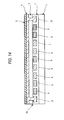
Fig. 14 is a cross sectional view of a conventional flexible cable. In this specification, a word of "flexible cable" is used in meanings of both of FPC (Flexible Printed Circuits) and FFC (Flexible Flat Cable). - The
flexible cable 36 shown inFig. 14 is an FPC (Flexible printed Circuits). Theflexible cable 36 includes a flexible sheet-like base member (a dielectric substance) 1, an adhesive (a dielectric substance) 2 which bonds thebase member 1 to a cover member (a dielectric substance) 3, ashield member 4 which covers thecover member 3 and is bonded or printed on thecover member 3 to suppress electromagnetic noises to be radiated, and atop coating member 5 which covers theshield member 4 to protect theshield member 4. The adhesive (the dielectric substance) 2 is provided therein withdifferential signal wires 6 through which differential signals pass, a low-speed signal wire 8 through which low-speed signals pass,ground wires 9 used as the ground andshield ground wires 10 which cause the electric potential of theshield member 4 to be identical to the electric potential of the ground. - Here, the
shield member 4 is provided over the entirety of theflexible cable 36 so as to effectively suppress electromagnetic noises to be radiated (see Patent Document 1). -
- Patent Document 1:
JP-A-2002-117726 - However, in a conventional flexible cable, a problem that a transmission characteristic of a signal wire covered with a shield member is markedly deteriorated in a high frequency band may arise.
- In addition, while, also in a printed board or the like, an entirety including an electromagnetic noise source is sometimes covered with a shield member such as a shield case or the like so as to suppress electromagnetic noises to be radiated, the shield member and the signal wire are away from one another, so that the transmission characteristic of the signal wire is not markedly deteriorated. However, since the flexible cable is formed in a thin sheet, the distance between the shield member and the signal wire is short, so that deterioration of the transmission characteristic of the signal wire covered with the shield member in the high frequency band has been outstanding.
- This invention is made to solve the above described problems, and the purpose of the invention is to provide a flexible cable which is configured such that a signal wire through which a signal requiring ensuring of a transmission characteristic in a high frequency band passes, is not covered with a shield member, but a signal wire through which a signal such as a clock signal or the like to be an electromagnetic noise passes, is covered with a shield member so as to make it possible to satisfy both of ensuring of the transmission characteristic in the high frequency band and suppression of electromagnetic noises to be radiated.
- In addition, in the above flexible cable, transmission speeds of signals are differentiated between the signal wire which is covered with the shield member and the signal wire which is not covered with the shield member so that timings of the signals arriving at an IC as a signal reception section are deviated from one another. Consequently, there is a possibility that the signals are not accurately received by the IC as the signal reception section. The additional purpose of the invention is to provide a transmission system having a unit of adjusting a timing of a signal arriving at an IC as a signal reception section so as to allow the IC as the signal reception section to accurately receive the signal.
- A flexible cable of the present invention includes a sheet-like dielectric substance, first and second conductive wire groups provided in the sheet-like dielectric substance, and a sheet-like shield member that is laminated on the sheet-like dielectric substance so as to cover the first conductive wire group and so as not to cover the second conductive wire group.
- Also, a transmission system of the invention includes a signal transmission section that transmits a differential signal, a signal reception section that receives a differential signal, and a flexible cable that connects the signal transmission section to the signal reception section, and the flexible cable includes a sheet-like dielectric substance, first and second conductive wire groups provided in the sheet-like dielectric substance, and a sheet-like shield member that is laminated on the sheet-like dielectric substance so as to cover the first conductive wire group and so as not to cover the second conductive wire group.
- In each of the flexible cable and the transmission system according to the invention, a signal wire through which a signal requiring ensuring of a transmission characteristic in a high frequency band passes, is not covered with a shield member, and a signal wire through which a signal to be an electromagnetic noise source passes, is covered with a shield member. Consequently, the transmission characteristic in the high frequency band can be ensured and radiation of electromagnetic noises can be suppressed.
-
- [
Fig. 1] Fig. 1 is a cross sectional view showing a flexible cable according to a first embodiment of the invention. - [
Fig. 2] Fig. 2 is a top view showing the flexible cable according to the first embodiment of the invention. - [
Fig. 3] Fig. 3 is a graph showing a relationship between a shield member and a transmission characteristic. - [
Fig. 4] Fig. 4 is a cross sectional view showing a flexible cable according to a second embodiment of the invention. - [
Fig. 5] Fig. 5 is a top view showing the flexible cable according to the second embodiment of the invention. - [
Fig. 6] Fig. 6 is a diagram showing timings of a clock and data in an LVDS. - [
Fig. 7] Fig. 7 is a configuration view showing a transmission system according to the second embodiment of the invention. - [
Fig. 8] Fig. 8 is a diagram showing waveforms in delaying of a signal by the flexible cable according to the second embodiment of the invention. - [
Fig. 9] Fig. 9 is a configuration view showing an impedance network. - [
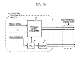
Fig. 10] Fig. 10 is a schematic view showing an LVDS output section of an IC in a signal transmission section. - [
Fig. 11] Fig. 11 is a diagram showing timings in bit-shifting. - [
Fig. 12] Fig. 12 is a configuration view showing a PLL. - [
Fig. 13] Fig. 13 is a configuration view showing a VCO. - [
Fig. 14] Fig. 14 is a cross sectional view showing a conventional flexible cable. - A flexible cable according to embodiments of the invention will be described below with reference to accompanying drawings.
- A flexible cable according to a first embodiment of the invention is described while schematically indicating a cross sectional view in
Fig. 1 and a top view inFig. 2 . - In
Fig. 1 , aflexible cable 11 which is an FPC (Flexible Printed Circuits) includes a sheet-like base member (a dielectric substance) 1 made of a flexible material, an adhesive (a dielectric substance) 2 which bonds thebase member 1 to a cover member (a dielectric substance) 3, ashield member 4 which covers thecover member 3 and is bonded or printed to thecover member 3 to suppress electromagnetic noises to be radiated, and atop coating member 5 which covers theshield member 4 to protect theshield member 4. - In addition, the
flexible cable 11 has a differentialsignal wire group 7 includingdifferential signal wires 6 through which differential signals pass andguard ground wires 9a which prevent the interference from other differential signals, a low-speed signal wire 8 through which low-speed signals pass, aground wire 9 used as the ground, and ashield ground wire 10 which is adapted to allow the electric potential of theshield member 4 to be identical to the electric potential of the ground, all of which are provided in theadhesive 2. - The
shield ground wire 10 is adapted to allow the electric potentials of theshield member 4 and theground wire 10 to be identical to each other, and theshield member 4 and theground wire 10 are connected to each other with a conductive adhesive, a conductive through-hole, a solder or the like. - The characteristics of the
flexible cable 11 having the above configuration are described with reference toFig. 3 . - First, in the embodiment, the
differential signal wires 6 are not covered with theshield member 4. This is because that the transmission characteristic of wiring of theflexible cable 11 is markedly varied depending on presence or absence of theshield member 4. -
Fig. 3 schematically shows atransmission characteristic 12 of wiring without a shield member and atransmission characteristic 13 of wiring with a shield member. - The
transmission characteristic 13 of the wiring with the shield member is markedly deteriorated in a high frequency band as compared to thetransmission characteristic 12 of the wiring without the shield member. - This is because that a distance between the shield member used in the flexible cable and the signal wire is short, and an effectiveness of the shield member as the ground is low.
- In a conventional transmission system with the use of a flexible cable, since a frequency band of a signal to be transmitted is a band of a comparatively low frequency such as, for example, Standard Definition picture data (SD_data), the transmission system operates without a trouble even when the transmission characteristic is deteriorated.
- However, in the embodiment, the frequency band of a signal to be transmitted is a band of a higher frequency such as, for example, High Definition picture data (HD_data). Therefore, when the transmission characteristic is deteriorated, a shape of the transmitted signal is deformed, and thereby the transmission system does not accurately operate.
- Therefore, the flexible cable of the embodiment is configured such that the differential
signal wire group 7 is not covered with theshield member 4. Accordingly, the differentialsignal wire group 7 can ensure the adequate transmission characteristic even in the high frequency band of signals passing through the signal wires. - In addition, the low-
speed signal wire 8, a power source wire or theground wire 9, which is other signal wires not included in the differentialsignal wire group 7, is configured to be covered with theshield member 4. This is because that a signal used in low-speed communication such as 12C passing through the low-speed signal wire 8, a signal for controlling or also a power source to be supplied to an IC may become a source of electromagnetic noises. With this configuration, it is possible to suppress electromagnetic noises to be radiated. - Thus, in accordance with the
flexible cable 11 according to the first embodiment of the invention, theflexible cable 11 is configured such that the differentialsignal wire group 7 is not covered with theshield member 4 and the signal wires other than the above, such as the low-speed signal wire 8 and the like are covered with theshield member 4 so that it is possible to satisfy both of ensuring of a transmission characteristic in a high frequency band and suppression of electromagnetic noises to be radiated. - Meanwhile, regarding the wiring in the
flexible cable 11, in addition to the wires having the number shown in the drawings, a differential signal wire or a guard ground wire is provided on a region not covered with theshield member 4, and the low-speed signal wire, the power source wire, the ground wire or the like is provided on a region covered with theshield member 4. However, in the above description, the configuration is not indicated in the drawings, and only things relating to allocation of wires, which is the advantage of the invention, are indicated. Theguard ground wire 9a is not necessarily included in the differentialsignal wire group 7. - Next, a
flexible cable 14 according to a second embodiment of the invention is described while schematically indicating a cross sectional view inFig. 4 and a top view inFig. 5 . - In
Fig. 4 , a kind of each signal wire covered with theshield member 4 and thetop coating member 5 of theflexible cable 14 is different from that of the flexible cable according to the first embodiment. - In the first embodiment, the entirety of the differential
signal wire group 7 is not covered with theshield member 4 and thetop coating member 5. Contrary to the above, in this embodiment, the differentialsignal wire group 7 is divided differentialdata signal wires 6a through which data signals pass and differentialclock signal wires 6b through which clock signals pass, and wires other than a differentialsignal wire group 7a including the differentialdata signal wires 6a through which data signals pass and theguard ground wire 9a, are covered with theshield member 4 and thetop coating member 5. - Characteristics of the
flexible cable 14 having the above configuration is described below with reference toFig. 6 . - The description is made by assuming that an LVDS (Low Voltage Differential Signaling) is used as the transmission method for the
flexible cable 14 of this embodiment. - Since signals having identical waveforms and phases deviated 180 degrees from each other pass through the differential
data signal wires 6a through which data signals pass and differentialclock signal wires 6b through which clock signals pass, the two signal wires are placed to be adjacent to each other. - In addition, the LVDS transmits, for example, seven data signals 16 in one cycle of a
clock signal 15 as shown inFig. 6 . Therefore, in a case where the clock signal is set to, for example, 75 MHz, each of the data signals becomes 525 Mbps in maximum (262.5 MHz in maximum) so that the data signal becomes a high speed signal as compared to the clock signal. - Further, since a signal periodically repeating High and Low states becomes an electromagnetic noise source, the clock signal becomes a signal of an electromagnetic noise source.
- Accordingly, by configuring the differential
data signal wires 6a through which data signals pass to be not covered with theshield member 4, it is possible to ensure an adequate transmission characteristic in a high frequency band, and by configuring the differentialclock signal wires 6b through which clock signals pass to be covered with theshield member 4, it is possible to more effectively suppress electromagnetic noises to be radiated. - Thus, in accordance with the
flexible cable 14 according to the second embodiment of the invention, theflexible cable 14 is configured such that the differentialclock signal wires 6b through which clock signals pass are covered with theshield member 4 and the differentialdata signal wires 6a through which data signals pass are not covered with theshield member 4. Consequently, it is possible to satisfy both of the effective suppressing of electromagnetic noises to be radiated and ensuring of the adequate transmission characteristic in the high frequency band. - Meanwhile, regarding the wiring in the
flexible cable 14 of this embodiment, in addition to the wires having the number shown in the drawings, the differential signal wire or the guard ground wire is provided on a region not covered with theshield member 4, and the low-speed signal wire, the power source wire, the ground wire or the like is provided on a region covered with theshield member 4. However, in the above description, the configuration is not indicated in the drawings, and only things relating to allocation of wires, which is the advantage of the invention, are indicated. Theguard ground wire 9a is not necessarily included in the differentialsignal wire group 7. - Meanwhile, the description of the
flexible cable 14 according to this embodiment is made based on the example having the configuration in which the transmission is performed by using the LVDS as the transmission method. However, other than that, a configuration in which the transmission is performed by a differential transmission method such as a miniLVDS, a BusLVDS, an RSDS, a TMDS or the like can be similarly practiced. - Next, a transmission system having a timing adjusting unit is described with reference to
Fig. 7 . - In
Fig. 7 , atransmission system 24 includes a transmission side printedboard 23a having anIC 18 as a signal transmission section, animpedance network 20 as an adjusting unit, adifferential signal wire 22a and aconnector 17a, and a reception side printedboard 23b having aconnector 17b, adifferential signal wire 22b, theimpedance network 20, a terminatingresistor 21 and anIC 19 as a signal reception section. Thetransmission system 24 is configured such that the transmission side printedboard 23a and the reception side printedboard 23b are coupled to each other with theflexible cable 14. - In a case where the
flexible cable 14 according to this embodiment is used, a difference in the transmission speed is generated between the differentialclock signal wires 6b covered with theshield member 4, through which the clock signals pass and the differentialdata signal wires 6a not covered with theshield member 4, through which the data signals pass. Therefore, a relationship of timings of theclock signal 15 and the data signal 16 varies between before and after passing through theflexible cable 14 as shown inFig. 8 . - This is because that an impedance of the
clock signal 15 passing through the signal wire covered with theshield member 4 is increased and the transmission speed is decreased as compared to the data signal 16 passing through the signal wire not covered with theshield member 4 so that an amount of delay is increased. Three units for adjusting the relationship of the timings is described below. - A first unit is configured such that the
impedance network 20 is connected to adifferential signal wire 22 and is adapted to perform adjusting of timing of a signal that arrives at theIC 19 as the signal reception section. - As shown in
Fig. 9 , in the unit, animpedance device 27 is connected to each of thedifferential signal wires 22 in series or in parallel at a portion just behind theIC 18 as the signal transmission section or just in front of theIC 19 as the signal reception section. Accordingly, when the impedance of each wire is changed and the transmission speed is adjusted, the timing of each signal is adjusted. - In this embodiment, the amount of delay of the
clock signal 15 is increased as compared to the amount of delay of the data signal 16. Therefore, the impedance device 27 (a resistor in this embodiment) are respectively connected in serial to the differentialdata signal wires 6a through which the data signals 16 pass so that the timing of each data signal 16 is delayed by a degree of difference in the amount of delay between theclock signal 15 and the data signal 16. - Meanwhile, in the description of this embodiment, the impedance network is referred to as the resistor. However, the resistor can be replaced with another device including an impedance component.
- A second unit is adapted to adjust a timing of outputting each signal from the
IC 18 as the signal transmission section. - An output section of the LVDS of the
IC 18 as the signal transmission section is schematically shown inFig. 10 . The data signal 16 is converted from a parallel signal into a serial signal by a parallel-serial converter 28 to be output, and theclock signal 15 is output via a PLL (Phase Lock Loop) 30 and adivider 29. - When the data signal is converted by the parallel-
serial converter 28, the data signal 16 is bit-shifted by the degree of difference in the amount of delay between theclock signal 15 and the data signal 16. Consequently, the signals can be output by deviating the timings thereof in advance as in adata signal 31 before bit-shifting and adata signal 32 after bit-shifting as shown inFig. 11 . - Next, the PLL is described below. As shown in
Fig. 12 , thePLL 30 is configured to have anoscillator 33 as a reference, twodividers 29, aphase comparator 34 and a VCO (Voltage Controlled Oscillator) 35. - As shown in
Fig. 13 , theVCO 35 is configured to have several invertors. A signal passing through the invertors has a short delay between an input section and an output section. - The delay is utilized and the amount of delay is selected to output the clock signal so that it is possible to output the clock signal by delaying the timing of the clock signal beforehand.
- In the embodiment, since the amount of delay of the
clock signal 15 is increased as compared to the amount of delay of the data signal 16, bit-shifting is performed by a degree of the increased amount of delay so as to adjust the timing of outputting the data signal from theIC 18 as the signal transmission section. Further, the timing of outputting the clock signal from theIC 18 as the signal transmission section is adjusted by using theVCO 35. Consequently, the timings of outputting theclock signal 15 and the data signal 16 from theIC 18 as the signal transmission section are adjusted. - While the unit of adjusting the timing by combining the bit-shifting and the
VCO 35 is described in the embodiment, the timing can be adjusted only by the bit-shifting or theVCO 35. - Meanwhile, the
VCO 35 formed by combining the several invertors can be replaced with another buffer. - The third unit is adapted to adjust a timing of a signal arriving at the
IC 19 as the signal reception section in accordance with a length of the signal wire connecting theIC 18 as the signal transmission section to theIC 19 as the signal reception section. - The timing can be adjusted by carrying out shortening of a length of a signal wire having a large amount of delay, carrying out lengthening of a length of a signal wire having a small amount of delay, or carrying out both of the shortening and the lengthening.
- Namely, by shortening the length of the signal wire having the small amount of delay, lengthening the length of the signal wire having the large amount of delay, or shorting the length of the signal wire having the small amount of delay as well as lengthening the length of the signal wire having the large amount of delay, the arrival time of each signal to the
IC 19 as the signal reception section can be adjusted. Consequently, the timing of each signal can be adjusted. - By using the
transmission system 24 having one or more of units in the three units of respectively adjusting the timings, theIC 19 of the signal reception section can accurately receive each signal. - While the description is made in the above regarding the example of adjusting the deviation in timing due to the
flexible cable 14, the invention can be applied to a deviation in timing due to an IC as the signal transmission section, an IC as the signal reception section, wires on a board, a connector or the like other than theflexible cable 14. - While the invention is described in detail by referring to the specific embodiment, it is understood by those of ordinary skill in the art that various modifications and changes can be made without departing from the sprit and scope of the invention.
- This application is based on Japanese Patent Application (
JP-2009-080964 - Thus, the flexible cable according to the invention makes it possible to satisfy both of ensuring of the adequate transmission characteristic in the high frequency band and suppression of electromagnetic noises to be radiated, and the invention is useful for the transmission and the transmission system with the use of the flexible cable in which the transmission characteristic and the electromagnetic noise characteristic are considered.
-
- 1
- base member (dielectric substance)
- 2
- adhesive (dielectric substance)
- 3
- cover member (dielectric substance)
- 4
- shield member
- 5
- top coating member
- 6
- differential signal wire
- 6a
- differential data signal wire
- 6b
- differential clock signal wire
- 7
- differential signal wire group
- 8
- low speed signal wire
- 9
- ground wire
- 9a
- guard ground wire
- 10
- shield ground wire
- 11
- flexible cable
- 12
- transmission characteristic of wiring without a shield member
- 13
- transmission characteristic of wiring with a shield member
- 14
- flexible cable
- 15
- clock signal
- 16
- data signal
- 17a, 17b
- connector
- 18
- IC as a transmission section
- 19
- IC as a reception section
- 20
- impedance network
- 21
- terminating resistor
- 22, 22a, 22b
- differential signal wire
- 23a
- transmission side printed board
- 23b
- reception side printed board
- 24
- transmission system
- 25
- timing before passing through the flexible cable
- 26
- timing after passing through the flexible cable
- 27
- impedance device
- 28
- parallel-serial converter
- 29
- divider
- 30
- PLL
- 31
- data signal before bit-shifting
- 32
- data signal after bit-shifting
- 33
- oscillator
- 34
- phase comparator
- 35
- VCO
- 36
- flexible cable
Claims (8)
- A flexible cable comprising:a sheet-like dielectric substance;first and second conductive wire groups provided in the sheet-like dielectric substance; anda sheet-like shield member that is laminated on the sheet-like dielectric substance so as to cover the first conductive wire group and so as not to cover the second conductive wire group.
- The flexible cable according to claim 1, wherein the second conductive wire group has a differential signal wire.
- The flexible cable according to claim 1 or 2, wherein the first conductive wire group has a differential clock signal wire; and
wherein the second conductive wire group has a differential data signal wire. - A transmission system comprising:a signal transmission section that transmits a differential signal;a signal reception section that receives a differential signal; anda flexible cable that connects the signal transmission section to the signal reception section,wherein the flexible cable includes:a sheet-like dielectric substance;first and second conductive wire groups provided in the sheet-like dielectric substance; anda sheet-like shield member that is laminated on the sheet-like dielectric substance so as to cover the first conductive wire group and so as not to cover the second conductive wire group.
- The transmission system according to claim 4, wherein the second conductive wire group has a differential signal wire.
- The transmission system according to claim 4 or 5, wherein the first conductive wire group has a differential clock signal wire; and
wherein the second conductive wire group has a differential data signal wire. - The transmission system according to claim 6, wherein the signal transmission section or the signal reception section has a timing adjusting unit which delays the differential data signal by a resister connected thereto so as to adjust timings of the differential data signal and the differential clock signal.
- The transmission system according to claim 6, wherein the signal transmission section has a timing adjusting unit which shifts bit of the differential data signal to adjust timings of the differential data signal and the differential clock signal.
Applications Claiming Priority (2)
| Application Number | Priority Date | Filing Date | Title |
|---|---|---|---|
| JP2009080964 | 2009-03-30 | ||
| PCT/JP2010/002318 WO2010116684A1 (en) | 2009-03-30 | 2010-03-30 | Flexible cable and transmission system |
Publications (3)
| Publication Number | Publication Date |
|---|---|
| EP2402959A1 true EP2402959A1 (en) | 2012-01-04 |
| EP2402959A4 EP2402959A4 (en) | 2017-09-13 |
| EP2402959B1 EP2402959B1 (en) | 2021-12-01 |
Family
ID=42935982
Family Applications (1)
| Application Number | Title | Priority Date | Filing Date |
|---|---|---|---|
| EP10761390.3A Active EP2402959B1 (en) | 2009-03-30 | 2010-03-30 | Flexible cable |
Country Status (5)
| Country | Link |
|---|---|
| US (1) | US8669483B2 (en) |
| EP (1) | EP2402959B1 (en) |
| JP (1) | JP5409776B2 (en) |
| CN (1) | CN102369581B (en) |
| WO (1) | WO2010116684A1 (en) |
Cited By (3)
| Publication number | Priority date | Publication date | Assignee | Title |
|---|---|---|---|---|
| WO2012094273A3 (en) * | 2011-01-05 | 2012-09-13 | Technicolor Usa, Inc. | Electronic device with pcbs interconnected by a flex circuit with controlled impedance |
| EP3627521A1 (en) * | 2018-09-21 | 2020-03-25 | Canon Kabushiki Kaisha | Reduction of crosstalk between single ended signalling cables and differential signalling cable pairs |
| EP4009751A4 (en) * | 2019-09-26 | 2022-10-12 | ZTE Corporation | PRINTED CIRCUIT BOARD AND COMMUNICATION DEVICE |
Families Citing this family (27)
| Publication number | Priority date | Publication date | Assignee | Title |
|---|---|---|---|---|
| JP2011258433A (en) * | 2010-06-10 | 2011-12-22 | Sumitomo Electric Ind Ltd | Method of manufacturing shield flat cable, and shield tape used for the manufacturing method |
| US9269653B2 (en) * | 2012-06-27 | 2016-02-23 | Mediatek Inc. | SGS or GSGSG pattern for signal transmitting channel, and PCB assembly, chip package using such SGS or GSGSG pattern |
| US10426035B2 (en) | 2012-06-27 | 2019-09-24 | Mediatek Inc. | SGS or GSGSG pattern for signal transmitting channel, and PCB assembly, chip package using such SGS or GSGSG pattern |
| JP6074946B2 (en) * | 2012-08-22 | 2017-02-08 | ブラザー工業株式会社 | Image recording device |
| JP6146998B2 (en) * | 2012-12-21 | 2017-06-14 | キヤノン株式会社 | Electronics |
| US20140268538A1 (en) * | 2013-03-13 | 2014-09-18 | Silicon Graphics International Corp. | Jbod cable |
| CN103858526B (en) * | 2013-05-23 | 2017-02-08 | 华为技术有限公司 | A circuit board and method for forming circuit on PCB substrate |
| TWI557752B (en) * | 2015-02-25 | 2016-11-11 | 緯創資通股份有限公司 | Cable structure |
| JP2017059517A (en) * | 2015-02-27 | 2017-03-23 | セイコーエプソン株式会社 | Electronic equipment and printer |
| US9530540B1 (en) * | 2015-07-14 | 2016-12-27 | Component User Industry Co., Ltd. | SATA cable |
| CN105555016B (en) * | 2015-12-29 | 2018-07-06 | 广东欧珀移动通信有限公司 | Mobile terminal, flexible PCB and its manufacturing method |
| TWI614768B (en) * | 2016-11-02 | 2018-02-11 | 和碩聯合科技股份有限公司 | Data transmission line and data transmission device |
| TWI683613B (en) * | 2017-02-10 | 2020-01-21 | 華碩電腦股份有限公司 | Circuit layout structure |
| US10427439B2 (en) | 2017-09-11 | 2019-10-01 | Apple Inc. | Substrate marking for sealing surfaces |
| TWM555550U (en) * | 2017-09-29 | 2018-02-11 | Bellwether Electronic Corp | Long and straight high-frequency transmission cable |
| CN108109740A (en) * | 2017-12-16 | 2018-06-01 | 亳州联滔电子有限公司 | flat cable and its manufacturing method |
| JP7208739B2 (en) * | 2018-08-10 | 2023-01-19 | 株式会社ジャパンディスプレイ | Display device and wiring board |
| US10951053B2 (en) | 2018-09-10 | 2021-03-16 | Apple Inc. | Portable electronic device |
| KR102722838B1 (en) * | 2019-02-19 | 2024-10-29 | 삼성전자 주식회사 | Flexible flat cable and method for manufacturing the same |
| KR102772339B1 (en) * | 2019-07-18 | 2025-02-25 | 삼성전자 주식회사 | Flexible cable |
| EP3879624B1 (en) * | 2020-03-11 | 2022-03-23 | Schleifring GmbH | Stripline connections |
| TWI727838B (en) * | 2020-06-24 | 2021-05-11 | 貝爾威勒電子股份有限公司 | Cable structure |
| JP7768019B2 (en) * | 2022-04-13 | 2025-11-12 | 住友電気工業株式会社 | Shielded Flat Cable |
| JP7823488B2 (en) * | 2022-04-22 | 2026-03-04 | 住友電気工業株式会社 | Shielded Flat Cable |
| CN117977301A (en) * | 2022-10-25 | 2024-05-03 | 华为技术有限公司 | Layout of data transmission lines, motherboards and electronic devices |
| JP2026003427A (en) * | 2024-06-24 | 2026-01-13 | 株式会社オートネットワーク技術研究所 | Signal transmission line and connector |
| CN121985469B (en) * | 2025-12-23 | 2026-08-04 | 深圳市睿宝智能科技有限公司 | Anti-interference flexible circuit board, method and device of audio device with camera shooting function |
Family Cites Families (20)
| Publication number | Priority date | Publication date | Assignee | Title |
|---|---|---|---|---|
| JPH0529739A (en) * | 1991-07-19 | 1993-02-05 | Tatsuta Electric Wire & Cable Co Ltd | Flexible printed circuit board |
| JP3424958B2 (en) * | 1993-01-26 | 2003-07-07 | 住友電気工業株式会社 | Shielded flat cable and manufacturing method thereof |
| JP3672056B2 (en) * | 1995-08-18 | 2005-07-13 | 松下電器産業株式会社 | Timing signal generation circuit |
| JP3564053B2 (en) * | 2000-10-06 | 2004-09-08 | キヤノン株式会社 | Flexible cable |
| JP4876335B2 (en) * | 2001-06-08 | 2012-02-15 | 大日本印刷株式会社 | Flat cable covering material and flat cable using the same |
| CN1278338C (en) | 2004-03-11 | 2006-10-04 | 禾昌兴业股份有限公司 | Characteristic impedance 85-115 omega flexible line structure |
| JP2005302315A (en) | 2004-04-06 | 2005-10-27 | Kyocera Mita Corp | Flat cable |
| JP4526115B2 (en) * | 2004-05-24 | 2010-08-18 | ソニーケミカル&インフォメーションデバイス株式会社 | Flexible flat cable |
| CN1722311A (en) * | 2004-08-13 | 2006-01-18 | 达昌电子科技(苏州)有限公司 | Flat wire structure |
| CN2922071Y (en) * | 2006-01-07 | 2007-07-11 | 达昌电子科技(苏州)有限公司 | Flexible soft creel |
| JP4207998B2 (en) | 2006-08-07 | 2009-01-14 | ソニー株式会社 | Flat cable device |
| KR100843220B1 (en) * | 2006-12-19 | 2008-07-02 | 삼성전자주식회사 | Printed circuit boards with L.C balancing on the same plane |
| CN201017706Y (en) * | 2007-03-28 | 2008-02-06 | 鸿富资讯股份有限公司 | Flat cable coating structure capable of generating different impedances |
| CN101370351B (en) * | 2007-08-17 | 2012-05-30 | 鸿富锦精密工业(深圳)有限公司 | Flexible circuit board |
| TWM327527U (en) * | 2007-08-28 | 2008-02-21 | Wen Te Electronics Co Ltd | Improved structure for flexible flat cable |
| JP2009080964A (en) | 2007-09-25 | 2009-04-16 | Toshiba Corp | Fuel cell |
| TWM342597U (en) * | 2008-05-08 | 2008-10-11 | Tennrich Int Corp | Easily flexible transmission line with improved characteristic impedance |
| US8110744B2 (en) * | 2008-08-19 | 2012-02-07 | Apple Inc. | Flexible shielded cable |
| TWM352752U (en) * | 2008-09-12 | 2009-03-11 | P Two Ind Inc | Flexible bus cable |
| JP2011204503A (en) * | 2010-03-26 | 2011-10-13 | Hitachi Cable Fine Tech Ltd | Flexible flat cable |
-
2010
- 2010-03-30 EP EP10761390.3A patent/EP2402959B1/en active Active
- 2010-03-30 US US13/260,816 patent/US8669483B2/en active Active
- 2010-03-30 WO PCT/JP2010/002318 patent/WO2010116684A1/en not_active Ceased
- 2010-03-30 CN CN2010800155411A patent/CN102369581B/en active Active
- 2010-03-30 JP JP2011508232A patent/JP5409776B2/en active Active
Non-Patent Citations (1)
| Title |
|---|
| See references of WO2010116684A1 * |
Cited By (5)
| Publication number | Priority date | Publication date | Assignee | Title |
|---|---|---|---|---|
| WO2012094273A3 (en) * | 2011-01-05 | 2012-09-13 | Technicolor Usa, Inc. | Electronic device with pcbs interconnected by a flex circuit with controlled impedance |
| EP3627521A1 (en) * | 2018-09-21 | 2020-03-25 | Canon Kabushiki Kaisha | Reduction of crosstalk between single ended signalling cables and differential signalling cable pairs |
| US11043525B2 (en) | 2018-09-21 | 2021-06-22 | Canon Kabushiki Kaisha | Transmission circuit and electronic device |
| US11610930B2 (en) | 2018-09-21 | 2023-03-21 | Canon Kabushiki Kaisha | Transmission circuit and electronic device |
| EP4009751A4 (en) * | 2019-09-26 | 2022-10-12 | ZTE Corporation | PRINTED CIRCUIT BOARD AND COMMUNICATION DEVICE |
Also Published As
| Publication number | Publication date |
|---|---|
| US8669483B2 (en) | 2014-03-11 |
| JPWO2010116684A1 (en) | 2012-10-18 |
| JP5409776B2 (en) | 2014-02-05 |
| WO2010116684A1 (en) | 2010-10-14 |
| EP2402959B1 (en) | 2021-12-01 |
| CN102369581A (en) | 2012-03-07 |
| CN102369581B (en) | 2013-06-12 |
| EP2402959A4 (en) | 2017-09-13 |
| US20120020416A1 (en) | 2012-01-26 |
Similar Documents
| Publication | Publication Date | Title |
|---|---|---|
| EP2402959B1 (en) | Flexible cable | |
| JPH11205118A (en) | Differential signal transmission circuit | |
| US7609778B2 (en) | Methods, apparatus, and systems for reducing interference on nearby conductors | |
| CN113281737B (en) | Synchronization of multiple mmWave devices | |
| US8559492B2 (en) | Transmitter-only IC chip having external loopback test function and external loopback test method using the same | |
| JPH11250006A (en) | Serial bus speed-up circuit | |
| EP2259515B1 (en) | Clock control circuit and transmitter | |
| US9760112B2 (en) | Apparatus for communicating another device | |
| EP2506433A1 (en) | Transmitting device, receiving device and transmitting/receiving system | |
| JP2001111408A (en) | High-speed signal transmission wiring mounting structure | |
| US10593361B2 (en) | Method for transmitting and/or receiving audio signals | |
| US8319574B2 (en) | Printed circuit board and transmitting/receiving module including the same | |
| US20080219391A1 (en) | Systems and Methods for Distributing a Clock Signal | |
| JP2020022073A (en) | Differential signal transmission circuit | |
| US6356100B1 (en) | Ground bounce reduction technique using phased outputs and package de-skewing for synchronous buses | |
| KR102428498B1 (en) | A receiving device for reducing switching noise and a transmission system including the same | |
| JP7059536B2 (en) | Signal transmission circuit | |
| JP4343665B2 (en) | Transmission line | |
| JP2008252374A (en) | Circuit board | |
| JP2021064839A (en) | Signal transmission circuit | |
| CN120880390A (en) | Clock signal communication circuit, chip and electronic equipment | |
| JP2001100859A (en) | Clock signal supply method | |
| CN110543441A (en) | Method and system for solving radiation standard exceeding in I2S transmission | |
| JPH03113922A (en) | Control data setting system and frequency synthesizer |
Legal Events
| Date | Code | Title | Description |
|---|---|---|---|
| PUAI | Public reference made under article 153(3) epc to a published international application that has entered the european phase |
Free format text: ORIGINAL CODE: 0009012 |
|
| 17P | Request for examination filed |
Effective date: 20110929 |
|
| AK | Designated contracting states |
Kind code of ref document: A1 Designated state(s): AT BE BG CH CY CZ DE DK EE ES FI FR GB GR HR HU IE IS IT LI LT LU LV MC MK MT NL NO PL PT RO SE SI SK SM TR |
|
| DAX | Request for extension of the european patent (deleted) | ||
| RAP1 | Party data changed (applicant data changed or rights of an application transferred) |
Owner name: PANASONIC INTELLECTUAL PROPERTY MANAGEMENT CO., LT |
|
| RAP1 | Party data changed (applicant data changed or rights of an application transferred) |
Owner name: PANASONIC INTELLECTUAL PROPERTY MANAGEMENT CO., LT |
|
| RIC1 | Information provided on ipc code assigned before grant |
Ipc: H01B 11/00 20060101ALI20170412BHEP Ipc: H05K 1/02 20060101ALI20170412BHEP Ipc: H01B 7/08 20060101AFI20170412BHEP Ipc: H01B 11/10 20060101ALI20170412BHEP Ipc: H01B 11/06 20060101ALI20170412BHEP Ipc: H05K 1/03 20060101ALN20170412BHEP Ipc: H01B 7/17 20060101ALI20170412BHEP Ipc: H04B 3/02 20060101ALI20170412BHEP Ipc: H01B 3/28 20060101ALI20170412BHEP |
|
| RA4 | Supplementary search report drawn up and despatched (corrected) |
Effective date: 20170816 |
|
| RIC1 | Information provided on ipc code assigned before grant |
Ipc: H01B 11/00 20060101ALI20170809BHEP Ipc: H01B 7/08 20060101AFI20170809BHEP Ipc: H04B 3/02 20060101ALI20170809BHEP Ipc: H01B 7/17 20060101ALI20170809BHEP Ipc: H05K 1/03 20060101ALN20170809BHEP Ipc: H01B 11/06 20060101ALI20170809BHEP Ipc: H01B 3/28 20060101ALI20170809BHEP Ipc: H01B 11/10 20060101ALI20170809BHEP Ipc: H05K 1/02 20060101ALI20170809BHEP |
|
| STAA | Information on the status of an ep patent application or granted ep patent |
Free format text: STATUS: EXAMINATION IS IN PROGRESS |
|
| 17Q | First examination report despatched |
Effective date: 20181018 |
|
| GRAP | Despatch of communication of intention to grant a patent |
Free format text: ORIGINAL CODE: EPIDOSNIGR1 |
|
| STAA | Information on the status of an ep patent application or granted ep patent |
Free format text: STATUS: GRANT OF PATENT IS INTENDED |
|
| RIC1 | Information provided on ipc code assigned before grant |
Ipc: H01B 7/08 20060101AFI20210615BHEP Ipc: H01B 3/28 20060101ALI20210615BHEP Ipc: H01B 7/17 20060101ALI20210615BHEP Ipc: H01B 11/00 20060101ALI20210615BHEP Ipc: H01B 11/06 20060101ALI20210615BHEP Ipc: H04B 3/02 20060101ALI20210615BHEP Ipc: H05K 1/02 20060101ALI20210615BHEP Ipc: H01B 11/10 20060101ALI20210615BHEP Ipc: H05K 1/03 20060101ALN20210615BHEP |
|
| INTG | Intention to grant announced |
Effective date: 20210702 |
|
| RIC1 | Information provided on ipc code assigned before grant |
Ipc: H01B 7/08 20060101AFI20210618BHEP Ipc: H04B 3/02 20060101ALI20210618BHEP Ipc: H05K 1/02 20060101ALI20210618BHEP Ipc: H05K 1/03 20060101ALN20210618BHEP Ipc: H01B 11/10 20060101ALN20210618BHEP |
|
| GRAS | Grant fee paid |
Free format text: ORIGINAL CODE: EPIDOSNIGR3 |
|
| GRAA | (expected) grant |
Free format text: ORIGINAL CODE: 0009210 |
|
| STAA | Information on the status of an ep patent application or granted ep patent |
Free format text: STATUS: THE PATENT HAS BEEN GRANTED |
|
| AK | Designated contracting states |
Kind code of ref document: B1 Designated state(s): AT BE BG CH CY CZ DE DK EE ES FI FR GB GR HR HU IE IS IT LI LT LU LV MC MK MT NL NO PL PT RO SE SI SK SM TR |
|
| REG | Reference to a national code |
Ref country code: GB Ref legal event code: FG4D |
|
| REG | Reference to a national code |
Ref country code: AT Ref legal event code: REF Ref document number: 1452583 Country of ref document: AT Kind code of ref document: T Effective date: 20211215 Ref country code: CH Ref legal event code: EP |
|
| REG | Reference to a national code |
Ref country code: DE Ref legal event code: R096 Ref document number: 602010067869 Country of ref document: DE |
|
| REG | Reference to a national code |
Ref country code: IE Ref legal event code: FG4D |
|
| REG | Reference to a national code |
Ref country code: LT Ref legal event code: MG9D |
|
| REG | Reference to a national code |
Ref country code: NL Ref legal event code: MP Effective date: 20211201 |
|
| REG | Reference to a national code |
Ref country code: AT Ref legal event code: MK05 Ref document number: 1452583 Country of ref document: AT Kind code of ref document: T Effective date: 20211201 |
|
| PG25 | Lapsed in a contracting state [announced via postgrant information from national office to epo] |
Ref country code: LT Free format text: LAPSE BECAUSE OF FAILURE TO SUBMIT A TRANSLATION OF THE DESCRIPTION OR TO PAY THE FEE WITHIN THE PRESCRIBED TIME-LIMIT Effective date: 20211201 Ref country code: FI Free format text: LAPSE BECAUSE OF FAILURE TO SUBMIT A TRANSLATION OF THE DESCRIPTION OR TO PAY THE FEE WITHIN THE PRESCRIBED TIME-LIMIT Effective date: 20211201 Ref country code: BG Free format text: LAPSE BECAUSE OF FAILURE TO SUBMIT A TRANSLATION OF THE DESCRIPTION OR TO PAY THE FEE WITHIN THE PRESCRIBED TIME-LIMIT Effective date: 20220301 Ref country code: AT Free format text: LAPSE BECAUSE OF FAILURE TO SUBMIT A TRANSLATION OF THE DESCRIPTION OR TO PAY THE FEE WITHIN THE PRESCRIBED TIME-LIMIT Effective date: 20211201 |
|
| PG25 | Lapsed in a contracting state [announced via postgrant information from national office to epo] |
Ref country code: SE Free format text: LAPSE BECAUSE OF FAILURE TO SUBMIT A TRANSLATION OF THE DESCRIPTION OR TO PAY THE FEE WITHIN THE PRESCRIBED TIME-LIMIT Effective date: 20211201 Ref country code: PL Free format text: LAPSE BECAUSE OF FAILURE TO SUBMIT A TRANSLATION OF THE DESCRIPTION OR TO PAY THE FEE WITHIN THE PRESCRIBED TIME-LIMIT Effective date: 20211201 Ref country code: NO Free format text: LAPSE BECAUSE OF FAILURE TO SUBMIT A TRANSLATION OF THE DESCRIPTION OR TO PAY THE FEE WITHIN THE PRESCRIBED TIME-LIMIT Effective date: 20220301 Ref country code: LV Free format text: LAPSE BECAUSE OF FAILURE TO SUBMIT A TRANSLATION OF THE DESCRIPTION OR TO PAY THE FEE WITHIN THE PRESCRIBED TIME-LIMIT Effective date: 20211201 Ref country code: HR Free format text: LAPSE BECAUSE OF FAILURE TO SUBMIT A TRANSLATION OF THE DESCRIPTION OR TO PAY THE FEE WITHIN THE PRESCRIBED TIME-LIMIT Effective date: 20211201 Ref country code: GR Free format text: LAPSE BECAUSE OF FAILURE TO SUBMIT A TRANSLATION OF THE DESCRIPTION OR TO PAY THE FEE WITHIN THE PRESCRIBED TIME-LIMIT Effective date: 20220302 Ref country code: ES Free format text: LAPSE BECAUSE OF FAILURE TO SUBMIT A TRANSLATION OF THE DESCRIPTION OR TO PAY THE FEE WITHIN THE PRESCRIBED TIME-LIMIT Effective date: 20211201 |
|
| PG25 | Lapsed in a contracting state [announced via postgrant information from national office to epo] |
Ref country code: NL Free format text: LAPSE BECAUSE OF FAILURE TO SUBMIT A TRANSLATION OF THE DESCRIPTION OR TO PAY THE FEE WITHIN THE PRESCRIBED TIME-LIMIT Effective date: 20211201 |
|
| PG25 | Lapsed in a contracting state [announced via postgrant information from national office to epo] |
Ref country code: SM Free format text: LAPSE BECAUSE OF FAILURE TO SUBMIT A TRANSLATION OF THE DESCRIPTION OR TO PAY THE FEE WITHIN THE PRESCRIBED TIME-LIMIT Effective date: 20211201 Ref country code: SK Free format text: LAPSE BECAUSE OF FAILURE TO SUBMIT A TRANSLATION OF THE DESCRIPTION OR TO PAY THE FEE WITHIN THE PRESCRIBED TIME-LIMIT Effective date: 20211201 Ref country code: RO Free format text: LAPSE BECAUSE OF FAILURE TO SUBMIT A TRANSLATION OF THE DESCRIPTION OR TO PAY THE FEE WITHIN THE PRESCRIBED TIME-LIMIT Effective date: 20211201 Ref country code: PT Free format text: LAPSE BECAUSE OF FAILURE TO SUBMIT A TRANSLATION OF THE DESCRIPTION OR TO PAY THE FEE WITHIN THE PRESCRIBED TIME-LIMIT Effective date: 20220401 Ref country code: EE Free format text: LAPSE BECAUSE OF FAILURE TO SUBMIT A TRANSLATION OF THE DESCRIPTION OR TO PAY THE FEE WITHIN THE PRESCRIBED TIME-LIMIT Effective date: 20211201 Ref country code: CZ Free format text: LAPSE BECAUSE OF FAILURE TO SUBMIT A TRANSLATION OF THE DESCRIPTION OR TO PAY THE FEE WITHIN THE PRESCRIBED TIME-LIMIT Effective date: 20211201 |
|
| REG | Reference to a national code |
Ref country code: DE Ref legal event code: R097 Ref document number: 602010067869 Country of ref document: DE |
|
| PG25 | Lapsed in a contracting state [announced via postgrant information from national office to epo] |
Ref country code: IS Free format text: LAPSE BECAUSE OF FAILURE TO SUBMIT A TRANSLATION OF THE DESCRIPTION OR TO PAY THE FEE WITHIN THE PRESCRIBED TIME-LIMIT Effective date: 20220401 |
|
| PLBE | No opposition filed within time limit |
Free format text: ORIGINAL CODE: 0009261 |
|
| STAA | Information on the status of an ep patent application or granted ep patent |
Free format text: STATUS: NO OPPOSITION FILED WITHIN TIME LIMIT |
|
| PG25 | Lapsed in a contracting state [announced via postgrant information from national office to epo] |
Ref country code: MC Free format text: LAPSE BECAUSE OF FAILURE TO SUBMIT A TRANSLATION OF THE DESCRIPTION OR TO PAY THE FEE WITHIN THE PRESCRIBED TIME-LIMIT Effective date: 20211201 Ref country code: DK Free format text: LAPSE BECAUSE OF FAILURE TO SUBMIT A TRANSLATION OF THE DESCRIPTION OR TO PAY THE FEE WITHIN THE PRESCRIBED TIME-LIMIT Effective date: 20211201 |
|
| REG | Reference to a national code |
Ref country code: CH Ref legal event code: PL |
|
| 26N | No opposition filed |
Effective date: 20220902 |
|
| GBPC | Gb: european patent ceased through non-payment of renewal fee |
Effective date: 20220330 |
|
| PG25 | Lapsed in a contracting state [announced via postgrant information from national office to epo] |
Ref country code: SI Free format text: LAPSE BECAUSE OF FAILURE TO SUBMIT A TRANSLATION OF THE DESCRIPTION OR TO PAY THE FEE WITHIN THE PRESCRIBED TIME-LIMIT Effective date: 20211201 |
|
| REG | Reference to a national code |
Ref country code: BE Ref legal event code: MM Effective date: 20220331 |
|
| PG25 | Lapsed in a contracting state [announced via postgrant information from national office to epo] |
Ref country code: LU Free format text: LAPSE BECAUSE OF NON-PAYMENT OF DUE FEES Effective date: 20220330 Ref country code: LI Free format text: LAPSE BECAUSE OF NON-PAYMENT OF DUE FEES Effective date: 20220331 Ref country code: IE Free format text: LAPSE BECAUSE OF NON-PAYMENT OF DUE FEES Effective date: 20220330 Ref country code: GB Free format text: LAPSE BECAUSE OF NON-PAYMENT OF DUE FEES Effective date: 20220330 Ref country code: FR Free format text: LAPSE BECAUSE OF NON-PAYMENT OF DUE FEES Effective date: 20220331 Ref country code: CH Free format text: LAPSE BECAUSE OF NON-PAYMENT OF DUE FEES Effective date: 20220331 |
|
| PG25 | Lapsed in a contracting state [announced via postgrant information from national office to epo] |
Ref country code: BE Free format text: LAPSE BECAUSE OF NON-PAYMENT OF DUE FEES Effective date: 20220331 |
|
| PG25 | Lapsed in a contracting state [announced via postgrant information from national office to epo] |
Ref country code: IT Free format text: LAPSE BECAUSE OF FAILURE TO SUBMIT A TRANSLATION OF THE DESCRIPTION OR TO PAY THE FEE WITHIN THE PRESCRIBED TIME-LIMIT Effective date: 20211201 |
|
| REG | Reference to a national code |
Ref country code: DE Ref legal event code: R081 Ref document number: 602010067869 Country of ref document: DE Owner name: PANASONIC AUTOMOTIVE SYSTEMS CO., LTD., YOKOHA, JP Free format text: FORMER OWNER: PANASONIC INTELLECTUAL PROPERTY MANAGEMENT CO., LTD., OSAKA, JP |
|
| PG25 | Lapsed in a contracting state [announced via postgrant information from national office to epo] |
Ref country code: HU Free format text: LAPSE BECAUSE OF FAILURE TO SUBMIT A TRANSLATION OF THE DESCRIPTION OR TO PAY THE FEE WITHIN THE PRESCRIBED TIME-LIMIT; INVALID AB INITIO Effective date: 20100330 |
|
| PG25 | Lapsed in a contracting state [announced via postgrant information from national office to epo] |
Ref country code: MK Free format text: LAPSE BECAUSE OF FAILURE TO SUBMIT A TRANSLATION OF THE DESCRIPTION OR TO PAY THE FEE WITHIN THE PRESCRIBED TIME-LIMIT Effective date: 20211201 Ref country code: CY Free format text: LAPSE BECAUSE OF FAILURE TO SUBMIT A TRANSLATION OF THE DESCRIPTION OR TO PAY THE FEE WITHIN THE PRESCRIBED TIME-LIMIT Effective date: 20211201 |
|
| PG25 | Lapsed in a contracting state [announced via postgrant information from national office to epo] |
Ref country code: TR Free format text: LAPSE BECAUSE OF FAILURE TO SUBMIT A TRANSLATION OF THE DESCRIPTION OR TO PAY THE FEE WITHIN THE PRESCRIBED TIME-LIMIT Effective date: 20211201 |
|
| PG25 | Lapsed in a contracting state [announced via postgrant information from national office to epo] |
Ref country code: MT Free format text: LAPSE BECAUSE OF FAILURE TO SUBMIT A TRANSLATION OF THE DESCRIPTION OR TO PAY THE FEE WITHIN THE PRESCRIBED TIME-LIMIT Effective date: 20211201 |
|
| PGFP | Annual fee paid to national office [announced via postgrant information from national office to epo] |
Ref country code: DE Payment date: 20260319 Year of fee payment: 17 |