EP2400829A2 - High frequency device and a printed board holding structure. - Google Patents
High frequency device and a printed board holding structure. Download PDFInfo
- Publication number
- EP2400829A2 EP2400829A2 EP11168945A EP11168945A EP2400829A2 EP 2400829 A2 EP2400829 A2 EP 2400829A2 EP 11168945 A EP11168945 A EP 11168945A EP 11168945 A EP11168945 A EP 11168945A EP 2400829 A2 EP2400829 A2 EP 2400829A2
- Authority
- EP
- European Patent Office
- Prior art keywords
- printed board
- case
- solder
- projecting part
- high frequency
- Prior art date
- Legal status (The legal status is an assumption and is not a legal conclusion. Google has not performed a legal analysis and makes no representation as to the accuracy of the status listed.)
- Withdrawn
Links
- 229910000679 solder Inorganic materials 0.000 claims abstract description 92
- 239000002184 metal Substances 0.000 claims abstract description 13
- 238000005452 bending Methods 0.000 claims description 5
- 239000006071 cream Substances 0.000 description 26
- 238000000034 method Methods 0.000 description 10
- 239000007788 liquid Substances 0.000 description 9
- 238000005476 soldering Methods 0.000 description 8
- 230000008569 process Effects 0.000 description 7
- 210000000078 claw Anatomy 0.000 description 5
- 230000008901 benefit Effects 0.000 description 3
- 238000010438 heat treatment Methods 0.000 description 3
- 230000000694 effects Effects 0.000 description 2
- 230000007480 spreading Effects 0.000 description 2
- 230000004075 alteration Effects 0.000 description 1
- 230000005484 gravity Effects 0.000 description 1
- 238000002844 melting Methods 0.000 description 1
- 230000008018 melting Effects 0.000 description 1
- 230000008520 organization Effects 0.000 description 1
- 238000003825 pressing Methods 0.000 description 1
- 238000006467 substitution reaction Methods 0.000 description 1
Images



Classifications
-
- H—ELECTRICITY
- H05—ELECTRIC TECHNIQUES NOT OTHERWISE PROVIDED FOR
- H05K—PRINTED CIRCUITS; CASINGS OR CONSTRUCTIONAL DETAILS OF ELECTRIC APPARATUS; MANUFACTURE OF ASSEMBLAGES OF ELECTRICAL COMPONENTS
- H05K9/00—Screening of apparatus or components against electric or magnetic fields
- H05K9/0007—Casings
- H05K9/002—Casings with localised screening
- H05K9/0039—Galvanic coupling of ground layer on printed circuit board [PCB] to conductive casing
-
- H—ELECTRICITY
- H05—ELECTRIC TECHNIQUES NOT OTHERWISE PROVIDED FOR
- H05K—PRINTED CIRCUITS; CASINGS OR CONSTRUCTIONAL DETAILS OF ELECTRIC APPARATUS; MANUFACTURE OF ASSEMBLAGES OF ELECTRICAL COMPONENTS
- H05K7/00—Constructional details common to different types of electric apparatus
- H05K7/14—Mounting supporting structure in casing or on frame or rack
- H05K7/1417—Mounting supporting structure in casing or on frame or rack having securing means for mounting boards, plates or wiring boards
-
- H—ELECTRICITY
- H05—ELECTRIC TECHNIQUES NOT OTHERWISE PROVIDED FOR
- H05K—PRINTED CIRCUITS; CASINGS OR CONSTRUCTIONAL DETAILS OF ELECTRIC APPARATUS; MANUFACTURE OF ASSEMBLAGES OF ELECTRICAL COMPONENTS
- H05K9/00—Screening of apparatus or components against electric or magnetic fields
- H05K9/0007—Casings
- H05K9/006—Casings specially adapted for signal processing applications, e.g. CATV, tuner, antennas amplifier
Definitions
- the present invention generally relates to high frequency devices and printed board holding structures. More specifically, the present invention relates to a high frequency device and a printed board holding structure having a metal case, and a printed board configured to be inserted into the case.
- FIG. 1 is a view for explaining an example where a printed board and a case are fixed to each other.
- FIG. 1(A) shows a state where cream solder 3 is applied between a case 1 and a printed board 2 in order to fill a space H between the case 1 and the printed board 2.
- FIG. 1(B) shows a state where the cream solder is melted by heating in the reflow process in the state shown in FIG. 1(A).
- FIG. 1(C) shows an ideal solder state when the case 1 and the printed board 2 are fixed to each other.
- the frame includes a claw part and a projecting part.
- the claw part extends to an upper or lower part of an end part of a receiving part bent and projecting from a side plate.
- the projecting part projects to an inside.
- the printed board includes a through hole configured to receive the claw part and is received by the projecting part.
- Japanese Laid-Open Patent Application Publication No. 11-121945 describes a structure having a frame having a side plate with end surfaces where at least an upper part is opened.
- the printed board is provided at an internal surface of the side plate situated inside the frame.
- Japanese Laid-Open Patent Application Publication No. 7-122874 describes a structure where a concave part is provided at a metal frame corresponding to both ends of a portion connected to a board.
- embodiments of the present invention may provide a novel and useful high frequency device and a printed board holding structure solving one or more of the problems discussed above.
- the embodiments of the present invention may provide a high frequency device and a printed board holding structure where a printed board and a case can be stably soldered in a simple step in a reflow process and good electric capabilities can be obtained.
- Another aspect of the embodiments of the present invention may be to provide a high frequency device, including a metal case; a printed board configured to be inserted in the case; a projecting part configured to project to an inside of the case; a solder guiding hole formed at the projecting part; a board concave part formed in a position of the printed board, the position corresponding to the projecting part; and a land surface formed on the printed board along an edge of the board concave part, wherein the printed board is provided so that a part of the solder guiding hole is positioned above the land surface when the printed board is inserted in the case.
- Another aspect of the embodiments of the present invention may be to provide a printed board holding structure including a metal case and a printed board configured to be inserted in the case, the printed board holding structure being configured to hold the printed board, the printed board holding structure including a projecting part configured to project to an inside of the case; a solder guiding hole formed at the projecting part; a board concave part formed in a position of the printed board, the position corresponding to the projecting part; and a land surface formed on the printed board along an edge of the board concave part, wherein the printed board is provided so that a part of the solder guiding hole is positioned above the land surface when the printed board is inserted in the case.
- a projecting part is formed at a metal case.
- the projecting part is formed in a body with the case.
- the projecting part is configured to project to an inside of the case.
- a solder guiding hole is formed at a part of the projecting part. The solder is guided from the inside to the outside of the case by the solder guiding part.
- the projecting part is engaged with a concave part of the printed board and soldering is performed in a reflow process.
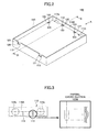
- FIG. 2 is a perspective view of a high frequency device of an embodiment of the present invention.
- a printed board 120 is fitted into a metal case 110. Opening parts 111a and 111b and notch parts 112 are formed in the case 110.
- the opening parts 111a and 111b are configured to connect a connector.
- the connector is configured to input and output a video signal.
- the notch parts 112 are configured to determine a position where the printed board 120 is fitted in the case 110.
- Various kinds of electronic circuits for performing as the high frequency device 100 are mounted on the printed board 120 (not illustrated in FIG. 2 ).
- claw parts 121 are formed at the printed board 120. By engaging the claw parts 121 with the notch parts 112, a position for fixing the printed board 120 is determined.
- a bottom plate and a lid part are provided at the case 110 so as to cover the printed board 120.
- Projecting parts 113 are formed at the case 110 of the embodiment of the present invention.
- the projecting parts 113 are configured to aid in soldering the printed board 120 and the case 110.
- two of the projecting parts 113 are provided between the opening part 111a and the opening part 111b.
- a single projecting part 113 is provided at each of two side plates perpendicular to a side plate 110A where the opening parts 111a and 111b are formed. Details of a structure of the projecting part 113 are discussed below.
- Concave parts 122 are formed at the printed board 120 of the embodiment of the present invention.
- the projecting parts 113 are engaged with the concave parts 122.
- the concave parts 122 are formed in positions where the projecting parts 113 are engaged when the printed board 120 is fixed to the case 110.
- a land part 123 is formed at the printed board 120 along a periphery of the concave part 122.
- the land part 123 may be formed so as to have, for example, a semicircular-shaped configuration or a configuration of half of an ellipse.
- the land part 123 may have a configuration where a head end of a semicircle is cut in a straight line manner (see FIG. 4(B) ).
- FIG. 3 is a side view of the high frequency device 100 seen in an A direction in FIG. 2 .
- the projecting part 113 may be formed by pressing the side plate 110A of the case 110 from an outside to an inside.
- the projecting part 113 has a bending configuration where the head projects inside to the side plate 110A.
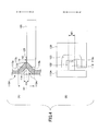
- FIG. 4(A) is a cross-sectional view taken along a line B-B of the high frequency device 100.
- FIG. 4(B) is a top view in a state where the projecting part 113 is engaged with the concave part 122.
- the projecting part 113 of the embodiment of the present invention has a bending configuration where a part of the side plate 110A is pressed to the inside of the case 110.
- an upper end part 113a and a lower end part 113b of the projecting part 113 are not separated from the side plate 110A.
- the projecting part 113 is formed so as to be continuous with the side plate 110A in a Y-Y direction.
- a solder guiding hole 114 is formed in a concave part 113A.
- the concave part 113A is formed at the external circumferential surface of the case 110.
- the solder guiding hole 114 is configured to guide the molten solder to the side of the case 110.
- the printed board 120 is provided so that the distance between the upper end part 113a and the land part 123 on the printed board 120 is H2.
- the distance H2 is approximately 1/2 of the width H1.
- the printed board 120 is provided so that a head end part 113c of the projecting part 113 is positioned on the same plane surface as the land part 123.
- the distance H2 is 1/2 of the width H1.
- the printed board 120 may be provided so that the land part 123 may be positioned in an area of a width H3 of the solder guiding hole 114 in the Y-Y direction.
- a width W1 in the X-X direction of the projecting part 113 of this embodiment is approximately 1 mm. See FIG. 4(B) .
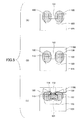
- FIGs. 5(A)-5(C) are views for explaining soldering of the case 110 and the printed board 120 of the embodiment of the present invention.
- cream solder 130 is applied on the land parts 123 of the printed board 120.
- the printed board 120 is inserted into the case 110 as shown in FIG. 5(B) .
- the projecting parts 113 formed at the case 110 are engaged with the corresponding concave parts 122 of the printed wiring board 120.
- the liquid solder flows in the space between the head end of the projecting part 113 and the concave part 122.
- the liquid solder goes to the external circumferential side of the case 110 due to capillarity generated by the solder guiding hole 114 formed at the projecting part 113, so as to flow into the concave part 113A formed at the external circumferential surface of the case 110.
- the capillarity is a phenomenon where liquid situated inside a narrow pipe may go up (against gravity) inside the pipe.
- the liquid solder comes together at a portion where the projecting part 113 and the land part 123 are connected to each other. At the same time, the flow of the liquid solder is spread to right and left uniformly at the internal circumferential surface of the side plate 110A of the case 110, so that a solder surface is formed.
- FIG. 6 is a view for explaining a state where the case 110 and the printed board 120 of the embodiment of the present invention are soldered.
- the concave part 113A of the projecting part 113 is filled with solder G so that the solder guiding hole 114 is blocked by the solder G.
- the printed board 120 and a part of the projecting part 113 situated above the surface of the printed board 120 where the land part 123 is formed, are connected to each other by the solder F having a large area.
- the case 110 and the printed board 120 can be fixed to each other with a large area.
- the part where the case 110 and the printed board 120 are connected to each other can have a stable solder configuration.
- the solder guiding hole 114 is blocked in the soldering step, it is possible to improve the shield effect of the case 110 so that good electric properties can be kept.
- the projecting part 113 is provided in the vicinity of a connector configured to input and output video signals, it is possible to reduce noise or the like of the video signals.
- no opening part is provided at the case 110 after the soldering is completed, it is possible to maintain the strength of the case 110.
- the liquid solder spontaneously spreads between the projecting part 113 and the land part 123 by the capillarity. Therefore, when the cream solder 130 is applied on the land 123, the cream solder may be applied in a position of the solder guiding hole 114. Because of this, in this embodiment, after the cream solder 130 is applied on the land part 123, the printed board 120 can be inserted in the case 110. Therefore, regardless of the configuration of the case 110, it is possible to apply the cream solder by a device having a simple structure.
- the act of guiding the solder to the case 110 of this embodiment is not performed.
- a device having a structure corresponding to the configuration of the case 110 is required. Therefore, large-sized equipment is required and flexibility of the equipment is degraded.
- the printed board 120 can be installed in the case 110. Therefore, it is possible to directly apply the cream solder to the printed board 120. Hence, the cream solder can be applied by simple equipment.
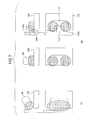
- FIGs. 7(A) and 7(B) are views for explaining application of cream solder.
- FIG. 7(A) is a view for explaining a related art structure where the solder guiding hole 114 is not provided.
- FIG. 7(B) is a view for explaining a structure where the solder guiding hole 114 is provided.
- a cream solder applying pipe 60 for applying the cream solder should have a configuration corresponding to the case.
- the printed board 120 and the case 110 can be stably soldered in a simple step in a reflow process and good electric capabilities (properties) can be obtained.
- FIG. 8 is a view showing a first modified example.
- FIG. 9 is a view showing a second modified example.
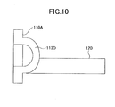
- FIG. 10 is a view showing a third modified example.
- a projecting part 113B does not have the bending configuration but a substantially square-shaped configuration.
- a solder guiding hole 114B is provided at the projecting part 113B shown in FIG. 8 .
- a projecting part 113C is bent at approximately 90 degrees.
- a solder guiding hole 114C is provided at the projecting part 113C shown in FIG. 9 .
- a projecting part 113D has a circular-shaped configuration.
- a solder guiding hole 114D is provided at a projecting part 113D shown in FIG. 10 .
- One aspect of the embodiments of the present invention may be to provide a high frequency device (100), including a metal case (110); a printed board (120) configured to be inserted in the case (110); a projecting part (113) configured to project to an inside of the case (110); a solder guiding hole (114) formed at the projecting part (113); a board concave part (122) formed in a position of the printed board (120), the position corresponding to the projecting part (113); and a land surface (123) formed on the printed board (120) along an edge of the board concave part (122), wherein the printed board (120) is provided so that a part of the solder guiding hole (114) is positioned above the land surface (123) when the printed board (120) is inserted in the case (110).
- the projecting part (113) may be formed so as to be continuous with a side plate in a long side direction or a short side direction of the side plate of the case (110) where the projecting part (113) is formed.
- An upper end part and a lower end part of the projecting part may not be separated from the side plate and the projecting part may be formed so as to be continuous with the side plate.
- the printed board (120) may be provided so that a head end (113c) of the projecting part (113) is positioned on a same plane surface as the land surface (123).
- a case concave part (113A) may be formed at an external circumferential surface of the projecting part (113) along a configuration of the projecting part (113).
- the projecting part (113) may have a bending configuration where a part of the side plate (110A) is pressed to the inside of the case (110).
- the solder guiding hole (114) may be configured to guide solder from an internal circumferential side to an external circumferential side of the case (110), the solder being configured to connect the case (110) and the printed board (120) to each other.
- Another aspect of the embodiments of the present invention may be to provide a printed board holding structure including a metal case (110) and a printed board (120) configured to be inserted in the case (110), the printed board holding structure being configured to hold the printed board (120), the printed board holding structure including: a projecting part (113) configured to project to an inside of the case (110); a solder guiding hole (114) formed at the projecting part (113); a board concave part (122) formed in a position of the printed board (120), the position corresponding to the projecting part (113); and a land surface (123) formed on the printed board (120) along an edge of the board concave part (122), wherein the printed board (120) is provided so that a part of the solder guiding hole (114) is positioned above the land surface (123) when the printed board (120) is inserted in the case (110).
Landscapes
- Engineering & Computer Science (AREA)
- Microelectronics & Electronic Packaging (AREA)
- Signal Processing (AREA)
- Shielding Devices Or Components To Electric Or Magnetic Fields (AREA)
- Mounting Of Printed Circuit Boards And The Like (AREA)
- Combinations Of Printed Boards (AREA)
Abstract
Description
- This patent application is based upon and claims the benefit of priority of Japanese Patent Application No.
2010-141223 filed on June 22, 2010 - The present invention generally relates to high frequency devices and printed board holding structures. More specifically, the present invention relates to a high frequency device and a printed board holding structure having a metal case, and a printed board configured to be inserted into the case.
- A structure, where a printed board having an electronic circuit mounted is inserted in and fixed to a metal case which also works as a shield plate, has been suggested as a high frequency device used for, for example, a television set. In such a high frequency device, the printed board and the case are soldered and fixed to each other by a reflow method using cream solder. With reference to
FIG. 1 , fixing of the printed board and the case in the related art high frequency device is discussed as follows.FIG. 1 is a view for explaining an example where a printed board and a case are fixed to each other. - It is normal practice, considering dimension error of each of the printed board and the case, to design so that a space of approximately 0.1 mm through approximately 0.2 mm between the printed board and the case is provided when the printed board is inserted in the case. When the printed board and the case are soldered, the space is filled with the solder so that the printed board and the case are fixed to each other.
-
FIG. 1(A) shows a state wherecream solder 3 is applied between acase 1 and a printedboard 2 in order to fill a space H between thecase 1 and the printedboard 2.FIG. 1(B) shows a state where the cream solder is melted by heating in the reflow process in the state shown inFIG. 1(A). FIG. 1(C) shows an ideal solder state when thecase 1 and the printedboard 2 are fixed to each other. - However, actually, in the state shown in
FIG. 1(B) where the solder is melted by the reflow process, unevenness in the spreading of the solder (solder configuration) to contact theheated case 1 is generated due to the difference of heat capacity between the space H and thecase 1 and the printedboard 2. Therefore, the state shown inFIG. 1(C) may not be formed. - In the related art, means reducing such unevenness are considered. For example, a frame and a printed board having the following structure have been suggested in Japanese Laid-Open Patent Application Publication No.
8-56085 - Japanese Laid-Open Patent Application Publication No.
11-121945 7-122874 - However, in techniques discussed in, for example, Japanese Laid-Open Patent Application Publication No.
8-56085 11-121945 7-122874 - Accordingly, embodiments of the present invention may provide a novel and useful high frequency device and a printed board holding structure solving one or more of the problems discussed above.
- More specifically, the embodiments of the present invention may provide a high frequency device and a printed board holding structure where a printed board and a case can be stably soldered in a simple step in a reflow process and good electric capabilities can be obtained.
- Another aspect of the embodiments of the present invention may be to provide a high frequency device, including a metal case; a printed board configured to be inserted in the case; a projecting part configured to project to an inside of the case; a solder guiding hole formed at the projecting part; a board concave part formed in a position of the printed board, the position corresponding to the projecting part; and a land surface formed on the printed board along an edge of the board concave part, wherein the printed board is provided so that a part of the solder guiding hole is positioned above the land surface when the printed board is inserted in the case.
- Another aspect of the embodiments of the present invention may be to provide a printed board holding structure including a metal case and a printed board configured to be inserted in the case, the printed board holding structure being configured to hold the printed board, the printed board holding structure including a projecting part configured to project to an inside of the case; a solder guiding hole formed at the projecting part; a board concave part formed in a position of the printed board, the position corresponding to the projecting part; and a land surface formed on the printed board along an edge of the board concave part, wherein the printed board is provided so that a part of the solder guiding hole is positioned above the land surface when the printed board is inserted in the case.
- Additional objects and advantages of the embodiments are set forth in part in the description which follows, and in part will become obvious from the description, or may be learned by practice of the invention. The object and advantages of the invention will be realized and attained by means of the elements and combinations particularly pointed out in the appended claims. It is to be understood that both the foregoing general description and the following detailed description are exemplary and explanatory and are not restrictive of the invention as claimed.
-
-
FIG. 1 is a view for explaining an example where a printed board and a case are fixed to each other; -
FIG. 2 is a perspective view of a high frequency device of an embodiment of the present invention; -
FIG. 3 is a side view of the high frequency device seen in an A direction inFIG. 2 ; -
FIG. 4 is a cross-sectional view taken along a line B-B and a top view of the high frequency device ofFIG. 2 ; -
FIG. 5 is a view for explaining soldering of the case and the printed board of the embodiment of the present invention; -
FIG. 6 is a view for explaining a state where the case and the printed board of the embodiment of the present invention are soldered; -
FIG. 7 is a view for explaining application of cream solder; -
FIG. 8 is a view showing a first modified example; -
FIG. 9 is a view showing a second modified example; and -
FIG. 10 is a view showing a third modified example. - A description is given below, with reference to the
FIG. 2 through FIG. 10 of embodiments of the present invention. - In the embodiments of the present invention, a projecting part is formed at a metal case. The projecting part is formed in a body with the case. The projecting part is configured to project to an inside of the case. A solder guiding hole is formed at a part of the projecting part. The solder is guided from the inside to the outside of the case by the solder guiding part. The projecting part is engaged with a concave part of the printed board and soldering is performed in a reflow process.
-
FIG. 2 is a perspective view of a high frequency device of an embodiment of the present invention. In ahigh frequency device 100 of the embodiment of the present invention, a printedboard 120 is fitted into ametal case 110.Opening parts notch parts 112 are formed in thecase 110. Theopening parts notch parts 112 are configured to determine a position where the printedboard 120 is fitted in thecase 110. Various kinds of electronic circuits for performing as thehigh frequency device 100 are mounted on the printed board 120 (not illustrated inFIG. 2 ). In addition, clawparts 121 are formed at the printedboard 120. By engaging theclaw parts 121 with thenotch parts 112, a position for fixing the printedboard 120 is determined. A bottom plate and a lid part are provided at thecase 110 so as to cover the printedboard 120. - Projecting
parts 113 are formed at thecase 110 of the embodiment of the present invention. The projectingparts 113 are configured to aid in soldering the printedboard 120 and thecase 110. At thecase 110 of the embodiment of the present invention, two of the projectingparts 113 are provided between theopening part 111a and theopening part 111b. A single projectingpart 113 is provided at each of two side plates perpendicular to aside plate 110A where the openingparts part 113 are discussed below. -
Concave parts 122 are formed at the printedboard 120 of the embodiment of the present invention. The projectingparts 113 are engaged with theconcave parts 122. Theconcave parts 122 are formed in positions where the projectingparts 113 are engaged when the printedboard 120 is fixed to thecase 110. Aland part 123 is formed at the printedboard 120 along a periphery of theconcave part 122. Theland part 123 may be formed so as to have, for example, a semicircular-shaped configuration or a configuration of half of an ellipse. Theland part 123 may have a configuration where a head end of a semicircle is cut in a straight line manner (seeFIG. 4(B) ). - Details of the projecting
part 113 of the embodiment of the present invention are further discussed.FIG. 3 is a side view of thehigh frequency device 100 seen in an A direction inFIG. 2 . In this embodiment, the projectingpart 113 may be formed by pressing theside plate 110A of thecase 110 from an outside to an inside. The projectingpart 113 has a bending configuration where the head projects inside to theside plate 110A. -
FIG. 4(A) is a cross-sectional view taken along a line B-B of thehigh frequency device 100.FIG. 4(B) is a top view in a state where the projectingpart 113 is engaged with theconcave part 122. - As shown in
FIG. 4(A) , the projectingpart 113 of the embodiment of the present invention has a bending configuration where a part of theside plate 110A is pressed to the inside of thecase 110. In addition, in this embodiment, anupper end part 113a and alower end part 113b of the projectingpart 113 are not separated from theside plate 110A. The projectingpart 113 is formed so as to be continuous with theside plate 110A in a Y-Y direction. - In this embodiment, by forming the projecting
part 113 configured to project to the inside of thecase 110, asolder guiding hole 114 is formed in aconcave part 113A. Theconcave part 113A is formed at the external circumferential surface of thecase 110. Thesolder guiding hole 114 is configured to guide the molten solder to the side of thecase 110. - Assuming that a width of the projecting
part 113 between theupper end part 113a and thelower end part 113b is defined as H1, the printedboard 120 is provided so that the distance between theupper end part 113a and theland part 123 on the printedboard 120 is H2. In this embodiment, the distance H2 is approximately 1/2 of the width H1. The printedboard 120 is provided so that ahead end part 113c of the projectingpart 113 is positioned on the same plane surface as theland part 123. - It may not be necessary that the distance H2 is 1/2 of the width H1. In this embodiment, the printed
board 120 may be provided so that theland part 123 may be positioned in an area of a width H3 of thesolder guiding hole 114 in the Y-Y direction. By this arrangement, when the cream solder applied on theland part 123 becomes liquid, it is possible to guide the liquid solder to thesolder guiding hole 114. Furthermore, a width W1 in the X-X direction of the projectingpart 113 of this embodiment is approximately 1 mm. SeeFIG. 4(B) . - Next, soldering of the
case 110 and the printedboard 120 of the embodiment of the present invention is discussed with reference toFIGs. 5(A)-5(C). FIGs. 5(A)-5(C) are views for explaining soldering of thecase 110 and the printedboard 120 of the embodiment of the present invention. - In this embodiment, first, in a step shown in
FIG. 5(A) ,cream solder 130 is applied on theland parts 123 of the printedboard 120. After thecream solder 130 is applied on theland parts 123, the printedboard 120 is inserted into thecase 110 as shown inFIG. 5(B) . At this time, the projectingparts 113 formed at thecase 110 are engaged with the correspondingconcave parts 122 of the printedwiring board 120. - In this state, when the printed
board 120 is engaged with thecase 110, heating is applied by a reflow process. By this heating, thecream solder 130 applied on theland part 123 is melted and becomes liquid so as to be spread into a solder configuration whereby thecase 110 and the printedboard 120 are fixed to each other. - Next, melting of the
cream solder 130 of this embodiment is discussed with reference toFIG. 5(C) . - By applying heat in the state shown in
FIG. 5(B) , the liquid solder flows in the space between the head end of the projectingpart 113 and theconcave part 122. As a result of this, the liquid solder goes to the external circumferential side of thecase 110 due to capillarity generated by thesolder guiding hole 114 formed at the projectingpart 113, so as to flow into theconcave part 113A formed at the external circumferential surface of thecase 110. The capillarity is a phenomenon where liquid situated inside a narrow pipe may go up (against gravity) inside the pipe. - By this flow of the solder, the liquid solder comes together at a portion where the projecting
part 113 and theland part 123 are connected to each other. At the same time, the flow of the liquid solder is spread to right and left uniformly at the internal circumferential surface of theside plate 110A of thecase 110, so that a solder surface is formed. - As a result of this, in this embodiment, a large area between the projecting
part 113 and theside plate 110A is covered with the solder. Thesolder guiding hole 114 is blocked with the guided solder. -
FIG. 6 is a view for explaining a state where thecase 110 and the printedboard 120 of the embodiment of the present invention are soldered. As shown inFIG. 6 , in this embodiment, theconcave part 113A of the projectingpart 113 is filled with solder G so that thesolder guiding hole 114 is blocked by the solder G. In addition, the printedboard 120 and a part of the projectingpart 113 situated above the surface of the printedboard 120 where theland part 123 is formed, are connected to each other by the solder F having a large area. - In this embodiment, with this structure, the
case 110 and the printedboard 120 can be fixed to each other with a large area. In addition, the part where thecase 110 and the printedboard 120 are connected to each other can have a stable solder configuration. Furthermore, in this embodiment, since thesolder guiding hole 114 is blocked in the soldering step, it is possible to improve the shield effect of thecase 110 so that good electric properties can be kept. In addition, in this embodiment, since the projectingpart 113 is provided in the vicinity of a connector configured to input and output video signals, it is possible to reduce noise or the like of the video signals. Furthermore, since no opening part is provided at thecase 110 after the soldering is completed, it is possible to maintain the strength of thecase 110. - In addition, in this embodiment, the liquid solder spontaneously spreads between the projecting
part 113 and theland part 123 by the capillarity. Therefore, when thecream solder 130 is applied on theland 123, the cream solder may be applied in a position of thesolder guiding hole 114. Because of this, in this embodiment, after thecream solder 130 is applied on theland part 123, the printedboard 120 can be inserted in thecase 110. Therefore, regardless of the configuration of thecase 110, it is possible to apply the cream solder by a device having a simple structure. - In a case where the above-discussed structure is not provided or a case of the related art structure, the act of guiding the solder to the
case 110 of this embodiment is not performed. In order to perform well the soldering of thecase 110, it is necessary to apply the cream solder to both the printedboard 120 and thecase 110 after the printedboard 120 is inserted into thecase 110. In this case, in order to apply the cream solder to the printedboard 120 having been installed in thecase 110, a device having a structure corresponding to the configuration of thecase 110 is required. Therefore, large-sized equipment is required and flexibility of the equipment is degraded. - On the other hand, in this embodiment, after the cream solder is applied to the printed
board 120, the printedboard 120 can be installed in thecase 110. Therefore, it is possible to directly apply the cream solder to the printedboard 120. Hence, the cream solder can be applied by simple equipment. -
FIGs. 7(A) and 7(B) are views for explaining application of cream solder.FIG. 7(A) is a view for explaining a related art structure where thesolder guiding hole 114 is not provided.FIG. 7(B) is a view for explaining a structure where thesolder guiding hole 114 is provided. - As shown in
FIG. 7(A) , in a situation where thesolder guiding hole 114 is not provided, the cream solder is applied to both the printedboard 120 and the case in the state where the printedboard 120 is inserted into the case. In this situation, a creamsolder applying pipe 60 for applying the cream solder should have a configuration corresponding to the case. - On the other hand, as shown in
FIG. 7(B) , in the case of this embodiment where thesolder guiding hole 114 is provided, after the cream solder is applied to the printedboard 120, the printedboard 120 is inserted into thecase 110. Therefore, it is not necessary for the configuration of the creamsolder applying pipe 60 to correspond to the configuration of thecase 110. Hence, it is possible to apply the cream solder by using the cream solder applying pipe having high flexibility. - According to the embodiments of the present invention, the printed
board 120 and thecase 110 can be stably soldered in a simple step in a reflow process and good electric capabilities (properties) can be obtained. - Modified examples of the embodiment of the present invention are discussed with reference to
FIG. 8 through FIG. 10 .FIG. 8 is a view showing a first modified example.FIG. 9 is a view showing a second modified example.FIG. 10 is a view showing a third modified example. - In the example shown in
FIG. 8 , a projectingpart 113B does not have the bending configuration but a substantially square-shaped configuration. Asolder guiding hole 114B is provided at the projectingpart 113B shown inFIG. 8 . - In the example shown in
FIG. 9 , a projectingpart 113C is bent at approximately 90 degrees. Asolder guiding hole 114C is provided at the projectingpart 113C shown inFIG. 9 . - In the example shown in
FIG. 10 , a projectingpart 113D has a circular-shaped configuration. A solder guiding hole 114D is provided at a projectingpart 113D shown inFIG. 10 . - All examples and conditional language recited herein are intended for pedagogical purposes to aid the reader in understanding the invention and the concepts contributed by the inventor to furthering the art, and are to be construed as being without limitation to such specifically recited examples and conditions, nor does the organization of such examples in the specification relate to a showing of the superiority or inferiority of the invention. Although the embodiments of the present invention have been described in detail, it should be understood that the various changes, substitutions, and alterations could be made hereto without departing from the spirit and scope of the invention.
- Thus, according to the above-discussed embodiment of the present invention, the following high frequency device and printed board holding structure can be provided. In the following explanation, the numerical references are just for reference and therefore a scope of claims mentioned below is not limited by these numerical references.
- One aspect of the embodiments of the present invention may be to provide a high frequency device (100), including a metal case (110); a printed board (120) configured to be inserted in the case (110); a projecting part (113) configured to project to an inside of the case (110); a solder guiding hole (114) formed at the projecting part (113); a board concave part (122) formed in a position of the printed board (120), the position corresponding to the projecting part (113); and a land surface (123) formed on the printed board (120) along an edge of the board concave part (122), wherein the printed board (120) is provided so that a part of the solder guiding hole (114) is positioned above the land surface (123) when the printed board (120) is inserted in the case (110).
- The projecting part (113) may be formed so as to be continuous with a side plate in a long side direction or a short side direction of the side plate of the case (110) where the projecting part (113) is formed.
- An upper end part and a lower end part of the projecting part may not be separated from the side plate and the projecting part may be formed so as to be continuous with the side plate.
- The printed board (120) may be provided so that a head end (113c) of the projecting part (113) is positioned on a same plane surface as the land surface (123).
- A case concave part (113A) may be formed at an external circumferential surface of the projecting part (113) along a configuration of the projecting part (113).
- The projecting part (113) may have a bending configuration where a part of the side plate (110A) is pressed to the inside of the case (110).
- The solder guiding hole (114) may be configured to guide solder from an internal circumferential side to an external circumferential side of the case (110), the solder being configured to connect the case (110) and the printed board (120) to each other.
- Another aspect of the embodiments of the present invention may be to provide a printed board holding structure including a metal case (110) and a printed board (120) configured to be inserted in the case (110), the printed board holding structure being configured to hold the printed board (120), the printed board holding structure including: a projecting part (113) configured to project to an inside of the case (110); a solder guiding hole (114) formed at the projecting part (113); a board concave part (122) formed in a position of the printed board (120), the position corresponding to the projecting part (113); and a land surface (123) formed on the printed board (120) along an edge of the board concave part (122), wherein the printed board (120) is provided so that a part of the solder guiding hole (114) is positioned above the land surface (123) when the printed board (120) is inserted in the case (110).
- According to the embodiments of the present invention, it is possible to provide a high frequency device and a printed board holding structure where a printed board and a case can be stably soldered in a simple step in a reflow process and good electric capabilities can be obtained.
Claims (8)
- A high frequency device, comprising:a metal case;a printed board configured to be inserted in the case;a projecting part configured to project to an inside of the case;a solder guiding hole formed at the projecting part;a board concave part formed in a position of the printed board, the position corresponding to the projecting part; anda land surface formed on the printed board along an edge of the board concave part,wherein the printed board is provided so that a part of the solder guiding hole is positioned above the land surface when the printed board is inserted in the case.
- The high frequency device as claimed in claim 1,
wherein the projecting part is formed so as to be continuous with a side plate in a long side direction or a short side direction of the side plate of the case where the projecting part is formed. - The high frequency device as claimed in claim 1,
wherein an upper end part and a lower end part of the projecting part are not separated from the side plate and the projecting part is formed so as to be continuous with the side plate. - The high frequency device as claimed in claim 1,
wherein the printed board is provided so that a head end of the projecting part is positioned on a same plane surface as the land surface. - The high frequency device as claimed in claim 1,
wherein a case concave part is formed at an external circumferential surface of the projecting part along a configuration of the projecting part. - The high frequency device as claimed in claim 1,
wherein the projecting part has a bending configuration where a part of the side plate is pressed to the inside of the case. - The high frequency device as claimed in claim 1,
wherein the solder guiding hole is configured to guide solder from an internal circumferential side to an external circumferential side of the case, the solder being configured to connect the case and the printed board to each other. - A printed board holding structure including a metal case and a printed board configured to be inserted in the case, the printed board holding structure being configured to hold the printed board, the printed board holding structure comprising:a projecting part configured to project to an inside of the case;a solder guiding hole formed at the projecting part;a board concave part formed in a position of the printed board, the position corresponding to the projecting part; anda land surface formed on the printed board along an edge of the board concave part,wherein the printed board is provided so that a part of the solder guiding hole is positioned above the land surface when the printed board is inserted in the case.
Applications Claiming Priority (1)
| Application Number | Priority Date | Filing Date | Title |
|---|---|---|---|
| JP2010141223A JP2012009471A (en) | 2010-06-22 | 2010-06-22 | High-frequency device and printed board holding structure |
Publications (2)
| Publication Number | Publication Date |
|---|---|
| EP2400829A2 true EP2400829A2 (en) | 2011-12-28 |
| EP2400829A3 EP2400829A3 (en) | 2012-07-25 |
Family
ID=44673965
Family Applications (1)
| Application Number | Title | Priority Date | Filing Date |
|---|---|---|---|
| EP11168945A Withdrawn EP2400829A3 (en) | 2010-06-22 | 2011-06-07 | High frequency device and a printed board holding structure. |
Country Status (4)
| Country | Link |
|---|---|
| US (1) | US20110310573A1 (en) |
| EP (1) | EP2400829A3 (en) |
| JP (1) | JP2012009471A (en) |
| CN (1) | CN102300447A (en) |
Families Citing this family (3)
| Publication number | Priority date | Publication date | Assignee | Title |
|---|---|---|---|---|
| CN104750217A (en) * | 2013-12-31 | 2015-07-01 | 鸿富锦精密工业(武汉)有限公司 | Power supply |
| WO2017176521A1 (en) * | 2016-04-04 | 2017-10-12 | Commscope Technologies Llc | Systems and methods for thermal management for high power density emi shielded electronic devices |
| CN113597160B (en) * | 2021-07-22 | 2022-12-27 | 业成科技(成都)有限公司 | Shell frame and electronic equipment |
Citations (4)
| Publication number | Priority date | Publication date | Assignee | Title |
|---|---|---|---|---|
| JPH07122874A (en) | 1993-10-27 | 1995-05-12 | Matsushita Electric Ind Co Ltd | High frequency equipment |
| JPH0856085A (en) | 1994-08-11 | 1996-02-27 | Alps Electric Co Ltd | Printed board holding structure |
| JPH11121945A (en) | 1997-10-14 | 1999-04-30 | Alps Electric Co Ltd | Electronic apparatus and manufacture of the electronic apparatus |
| JP2010141223A (en) | 2008-12-15 | 2010-06-24 | Hitachi Kokusai Electric Inc | Method of manufacturing semiconductor device and substrate processing apparatus |
Family Cites Families (5)
| Publication number | Priority date | Publication date | Assignee | Title |
|---|---|---|---|---|
| JPS60124088A (en) * | 1983-12-09 | 1985-07-02 | Columbia Magune Prod Kk | Automatic cassette tape winding and assembling device |
| JPS60124088U (en) * | 1984-01-30 | 1985-08-21 | 関西日本電気株式会社 | printed wiring device |
| JPH10107463A (en) * | 1996-10-02 | 1998-04-24 | Alps Electric Co Ltd | Attaching structure of printed substrate |
| JP3267521B2 (en) * | 1996-11-08 | 2002-03-18 | アルプス電気株式会社 | PCB mounting structure |
| JP2001251070A (en) * | 2000-03-03 | 2001-09-14 | Sharp Corp | Board mounting structure |
-
2010
- 2010-06-22 JP JP2010141223A patent/JP2012009471A/en active Pending
-
2011
- 2011-05-26 US US13/116,354 patent/US20110310573A1/en not_active Abandoned
- 2011-06-07 EP EP11168945A patent/EP2400829A3/en not_active Withdrawn
- 2011-06-20 CN CN201110175609A patent/CN102300447A/en active Pending
Patent Citations (4)
| Publication number | Priority date | Publication date | Assignee | Title |
|---|---|---|---|---|
| JPH07122874A (en) | 1993-10-27 | 1995-05-12 | Matsushita Electric Ind Co Ltd | High frequency equipment |
| JPH0856085A (en) | 1994-08-11 | 1996-02-27 | Alps Electric Co Ltd | Printed board holding structure |
| JPH11121945A (en) | 1997-10-14 | 1999-04-30 | Alps Electric Co Ltd | Electronic apparatus and manufacture of the electronic apparatus |
| JP2010141223A (en) | 2008-12-15 | 2010-06-24 | Hitachi Kokusai Electric Inc | Method of manufacturing semiconductor device and substrate processing apparatus |
Also Published As
| Publication number | Publication date |
|---|---|
| US20110310573A1 (en) | 2011-12-22 |
| EP2400829A3 (en) | 2012-07-25 |
| JP2012009471A (en) | 2012-01-12 |
| CN102300447A (en) | 2011-12-28 |
Similar Documents
| Publication | Publication Date | Title |
|---|---|---|
| US9510438B2 (en) | Electronic control device | |
| JP3184248U (en) | Electronic circuit module cover structure | |
| JP2014093415A (en) | Electronic control device | |
| KR20080070495A (en) | Electromagnetic Interference Blocker and Manufacturing Method Thereof | |
| US20160192515A1 (en) | Circuit board assembly and assembling method thereof | |
| JP2022510118A (en) | Receptacle connector | |
| KR101011918B1 (en) | Cable assembly | |
| US20110310573A1 (en) | High frequency device and a printed board holding structure | |
| KR20140144405A (en) | Shield can assembly and electronic device having it | |
| CN210576836U (en) | A shielding case, shielding component and connector | |
| US11089703B2 (en) | Power converter | |
| KR20150060845A (en) | Module | |
| JP2016129210A (en) | Electronic device | |
| US9433092B2 (en) | Layout method for printed circuit board and printed circuit board thereof | |
| CN113709966B (en) | Printed circuit board assemblies and electronic equipment | |
| US9134077B2 (en) | Heat sink assembly with connecting member protruding from heat sink | |
| JP2011151051A (en) | Lsi package and method of manufacturing the same | |
| KR20080067914A (en) | Ferrite Core and Electromagnetic Noise Shielding Structure Having Same | |
| EP3089566A1 (en) | Electronic component | |
| JP2012221992A (en) | Electronic component package | |
| JP6890235B2 (en) | Circuit board manufacturing method, circuit board, and cover member | |
| JP2008198572A (en) | Electronic equipment | |
| US20260075715A1 (en) | Power module and auxiliary supporting device adapted thereto | |
| US9414492B2 (en) | Printed wiring board and electric tool switch provided therewith | |
| CN104715908B (en) | Flat surface transformer and electric component |
Legal Events
| Date | Code | Title | Description |
|---|---|---|---|
| AK | Designated contracting states |
Kind code of ref document: A2 Designated state(s): AL AT BE BG CH CY CZ DE DK EE ES FI FR GB GR HR HU IE IS IT LI LT LU LV MC MK MT NL NO PL PT RO RS SE SI SK SM TR |
|
| AX | Request for extension of the european patent |
Extension state: BA ME |
|
| PUAI | Public reference made under article 153(3) epc to a published international application that has entered the european phase |
Free format text: ORIGINAL CODE: 0009012 |
|
| PUAL | Search report despatched |
Free format text: ORIGINAL CODE: 0009013 |
|
| AK | Designated contracting states |
Kind code of ref document: A3 Designated state(s): AL AT BE BG CH CY CZ DE DK EE ES FI FR GB GR HR HU IE IS IT LI LT LU LV MC MK MT NL NO PL PT RO RS SE SI SK SM TR |
|
| AX | Request for extension of the european patent |
Extension state: BA ME |
|
| RIC1 | Information provided on ipc code assigned before grant |
Ipc: H05K 9/00 20060101AFI20120619BHEP Ipc: H05K 7/14 20060101ALI20120619BHEP |
|
| STAA | Information on the status of an ep patent application or granted ep patent |
Free format text: STATUS: THE APPLICATION IS DEEMED TO BE WITHDRAWN |
|
| 18D | Application deemed to be withdrawn |
Effective date: 20130126 |