EP2400562B1 - Verbindungseinrichtung anordenbar zu einem Photovoltaikmodul - Google Patents
Verbindungseinrichtung anordenbar zu einem Photovoltaikmodul Download PDFInfo
- Publication number
- EP2400562B1 EP2400562B1 EP11166658.2A EP11166658A EP2400562B1 EP 2400562 B1 EP2400562 B1 EP 2400562B1 EP 11166658 A EP11166658 A EP 11166658A EP 2400562 B1 EP2400562 B1 EP 2400562B1
- Authority
- EP
- European Patent Office
- Prior art keywords
- devices
- connection
- contact
- housing element
- circuit arrangement
- Prior art date
- Legal status (The legal status is an assumption and is not a legal conclusion. Google has not performed a legal analysis and makes no representation as to the accuracy of the status listed.)
- Not-in-force
Links
- 239000004065 semiconductor Substances 0.000 claims description 46
- 238000001816 cooling Methods 0.000 claims description 10
- 239000000758 substrate Substances 0.000 claims description 8
- 239000004020 conductor Substances 0.000 description 9
- 229910052751 metal Inorganic materials 0.000 description 5
- 239000002184 metal Substances 0.000 description 5
- 238000010586 diagram Methods 0.000 description 4
- 230000007613 environmental effect Effects 0.000 description 4
- 238000010292 electrical insulation Methods 0.000 description 2
- 230000002441 reversible effect Effects 0.000 description 2
- RYGMFSIKBFXOCR-UHFFFAOYSA-N Copper Chemical group [Cu] RYGMFSIKBFXOCR-UHFFFAOYSA-N 0.000 description 1
- 229910052782 aluminium Inorganic materials 0.000 description 1
- XAGFODPZIPBFFR-UHFFFAOYSA-N aluminium Chemical class [Al] XAGFODPZIPBFFR-UHFFFAOYSA-N 0.000 description 1
- 239000002131 composite material Substances 0.000 description 1
- 150000001875 compounds Chemical class 0.000 description 1
- 229910052802 copper Inorganic materials 0.000 description 1
- 239000010949 copper Substances 0.000 description 1
- 230000007547 defect Effects 0.000 description 1
- 230000001419 dependent effect Effects 0.000 description 1
- 230000005611 electricity Effects 0.000 description 1
- 239000011888 foil Substances 0.000 description 1
- 238000011990 functional testing Methods 0.000 description 1
- 230000017525 heat dissipation Effects 0.000 description 1
- 239000011810 insulating material Substances 0.000 description 1
- 239000000463 material Substances 0.000 description 1
- 239000007769 metal material Substances 0.000 description 1
- 238000004382 potting Methods 0.000 description 1
- 238000007789 sealing Methods 0.000 description 1
- 229920002379 silicone rubber Polymers 0.000 description 1
- 239000004945 silicone rubber Substances 0.000 description 1
- 230000008646 thermal stress Effects 0.000 description 1
Images

Classifications
-
- H—ELECTRICITY
- H01—ELECTRIC ELEMENTS
- H01L—SEMICONDUCTOR DEVICES NOT COVERED BY CLASS H10
- H01L31/00—Semiconductor devices sensitive to infrared radiation, light, electromagnetic radiation of shorter wavelength or corpuscular radiation and specially adapted either for the conversion of the energy of such radiation into electrical energy or for the control of electrical energy by such radiation; Processes or apparatus specially adapted for the manufacture or treatment thereof or of parts thereof; Details thereof
- H01L31/04—Semiconductor devices sensitive to infrared radiation, light, electromagnetic radiation of shorter wavelength or corpuscular radiation and specially adapted either for the conversion of the energy of such radiation into electrical energy or for the control of electrical energy by such radiation; Processes or apparatus specially adapted for the manufacture or treatment thereof or of parts thereof; Details thereof adapted as photovoltaic [PV] conversion devices
- H01L31/042—PV modules or arrays of single PV cells
- H01L31/05—Electrical interconnection means between PV cells inside the PV module, e.g. series connection of PV cells
-
- H—ELECTRICITY
- H01—ELECTRIC ELEMENTS
- H01L—SEMICONDUCTOR DEVICES NOT COVERED BY CLASS H10
- H01L31/00—Semiconductor devices sensitive to infrared radiation, light, electromagnetic radiation of shorter wavelength or corpuscular radiation and specially adapted either for the conversion of the energy of such radiation into electrical energy or for the control of electrical energy by such radiation; Processes or apparatus specially adapted for the manufacture or treatment thereof or of parts thereof; Details thereof
- H01L31/04—Semiconductor devices sensitive to infrared radiation, light, electromagnetic radiation of shorter wavelength or corpuscular radiation and specially adapted either for the conversion of the energy of such radiation into electrical energy or for the control of electrical energy by such radiation; Processes or apparatus specially adapted for the manufacture or treatment thereof or of parts thereof; Details thereof adapted as photovoltaic [PV] conversion devices
- H01L31/042—PV modules or arrays of single PV cells
- H01L31/044—PV modules or arrays of single PV cells including bypass diodes
-
- H—ELECTRICITY
- H02—GENERATION; CONVERSION OR DISTRIBUTION OF ELECTRIC POWER
- H02G—INSTALLATION OF ELECTRIC CABLES OR LINES, OR OF COMBINED OPTICAL AND ELECTRIC CABLES OR LINES
- H02G3/00—Installations of electric cables or lines or protective tubing therefor in or on buildings, equivalent structures or vehicles
- H02G3/02—Details
- H02G3/08—Distribution boxes; Connection or junction boxes
-
- H—ELECTRICITY
- H02—GENERATION; CONVERSION OR DISTRIBUTION OF ELECTRIC POWER
- H02S—GENERATION OF ELECTRIC POWER BY CONVERSION OF INFRARED RADIATION, VISIBLE LIGHT OR ULTRAVIOLET LIGHT, e.g. USING PHOTOVOLTAIC [PV] MODULES
- H02S40/00—Components or accessories in combination with PV modules, not provided for in groups H02S10/00 - H02S30/00
- H02S40/30—Electrical components
- H02S40/34—Electrical components comprising specially adapted electrical connection means to be structurally associated with the PV module, e.g. junction boxes
- H02S40/345—Electrical components comprising specially adapted electrical connection means to be structurally associated with the PV module, e.g. junction boxes with cooling means associated with the electrical connection means, e.g. cooling means associated with or applied to the junction box
-
- H—ELECTRICITY
- H02—GENERATION; CONVERSION OR DISTRIBUTION OF ELECTRIC POWER
- H02S—GENERATION OF ELECTRIC POWER BY CONVERSION OF INFRARED RADIATION, VISIBLE LIGHT OR ULTRAVIOLET LIGHT, e.g. USING PHOTOVOLTAIC [PV] MODULES
- H02S40/00—Components or accessories in combination with PV modules, not provided for in groups H02S10/00 - H02S30/00
- H02S40/30—Electrical components
- H02S40/36—Electrical components characterised by special electrical interconnection means between two or more PV modules, e.g. electrical module-to-module connection
-
- H—ELECTRICITY
- H05—ELECTRIC TECHNIQUES NOT OTHERWISE PROVIDED FOR
- H05K—PRINTED CIRCUITS; CASINGS OR CONSTRUCTIONAL DETAILS OF ELECTRIC APPARATUS; MANUFACTURE OF ASSEMBLAGES OF ELECTRICAL COMPONENTS
- H05K7/00—Constructional details common to different types of electric apparatus
- H05K7/20—Modifications to facilitate cooling, ventilating, or heating
-
- Y—GENERAL TAGGING OF NEW TECHNOLOGICAL DEVELOPMENTS; GENERAL TAGGING OF CROSS-SECTIONAL TECHNOLOGIES SPANNING OVER SEVERAL SECTIONS OF THE IPC; TECHNICAL SUBJECTS COVERED BY FORMER USPC CROSS-REFERENCE ART COLLECTIONS [XRACs] AND DIGESTS
- Y02—TECHNOLOGIES OR APPLICATIONS FOR MITIGATION OR ADAPTATION AGAINST CLIMATE CHANGE
- Y02E—REDUCTION OF GREENHOUSE GAS [GHG] EMISSIONS, RELATED TO ENERGY GENERATION, TRANSMISSION OR DISTRIBUTION
- Y02E10/00—Energy generation through renewable energy sources
- Y02E10/50—Photovoltaic [PV] energy
Definitions
- connection device also known as a junction box.
- connection devices are usually arranged directly on a photovoltaic module and serve for the electrical connection to further photovoltaic modules and also for the electrical connection to an inverter device.
- the individual photovoltaic modules are connected in series and with the inverter device, for which purpose the connecting device still has one, usually designed as bypass diodes, semiconductor circuit arrangement.
- This semiconductor device can also have a plurality of series-connected bypass diodes, depending on the internal interconnection of the photovoltaic module.
- This semiconductor device thus usually has the task in the event of a fault of the associated photovoltaic module to bridge this and to ensure the flow of current in the entire photovoltaic system.
- a connecting device which, by way of example, is disclosed in relation to others DE 10 2007 020 846 A1 or the DE 10 2008 022 056 A1 , has a metal housing.
- This metal housing improves the cooling of the semiconductor devices in the interior of the connecting device by these are arranged close to the edges of the side edges.
- first connection means for connection to the photovoltaic module and second connection means for connection within the photovoltaic system known.
- Also well known from this semiconductor components are primarily in the function of bypass diodes, which are connected circuit-wise with the connection devices.
- the invention has for its object to present a connection device for arrangement to a photovoltaic module, wherein the entirety of the semiconductor devices a functional test, without photovoltaic module, accessible, at the same time in the operation of efficient cooling is accessible and also in the event of an error with little effort is replaceable.
- connection device can be arranged to a photovoltaic module for electrically connecting a plurality of photovoltaic modules with each other and / or with an inverter device, as are common in a series connection of the photovoltaic modules.
- the connecting device has a housing which consists of at least, preferably exactly two sub-housings and has first and second connection devices.
- the first housing part is arranged directly on the photovoltaic module, typically on the rear side thereof, and connected in a materially bonded manner.
- the photovoltaic module go out at least two, often more, direct current connection cable or gleichflachleiter, which are electrically conductively connected to first connection means of the connecting device.
- the implementation of these cables or flat conductors is carried out according to the prior art after necessary protection against moisture and with necessary electrical insulation.
- the materials plastic, as well as metal or mixed forms by way of example with a first part of plastic body and a second part of metal body, as embodiments of the housing available.
- the first connection devices are in this case arranged in the first part housing.
- the second connection devices for the serial connection of the photovoltaic module are also arranged in the first sub-housing via the connection device within the photovoltaic system. This creates a Connection unit for complete external electrical connection of the connection device.
- a semiconductor circuit arrangement is arranged as a functional unit which comprises all semiconductor components as well as their complete interconnection device.
- a semiconductor unit results from the second housing part and the semiconductor circuit arrangement, which as such is accessible to a complete electrical test.
- This semiconductor circuit arrangement is configured with preferably only one electrically insulating substrate and conductor tracks formed thereon. On these interconnects, the semiconductor components of the semiconductor circuit arrangement are arranged as unhoused component and connected in accordance with the circuit. For electrical insulation as well as for heat dissipation of the resulting heat loss, the semiconductor circuit arrangement is covered with a potting compound.
- the semiconductor component may be formed as higgested components and to arrange it in a force-locking manner in respective pressure contact devices connected in a manner suitable for the circuit.
- a recess is provided in the first part body, which extends through the one cooling device from the interior of the housing and wherein in this case this recess is of course sealed sufficiently against environmental influences.
- the second part body also has second contact devices which connect the circuit arrangement to the connection devices of the first part body, which have first contact devices for this purpose, in an electrically conductive manner.
- These contact devices are advantageously designed as plug-in or spring contacts.
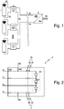
- Fig. 1 schematically shows a photovoltaic system with a plurality of photovoltaic modules (1) with each of these photovoltaic modules (1) associated inventive connecting device (2). It is preferable to arrange this respective connecting device (2) directly on the rear side of the photovoltaic module (1) and to connect it electrically conductively to its DC connecting cable or flat conductor (10, 12).
- the photovoltaic modules (1) are connected in series with one another by means of the associated connection devices (2) and with an inverter device (6) via respective connection cables (60, 62, 64).
- this inverter device (6) By means of this inverter device (6), the direct current generated in the photovoltaic modules (1) is converted into alternating current and fed into a power grid (66).
- the connecting device (2) is not used here not only the said electrical connection but also the bridging of individual photovoltaic modules (1) in case of failure. In this case of error, the photovoltaic module (1) delivers no electricity and also has no conductivity.
- the connecting devices (2) have a semiconductor circuit arrangement (cf. Fig. 2 , 50), which can act at least as a bypass.
- Fig. 2 shows a schematic diagram of a connecting device (2) according to the invention with a two partial housings (20, 40) existing housing (3).
- this often has more than the two required DC connecting cables or flat conductors (10, 12).
- first connection devices (100) arranged in the first sub-housing are furthermore connected to first contact devices (32) likewise arranged in the first sub-housing (20), which are each in contactable with associated second contact devices (34) of the second sub-housing (40).
- the semiconductor circuit arrangement (50) is provided and consists of three diodes (500), which has a bypass function for the photovoltaic module (see. Fig. 1, 1st ) train.
- the second connection devices (600) for connection to further connection devices (2) or the inverter device (6) are likewise preferably arranged in the first part housing (20). In principle, however, an arrangement in the second sub-housing (40) is possible, although not preferred.
- Fig. 3 shows a schematic diagram of a connecting device (2) arranged directly on the back of a photovoltaic module (1). From this photovoltaic module (1) lead direct current connection cable (10, 12) in the connecting device (2), in which case, of course, a necessary protection of the interior of the connecting device is provided against environmental influences. These DC connection cables are connected to first connection devices (100). Also shown are second connection means (600), as well as the associated cables (60, 62, 64) of the serial connection within the photovoltaic system. These first and second connection devices (100, 600) are respectively arranged in the first part body (20) of the housing (3) of the connection device (2) and thus form their connection unit.
- the semiconductor circuit arrangement (50) is arranged, whereby the semiconductor unit is formed.
- the semiconductor circuit arrangement (50) consists of a plurality of pressure contact devices (502) which are connected directly, possibly in an electrically isolated manner, to the second sub-housing (40).
- these pressure contact devices (502) gehauste semiconductor devices (500), preferably power diodes, arranged and non-positively connected.
- the pressure contact devices (502) each have a receptacle (504) and a pressure element (506) with a resilient portion for this purpose.
- the second sub-housing (40) is formed from an insulating, sufficiently thermally conductive plastic and has at its the semiconductor circuit arrangement (50) or parts thereof, immediately adjacent, outside a plurality of cooling means (420). In the simplest embodiment, these are formed in one piece from the second part body (40) itself. It can at higher thermal stress, the second part of housing (40) form of a metallic material. Alternatively, it may also be preferable to make the outer wall of a plastic housing thinner in the designated area (426) and to provide a metallic heat sink (424) on the outside, as in FIG Fig. 3a shown.
- first (32) and associated second contact devices (34) are provided for electrically connecting the semiconductor circuit arrangement (50) of the second part body (40) to the first and second connection devices (100, 600) of the first part body (20).
- the respective first contact device (32) is in this case arranged in the first part body (20), while the respectively associated second contact devices (34) are arranged in the second part body (40).
- These respective contact devices (32, 34) are formed in this embodiment of the connecting device as a connector (320, 340) and shoot the respective contact between the first (32) and associated second contact means (34) in the arrangement of the first (20) to the second Part body (40).
- the first sub-body (20) with its connection devices (100, 600) arranged on the back of the photovoltaic module (1) and the entire photovoltaic system are completely electrically connected without the semiconductor circuit arrangement (50) itself must be present.
- the semiconductor circuit arrangement (50), as part of the semiconductor unit can be subjected to electrical tests independently of the connection unit.
- the semiconductor unit can be easily replaced in the event of a fault without having to disassemble the connections (60, 62, 64) of the photovoltaic system only partially.
- Fig. 4 shows a schematic diagram of an embodiment of a connecting device (2) according to the invention.
- the first part body (20) of the housing (3) differs from that according to FIG Fig. 3 in that here DC flat conductors (10, 12) are provided as part of the photovoltaic module (1) and these on the photovoltaic module (1) facing side of the connecting device (2) into this to lead.
- DC flat conductors (10, 12) are provided as part of the photovoltaic module (1) and these on the photovoltaic module (1) facing side of the connecting device (2) into this to lead.
- this also provides a necessary protection against environmental influences.
- second contact means (34) connectable with first contact means (32), in this case receptacles (322) are provided which ensure a secure contact with a contact spring (342) as a second contact means.
- the second sub-housing (40) here has an opening (44) which is provided to arrange a cooling device (52) in the form of a heat sink associated with the semiconductor circuit arrangement (50) and to seal it against environmental influences by means of a sealing device (520). It is preferred here and due to the thermal load usually sufficient if the cooling device (52) is a passive cooling device in the form of an aluminum heat sink. For special applications, however, an active cooling device, for example equipped with an additional fan, may also be preferred.
- the semiconductor circuit arrangement (50) is provided on this heat sink (52) facing the interior of the housing (3).
- This consists of a counter to the heat sink (52) electrically insulated but thermally very well conductive substrate (54).
- so-called DCB (direct copper bonded) substrates are particularly advantageous, but depending on the thermal conductivity requirement, IMS substrates or simple printed circuit boards are also suitable.
- the substrate (54) basically has a plurality of conductor tracks (542) with preferably unhoused semiconductor components (500) which are connected to one another in a circuit-compatible manner, for example by means of wire bonding connections or by means of a flexible conductor structure.
- uncaused semiconductor devices (500) it is furthermore particularly preferred to cover these with an insulating material, not shown, such as silicone rubber, for example
- contact springs (342) are provided in this embodiment, which are preferably held by means of holding means (46, 460) which are formed in one or more pieces with the second part housing (40) in this.
- the contact spring (342) are pressurized and form with the first contact elements (32), the receptacles (322) in the first housing part (20) from a safe but completely reversible electrical connection.
- the first part housing (20) necessary abutment (200) for generating a back pressure for this spring contact (302) is provided.
- first and second contact devices 32, 34
- first and second contact devices 32, 34
- a contact spring as first contact device
- an associated receptacle as second contact device
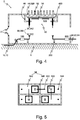
- Fig. 5 shows a semiconductor circuit arrangement (50) of a connecting device (3) according to the invention. Shown is a substrate (54) with a Isolierstoffgrundève (540) and arranged thereon interconnects (542), wherein on each conductor cohesively a semiconductor device (500), here a power diode and a contact surface (544) for the contact spring (see. Fig. 4 , 342) are arranged. Furthermore, the circuit-compatible connection (502) of the power diodes (500) is shown schematically, which can be formed in a very simple way by way of example by means of a film composite of an insulating film and a metal foil, which is structured in this case. Likewise, this circuit-compatible connection can be done by means of bonding wires.
Landscapes
- Engineering & Computer Science (AREA)
- Physics & Mathematics (AREA)
- Microelectronics & Electronic Packaging (AREA)
- Electromagnetism (AREA)
- Condensed Matter Physics & Semiconductors (AREA)
- General Physics & Mathematics (AREA)
- Computer Hardware Design (AREA)
- Power Engineering (AREA)
- Life Sciences & Earth Sciences (AREA)
- Sustainable Development (AREA)
- Structural Engineering (AREA)
- Civil Engineering (AREA)
- Architecture (AREA)
- Thermal Sciences (AREA)
- Photovoltaic Devices (AREA)
Description
- Die Erfindung beschreibt eine Verbindungseinrichtung, auch bekannt als Junction Box, Derartige Verbindungseinrichtungen sind üblicherweise direkt an einem Photovoltaikmodul angeordnet und dienen der elektrischen Verbindung zu weiteren Photovoltaikmodulen und auch der elektrischen Verbindung zu einer Wechselrichtereinrichtung. Üblicherweise sind in einer Photovoltaikanlage die einzelnen Photovoltaikmodule in Reihe und mit der Wechselrichtereinrichtung verbunden, wofür die Verbindungseinrichtung noch eine, meist als Bypass-Dioden ausgestaltet, Halbleiterschaltungsanordnung aufweist. Diese Halbleitereinrichtung kann auch abhängig von der internen Verschaltung des Photovoltaikmoduls eine Mehrzahl von in Reihe geschalteten Bypass-Dioden aufweisen.
- Diese Halbleitereinrichtung hat somit meist die Aufgabe im Fehlerfall des zugeordneten Photovoltaikmoduls dieses zu überbrücken und den Stromfluss in der gesamten Photovoltaikanlage zu gewährleisten.
- Aus der
DE 10 2006 027 104 B3 ist beispielhaft eine Verbindungseinrichtung bekannt, die gegenüber anderen beispielhaft offenbart in derDE 10 2007 020 846 A1 oder derDE 10 2008 022 056 A1 , über ein Metallgehäuse verfügt. Diese Metallgehäuse verbessert die Kühlung der Halbleiterbauelemente im Inneren der Verbindungseinrichtung, indem diese randnah an den Seitenrändern angeordnet sind. Aus beiden Ausführungsformen von gattungsgemäßen Verbindungseinrichtungen sind erst Anschlusseinrichtungen zur Verbindung mit dem Photovoltaikmodul sowie zweite Anschlusseinrichtungen zur Verbindung innerhalb der Photovoltaikanlage bekannt. Ebenso bekannt sind hieraus Halbleiterbauelemente vornehmlich in der Funktion von Bypass-Dioden, die schaltungsgerecht mit den Anschlusseinrichtungen verbunden sind. - Der Erfindung liegt die Aufgabe zugrunde eine Verbindungseinrichtung zur Anordnung zu einem Photovoltaikmodul vorzustellen, wobei die Gesamtheit der Halbleiterbauelemente einem Funktionstest einfach, ohne Photovoltaikmodul, zugänglich ist, gleichzeitig im Betriebe einer effizienten Kühlung zugänglich ist und zudem im Fehlerfall mit wenig Aufwand ersetzbar ist.
- Die Aufgabe wird erfindungsgemäß gelöst, durch eine Verbindungseinrichtung mit den Merkmalen des Anspruchs 1. Bevorzugte Ausführungsformen sind in den jeweiligen abhängigen Ansprüchen beschrieben.
- Ausgangspunkt der Erfindung ist eine Verbindungseinrichtung anordenbar zu einem Photovoltaikmodul zur elektrischen Verbindung einer Mehrzahl von Photovoltaikmodulen miteinander und / oder mit einer Wechselrichtereinrichtung, wie sie in einer Reihenschaltung der Photovoltaikmodule üblich sind.
- Die erfindungsgemäße Verbindungseinrichtung weist ein Gehäuse auf, das aus mindestens, vorzugsweise genau zwei Teilgehäusen besteht und erste und zweite Anschlusseinrichtungen aufweist. Hierbei ist es bevorzugt, wenn der erste Gehäuseteil direkt auf dem Photovoltaikmodul, typischerweise auf dessen Rückseite, angeordnet und stoffschlüssig verbunden ist. Von dem Photovoltaikmodul gehen mindestens zwei, häufig mehr, Gleichstromverbindungskabel oder -verbindungsflachleiter aus, die mit ersten Anschlusseinrichtungen der Verbindungseinrichtung elektrisch leitend verbindbar sind. Die Durchführung dieser Kabel oder Flachleiter erfolgt gemäß dem Stand der Technik nach notwendigem Schutz vor Feuchtigkeit und mit notwendiger elektrischer Isolation. Grundsätzlich stehen als Materialien Kunststoff, wie auch Metall oder Mischformen, beispielhaft mit einem ersten Teilkörper aus Kunststoff und einem zweiten Teilkörper aus Metall, als Ausgestaltungen des Gehäuses zur Verfügung.
- Die ersten Anschlusseinrichtungen sind hierbei in dem ersten Teilgehäuse angeordnet. Es sind auch die zweiten Anschlusseinrichtungen zur seriellen Verbindung des Photovoltaikmoduls über die Verbindungseinrichtung innerhalb der Photovoltaikanlage in dem ersten Teilgehäuse angeordnet. Somit entsteht eine Verbindungseinheit zur vollständigen externen elektrischen Verbindung der Verbindungseinrichtung.
- In dem zweiten Teilgehäuse ist eine Halbleiterschaltungsanordnung als eine funktionale Einheit angeordnet, die alle Halbleiterbauelement, wie auch deren vollständige Verschaltungseinrichtung umfasst. Somit ergibt sich eine Halbleitereinheit aus dem zweiten Gehäuseteil und der Halbleiterschaltungsanordnung die als solche einem vollständigen elektrischen Test zugänglich ist.
- Diese Halbleiterschaltungsanordnung ist ausgestaltet mit bevorzugt nur einem elektrisch isolierenden Substrat und hierauf ausgebildeten Leiterbahnen. Auf diesen Leiterbahnen sind die Halbleiterbauelemente der Halbleiterschaltungsanordnung als ungehauste Bauelement angeordnet und schaltungsgerecht verbunden. Zur elektrischen Isolation wie auch zur Wärmespreizung der entstehenden Verlustwärme ist die Halbleiterschaltungsanordnung mit einer Vergussmasse bedeckt.
- Alternativ kann es vorteilhaft sein die Halbleiterbauelement als gehauste Bauelemente auszubilden und kraftschlüssig in jeweiligen schaltungsgerecht verbundenen Druckkontakteinrichtungen anzuordnen.
- Grundsätzlich können auch weitere Ausgestaltungen bevorzugt sein, besonders auch geeignete Mischformen der beiden explizit genannten. All diesen Ausgestaltungen ist die elektrische Testbarkeit auch ohne angeordneten ersten Teilkörper bzw. ohne zugeordnetes Photovoltaikmodul gemeinsam.
- Erfindungsgemäß ist eine Ausnehmung in dem ersten Teilkörper vorgesehen, die durch die eine Kühleinrichtung aus dem Inneren des Gehäuses hindurchreicht und wobei hierbei diese Ausnehmung selbstverständlich ausreichend gegen Umwelteinflüsse abgedichtet ist.
- Erfindungsgemäß weist der zweite Teilkörper noch zweite Kontakteinrichtungen auf, die die Schaltungsanordnung mit den Anschlusseinrichtungen des ersten Teilkörpers, die hierzu erste Kontakteinrichtungen aufweisen, elektrisch leitend zu verbinden. Diese Kontakteinrichtungen sind vorteilhafterweise als Steck- oder Federkontakte ausgebildet. Durch diese reversible elektrische und eine geeignete mechanische Verbindung wird eine Verbindungseinrichtung geschaffen, bei der die Halbleiterbauelemente bei einem Defekt auch im Betrieb in einer Photovoltaikanlage ersetzt werden kann.
- Die erfinderische Lösung wird an Hand der Ausführungsbeispiele gemäß den
Fig. 1 bis 5 weiter erläutert. -
Fig. 1 zeigt schematisch eine Photovoltaikanlage mit erfindungsgemäßen Verbindungseinrichtungen. -
Fig. 2 zeigt eine Prinzipskizze einer erfindungsgemäßen Verbindungseinrichtung. -
Fig. 3 zeigt eine Verbindungseinrichtung zur weiteren Erläuterung der Erfindung. -
Fig. 4 zeigt eine Ausgestaltung einer erfindungsgemäßen Verbindungseinrichtung. -
Fig. 5 zeigt eine Halbleiterschaltungsanordnung einer erfindungsgemäßen Verbindungseinrichtung. -
Fig. 1 zeigt schematisch eine Photovoltaikanlage mit einer Mehrzahl von Photovoltaikmodulen (1) mit jeweils diesen Photovoltaikmodulen (1) zugeordneter erfindungsgemäßer Verbindungseinrichtung (2). Es ist bevorzugt diese jeweilige Verbindungseinrichtung (2) unmittelbar auf der Rückseite des Photovoltaikmoduls (1) anzuordnen und mit dessen Gleichstromverbindungskabel oder -flachleiter (10, 12) elektrisch leitend zu verbinden. - Die Photovoltaikmodule (1) sind mittels der zugeordneten Verbindungseinrichtungen (2) seriell miteinander und mit einer Wechselrichtereinrichtung (6) über jeweilige Verbindungskabel (60, 62, 64) verbunden. Mittels dieser Wechselrichtereinrichtung (6) wird der in den Photovoltaikmodulen (1) erzeugte Gleichstrom in Wechselstrom gewandelt und in ein Stromnetz (66) eingespeist wird. Die Verbindungseinrichtung (2) dient nicht hierbei nicht nur der genannten elektrischen Verbindung sondern auch der Überbrückung einzelner Photovoltaikmodule (1) im Fehlerfall. In diesem Fehlerfall liefert das Photovoltaikmodul (1) keinen Strom und weist auch keine Leitfähigkeit auf. Für diesen Fehlerfall weisen die Verbindungseinrichtungen (2) eine Halbleiterschaltungsanordnung (vgl.
Fig. 2 , 50) auf, die zumindest als Bypass fungieren kann. -
Fig. 2 zeigt eine Prinzipskizze einer erfindungsgemäßen Verbindungseinrichtung (2) mit einem aus zwei Teilgehäusen (20, 40) bestehenden Gehäuses (3). Durch die interne Verschaltung eines jeweiligen Photovoltaikmoduls (1) weist dieses häufig mehr als die zwei notwendigen Gleichstromverbindungskabel oder -flachleiter (10, 12) auf. - Diese, bei der dargestellten Ausgestaltung, vier Gleichstromverbindungskabel oder -flachleiter (10, 12) sind in der Verbindungseinrichtung (2) mit ersten Anschlusseinrichtungen (100) verbunden. Diese ersten, im ersten Teilgehäuse angeordneten, Anschlusseinrichtungen (100) sind weiterhin mit ersten Kontakteinrichtungen (32) ebenfalls angeordnet im ersten Teilgehäuse (20) verbunden, die jeweils mit zugeordneten zweiten Kontakteinrichtungen (34) des zweiten Teilgehäuses (40) kontaktierbar ausgebildet sind.
- In diesem zweiten Teilgehäuse (40) ist die Halbleiterschaltungsanordnung (50) vorgesehen und besteht hier aus drei Dioden (500), die eine Bypassfunktion für das Photovoltaikmodul (vgl.
Fig. 1, 1 ) ausbilden. Die zweiten Anschlusseinrichtungen (600) zur Verbindung mit weiteren Verbindungseinrichtungen (2) bzw. der Wechselrichtereinrichtung (6) sind hier ebenfalls in bevorzugter Weise in dem ersten Teilgehäuse (20) angeordnet. Grundsätzlich ist allerdings auch eine Anordnung im zweiten Teilgehäuse (40) möglich, wenn auch nicht bevorzugt. -
Fig. 3 zeigt als Prinzipskizze eine Verbindungseinrichtung (2) direkt angeordnet auf der Rückseite eines Photovoltaikmoduls (1). Von diesem Photovoltaikmodul (1) führen Gleichstromverbindungskabel (10, 12) in die Verbindungseinrichtung (2), wobei hierbei selbstverständlich ein notwendiger Schutz des Inneren der Verbindungseinrichtung gegen Umwelteinflüsse vorgesehen ist. Diese Gleichstromverbindungskabel sind mit ersten Anschlusseinrichtungen (100) verbunden. Ebenso dargestellt sind zweite Anschlusseinrichtungen (600), wie auch die damit verbundenen Kabel (60, 62, 64) der seriellen Verbindung innerhalb der Photovoltaikanlage. Diese ersten und zweiten Anschlusseinrichtungen (100, 600) sind jeweils in dem ersten Teilkörper (20) des Gehäuses (3) der Verbindungseinrichtung (2) angeordnet und bilden somit deren Verbindungseinheit aus. - In dem zweiten Teilkörper (40) des Gehäuses (3) der Verbindungseinrichtung (2) ist die Halbleiterschaltungsanordnung (50) angeordnet, wodurch die Halbleitereinheit ausgebildet wird. Die Halbleiterschaltungsanordnung (50) besteht hierbei aus einer Mehrzahl von Druckkontakteinrichtungen (502), die direkt, ggf. elektrisch isoliert mit dem zweiten Teilgehäuse (40) verbunden sind. In diesen Druckkontakteinrichtungen (502) sind gehauste Halbleiterbauelemente (500), vorzugsweise Leistungsdioden, angeordnet und kraftschlüssig verbunden. Beispielhaft weisen die Druckkontakteinrichtungen (502) hierzu jeweils eine Aufnahme (504) und ein Druckelement (506) mit einem federnden Abschnitt auf.
- Vorteilhafterweise ist das zweite Teilgehäuse (40) aus einem isolierenden, thermisch ausreichend leitfähigem Kunststoff ausgebildet und weist an seiner der Halbleiterschaltungsanordnung (50) oder Teilen hiervon zugeordneten, unmittelbar benachbarten, Außenseite eine Mehrzahl von Kühlmitteln (420) auf. Diese sind in der einfachsten Ausgestaltung einstückig aus dem zweiten Teilkörper (40) selbst ausgebildet. Es kann bei höherer thermischer Belastung das zweite Teilgehäuse (40) aus einem metallischen Werkstoff auszubilden. Alternativ hierzu kann es auch bevorzugt sein die Außenwand eines Kunststoffgehäuses in dem bezeichneten Bereich dünner auszugestalten (426) und außen einen metallischen Kühlkörper (424) vorzusehen, wie in
Fig. 3a dargestellt. - Zur elektrischen Verbindung der Halbleiterschaltungsanordnung (50) des zweiten Teilkörpers (40) mit den ersten und zweiten Anschlusseinrichtungen (100, 600) des ersten Teilkörpers (20) sind erste (32) und zugeordnete zweite Kontakteinrichtungen (34) vorgesehen. Die jeweils erste Kontakteinrichtung (32) ist hierbei im ersten Teilkörper (20) angeordnet, während die jeweils zugeordneten zweiten Kontakteinrichtungen (34) im zweiten Teilkörper (40) angeordnet sind. Diese jeweiligen Kontakteinrichtungen (32, 34) sind bei dieser Ausgestaltung der Verbindungseinrichtung als Steckverbinder (320, 340) ausgebildet und schießen den jeweiligen Kontakt zwischen der ersten (32) und zugeordneten zweiten Kontakteinrichtung (34) bei der Anordnung des ersten (20) zum zweiten Teilkörper (40).
- Somit kann der erste Teilkörper (20) mit seinen Anschlusseinrichtungen (100, 600) auf der Rückseite des Photovoltaikmoduls (1) angeordnet und die gesamte Photovoltaikanlage vollständig elektrisch verbunden werden, ohne dass bereits die Halbleiterschaltungsanordnung (50) selbst vorhanden sein muss. Dies bedeutet ebenso, dass die Halbleiterschaltungsanordnung (50), als Teil der Halbleitereinheit, unabhängig von der Verbindungseinheit elektrischen Tests unterzogen werden kann. Ebenso bedeutet dies, dass die Halbleitereinheit einfach, ohne die Verbindungen (60, 62, 64) der Photovoltaikanlage auch nur teilweise demontieren zu müssen im Fehlerfall ersetzt werden kann.
-
Fig. 4 zeigt als Prinzipskizze eine Ausgestaltung einer erfindungsgemäßen Verbindungseinrichtung (2). Der erste Teilkörper (20) des Gehäuses (3) unterscheidet sich hierbei von demjenigen gemäßFig. 3 dadurch, dass hier Gleichstromflachleiter (10, 12) als Teil des Photovoltaikmoduls (1) vorgesehen sind und diese auf der dem Photovoltaikmodul (1) zugewandten Seite der Verbindungseinrichtung (2) in diese hinein führen. Selbstverständlich ist hierbei ebenfalls ein notwendig Schutz gegen Umwelteinflüsse vorgesehen. - Weiterhin sind als zweite Kontakteinrichtungen (34), verbindbar mit ersten Kontakteinrichtungen (32), hierbei Aufnahmen (322) vorgesehen, die einen sicheren Kontakt zu einer Kontaktfeder (342) als zweiter Kontakteinrichtung gewährleisten.
- Wesentlich unterscheiden sich das zweite Teilgehäuse (40) des Gehäuses (3) und auch die dort vorgesehene Halbleiterschaltungsanordnung (50) dieser Ausgestaltung von derjenigen gemäß
Fig. 3 . Das zweite Teilgehäuse (40) weist hier eine Öffnung (44) auf, die vorgesehen ist um hierin eine Kühleinrichtung (52) in Form eines der Halbleiterschaltungsanordnung (50) zugeordneten Kühlkörpers anzuordnen und mittels einer Dichteinrichtung (520) gegen Umwelteinflüsse abzudichten. Es ist hier bevorzugt und auf Grund der thermischen Belastung meist ausreichend, wenn die Kühleinrichtung (52) eine passive Kühleinrichtung in Form eines Aluminiumkühlkörpers ist. Für besondere Anwendungen kann allerdings auch eine aktive Kühleinrichtung, beispielhaft ausgestattet mit einem zusätzlichen Ventilator bevorzugt sein. - Auf diesem Kühlkörper (52) dem Inneren des Gehäuses (3) zugewandt ist die Halbleiterschaltungsanordnung (50) vorgesehen. Diese besteht aus einem gegen den Kühlkörper (52) elektrisch isolierten aber thermisch sehr gut leitfähigen Substrat (54). Besonders vorteilhaft sind hierfür sog. DCB- (direct copper bonded) Substrate, geeignet sind allerdings auch je nach Anforderung an die thermische Leitfähigkeit IMS- Substrate oder einfache Leiterplatten.
- Das Substrat (54) weist grundsätzlich eine Mehrzahl von Leiterbahnen (542) mit bevorzugt ungehausten Halbleiterbauelementen (500) auf, die schaltungsgerecht miteinander, beispielhaft mittels Drahtbondverbindungen oder mittels einer flexiblen Leiterstruktur schaltungsgerecht verbunden sind. Bei Verwendung ungehauster Halbleiterbauelemente (500) ist es weiterhin besonders bevorzugt diese mit einer nicht dargestellten Isolierstoffmasse, wie beispielhaft Silikonkautschuk zu bedecken
- Als zweite Kontakteinrichtungen (34) sind in dieser Ausgestaltung Kontaktfedern (342) vorgesehen, die vorzugsweise mittels Halteeinrichtungen (46, 460), die ein- oder mehrstückig mit dem zweiten Teilgehäuse (40) ausgebildet sind in diesem gehaltert sind.
- Bei Anordnung des ersten (20) zum zweiten Teilgehäuse (40) werden die Kontaktfeder (342) mit Druck beaufschlagt und bilden mit den ersten Kontaktelementen (32), den Aufnahmen (322) im ersten Teilgehäuse (20) eine sicher aber auch vollständig reversible elektrische Verbindung aus. Selbstverständlich sind im ersten Teilgehäuse (20) notwendige Widerlager (200) zur Erzeugung eines Gegendrucks für diese Federkontaktierung (302) vorgesehen.
- Grundsätzlich ist es ebenso möglich erste und zweite Kontakteinrichtungen (32, 34) funktional zu tauschen, also als erste Kontakteinrichtung eine Kontaktfeder und als zweite Kontakteinrichtung eine zugeordnet Aufnahme vorzusehen.
- Ebenso ist kann es vorteilhaft sein Merkmale der Ausgestaltung einer der beiden Verbindungseinrichtung durch Merkmal der jeweils anderen zu ersetzen oder zu kombinieren. Dies bezieht sich insbesondere auf die Ausgestaltung der Kühleinrichtung wie auch auf die Ausgestaltung der ersten und zweiten Kontakteinrichtungen.
-
Fig. 5 zeigt eine Halbleiterschaltungsanordnung (50) einer erfindungsgemäßen Verbindungseinrichtung (3). Dargestellt ist ein Substrat (54) mit einem Isolierstoffgrundkörper (540) und hierauf angeordneten Leiterbahnen (542), wobei auf jeder Leiterbahn stoffschlüssig ein Halbleiterbauelement (500), hier eine Leistungsdiode und eine Kontaktfläche (544) für die Kontaktfeder (vgl.Fig. 4 , 342) angeordnet sind. Weiterhin schematisch ist die schaltungsgerechte Verbindung (502) der Leistungsdioden (500) dargestellt, die hier auf sehr einfach weise beispielhaft mittels eines Folienverbunds aus einer Isolierstofffolie und einer Metallfolie, die hierbei in sich strukturiert ist, ausgebildet werden kann. Ebenso kann diese schaltungsgerechter Verbindung mittels Bonddrähten erfolgen.
Claims (6)
- Verbindungseinrichtung (2) anordenbar zu einem Photovoltaikmodul (1) zur elektrischen Verbindung einer Mehrzahl von Photovoltaikmodulen (1) miteinander und / oder mit einer Wechselrichtereinrichtung (6) mindestens aufweisend ein Gehäuse (3) mit mindestens einem ersten, direkt auf dem Photovoltaikmodul (1) anordenbarem, Teilgehäuse (20) und einem zweiten Teilgehäuse (40),
erste Anschlusseinrichtungen (100) zur elektrischen Verbindung mit dem Photovoltaikmodul (1) angeordnet in dem ersten Teilgehäuse (20),
zweite Anschlusseinrichtungen (600) zur elektrischen Verbindung mit einer weiteren Verbindungseinrichtung (2) oder der Wechselrichtereinrichtung (6) angeordnet im ersten Teilgehäuse (20)
einer Halbleiterschaltungsanordnung (50) mit mindestens einem Halbleiterbauelement (500) angeordnet in dem zweiten Teilgehäuse (40) und erste (32), dem ersten Teilgehäuse (20) zugeordnete, und zweite (34), dem zweiten Teilgehäuse (40) zugeordnete, Kontakteinrichtungen (30) wodurch die Halbleiterschaltungsanordnung (50) mit den ersten Anschlusseinrichtungen (100) elektrisch verbindbar ist, wobei
die Halbleiterschaltungsanordnung (50) als eine funktionale Einheit mindestens ein elektrisch isolierendes Substrat (54) aufweist mit hierauf angeordneten Leiterbahnen (542) und mit diesen stoffschlüssig verbundene Halbleiterbauelemente (500) aufweist und wobei
eine Kühleinrichtung (52) in thermischem Kontakt mit dem Substrat der Halbleiterschaltungsanordnung (50) vorgesehen ist und in einer Aussparung (44) des zweiten Teilgehäuses (40) angeordnet ist. - Verbindungseinrichtung nach Anspruch 1, wobei
mittels der zweiten Anschlusseinrichtungen (600) im ersten Teilgehäuse (40) die Halbleiterschaltungsanordnung (50) mit den zweiten Anschlusseinrichtungen (600) elektrisch verbindbar ist. - Verbindungseinrichtung nach Anspruch 1, wobei
die Halbleiterschaltungsanordnung (50) eine Mehrzahl von Druckkontakteinrichtungen (502) mit jeweils einem gehausten Halbleiterbauelement (500) zu dessen kraftschlüssiger Kontaktierung aufweist. - Verbindungseinrichtung nach Anspruch 1, wobei
die ersten und zweiten Kontakteinrichtungen (30) die Halbleiterschaltungsanordnung (50) schaltungsgerecht mit den zweiten Anschlusseinrichtungen (600) verbinden. - Verbindungseinrichtung nach Anspruch 1 oder 3, wobei ersten und zweiten Kontakteinrichtungen (30) als Steckkontakteinrichtung (300) ausgebildet sind.
- Verbindungseinrichtung nach Anspruch 1 oder 3, wobei ersten und zweiten Kontakteinrichtungen (30) als Federkontakteinrichtung (302) ausgebildet sind, die bei Anordnung des ersten (20) zum zweiten Teilgehäuse (40) mit Druck beaufschlagt sind.
Applications Claiming Priority (1)
| Application Number | Priority Date | Filing Date | Title |
|---|---|---|---|
| DE201010030478 DE102010030478A1 (de) | 2010-06-24 | 2010-06-24 | Verbindungseinrichtung anordenbar zu einem Photovoltaikmodul |
Publications (3)
| Publication Number | Publication Date |
|---|---|
| EP2400562A2 EP2400562A2 (de) | 2011-12-28 |
| EP2400562A3 EP2400562A3 (de) | 2013-10-02 |
| EP2400562B1 true EP2400562B1 (de) | 2018-11-21 |
Family
ID=44765449
Family Applications (1)
| Application Number | Title | Priority Date | Filing Date |
|---|---|---|---|
| EP11166658.2A Not-in-force EP2400562B1 (de) | 2010-06-24 | 2011-05-19 | Verbindungseinrichtung anordenbar zu einem Photovoltaikmodul |
Country Status (6)
| Country | Link |
|---|---|
| US (1) | US9013065B2 (de) |
| EP (1) | EP2400562B1 (de) |
| JP (1) | JP2012009857A (de) |
| KR (1) | KR20110140098A (de) |
| CN (1) | CN102299498A (de) |
| DE (1) | DE102010030478A1 (de) |
Families Citing this family (11)
| Publication number | Priority date | Publication date | Assignee | Title |
|---|---|---|---|---|
| US9116197B2 (en) | 2012-07-11 | 2015-08-25 | Wisconsin Alumni Research Foundation | Integrated interconnect and magnetic-field detector for current sensing |
| DE102012220088A1 (de) * | 2012-11-05 | 2014-05-08 | Semikron Elektronik Gmbh & Co. Kg | Verbindungseinrichtung und Anordnung hiermit und mit einem Photovoltaikmodul |
| FR2998668B1 (fr) * | 2012-11-23 | 2015-04-10 | Apollon Solar | Methode et installation de controle de la pression interne d'un module photovoltaique |
| US9697961B2 (en) | 2013-03-15 | 2017-07-04 | Solantro Semiconductor Corp. | Photovoltaic bypass switching |
| US9524832B2 (en) * | 2013-03-15 | 2016-12-20 | Solantro Semiconductor Corp | Intelligent safety disconnect switching |
| US9780234B2 (en) | 2013-06-14 | 2017-10-03 | Solantro Semiconductor Corp. | Photovoltaic bypass and output switching |
| US9735699B2 (en) | 2014-01-15 | 2017-08-15 | Lg Electronics Inc. | Integral inverter and solar cell module including the same |
| US20150249426A1 (en) * | 2014-02-28 | 2015-09-03 | David Okawa | Photovoltaic module junction box |
| CN105790700B (zh) * | 2014-12-17 | 2019-02-22 | 泰科电子(上海)有限公司 | 光伏接线盒和光伏组件 |
| US20160187893A1 (en) * | 2014-12-31 | 2016-06-30 | Ingersoll-Rand Company | System and method using parallel compressor units |
| DE102021125242A1 (de) | 2021-09-29 | 2023-03-30 | Weidmüller Interface GmbH & Co. KG | Photovoltaikmodul und Anschlussanordnung für ein Photovoltaikmodul |
Family Cites Families (13)
| Publication number | Priority date | Publication date | Assignee | Title |
|---|---|---|---|---|
| DE102005050314A1 (de) * | 2005-10-20 | 2007-04-26 | Tyco Electronics Amp Gmbh | Verbindungsvorrichtung zur Verbindung eines elektrischen Leiters mit einer Anschlussleitung mit einem Diodenbauelement |
| DE102006027104B3 (de) | 2006-06-09 | 2007-08-23 | Fpe Fischer Gmbh | Verbindungsbox und Verfahren zum Schutz und Überwachung von einzelnen Solar-Panels vor Überhitzung |
| JP2009542014A (ja) * | 2006-06-29 | 2009-11-26 | フーバー + スーナー アーゲー | コネクションボックス |
| US8963369B2 (en) * | 2007-12-04 | 2015-02-24 | Solaredge Technologies Ltd. | Distributed power harvesting systems using DC power sources |
| DE102007020846A1 (de) | 2007-03-28 | 2008-10-09 | Günther Spelsberg GmbH & Co. KG | Paneldose |
| US7833033B2 (en) | 2008-04-16 | 2010-11-16 | Molex Incorporated | Solar panel junction box and components thereof |
| CN102067330A (zh) * | 2008-04-16 | 2011-05-18 | 莫列斯公司 | 太阳能面板接线盒 |
| DE102008022052A1 (de) * | 2008-05-03 | 2009-11-26 | Lumberg Connect Gmbh | Anschlussdose, insbesondere für Solarmodule |
| DE102008022056B4 (de) * | 2008-05-03 | 2013-10-10 | Lumberg Connect Gmbh | Anschlussdose, insbesondere für Solarmodule |
| DE102008028462A1 (de) | 2008-06-14 | 2009-12-17 | Kostal Industrie Elektrik Gmbh | Elektrische Anschluss- und Verbindungsdose für ein Solarzellenmodul |
| CN201234098Y (zh) * | 2008-07-25 | 2009-05-06 | 魏承辉 | 结构改进的快速接线盒 |
| US20120033392A1 (en) * | 2010-08-09 | 2012-02-09 | Tyco Electronics Corporation | Modular Junction Box for a Photovoltaic Module |
| US8388358B2 (en) * | 2010-09-28 | 2013-03-05 | Tyco Electronics Corporation | Contact rail for a junction box |
-
2010
- 2010-06-24 DE DE201010030478 patent/DE102010030478A1/de not_active Withdrawn
-
2011
- 2011-05-19 EP EP11166658.2A patent/EP2400562B1/de not_active Not-in-force
- 2011-06-14 JP JP2011132108A patent/JP2012009857A/ja active Pending
- 2011-06-23 KR KR1020110061040A patent/KR20110140098A/ko not_active Application Discontinuation
- 2011-06-24 CN CN201110180567A patent/CN102299498A/zh active Pending
- 2011-06-24 US US13/168,790 patent/US9013065B2/en not_active Expired - Fee Related
Non-Patent Citations (1)
| Title |
|---|
| None * |
Also Published As
| Publication number | Publication date |
|---|---|
| JP2012009857A (ja) | 2012-01-12 |
| EP2400562A2 (de) | 2011-12-28 |
| US20120025617A1 (en) | 2012-02-02 |
| KR20110140098A (ko) | 2011-12-30 |
| CN102299498A (zh) | 2011-12-28 |
| DE102010030478A1 (de) | 2011-12-29 |
| EP2400562A3 (de) | 2013-10-02 |
| US9013065B2 (en) | 2015-04-21 |
Similar Documents
| Publication | Publication Date | Title |
|---|---|---|
| EP2400562B1 (de) | Verbindungseinrichtung anordenbar zu einem Photovoltaikmodul | |
| DE102008022297B4 (de) | Verbindungsbox für Solar-Module und Verfahren zu deren Montage an den Modulen | |
| DE102006027482B3 (de) | Gehauste Halbleiterschaltungsanordnung mit Kontakteinrichtung | |
| DE102011078811B3 (de) | Leistungselektronisches System mit einer Kühleinrichtung | |
| DE102005050314A1 (de) | Verbindungsvorrichtung zur Verbindung eines elektrischen Leiters mit einer Anschlussleitung mit einem Diodenbauelement | |
| DE112016005766B4 (de) | Schaltungsanordnung und elektrischer anschlusskasten | |
| DE102014115565B3 (de) | Verfahren zur Herstellung einer Schalteinrichtung mit einer feuchtigkeitsdichten und elektrisch isolierenden Abdeckung und zur Herstellung einer Anordnung hiermit | |
| DE102009011234A1 (de) | Elektronische Baugruppe | |
| WO2008089855A1 (de) | Stromrichter | |
| EP3273474A1 (de) | Leistungselektronische schalteinrichtung, anordnung hiermit und verfahren zur herstellung der schalteinrichtung | |
| DE10340297B4 (de) | Verbindugsanordnung zur Verbindung von aktiven und passiven elektrischen und elektronischen Bauelementen | |
| DE102013209444A1 (de) | Leistungshalbleitermodul, Verfahren zum Betrieb eines Leistungshalbleitermoduls und Verfahren zur Herstellung eines Leistungshalbleitermoduls | |
| EP2728627B1 (de) | Verbindungseinrichtung und Anordnung hiermit und mit einem Photovoltaikmodul | |
| DE102011076323A1 (de) | Leistungselektronisches System mit erstem und zweitem Subsystem | |
| DE102013108185B4 (de) | Verfahren zur Herstellung einer leistungselektronischen Schalteinrichtung und leistungselektronische Schalteinrichtung | |
| DE102011078806B4 (de) | Herstellungsverfahren für ein leistungselektronisches System mit einer Kühleinrichtung | |
| DE112014007088B4 (de) | Leistungswandlungsvorrichtung mit einem Filterkondensator | |
| DE102011121929B4 (de) | Anschlussdose für photovoltaische Module | |
| DE102011055223B3 (de) | Unmittelbare Kontaktierung eines Energiespeichers oder einer Last mittels eines elektronischen Lastschalters | |
| WO2010136189A1 (de) | Solarpaneel, verfahren zum herstellen, anschlussdose und überbrückungsdose | |
| DE102018209548A1 (de) | Kondensatorträgermaterialeinheit zum Öffnen/Schließen eines Moduls | |
| DE102015218526B4 (de) | Anschlussanordnung für ein Solarmodul | |
| EP2037553A1 (de) | Generatoranschluss einer Photovoltaikanlage | |
| DE102017117667B4 (de) | Leistungshalbleitermodul mit einer auf eine Schalteinrichtung einwirkenden Druckeinrichtung | |
| DE102011100524B4 (de) | Leistungselektronische Anordnung |
Legal Events
| Date | Code | Title | Description |
|---|---|---|---|
| AK | Designated contracting states |
Kind code of ref document: A2 Designated state(s): AL AT BE BG CH CY CZ DE DK EE ES FI FR GB GR HR HU IE IS IT LI LT LU LV MC MK MT NL NO PL PT RO RS SE SI SK SM TR |
|
| AX | Request for extension of the european patent |
Extension state: BA ME |
|
| PUAI | Public reference made under article 153(3) epc to a published international application that has entered the european phase |
Free format text: ORIGINAL CODE: 0009012 |
|
| PUAL | Search report despatched |
Free format text: ORIGINAL CODE: 0009013 |
|
| AK | Designated contracting states |
Kind code of ref document: A3 Designated state(s): AL AT BE BG CH CY CZ DE DK EE ES FI FR GB GR HR HU IE IS IT LI LT LU LV MC MK MT NL NO PL PT RO RS SE SI SK SM TR |
|
| AX | Request for extension of the european patent |
Extension state: BA ME |
|
| RIC1 | Information provided on ipc code assigned before grant |
Ipc: H01L 31/048 20060101AFI20130829BHEP |
|
| 17P | Request for examination filed |
Effective date: 20140402 |
|
| REG | Reference to a national code |
Ref country code: DE Ref legal event code: R079 Ref document number: 502011015034 Country of ref document: DE Free format text: PREVIOUS MAIN CLASS: H01L0031048000 Ipc: H02S0040340000 |
|
| RIC1 | Information provided on ipc code assigned before grant |
Ipc: H02S 40/34 20140101AFI20180629BHEP Ipc: H02S 40/36 20140101ALI20180629BHEP Ipc: H01L 31/05 20140101ALI20180629BHEP |
|
| GRAP | Despatch of communication of intention to grant a patent |
Free format text: ORIGINAL CODE: EPIDOSNIGR1 |
|
| STAA | Information on the status of an ep patent application or granted ep patent |
Free format text: STATUS: GRANT OF PATENT IS INTENDED |
|
| INTG | Intention to grant announced |
Effective date: 20180815 |
|
| RIN1 | Information on inventor provided before grant (corrected) |
Inventor name: GOEBL, CHRISTIAN Inventor name: KAVICKY, PAVEL Inventor name: STAROVECKY, STEFAN Inventor name: HALAJ, JAN Inventor name: MATEICKA, MARIAN |
|
| GRAS | Grant fee paid |
Free format text: ORIGINAL CODE: EPIDOSNIGR3 |
|
| GRAA | (expected) grant |
Free format text: ORIGINAL CODE: 0009210 |
|
| STAA | Information on the status of an ep patent application or granted ep patent |
Free format text: STATUS: THE PATENT HAS BEEN GRANTED |
|
| AK | Designated contracting states |
Kind code of ref document: B1 Designated state(s): AL AT BE BG CH CY CZ DE DK EE ES FI FR GB GR HR HU IE IS IT LI LT LU LV MC MK MT NL NO PL PT RO RS SE SI SK SM TR |
|
| REG | Reference to a national code |
Ref country code: CH Ref legal event code: EP |
|
| REG | Reference to a national code |
Ref country code: IE Ref legal event code: FG4D Free format text: LANGUAGE OF EP DOCUMENT: GERMAN |
|
| REG | Reference to a national code |
Ref country code: DE Ref legal event code: R096 Ref document number: 502011015034 Country of ref document: DE |
|
| REG | Reference to a national code |
Ref country code: AT Ref legal event code: REF Ref document number: 1068723 Country of ref document: AT Kind code of ref document: T Effective date: 20181215 |
|
| REG | Reference to a national code |
Ref country code: NL Ref legal event code: MP Effective date: 20181121 |
|
| PG25 | Lapsed in a contracting state [announced via postgrant information from national office to epo] |
Ref country code: BG Free format text: LAPSE BECAUSE OF FAILURE TO SUBMIT A TRANSLATION OF THE DESCRIPTION OR TO PAY THE FEE WITHIN THE PRESCRIBED TIME-LIMIT Effective date: 20190221 Ref country code: IS Free format text: LAPSE BECAUSE OF FAILURE TO SUBMIT A TRANSLATION OF THE DESCRIPTION OR TO PAY THE FEE WITHIN THE PRESCRIBED TIME-LIMIT Effective date: 20190321 Ref country code: LT Free format text: LAPSE BECAUSE OF FAILURE TO SUBMIT A TRANSLATION OF THE DESCRIPTION OR TO PAY THE FEE WITHIN THE PRESCRIBED TIME-LIMIT Effective date: 20181121 Ref country code: FI Free format text: LAPSE BECAUSE OF FAILURE TO SUBMIT A TRANSLATION OF THE DESCRIPTION OR TO PAY THE FEE WITHIN THE PRESCRIBED TIME-LIMIT Effective date: 20181121 Ref country code: LV Free format text: LAPSE BECAUSE OF FAILURE TO SUBMIT A TRANSLATION OF THE DESCRIPTION OR TO PAY THE FEE WITHIN THE PRESCRIBED TIME-LIMIT Effective date: 20181121 Ref country code: HR Free format text: LAPSE BECAUSE OF FAILURE TO SUBMIT A TRANSLATION OF THE DESCRIPTION OR TO PAY THE FEE WITHIN THE PRESCRIBED TIME-LIMIT Effective date: 20181121 Ref country code: ES Free format text: LAPSE BECAUSE OF FAILURE TO SUBMIT A TRANSLATION OF THE DESCRIPTION OR TO PAY THE FEE WITHIN THE PRESCRIBED TIME-LIMIT Effective date: 20181121 Ref country code: NO Free format text: LAPSE BECAUSE OF FAILURE TO SUBMIT A TRANSLATION OF THE DESCRIPTION OR TO PAY THE FEE WITHIN THE PRESCRIBED TIME-LIMIT Effective date: 20190221 |
|
| PG25 | Lapsed in a contracting state [announced via postgrant information from national office to epo] |
Ref country code: PT Free format text: LAPSE BECAUSE OF FAILURE TO SUBMIT A TRANSLATION OF THE DESCRIPTION OR TO PAY THE FEE WITHIN THE PRESCRIBED TIME-LIMIT Effective date: 20190321 Ref country code: GR Free format text: LAPSE BECAUSE OF FAILURE TO SUBMIT A TRANSLATION OF THE DESCRIPTION OR TO PAY THE FEE WITHIN THE PRESCRIBED TIME-LIMIT Effective date: 20190222 Ref country code: NL Free format text: LAPSE BECAUSE OF FAILURE TO SUBMIT A TRANSLATION OF THE DESCRIPTION OR TO PAY THE FEE WITHIN THE PRESCRIBED TIME-LIMIT Effective date: 20181121 Ref country code: SE Free format text: LAPSE BECAUSE OF FAILURE TO SUBMIT A TRANSLATION OF THE DESCRIPTION OR TO PAY THE FEE WITHIN THE PRESCRIBED TIME-LIMIT Effective date: 20181121 Ref country code: RS Free format text: LAPSE BECAUSE OF FAILURE TO SUBMIT A TRANSLATION OF THE DESCRIPTION OR TO PAY THE FEE WITHIN THE PRESCRIBED TIME-LIMIT Effective date: 20181121 Ref country code: AL Free format text: LAPSE BECAUSE OF FAILURE TO SUBMIT A TRANSLATION OF THE DESCRIPTION OR TO PAY THE FEE WITHIN THE PRESCRIBED TIME-LIMIT Effective date: 20181121 |
|
| REG | Reference to a national code |
Ref country code: SK Ref legal event code: T3 Ref document number: E 30207 Country of ref document: SK |
|
| PG25 | Lapsed in a contracting state [announced via postgrant information from national office to epo] |
Ref country code: CZ Free format text: LAPSE BECAUSE OF FAILURE TO SUBMIT A TRANSLATION OF THE DESCRIPTION OR TO PAY THE FEE WITHIN THE PRESCRIBED TIME-LIMIT Effective date: 20181121 Ref country code: DK Free format text: LAPSE BECAUSE OF FAILURE TO SUBMIT A TRANSLATION OF THE DESCRIPTION OR TO PAY THE FEE WITHIN THE PRESCRIBED TIME-LIMIT Effective date: 20181121 Ref country code: IT Free format text: LAPSE BECAUSE OF FAILURE TO SUBMIT A TRANSLATION OF THE DESCRIPTION OR TO PAY THE FEE WITHIN THE PRESCRIBED TIME-LIMIT Effective date: 20181121 Ref country code: PL Free format text: LAPSE BECAUSE OF FAILURE TO SUBMIT A TRANSLATION OF THE DESCRIPTION OR TO PAY THE FEE WITHIN THE PRESCRIBED TIME-LIMIT Effective date: 20181121 |
|
| REG | Reference to a national code |
Ref country code: DE Ref legal event code: R097 Ref document number: 502011015034 Country of ref document: DE |
|
| PG25 | Lapsed in a contracting state [announced via postgrant information from national office to epo] |
Ref country code: SM Free format text: LAPSE BECAUSE OF FAILURE TO SUBMIT A TRANSLATION OF THE DESCRIPTION OR TO PAY THE FEE WITHIN THE PRESCRIBED TIME-LIMIT Effective date: 20181121 Ref country code: EE Free format text: LAPSE BECAUSE OF FAILURE TO SUBMIT A TRANSLATION OF THE DESCRIPTION OR TO PAY THE FEE WITHIN THE PRESCRIBED TIME-LIMIT Effective date: 20181121 Ref country code: RO Free format text: LAPSE BECAUSE OF FAILURE TO SUBMIT A TRANSLATION OF THE DESCRIPTION OR TO PAY THE FEE WITHIN THE PRESCRIBED TIME-LIMIT Effective date: 20181121 |
|
| PLBE | No opposition filed within time limit |
Free format text: ORIGINAL CODE: 0009261 |
|
| STAA | Information on the status of an ep patent application or granted ep patent |
Free format text: STATUS: NO OPPOSITION FILED WITHIN TIME LIMIT |
|
| 26N | No opposition filed |
Effective date: 20190822 |
|
| PG25 | Lapsed in a contracting state [announced via postgrant information from national office to epo] |
Ref country code: SI Free format text: LAPSE BECAUSE OF FAILURE TO SUBMIT A TRANSLATION OF THE DESCRIPTION OR TO PAY THE FEE WITHIN THE PRESCRIBED TIME-LIMIT Effective date: 20181121 |
|
| REG | Reference to a national code |
Ref country code: CH Ref legal event code: PL |
|
| GBPC | Gb: european patent ceased through non-payment of renewal fee |
Effective date: 20190519 |
|
| PG25 | Lapsed in a contracting state [announced via postgrant information from national office to epo] |
Ref country code: MC Free format text: LAPSE BECAUSE OF FAILURE TO SUBMIT A TRANSLATION OF THE DESCRIPTION OR TO PAY THE FEE WITHIN THE PRESCRIBED TIME-LIMIT Effective date: 20181121 Ref country code: CH Free format text: LAPSE BECAUSE OF NON-PAYMENT OF DUE FEES Effective date: 20190531 Ref country code: LI Free format text: LAPSE BECAUSE OF NON-PAYMENT OF DUE FEES Effective date: 20190531 |
|
| REG | Reference to a national code |
Ref country code: BE Ref legal event code: MM Effective date: 20190531 |
|
| PG25 | Lapsed in a contracting state [announced via postgrant information from national office to epo] |
Ref country code: LU Free format text: LAPSE BECAUSE OF NON-PAYMENT OF DUE FEES Effective date: 20190519 |
|
| PG25 | Lapsed in a contracting state [announced via postgrant information from national office to epo] |
Ref country code: TR Free format text: LAPSE BECAUSE OF FAILURE TO SUBMIT A TRANSLATION OF THE DESCRIPTION OR TO PAY THE FEE WITHIN THE PRESCRIBED TIME-LIMIT Effective date: 20181121 |
|
| PG25 | Lapsed in a contracting state [announced via postgrant information from national office to epo] |
Ref country code: IE Free format text: LAPSE BECAUSE OF NON-PAYMENT OF DUE FEES Effective date: 20190519 Ref country code: GB Free format text: LAPSE BECAUSE OF NON-PAYMENT OF DUE FEES Effective date: 20190519 |
|
| PG25 | Lapsed in a contracting state [announced via postgrant information from national office to epo] |
Ref country code: BE Free format text: LAPSE BECAUSE OF NON-PAYMENT OF DUE FEES Effective date: 20190531 |
|
| PG25 | Lapsed in a contracting state [announced via postgrant information from national office to epo] |
Ref country code: FR Free format text: LAPSE BECAUSE OF NON-PAYMENT OF DUE FEES Effective date: 20190531 |
|
| PGFP | Annual fee paid to national office [announced via postgrant information from national office to epo] |
Ref country code: DE Payment date: 20200531 Year of fee payment: 10 |
|
| REG | Reference to a national code |
Ref country code: AT Ref legal event code: MM01 Ref document number: 1068723 Country of ref document: AT Kind code of ref document: T Effective date: 20190519 |
|
| PGFP | Annual fee paid to national office [announced via postgrant information from national office to epo] |
Ref country code: SK Payment date: 20200507 Year of fee payment: 10 |
|
| PG25 | Lapsed in a contracting state [announced via postgrant information from national office to epo] |
Ref country code: AT Free format text: LAPSE BECAUSE OF NON-PAYMENT OF DUE FEES Effective date: 20190519 |
|
| PG25 | Lapsed in a contracting state [announced via postgrant information from national office to epo] |
Ref country code: CY Free format text: LAPSE BECAUSE OF FAILURE TO SUBMIT A TRANSLATION OF THE DESCRIPTION OR TO PAY THE FEE WITHIN THE PRESCRIBED TIME-LIMIT Effective date: 20181121 |
|
| PG25 | Lapsed in a contracting state [announced via postgrant information from national office to epo] |
Ref country code: MT Free format text: LAPSE BECAUSE OF FAILURE TO SUBMIT A TRANSLATION OF THE DESCRIPTION OR TO PAY THE FEE WITHIN THE PRESCRIBED TIME-LIMIT Effective date: 20181121 Ref country code: HU Free format text: LAPSE BECAUSE OF FAILURE TO SUBMIT A TRANSLATION OF THE DESCRIPTION OR TO PAY THE FEE WITHIN THE PRESCRIBED TIME-LIMIT; INVALID AB INITIO Effective date: 20110519 |
|
| REG | Reference to a national code |
Ref country code: DE Ref legal event code: R119 Ref document number: 502011015034 Country of ref document: DE |
|
| REG | Reference to a national code |
Ref country code: SK Ref legal event code: MM4A Ref document number: E 30207 Country of ref document: SK Effective date: 20210519 |
|
| PG25 | Lapsed in a contracting state [announced via postgrant information from national office to epo] |
Ref country code: SK Free format text: LAPSE BECAUSE OF NON-PAYMENT OF DUE FEES Effective date: 20210519 |
|
| PG25 | Lapsed in a contracting state [announced via postgrant information from national office to epo] |
Ref country code: DE Free format text: LAPSE BECAUSE OF NON-PAYMENT OF DUE FEES Effective date: 20211201 |
|
| PG25 | Lapsed in a contracting state [announced via postgrant information from national office to epo] |
Ref country code: MK Free format text: LAPSE BECAUSE OF FAILURE TO SUBMIT A TRANSLATION OF THE DESCRIPTION OR TO PAY THE FEE WITHIN THE PRESCRIBED TIME-LIMIT Effective date: 20181121 |