EP2398046A1 - Integrated circuit package with a copper-tin joining layer and manufacturing method thereof - Google Patents
Integrated circuit package with a copper-tin joining layer and manufacturing method thereof Download PDFInfo
- Publication number
- EP2398046A1 EP2398046A1 EP10166436A EP10166436A EP2398046A1 EP 2398046 A1 EP2398046 A1 EP 2398046A1 EP 10166436 A EP10166436 A EP 10166436A EP 10166436 A EP10166436 A EP 10166436A EP 2398046 A1 EP2398046 A1 EP 2398046A1
- Authority
- EP
- European Patent Office
- Prior art keywords
- layer
- alloy
- plated
- copper
- intermetallic compound
- Prior art date
- Legal status (The legal status is an assumption and is not a legal conclusion. Google has not performed a legal analysis and makes no representation as to the accuracy of the status listed.)
- Withdrawn
Links
Images






Classifications
-
- H—ELECTRICITY
- H10—SEMICONDUCTOR DEVICES; ELECTRIC SOLID-STATE DEVICES NOT OTHERWISE PROVIDED FOR
- H10W—GENERIC PACKAGES, INTERCONNECTIONS, CONNECTORS OR OTHER CONSTRUCTIONAL DETAILS OF DEVICES COVERED BY CLASS H10
- H10W70/00—Package substrates; Interposers; Redistribution layers [RDL]
- H10W70/40—Leadframes
- H10W70/456—Materials
- H10W70/457—Materials of metallic layers on leadframes
-
- H—ELECTRICITY
- H10—SEMICONDUCTOR DEVICES; ELECTRIC SOLID-STATE DEVICES NOT OTHERWISE PROVIDED FOR
- H10W—GENERIC PACKAGES, INTERCONNECTIONS, CONNECTORS OR OTHER CONSTRUCTIONAL DETAILS OF DEVICES COVERED BY CLASS H10
- H10W72/00—Interconnections or connectors in packages
- H10W72/30—Die-attach connectors
-
- H—ELECTRICITY
- H10—SEMICONDUCTOR DEVICES; ELECTRIC SOLID-STATE DEVICES NOT OTHERWISE PROVIDED FOR
- H10W—GENERIC PACKAGES, INTERCONNECTIONS, CONNECTORS OR OTHER CONSTRUCTIONAL DETAILS OF DEVICES COVERED BY CLASS H10
- H10W72/00—Interconnections or connectors in packages
- H10W72/01—Manufacture or treatment
- H10W72/013—Manufacture or treatment of die-attach connectors
-
- H—ELECTRICITY
- H10—SEMICONDUCTOR DEVICES; ELECTRIC SOLID-STATE DEVICES NOT OTHERWISE PROVIDED FOR
- H10W—GENERIC PACKAGES, INTERCONNECTIONS, CONNECTORS OR OTHER CONSTRUCTIONAL DETAILS OF DEVICES COVERED BY CLASS H10
- H10W72/00—Interconnections or connectors in packages
- H10W72/071—Connecting or disconnecting
- H10W72/073—Connecting or disconnecting of die-attach connectors
-
- H—ELECTRICITY
- H10—SEMICONDUCTOR DEVICES; ELECTRIC SOLID-STATE DEVICES NOT OTHERWISE PROVIDED FOR
- H10W—GENERIC PACKAGES, INTERCONNECTIONS, CONNECTORS OR OTHER CONSTRUCTIONAL DETAILS OF DEVICES COVERED BY CLASS H10
- H10W72/00—Interconnections or connectors in packages
- H10W72/071—Connecting or disconnecting
- H10W72/073—Connecting or disconnecting of die-attach connectors
- H10W72/07331—Connecting techniques
- H10W72/07336—Soldering or alloying
-
- H—ELECTRICITY
- H10—SEMICONDUCTOR DEVICES; ELECTRIC SOLID-STATE DEVICES NOT OTHERWISE PROVIDED FOR
- H10W—GENERIC PACKAGES, INTERCONNECTIONS, CONNECTORS OR OTHER CONSTRUCTIONAL DETAILS OF DEVICES COVERED BY CLASS H10
- H10W72/00—Interconnections or connectors in packages
- H10W72/071—Connecting or disconnecting
- H10W72/075—Connecting or disconnecting of bond wires
-
- H—ELECTRICITY
- H10—SEMICONDUCTOR DEVICES; ELECTRIC SOLID-STATE DEVICES NOT OTHERWISE PROVIDED FOR
- H10W—GENERIC PACKAGES, INTERCONNECTIONS, CONNECTORS OR OTHER CONSTRUCTIONAL DETAILS OF DEVICES COVERED BY CLASS H10
- H10W72/00—Interconnections or connectors in packages
- H10W72/30—Die-attach connectors
- H10W72/351—Materials of die-attach connectors
- H10W72/352—Materials of die-attach connectors comprising metals or metalloids, e.g. solders
-
- H—ELECTRICITY
- H10—SEMICONDUCTOR DEVICES; ELECTRIC SOLID-STATE DEVICES NOT OTHERWISE PROVIDED FOR
- H10W—GENERIC PACKAGES, INTERCONNECTIONS, CONNECTORS OR OTHER CONSTRUCTIONAL DETAILS OF DEVICES COVERED BY CLASS H10
- H10W72/00—Interconnections or connectors in packages
- H10W72/50—Bond wires
- H10W72/59—Bond pads specially adapted therefor
-
- H—ELECTRICITY
- H10—SEMICONDUCTOR DEVICES; ELECTRIC SOLID-STATE DEVICES NOT OTHERWISE PROVIDED FOR
- H10W—GENERIC PACKAGES, INTERCONNECTIONS, CONNECTORS OR OTHER CONSTRUCTIONAL DETAILS OF DEVICES COVERED BY CLASS H10
- H10W72/00—Interconnections or connectors in packages
- H10W72/90—Bond pads, in general
- H10W72/951—Materials of bond pads
- H10W72/952—Materials of bond pads comprising metals or metalloids, e.g. PbSn, Ag or Cu
-
- Y—GENERAL TAGGING OF NEW TECHNOLOGICAL DEVELOPMENTS; GENERAL TAGGING OF CROSS-SECTIONAL TECHNOLOGIES SPANNING OVER SEVERAL SECTIONS OF THE IPC; TECHNICAL SUBJECTS COVERED BY FORMER USPC CROSS-REFERENCE ART COLLECTIONS [XRACs] AND DIGESTS
- Y10—TECHNICAL SUBJECTS COVERED BY FORMER USPC
- Y10T—TECHNICAL SUBJECTS COVERED BY FORMER US CLASSIFICATION
- Y10T29/00—Metal working
- Y10T29/49—Method of mechanical manufacture
- Y10T29/49002—Electrical device making
- Y10T29/49117—Conductor or circuit manufacturing
- Y10T29/49124—On flat or curved insulated base, e.g., printed circuit, etc.
- Y10T29/49155—Manufacturing circuit on or in base
- Y10T29/49165—Manufacturing circuit on or in base by forming conductive walled aperture in base
Definitions
- Integrated circuits are often fabricated on chips that are connected to a larger package via bond pads and/or other types of electrical connectors, using a connective joining material such as solder. These packages may include multiple circuits and devices, and can be incorporated into larger circuits (e.g., onto a printed circuit board).
- the packaging process may involve integrating many circuit dies upon a particular package, with connections between each die and the package.
- soldering approaches are susceptible to undesirable characteristics, such as solder voiding, solder splash, flux contamination, misalignment, solder dedicated re-melting temperatures, or peeling, which can be detrimental to device integration and performance.
- Various example embodiments are directed to circuit connectors and approaches to connecting circuits, such as for connecting integrated circuit chips with leadframes using a bond pad.
- an integrated circuit device is manufactured as follows.
- a metal barrier layer/adhesion promoter is sputtered on a bond connection surface (e.g., a redistribution layer), and a seed layer of copper is applied on the barrier layer/adhesion promoter. Copper is plated on the seed layer to form a plated copper layer.
- a layer of tin is introduced to the plated copper layer, such as by positioning a circuit component having the layer of tin thereupon, such that the tin layer contacts the plated copper layer.
- the seed layer and barrier layer/adhesion promoter are patterned to form a bond pad pattern, and copper is galvanically plated on the patterned seed layer to form a patterned metal stack having a pattern that matches the patterned seed layer.
- the copper and tin is heated to form a Cu-Sn alloy, melt the Cu-Sn alloy, and react substantially all of the tin to form a Cu-Sn intermetallic compound from the alloy.
- the compound physically and electrically connects the connection surface with another connector (e.g., a copper connector).
- Another example embodiment is directed to a method for joining a semiconductor substrate with a leadframe having tin connectors.
- a barrier layer/adhesion promoter is sputtered on a surface of the substrate, and a seed layer of copper is sputtered on the barrier layer/adhesion promoter.
- the seed layer and barrier layer/adhesion promoter are patterned to form a bond pad pattern, and copper is galvanically plated on the patterned seed layer to form a patterned copper layer having a pattern that matches the patterned seed layer.
- the leadframe e.g., a copper lead frame that is galvanically tin plated
- the leadframe is positioned to contact the patterned copper layer.
- the copper and tin are heated to form a Cu-Sn alloy, melt the alloy, and react substantially all of the tin to form a Cu-Sn intermetallic compound that physically and electrically connects the substrate surface with the leadframe.
- an integrated circuit package in connection with another example embodiment, includes an integrated circuit substrate and a leadframe.
- the substrate includes a bond connection surface, and a sputtered barrier layer/adhesion promoter is located on the connection surface.
- a seed layer of copper is on the barrier layer/adhesion promoter, and plated copper is on the seed layer.
- the leadframe has a layer of tin for bonding with the integrated circuit substrate via the plated copper.
- the tin layer is configured via its thickness to, upon contact with the copper and heating of the copper and tin, form a Cu-Sn alloy that melts, and to form a Cu-Sn intermetallic compound from the alloy via reaction of substantially all of the tin.
- the compound physically and electrically connecting the connection surface with the leadframe.
- the present invention is believed to be applicable to a variety of different types of processes, devices and arrangements for use with various circuits, including integrated circuits coupled into package arrangements using a joining material and related processes. While the present invention is not necessarily so limited, various aspects of the invention may be appreciated through a discussion of examples using this context.
- a copper and tin-based joining material is used to connect circuits in an integrated circuit device.
- a copper and tin alloy is formed over a surface, heated (melted) and reacted to form a copper-tin (Cu-Sn) intermetallic compound, in which substantially all of the tin is reacted in forming the compound.
- the Cu-Sn intermetallic compound includes a material such as Cu 6 Sn 5 that both physically and electrically couples the surface and another circuit component.
- the respective thicknesses of the copper and/or tin, as well as other adjacent materials and processing conditions relating to heating are selected to suit various applications and facilitate the reaction of substantially all of the tin.
- reacting substantially all of the tin involves reacting at least 80% of the tin, at least 90% of the tin, at least 95% of the tin or at least 98% of the tin.
- various embodiments involving the formation of a Cu-Sn compound involve doing so in a lead-free or substantially lead-free environment.
- the respective thicknesses of the copper and/or tin are set to achieve a selected (low) melting point temperature of the alloy, and a correspondingly higher melting point temperature of the resulting intermetallic compound.
- the copper and tin alloy is heated to melt/flow the alloy at the desirably low temperature (e.g., around 230 °C), to form the intermetallic compound and join circuit components.
- the resulting intermetallic compound solidifies and exhibits a relatively higher melting temperature (e.g., at or above about 400 °C).
- a barrier layer/adhesion promoter is used as an interface between the copper and tin alloy and the surface over which the alloy is formed.
- the barrier layer/adhesion promoter may operate to effect one or both of barrier and adhesion properties and may include, for example, titanium-based material, a nickel-based material an, or a vanadium-based material.
- the barrier layer/adhesion promoter can be sputtered upon the surface underlying the copper/tin alloy before the formation thereof.
- the barrier layer/adhesion promoter has barrier properties that mitigate the formation of additional intermetallic compound (in later processing) at a particular temperature.
- the copper and corresponding copper/tin alloy can be formed using a variety of approaches.
- a seed layer of copper is applied first and functions as a landing place for subsequently-formed copper (e.g., via galvanic plating), followed by plating of a copper layer on the seed layer to form a plated copper layer.
- the seed layer of copper is applied to the barrier layer/adhesion promoter, with the combined adhesion-layer material and copper seed layer forming a combined material that facilitates the subsequent plating of the copper layer, from an adhesion and formation perspective.
- tin e.g., a layer
- Cu-Sn copper-tin
- the tin (layer) is introduced to and contacts the plated copper in a variety of manners.
- a tin layer of a selected thickness is formed on an integrated circuit package component, such as a leadframe, to be joined to a chip on which the plated copper is formed.
- the integrated circuit package component is then positioned to contact the tin layer with the plated copper.
- a tin layer is formed directly on the plated copper layer.
- the thickness of the tin layer can be set thin enough such that all of the tin is consumed in a subsequent reaction to form an intermetallic compound, as discussed further below.
- Cu-Sn copper-tin
- This compound physically (e.g., mechanically) and electrically couples the underlying surface with the resulting (overlying) circuit.
- This approach is applicable to joining a bond package arrangement in which a package component such as a silicon chip is joined to another package component such as a leadframe.
- upper and lower surfaces of an integrated circuit chip are coated with a barrier layer/adhesion promoter and copper seed layer, and subsequently plated with copper as described herein. Additional package components are subsequently connected to each side of the chip, using a tin layer as discussed to form a copper-tin alloy and, therefrom, a copper-tin intermetallic compound via consumption of the tin.
- the respective thicknesses of layers including one or more of respective copper and tin materials, adhesion material and seed material can be set together with the temperature and time at which the Cu-Sn alloy is heated to effect the reaction of substantially all of the Sn to form the Cu-Sn intermetallic compound.
- the respective layers are formed to the set thicknesses, and the materials are subjected to heating at the set temperature for the selected time, to form the Cu-Sn intermetallic compound.
- respective layer thicknesses as discussed above include a 0.2 ⁇ m layer of Titanium adhesion material, a 0.2 ⁇ m seed layer of copper, a 5 ⁇ m plated copper layer and a 3 ⁇ m layer of tin.
- the thickness of the tin layer is varied, in connection with different embodiments, to ensure the consumption of the tin in forming a Cu-Sn compound with the underlying copper.
- the package components that the Cu-Sn alloy is used to connect may vary depending upon the application.
- the alloy (and subsequent compound) can be formed on an underlying surface of a circuit board or other package component, with another package component such as a leadframe added above and coupled with the underlying surface via heating and reaction to form the Cu-Sn compound.
- bond pads of respective circuits on different package components can be connected to one another using this approach.
- the alloy (and subsequent compound) can also be formed upon the underside of a device such as a circuit or package component, to be coupled to an underlying circuit board (or other package component).
- various embodiments are directed to integrated circuits, circuit packages, circuit boards and related devices employing a copper-tin based joining material as described.
- Other embodiments are directed to methods for manufacturing such circuits, packages, boards and devices using the copper-tin based joining material.
- Still other embodiments are directed to devices at an intermediate stage of manufacture.
- one such embodiment is directed to an intermediate device having a copper/tin alloy material, together with one or more related materials and material layers as described (e.g., adhesion and/or seed layers).
- the intermediate device and the respective layers are configured for subsequent heating, at an appropriate stage of further manufacture, when the device is joined to another package component.
- Other examples involve devices at other stages of manufacture, such as a device amenable to the addition of tin to a plated copper layer that has been prepared for further processing.
- such embodiments may involve one or both components of a two-component package (e.g., chip and leadframe) that is yet to be joined, with one component having a plated copper layer and the other component having a tin layer, as discussed.
- Various embodiments are also directed to methods for manufacturing such devices.
- Figure 1 shows a bond package 100 at various stages of manufacture, in accordance with one or more example embodiments of the present invention.
- Each of the various stages represent different embodiments, such as may pertain to a device at different stages of manufacture and the corresponding manufacturing steps to get to the respective stages.
- the respective stages may be implemented together as part of a manufacturing process in accordance with a more particular embodiment.
- other embodiments involve later stages of manufacture, in which a package is provided at an intermediate stage of manufacture and further manufacturing steps are carried out.
- Still other embodiments are directed to the implementation of intermediate stages of manufacture, where a package is received at an earlier stage of processing and provided at a later stage of processing but prior to completion.
- a package component 110 is/has been treated at its surface 112 with a barrier layer/adhesion promoter 120, which may be applied via sputtering (represented by arrows 122).
- the barrier layer/adhesion promoter layer 120 includes one or more of a variety of materials that facilitate the adhesion of the surface and act as a diffusion barrier to surface 112 with an overlying copper-tin layer component (e.g., with a copper layer formed upon the adhesion promoter layer).
- a copper seed layer 130 is shown formed on a barrier layer/adhesion promoter 120, which may also be applied via sputtering as represented with arrows 132.
- the seed layer 130 may be formed using a liquid-liquid-solid formation approach relating to different liquid and solid phases of the copper in the seed layer.
- the respective thicknesses of the barrier layer / adhesion promoter 120 and the seed layer 132 are selected to suit the particular application. In some implementations, the thicknesses are about equal, and in a more particular implementation, the thicknesses are about 0.2 ⁇ m.
- the copper seed layer 130 is patterned, as shown in Figure 1F and described further below.
- a copper (Cu) layer 140 has been plated on underlying adhesion and copper seed layers 120 and 130.
- the adhesion layer facilitates adhesion of the copper seed layer, which may effectively become part of the resulting copper layer 140 (as would include the seed layer 130).
- the copper layer 140 may be adhered directly to the surface 112 of the underlying package component 110.
- the thickness of the copper layer 140 varies with implementations, and in some embodiments, is around 5 ⁇ m.
- a tin (Sn) layer 150 has been formed (e.g., plated) on an upper package component 160, such as a leadframe, which is positioned to contact the tin layer with the copper layer 140.
- the upper package component 160 is represented in cross-section with the further understanding that the height and width of the package may vary (relatively) in different applications.
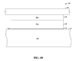
- the resulting copper and tin layers 140 and 150 form (e.g., upon heating) a Cu-Sn alloy, which may also include seed layer 130 as discussed above.
- the thickness of the tin layer 150 varies with different applications, such as to ensure consumption of the tin via combination with the copper in copper layer 140. In some embodiments, the tin layer 150's thickness is around 3 ⁇ m.
- the resulting alloy has a melting point that is desirably low, and in some implementations, around 230°C.
- the Cu-Sn alloy has been heated to its melting point and reacted to form a copper-tin (Cu-Sn) compound 170.
- the resulting compound 170 mechanically and electrically couples the upper package component 160 to the surface 112 of the underlying package component 110.
- the Cu-Sn compound 170 e.g., an intermetallic compound
- the Cu-Sn compound 170 has a melting point that is substantially higher than the melting point of the Cu-Sn alloy.
- the substantially higher melting point is a melting point that is above about 300°C, and in other contexts, the substantially higher melting point is above about 400°C.
- the package components 110 and 160 may include one or more of a variety of components, such as individual bond pad contacts or devices having an array of such contacts.
- various embodiments involve manufacturing a bond-pad sized Cu-Sn compound 170, having dimensions that fit the particular application.
- Other embodiments are directed to the formation of several bond pad connections. These applications are particularly amenable to small-dimension packages, and can be effected without solder prints.
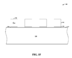
- Figure 1F shows a bond package 100 patterned to suit a particular connectivity pattern of respective package components, before reaction of the Cu-Sn alloy to form a Cu-Sn IMC (e.g., similar to the stage shown in Figure 1D ).
- a plurality of individual bond pad stacks are formed as shown, with stack 180 labeled by way of example.
- One approach to forming the stacks involves patterning the plated copper layer 130 (and, in some instances, the underlying adhesion layer 120 as well), prior to plating a copper layer 142. With this approach, the plated copper 142 is formed on the remaining (patterned) seed layer portions and does not have to be patterned.
- Figure 1G shows the patterned Cu-Sn alloy as reacted to form a Cu-Sn IMC material for coupling an upper package component 162.
- the upper package component 162 may be introduced with a tin layer patterned to match the pattern of plated copper as shown, which reacts to form a Cu-Sn alloy and, further, a Cu-Sn intermetallic compound that joins the package components 110 and 162.
- FIG. 2 is a flow diagram for a method for manufacturing a low-lead or leadless bond package, according to another example embodiment of the present invention.
- an adhesion material is sputtered onto a surface of a package substrate, and a copper (Cu) seed layer is applied to the adhesion material at block 220.
- a copper (Cu) seed layer is applied to the adhesion material at block 220.
- copper is plated onto the seed layer at block 230.
- a tin (Sn) layer is provided on the plated copper layer formed at block 230, to form a copper-tin (Cu-Sn) alloy.
- a secondary package component is positioned for bonding at block 250, such as by bringing one or more bonding pads into contact with the Cu-Sn alloy.
- the secondary package component e.g., a leadframe
- the Cu-Sn alloy is heated to form a Cu-Sn intermetallic compound (IMC) such as Cu 6 Sn 5 .
- IMC Cu-Sn intermetallic compound
- the Cu-Sn IMC exhibits a higher melting point than the Cu-Sn alloy, which facilitates further high-temperature processing.
- a flux is applied (e.g., sprayed) to mitigate the oxidation or other degradation of the materials as the Cu-Sn intermetallic compound is formed, and removed as appropriate after formation of the IMC.
- the positioning of the secondary package component at block 250 may also be carried out in connection with the heating at block 260.
- the Cu-Sn alloy may be heated to melt the alloy, with the secondary package component brought into contact with the alloy before it cools and solidifies.
- the thickness of one or both of the respective copper and tin layers, and sometimes of the adhesion and seed layers as well, are selected together with IMC heating conditions at block 225 to facilitate consumption of the Sn layer provided at block 240 in forming the Cu-Sn IMC at block 260.
- the respective thicknesses can be so chosen along with temperature and time parameters of the heating in the IMC formation at block 260 to ensure the consumption of the Sn layer.
- Such thicknesses and temperatures may include those as discussed herein, such as by heating a 2-4 ⁇ m layer of tin to a temperature of about 230°C for several minutes, an hour or more.
- the respective thicknesses, temperature and time can be set to suit various applications and facilitate the use of these approaches with different types of equipment.
- the thickness selection steps at block 225 may be carried out prior to and/or in connection with any of the steps as shown, such as in connection with one or both of the application of the copper seed layer at block 220 and the sputtering of adhesion material at block 210.
- Dashed lines connecting block 225 to the other blocks represent these exemplary processes, in which thickness and heating conditions are selected for one or more steps as shown.
- the copper seed layer is patterned at block 227, prior to plating the copper layer at block 230.
- the adhesion material is also patterned at block 227. This patterning facilitates the formation of the plated copper at block 230 in a predefined pattern as applied to the copper layer.
- FIG. 3 shows a phase diagram 300 of a copper-tin (Cu-Sn) material as representing materials used in accordance with one or more example embodiments of the present invention.
- a copper-tin compound can be formed from a copper-tin alloy via melting of the alloy and combination of the melted alloy components to form a (solidified) compound having a resulting higher melting temperature.
- the Cu-Sn alloy melts at temperatures approaching and just beyond 200°C.
- this approach is relevant to melting an alloy formed via tin layer 150 and at least a portion of copper layer 140 as shown in Figure 1D , as combined prior to melting to form the IMC 170 in Figure 1E .
- the melting point of the resulting compound is much higher, as the composition of copper increases in the compound.
- the resulting melting temperature is above 400°C.
- FIG. 4 shows a plot 400 of temperature versus copper content for a joining material, in accordance with other example embodiments of the present invention.
- the plot 400 shows a liquid phase above plot 410 at region 420.
- a solid phase is below plot 412 at region 430, and a liquid + Cu-Sn IMC (Cu 6 Sn 5 ) phase is between plots 410 and 412 at region 430.
- the plot 410 represents a line of temperature below which a Cu-Sn alloy is in solid form, and above which melting occurs. Held above the melting temperature for a significant amount of time (and at a sufficiently thin layer of tin), substantially all of the tin reacts with the copper to form a Cu-Sn compound as described. As the Cu-Sn is initially heated, liquid CuSn is formed as shown in liquid region 420. As more of the copper and tin reacts to form a Cu-Sn IMC (Cu 6 Sn 5 ), a combination of liquid + Cu 6 Sn 5 is present and, as the tin is consumed, becomes all Cu 6 Sn 5 (solidified).
Landscapes
- Die Bonding (AREA)
- Lead Frames For Integrated Circuits (AREA)
Abstract
Circuit components (110,160) are joined using a copper-tin (Cu-Sn) alloy. A barrier layer/adhesion promoter (120) is sputtered on a bond connection surface (112) of a package component (110), a seed layer of copper (130) is applied thereon and a copper layer (140) is plated on the seed layer (130). The copper layer (140) is put in contact with a tin layer (150) by positioning a package component (160), having a layer of tin (150) thereon. The copper and tin layers (140,150) are heated to form a Cu-Sn alloy, melt the Cu-Sn alloy and react substantially all of the tin to form a Cu-Sn intermetallic compound (170) from the alloy, physically and electrically coupling components (110,160) together. Component (110) may be a semiconductor or integrated circuit substrate. Component (160) may be a leadframe or a circuit board. The barrier layer/adhesion promoter (120), the Cu seed layer (130) and the plated Cu layer (140) may be patterned. The tin layer (140) may alternatively be formed directly on the plated Cu layer (130).
Description
- Integrated circuits are often fabricated on chips that are connected to a larger package via bond pads and/or other types of electrical connectors, using a connective joining material such as solder. These packages may include multiple circuits and devices, and can be incorporated into larger circuits (e.g., onto a printed circuit board). The packaging process may involve integrating many circuit dies upon a particular package, with connections between each die and the package.
- Many integrated circuit components and related manufacturing processes have been challenging to implement due to issues with materials and processes used in making electrical connections. For example, lead and lead-based materials have been used in solder connectors, but pose environmental challenges on many fronts. In addition, many soldering approaches are susceptible to undesirable characteristics, such as solder voiding, solder splash, flux contamination, misalignment, solder dedicated re-melting temperatures, or peeling, which can be detrimental to device integration and performance.
- These and other matters have presented challenges to connecting integrated circuits, and related device operation.
- Various example embodiments are directed to circuit connectors and approaches to connecting circuits, such as for connecting integrated circuit chips with leadframes using a bond pad.
- In accordance with an example embodiment, an integrated circuit device is manufactured as follows. A metal barrier layer/adhesion promoter is sputtered on a bond connection surface (e.g., a redistribution layer), and a seed layer of copper is applied on the barrier layer/adhesion promoter. Copper is plated on the seed layer to form a plated copper layer. A layer of tin is introduced to the plated copper layer, such as by positioning a circuit component having the layer of tin thereupon, such that the tin layer contacts the plated copper layer. In some implementations, the seed layer and barrier layer/adhesion promoter are patterned to form a bond pad pattern, and copper is galvanically plated on the patterned seed layer to form a patterned metal stack having a pattern that matches the patterned seed layer. The copper and tin is heated to form a Cu-Sn alloy, melt the Cu-Sn alloy, and react substantially all of the tin to form a Cu-Sn intermetallic compound from the alloy. The compound physically and electrically connects the connection surface with another connector (e.g., a copper connector).
- Another example embodiment is directed to a method for joining a semiconductor substrate with a leadframe having tin connectors. A barrier layer/adhesion promoter is sputtered on a surface of the substrate, and a seed layer of copper is sputtered on the barrier layer/adhesion promoter. The seed layer and barrier layer/adhesion promoter are patterned to form a bond pad pattern, and copper is galvanically plated on the patterned seed layer to form a patterned copper layer having a pattern that matches the patterned seed layer. The leadframe (e.g., a copper lead frame that is galvanically tin plated) is positioned to contact the patterned copper layer. The copper and tin are heated to form a Cu-Sn alloy, melt the alloy, and react substantially all of the tin to form a Cu-Sn intermetallic compound that physically and electrically connects the substrate surface with the leadframe.
- In connection with another example embodiment, an integrated circuit package includes an integrated circuit substrate and a leadframe. The substrate includes a bond connection surface, and a sputtered barrier layer/adhesion promoter is located on the connection surface. A seed layer of copper is on the barrier layer/adhesion promoter, and plated copper is on the seed layer. The leadframe has a layer of tin for bonding with the integrated circuit substrate via the plated copper. The tin layer is configured via its thickness to, upon contact with the copper and heating of the copper and tin, form a Cu-Sn alloy that melts, and to form a Cu-Sn intermetallic compound from the alloy via reaction of substantially all of the tin. The compound physically and electrically connecting the connection surface with the leadframe.
- The above discussion/summary is not intended to describe each embodiment or every implementation of the present disclosure. The figures and detailed description that follow also exemplify various embodiments.
- Various example embodiments may be more completely understood in consideration of the following detailed description in connection with the accompanying drawings, in which:
-
FIG. 1 shows a cross-sectional view of a bond package at various stages of manufacture, in accordance with one or more example embodiments of the present invention; -
FIG. 2 is a flow diagram for a method for manufacturing a low-lead or leadless bond package, according to another example embodiment of the present invention; -
FIG. 3 shows a phase diagram of a copper-tin (Cu-Sn) material as used in accordance with one or more example embodiments of the present invention; and -
FIG. 4 shows temperature versus copper content for a joining material, in accordance with other example embodiments of the present invention. - While the invention is amenable to various modifications and alternative forms, specifics thereof have been shown by way of example in the drawings and will be described in detail. It should be understood, however, that the intention is not to limit the invention to the particular embodiments described. On the contrary, the intention is to cover all modifications, equivalents, and alternatives falling within the scope of the invention including aspects defined in the claims.
- The present invention is believed to be applicable to a variety of different types of processes, devices and arrangements for use with various circuits, including integrated circuits coupled into package arrangements using a joining material and related processes. While the present invention is not necessarily so limited, various aspects of the invention may be appreciated through a discussion of examples using this context.
- According to an example embodiment, a copper and tin-based joining material is used to connect circuits in an integrated circuit device. A copper and tin alloy is formed over a surface, heated (melted) and reacted to form a copper-tin (Cu-Sn) intermetallic compound, in which substantially all of the tin is reacted in forming the compound. The Cu-Sn intermetallic compound includes a material such as Cu6Sn5 that both physically and electrically couples the surface and another circuit component. This approach can be carried out, and the resulting structure can be made, in a lead-free manner addressing various challenges including those discussed in the background above.
- The respective thicknesses of the copper and/or tin, as well as other adjacent materials and processing conditions relating to heating are selected to suit various applications and facilitate the reaction of substantially all of the tin. In various applications, reacting substantially all of the tin involves reacting at least 80% of the tin, at least 90% of the tin, at least 95% of the tin or at least 98% of the tin. In addition, various embodiments involving the formation of a Cu-Sn compound involve doing so in a lead-free or substantially lead-free environment.
- In some implementations, the respective thicknesses of the copper and/or tin are set to achieve a selected (low) melting point temperature of the alloy, and a correspondingly higher melting point temperature of the resulting intermetallic compound. The copper and tin alloy is heated to melt/flow the alloy at the desirably low temperature (e.g., around 230 °C), to form the intermetallic compound and join circuit components. As the resulting intermetallic compound is formed, it solidifies and exhibits a relatively higher melting temperature (e.g., at or above about 400 °C).
- According to a more particular example embodiment, a barrier layer/adhesion promoter is used as an interface between the copper and tin alloy and the surface over which the alloy is formed. The barrier layer/adhesion promoter may operate to effect one or both of barrier and adhesion properties and may include, for example, titanium-based material, a nickel-based material an, or a vanadium-based material. The barrier layer/adhesion promoter can be sputtered upon the surface underlying the copper/tin alloy before the formation thereof. In many implementations, the barrier layer/adhesion promoter has barrier properties that mitigate the formation of additional intermetallic compound (in later processing) at a particular temperature.
- The copper and corresponding copper/tin alloy can be formed using a variety of approaches. In one embodiment, a seed layer of copper is applied first and functions as a landing place for subsequently-formed copper (e.g., via galvanic plating), followed by plating of a copper layer on the seed layer to form a plated copper layer. Where a barrier layer/adhesion promoter is used as discussed above, the seed layer of copper is applied to the barrier layer/adhesion promoter, with the combined adhesion-layer material and copper seed layer forming a combined material that facilitates the subsequent plating of the copper layer, from an adhesion and formation perspective. Once the plated copper layer is formed, tin (e.g., a layer) is contacted with the plated copper layer to form a copper-tin (Cu-Sn) alloy.
- The tin (layer) is introduced to and contacts the plated copper in a variety of manners. In one implementation, a tin layer of a selected thickness is formed on an integrated circuit package component, such as a leadframe, to be joined to a chip on which the plated copper is formed. The integrated circuit package component is then positioned to contact the tin layer with the plated copper. In another implementation, a tin layer is formed directly on the plated copper layer. In these (or other) implementations, the thickness of the tin layer can be set thin enough such that all of the tin is consumed in a subsequent reaction to form an intermetallic compound, as discussed further below.
- Upon heating, the copper and tin in the Cu-Sn alloy melt and the copper and tin in the melted alloy react to form a copper-tin (Cu-Sn) intermetallic compound. During the reaction, all or substantially all of the tin reacts. This compound physically (e.g., mechanically) and electrically couples the underlying surface with the resulting (overlying) circuit. This approach is applicable to joining a bond package arrangement in which a package component such as a silicon chip is joined to another package component such as a leadframe.
- In some embodiments, upper and lower surfaces of an integrated circuit chip are coated with a barrier layer/adhesion promoter and copper seed layer, and subsequently plated with copper as described herein. Additional package components are subsequently connected to each side of the chip, using a tin layer as discussed to form a copper-tin alloy and, therefrom, a copper-tin intermetallic compound via consumption of the tin.
- In connection with various example embodiments, it has been discovered that the respective thicknesses of layers including one or more of respective copper and tin materials, adhesion material and seed material can be set together with the temperature and time at which the Cu-Sn alloy is heated to effect the reaction of substantially all of the Sn to form the Cu-Sn intermetallic compound. The respective layers are formed to the set thicknesses, and the materials are subjected to heating at the set temperature for the selected time, to form the Cu-Sn intermetallic compound.
- In some embodiments, respective layer thicknesses as discussed above include a 0.2µm layer of Titanium adhesion material, a 0.2µm seed layer of copper, a 5µm plated copper layer and a 3µm layer of tin. The thickness of the tin layer is varied, in connection with different embodiments, to ensure the consumption of the tin in forming a Cu-Sn compound with the underlying copper.
- The package components that the Cu-Sn alloy is used to connect may vary depending upon the application. For example, the alloy (and subsequent compound) can be formed on an underlying surface of a circuit board or other package component, with another package component such as a leadframe added above and coupled with the underlying surface via heating and reaction to form the Cu-Sn compound. For instance, bond pads of respective circuits on different package components can be connected to one another using this approach. In addition, the alloy (and subsequent compound) can also be formed upon the underside of a device such as a circuit or package component, to be coupled to an underlying circuit board (or other package component).
- As consistent with the examples discussed herein, various embodiments are directed to integrated circuits, circuit packages, circuit boards and related devices employing a copper-tin based joining material as described. Other embodiments are directed to methods for manufacturing such circuits, packages, boards and devices using the copper-tin based joining material.
- Still other embodiments are directed to devices at an intermediate stage of manufacture. For example, one such embodiment is directed to an intermediate device having a copper/tin alloy material, together with one or more related materials and material layers as described (e.g., adhesion and/or seed layers). The intermediate device and the respective layers are configured for subsequent heating, at an appropriate stage of further manufacture, when the device is joined to another package component. Other examples involve devices at other stages of manufacture, such as a device amenable to the addition of tin to a plated copper layer that has been prepared for further processing. For instance, such embodiments may involve one or both components of a two-component package (e.g., chip and leadframe) that is yet to be joined, with one component having a plated copper layer and the other component having a tin layer, as discussed. Various embodiments are also directed to methods for manufacturing such devices.
- Turning now to the Figures,
Figure 1 shows abond package 100 at various stages of manufacture, in accordance with one or more example embodiments of the present invention. Each of the various stages represent different embodiments, such as may pertain to a device at different stages of manufacture and the corresponding manufacturing steps to get to the respective stages. In addition, the respective stages may be implemented together as part of a manufacturing process in accordance with a more particular embodiment. Moreover, other embodiments involve later stages of manufacture, in which a package is provided at an intermediate stage of manufacture and further manufacturing steps are carried out. Still other embodiments are directed to the implementation of intermediate stages of manufacture, where a package is received at an earlier stage of processing and provided at a later stage of processing but prior to completion. - Beginning with
Figure 1A , apackage component 110 is/has been treated at itssurface 112 with a barrier layer/adhesion promoter 120, which may be applied via sputtering (represented by arrows 122). The barrier layer/adhesion promoter layer 120 includes one or more of a variety of materials that facilitate the adhesion of the surface and act as a diffusion barrier to surface 112 with an overlying copper-tin layer component (e.g., with a copper layer formed upon the adhesion promoter layer). - In
Figure 1B , acopper seed layer 130 is shown formed on a barrier layer/adhesion promoter 120, which may also be applied via sputtering as represented witharrows 132. Theseed layer 130 may be formed using a liquid-liquid-solid formation approach relating to different liquid and solid phases of the copper in the seed layer. The respective thicknesses of the barrier layer /adhesion promoter 120 and theseed layer 132 are selected to suit the particular application. In some implementations, the thicknesses are about equal, and in a more particular implementation, the thicknesses are about 0.2 µm. In some embodiments, thecopper seed layer 130 is patterned, as shown inFigure 1F and described further below. - In
Figure 1C , a copper (Cu)layer 140 has been plated on underlying adhesion and copper seed layers 120 and 130. The adhesion layer facilitates adhesion of the copper seed layer, which may effectively become part of the resulting copper layer 140 (as would include the seed layer 130). In this context, thecopper layer 140 may be adhered directly to thesurface 112 of theunderlying package component 110. The thickness of thecopper layer 140 varies with implementations, and in some embodiments, is around 5 µm. - In
Figure 1D , a tin (Sn)layer 150 has been formed (e.g., plated) on anupper package component 160, such as a leadframe, which is positioned to contact the tin layer with thecopper layer 140. As with thepackage component 110, theupper package component 160 is represented in cross-section with the further understanding that the height and width of the package may vary (relatively) in different applications. The resulting copper andtin layers seed layer 130 as discussed above. The thickness of thetin layer 150 varies with different applications, such as to ensure consumption of the tin via combination with the copper incopper layer 140. In some embodiments, thetin layer 150's thickness is around 3 µm. The resulting alloy has a melting point that is desirably low, and in some implementations, around 230°C. - In
Figure 1E , the Cu-Sn alloy has been heated to its melting point and reacted to form a copper-tin (Cu-Sn)compound 170. The resultingcompound 170 mechanically and electrically couples theupper package component 160 to thesurface 112 of theunderlying package component 110. The Cu-Sn compound 170 (e.g., an intermetallic compound) has a desirably high melting point. In some embodiments, the Cu-Sn compound 170 has a melting point that is substantially higher than the melting point of the Cu-Sn alloy. In some contexts, the substantially higher melting point is a melting point that is above about 300°C, and in other contexts, the substantially higher melting point is above about 400°C. - The
package components Sn compound 170, having dimensions that fit the particular application. Other embodiments are directed to the formation of several bond pad connections. These applications are particularly amenable to small-dimension packages, and can be effected without solder prints. - As an example of bond pad arrangements,
Figure 1F shows abond package 100 patterned to suit a particular connectivity pattern of respective package components, before reaction of the Cu-Sn alloy to form a Cu-Sn IMC (e.g., similar to the stage shown inFigure 1D ). A plurality of individual bond pad stacks are formed as shown, withstack 180 labeled by way of example. One approach to forming the stacks involves patterning the plated copper layer 130 (and, in some instances, theunderlying adhesion layer 120 as well), prior to plating acopper layer 142. With this approach, the platedcopper 142 is formed on the remaining (patterned) seed layer portions and does not have to be patterned. -
Figure 1G shows the patterned Cu-Sn alloy as reacted to form a Cu-Sn IMC material for coupling anupper package component 162. As consistent with the embodiment shown inFigure 1D , theupper package component 162 may be introduced with a tin layer patterned to match the pattern of plated copper as shown, which reacts to form a Cu-Sn alloy and, further, a Cu-Sn intermetallic compound that joins thepackage components -
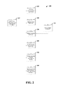
FIG. 2 is a flow diagram for a method for manufacturing a low-lead or leadless bond package, according to another example embodiment of the present invention. Atblock 210, an adhesion material is sputtered onto a surface of a package substrate, and a copper (Cu) seed layer is applied to the adhesion material atblock 220. Using the copper seed layer, copper is plated onto the seed layer atblock 230. - At
block 240, a tin (Sn) layer is provided on the plated copper layer formed atblock 230, to form a copper-tin (Cu-Sn) alloy. A secondary package component is positioned for bonding atblock 250, such as by bringing one or more bonding pads into contact with the Cu-Sn alloy. In many applications, the secondary package component (e.g., a leadframe) has the layer of Sn, which is contacted to the plated copper layer formed atblock 230. Atblock 260, the Cu-Sn alloy is heated to form a Cu-Sn intermetallic compound (IMC) such as Cu6Sn5. After solidification, the Cu-Sn IMC exhibits a higher melting point than the Cu-Sn alloy, which facilitates further high-temperature processing. In some implementations, a flux is applied (e.g., sprayed) to mitigate the oxidation or other degradation of the materials as the Cu-Sn intermetallic compound is formed, and removed as appropriate after formation of the IMC. - The positioning of the secondary package component at
block 250 may also be carried out in connection with the heating atblock 260. For example, the Cu-Sn alloy may be heated to melt the alloy, with the secondary package component brought into contact with the alloy before it cools and solidifies. - In some embodiments, the thickness of one or both of the respective copper and tin layers, and sometimes of the adhesion and seed layers as well, are selected together with IMC heating conditions at
block 225 to facilitate consumption of the Sn layer provided atblock 240 in forming the Cu-Sn IMC atblock 260. For instance, as discussed in connection with the above discovery-type embodiments, the respective thicknesses can be so chosen along with temperature and time parameters of the heating in the IMC formation atblock 260 to ensure the consumption of the Sn layer. Such thicknesses and temperatures may include those as discussed herein, such as by heating a 2-4µm layer of tin to a temperature of about 230°C for several minutes, an hour or more. As would be understood, the respective thicknesses, temperature and time can be set to suit various applications and facilitate the use of these approaches with different types of equipment. As appropriate, the thickness selection steps atblock 225 may be carried out prior to and/or in connection with any of the steps as shown, such as in connection with one or both of the application of the copper seed layer atblock 220 and the sputtering of adhesion material atblock 210. Dashedlines connecting block 225 to the other blocks represent these exemplary processes, in which thickness and heating conditions are selected for one or more steps as shown. - In certain embodiments, the copper seed layer is patterned at
block 227, prior to plating the copper layer atblock 230. In some implementations, the adhesion material is also patterned atblock 227. This patterning facilitates the formation of the plated copper atblock 230 in a predefined pattern as applied to the copper layer. -
FIG. 3 shows a phase diagram 300 of a copper-tin (Cu-Sn) material as representing materials used in accordance with one or more example embodiments of the present invention. Based upon this phase diagram, a copper-tin compound can be formed from a copper-tin alloy via melting of the alloy and combination of the melted alloy components to form a (solidified) compound having a resulting higher melting temperature. As can be seen near the right-most portion of the phase diagram, the Cu-Sn alloy melts at temperatures approaching and just beyond 200°C. Referring toFigure 1 , this approach is relevant to melting an alloy formed viatin layer 150 and at least a portion ofcopper layer 140 as shown inFigure 1D , as combined prior to melting to form theIMC 170 inFigure 1E . When the tin is reacted with copper, the melting point of the resulting compound is much higher, as the composition of copper increases in the compound. For Cu6Sn5 at a copper percentage of about 55%, the resulting melting temperature is above 400°C. -
FIG. 4 shows aplot 400 of temperature versus copper content for a joining material, in accordance with other example embodiments of the present invention. As consistent with the above discussion inFigure 3 , theplot 400 shows a liquid phase aboveplot 410 atregion 420. A solid phase is belowplot 412 atregion 430, and a liquid + Cu-Sn IMC (Cu6Sn5) phase is betweenplots region 430. - The
plot 410 represents a line of temperature below which a Cu-Sn alloy is in solid form, and above which melting occurs. Held above the melting temperature for a significant amount of time (and at a sufficiently thin layer of tin), substantially all of the tin reacts with the copper to form a Cu-Sn compound as described. As the Cu-Sn is initially heated, liquid CuSn is formed as shown inliquid region 420. As more of the copper and tin reacts to form a Cu-Sn IMC (Cu6Sn5), a combination of liquid + Cu6Sn5 is present and, as the tin is consumed, becomes all Cu6Sn5 (solidified). - Based upon the above discussion and illustrations, those skilled in the art will readily recognize that various modifications and changes may be made to the present invention without strictly following the exemplary embodiments and applications illustrated and described herein. For example, the content of the copper/tin (Cu-Sn) materials as shown may be varied depending upon the application, as may be the relative thickness and placement as shown in and/or described in connection with the figures, or otherwise. In addition, the phase of the resulting intermetallic compound of Cu-Sn material may vary, depending upon the application. Such modifications do not depart from the true spirit and scope of the present invention, including that set forth in the following claims.
Claims (20)
- A method for manufacturing an integrated circuit device, the method comprising:sputtering a barrier layer-adhesion promoter on a bond connection surface;applying a seed layer of Cu on the barrier layer-adhesion promoter;plating Cu on the seed layer to form a plated Cu layer;introducing a layer of Sn to the plated Cu layer;heating the Cu and Sn to form a Cu-Sn alloy, melt the Cu-Sn alloy, and react substantially all of the Sn to form a Cu-Sn intermetallic compound from the alloy, the Cu-Sn intermetallic compound physically and electrically connecting the connection surface with another connector via.
- The method of claim 1,
further including selecting the thickness of the Sn layer and both the temperature and time at which to heat the device to effect the reaction of substantially all of the Sn to form the Cu-Sn intermetallic compound,
providing a layer of Sn includes forming the layer to the selected thicknesses, wherein heating includes heating the Cu-Sn alloy to the selected temperature for the selected time. - The method of claim 1,
further including patterning the seed layer of Cu, prior to plating Cu, and
herein plating Cu on the seed layer introducing a layer of Sn to the plated Cu layer includes plating Cu on the patterned seed layer to form a patterned Cu layer matching the pattern of the pattered seed layer. - The method of claim 1, wherein introducing a layer of Sn to the plated Cu layer includes placing a leadframe with a layer of Sn thereupon onto the plated Cu.
- The method of claim 1, wherein heating to react substantially all of the Sn to form a Cu-Sn intermetallic compound includes forming a Cu-Sn intermetallic compound that is substantially free of lead.
- The method of claim 1, wherein heating to react substantially all of the Sn to form a Cu-Sn intermetallic compound includes forming Cu6Sn5.
- The method of claim 1, wherein heating to react substantially all of the Sn to form a Cu-Sn intermetallic compound includes forming a Cu-Sn intermetallic compound having a melting point that is substantially higher than the melting point of the Cu-Sn alloy.
- The method of claim 1, wherein sputtering a barrier layer-adhesion promoter on a connection surface includes sputtering at least one of titanium, aluminum, nickel and vanadium.
- The method of claim 1, wherein sputtering an adhesion promoter on a connection surface includes sputtering a 0.2 µm layer of an adhesion promoter.
- The method of claim 1, wherein applying a seed layer of Cu on the adhesion promoter includes applying a 0.2 µm layer of Cu.
- The method of claim 1, wherein plating Cu on the seed layer to form a plated Cu layer includes plating a 5 µm layer of Cu.
- The method of claim 1, further including forming the layer of Sn to a thickness of about 3 µm.
- The method of claim 1, wherein
sputtering a barrier layer-adhesion promoter on a connection surface includes sputtering a 0.2 µm layer of the adhesion promoter,
applying a seed layer of Cu on the barrier layer-adhesion promoter includes applying a 0.2 µm layer of Cu,
plating Cu on the seed layer to form a plated Cu layer includes plating a 5 µm layer of Cu, and
forming a layer of Sn includes forming a 3 µm layer of Sn on the plated Cu layer. - The method of claim 1, wherein
forming a layer of Sn on the plated Cu layer to form a Cu-Sn alloy includes forming a Cu-Sn alloy having a melting point that is less than about 230°C, and
reacting substantially all of the Sn to form a Cu-Sn intermetallic compound includes forming a Cu-Sn intermetallic compound having a re-melting temperature of at least about 400°C. - The method of claim 1, further including applying a flux material to the Cu-Sn alloy, before heating the Cu-Sn alloy, to mitigate oxidation of the Cu-Sn alloy.
- The method of claim 1, further including patterning the Cu-Sn alloy, prior to heating of the alloy and forming the Cu-Sn intermetallic compound.
- A method for joining a semiconductor substrate with a leadframe having tin connectors, the method comprising:sputtering a barrier layer-adhesion promoter on a surface of the substrate;sputtering a seed layer of Cu on the barrier layer-adhesion promoter;patterning the seed layer and adhesion promoter to form a bond pad pattern;galvanically plating Cu on the patterned seed layer to form a patterned Cu layer having a pattern that matches the patterned seed layer;positioning the leadframe to contact the tin connectors with the patterned Cu layer;heating the Cu and Sn forming a Cu-Sn alloy, melting the alloy, and reacting substantially all of the Sn to form a Cu-Sn intermetallic compound that physically and electrically connects the substrate surface with the leadframe.
- An integrated circuit package comprising:an integrated circuit substrate havinga sputtered adhesion promoter on a bond connection surface of the substrate,a seed layer of Cu on the adhesion promoter, andplated Cu on the seed layer; anda leadframe having a layer of Sn for bonding with the integrated circuit substrate via the plated Cu, the layer of Sn being configured via its thickness toupon contact with the Cu and heating of the Cu and Sn, form a Cu-Sn alloy that melts, andform a Cu-Sn intermetallic compound from the alloy via reaction of substantially all of the Sn, the compound physically and electrically connecting the connection surface with the leadframe.
- The integrated circuit package of claim 18, wherein
the seed layer of Cu is a patterned layer,
the plated Cu has a pattern that matches the pattern of the seed layer, and
the layer of Sn on the leadframe is a patterned layer having a pattern that matches the pattern of the plated Cu. - The integrated circuit package of claim 18, wherein the layer of Sn is configured via its thickness to form the Cu-Sn intermetallic compound via consumption of substantially all of the Sn at a selected temperature that is at least about the melting point of the Cu-Sn alloy, the Cu-Sn intermetallic compound having a melting point that is substantially higher than the melting point of the Cu-Sn alloy.
Priority Applications (3)
| Application Number | Priority Date | Filing Date | Title |
|---|---|---|---|
| EP10166436A EP2398046A1 (en) | 2010-06-18 | 2010-06-18 | Integrated circuit package with a copper-tin joining layer and manufacturing method thereof |
| CN2011101622003A CN102290357A (en) | 2010-06-18 | 2011-06-16 | Bonding packaging and method thereof |
| US13/163,443 US20120162958A1 (en) | 2010-06-18 | 2011-06-17 | Bond package and approach therefor |
Applications Claiming Priority (1)
| Application Number | Priority Date | Filing Date | Title |
|---|---|---|---|
| EP10166436A EP2398046A1 (en) | 2010-06-18 | 2010-06-18 | Integrated circuit package with a copper-tin joining layer and manufacturing method thereof |
Publications (1)
| Publication Number | Publication Date |
|---|---|
| EP2398046A1 true EP2398046A1 (en) | 2011-12-21 |
Family
ID=42561223
Family Applications (1)
| Application Number | Title | Priority Date | Filing Date |
|---|---|---|---|
| EP10166436A Withdrawn EP2398046A1 (en) | 2010-06-18 | 2010-06-18 | Integrated circuit package with a copper-tin joining layer and manufacturing method thereof |
Country Status (3)
| Country | Link |
|---|---|
| US (1) | US20120162958A1 (en) |
| EP (1) | EP2398046A1 (en) |
| CN (1) | CN102290357A (en) |
Cited By (1)
| Publication number | Priority date | Publication date | Assignee | Title |
|---|---|---|---|---|
| EP2858107A3 (en) * | 2013-09-09 | 2015-10-21 | Kabushiki Kaisha Toshiba | Semiconductor device with a bonding layer with a region comprising Ti and a region comprising Sn but with substantially no region comprising both Ti and Sn and method for manufacturing the same |
Families Citing this family (12)
| Publication number | Priority date | Publication date | Assignee | Title |
|---|---|---|---|---|
| JP6225453B2 (en) * | 2012-05-24 | 2017-11-08 | 日亜化学工業株式会社 | Semiconductor device |
| CN103264202B (en) * | 2012-12-27 | 2016-12-28 | 中国电子科技集团公司第四十一研究所 | A kind of brazing layer pre-deposited method |
| CN103658899B (en) * | 2013-12-04 | 2016-04-13 | 哈尔滨工业大学深圳研究生院 | The preparations and applicatio method of the micro-interconnection welding spot structure of a kind of single-orientated Cu6Sn5 intermetallic compound |
| JP2015165527A (en) * | 2014-02-28 | 2015-09-17 | 株式会社東芝 | Semiconductor device and manufacturing method of the same |
| JP6288284B2 (en) * | 2014-09-10 | 2018-03-07 | 株式会社村田製作所 | Method for producing intermetallic compound |
| US9564409B2 (en) * | 2015-01-27 | 2017-02-07 | Semiconductor Components Industries, Llc | Methods of forming semiconductor packages with an intermetallic layer comprising tin and at least one of silver, copper or nickel |
| CN105047604B (en) * | 2015-07-03 | 2018-05-11 | 哈尔滨工业大学深圳研究生院 | Cu under a kind of three-dimension packaging interconnection solder joint6Sn5The synthetic method of phase monocrystal diffusion impervious layer |
| CN105171168B (en) * | 2015-07-13 | 2018-03-30 | 哈尔滨工业大学深圳研究生院 | A kind of High-temperature Packaging Cu6Sn5The orientation interconnecting method of base monocrystalline Lead-Free Solder Joint |
| US10115716B2 (en) * | 2015-07-18 | 2018-10-30 | Semiconductor Components Industries, Llc | Die bonding to a board |
| US10796956B2 (en) * | 2018-06-29 | 2020-10-06 | Texas Instruments Incorporated | Contact fabrication to mitigate undercut |
| CN111739854B (en) * | 2020-07-06 | 2022-03-29 | 绍兴同芯成集成电路有限公司 | Thick copper film of two-sided electroplating of windowing |
| CN114245569B (en) * | 2022-01-11 | 2023-06-23 | 刘良江 | LCP-based high-frequency ultrahigh-frequency flexible circuit board manufacturing method |
Citations (5)
| Publication number | Priority date | Publication date | Assignee | Title |
|---|---|---|---|---|
| US20050103636A1 (en) * | 2003-11-18 | 2005-05-19 | International Business Machines Corporation | Method for selective electroplating of semiconductor device i/o pads using a titanium-tungsten seed layer |
| US20070205253A1 (en) * | 2006-03-06 | 2007-09-06 | Infineon Technologies Ag | Method for diffusion soldering |
| US20080230905A1 (en) * | 2007-03-19 | 2008-09-25 | Karsten Guth | Power Semiconductor Module, Method for Producing a Power Semiconductor Module, and Semiconductor Chip |
| WO2008157822A1 (en) * | 2007-06-20 | 2008-12-24 | Flipchip International, Llc | Under bump metallization structure having a seed layer for electroless nickel deposition |
| WO2009085609A2 (en) * | 2007-12-28 | 2009-07-09 | Freescale Semiconductor Inc. | 3-d semiconductor die structure with containing feature and method |
Family Cites Families (2)
| Publication number | Priority date | Publication date | Assignee | Title |
|---|---|---|---|---|
| JP4035733B2 (en) * | 2005-01-19 | 2008-01-23 | セイコーエプソン株式会社 | Manufacturing method of semiconductor device and processing method of electrical connection part |
| JP5501586B2 (en) * | 2008-08-22 | 2014-05-21 | ルネサスエレクトロニクス株式会社 | Manufacturing method of semiconductor device |
-
2010
- 2010-06-18 EP EP10166436A patent/EP2398046A1/en not_active Withdrawn
-
2011
- 2011-06-16 CN CN2011101622003A patent/CN102290357A/en active Pending
- 2011-06-17 US US13/163,443 patent/US20120162958A1/en not_active Abandoned
Patent Citations (5)
| Publication number | Priority date | Publication date | Assignee | Title |
|---|---|---|---|---|
| US20050103636A1 (en) * | 2003-11-18 | 2005-05-19 | International Business Machines Corporation | Method for selective electroplating of semiconductor device i/o pads using a titanium-tungsten seed layer |
| US20070205253A1 (en) * | 2006-03-06 | 2007-09-06 | Infineon Technologies Ag | Method for diffusion soldering |
| US20080230905A1 (en) * | 2007-03-19 | 2008-09-25 | Karsten Guth | Power Semiconductor Module, Method for Producing a Power Semiconductor Module, and Semiconductor Chip |
| WO2008157822A1 (en) * | 2007-06-20 | 2008-12-24 | Flipchip International, Llc | Under bump metallization structure having a seed layer for electroless nickel deposition |
| WO2009085609A2 (en) * | 2007-12-28 | 2009-07-09 | Freescale Semiconductor Inc. | 3-d semiconductor die structure with containing feature and method |
Non-Patent Citations (5)
| Title |
|---|
| ALAN HUFFMAN ET AL: "Effects of Assembly Process Parameters on the Structure and Thermal Stability of Sn-Capped Cu Bump Bonds", ELECTRONIC COMPONENTS AND TECHNOLOGY CONFERENCE, 2007. ECTC '07. PROCEEDINGS. 57TH, IEEE, PI, 1 May 2007 (2007-05-01), pages 1589 - 1596, XP031180708, ISBN: 978-1-4244-0984-6 * |
| BYUNGHOON LEE ET AL: "A Study on the Bonding Process of Cu Bump/Sn/Cu Bump Bonding Structure for 3D Packaging Applications", JOURNAL OF THE ELECTROCHEMICAL SOCIETY, vol. 157, no. 4, 18 February 2010 (2010-02-18), pages H420 - H424, XP055001788, ISSN: 0013-4651, DOI: 10.1149/1.3301931 * |
| SCHAPER L ET AL: "Integrated System Development for 3-D VLSI", VLSI PACKAGING WORKSHOP OF JAPAN, 2008. VPWJ 2008. IEEE 9TH, IEEE, PISCATAWAY, NJ, USA, 1 December 2008 (2008-12-01), pages 145 - 148, XP031412758, ISBN: 978-1-4244-3498-5 * |
| YIBO RONG ET AL: "Low Temperature Cu-Sn Bonding by Isothermal Solidification Technology", ELECTRONIC PACKAGING TECHNOLOGY & HIGH DENSITY PACKAGING, 2009. ICEPT-HDP '09. INTERNATIONAL CONFERENCE ON, IEEE, PISCATAWAY, NJ, USA, 10 August 2009 (2009-08-10), pages 96 - 98, XP031533513, ISBN: 978-1-4244-4658-2 * |
| ZHIHONG HUANG ET AL: "Electromigration of Cu-Sn-Cu Micropads in 3D Interconnect", 58TH ELECTRONIC COMPONENTS AND TECHNOLOGY CONFERENCE - 27-30 MAY 2008, IEEE, PISCATAWAY, NJ, USA, 27 May 2008 (2008-05-27), pages 12 - 17, XP031276163, ISBN: 978-1-4244-2230-2 * |
Cited By (1)
| Publication number | Priority date | Publication date | Assignee | Title |
|---|---|---|---|---|
| EP2858107A3 (en) * | 2013-09-09 | 2015-10-21 | Kabushiki Kaisha Toshiba | Semiconductor device with a bonding layer with a region comprising Ti and a region comprising Sn but with substantially no region comprising both Ti and Sn and method for manufacturing the same |
Also Published As
| Publication number | Publication date |
|---|---|
| CN102290357A (en) | 2011-12-21 |
| US20120162958A1 (en) | 2012-06-28 |
Similar Documents
| Publication | Publication Date | Title |
|---|---|---|
| EP2398046A1 (en) | Integrated circuit package with a copper-tin joining layer and manufacturing method thereof | |
| TWI356460B (en) | Semiconductor device including electrically conduc | |
| US8643165B2 (en) | Semiconductor device having agglomerate terminals | |
| KR100454381B1 (en) | Semiconductor device and manufacturing method thereof | |
| US9331043B1 (en) | Localized sealing of interconnect structures in small gaps | |
| US20020192935A1 (en) | Semiconductor die including conductive columns | |
| US9754909B2 (en) | Copper structures with intermetallic coating for integrated circuit chips | |
| KR20100128275A (en) | Thermal Machine Flip Chip Die Bonding | |
| US9847310B2 (en) | Flip chip bonding alloys | |
| EP3951842A3 (en) | Pre-plating of solder layer on solderable elements for diffusion soldering, corresponding circuit carrier and corresponding method of soldering electronic components | |
| US20100167466A1 (en) | Semiconductor package substrate with metal bumps | |
| JP2001060760A (en) | Circuit electrode and method for forming the same | |
| TW201225209A (en) | Semiconductor device and method of confining conductive bump material with solder mask patch | |
| JP6593119B2 (en) | Electrode structure, bonding method, and semiconductor device | |
| US9601374B2 (en) | Semiconductor die assembly | |
| US7701061B2 (en) | Semiconductor device with solder balls having high reliability | |
| JP3284034B2 (en) | Semiconductor device and manufacturing method thereof | |
| JP2001094004A (en) | Semiconductor device, external connection terminal structure, and method of manufacturing semiconductor device | |
| US8101462B2 (en) | Method for manufacturing semiconductor device, and semiconductor device | |
| JP2006120803A (en) | Semiconductor device and manufacturing method of semiconductor device | |
| JP3204142B2 (en) | Semiconductor device manufacturing method and lead frame | |
| KR100860445B1 (en) | Semiconductor device and manufacturing method of bond pad | |
| JPH0210840A (en) | Multilayer metal structure for electronic component | |
| JPH0878419A (en) | Bump and method of manufacturing semiconductor device using the same | |
| HK1061741A1 (en) | Fluxless flip chip interconnection |
Legal Events
| Date | Code | Title | Description |
|---|---|---|---|
| AK | Designated contracting states |
Kind code of ref document: A1 Designated state(s): AL AT BE BG CH CY CZ DE DK EE ES FI FR GB GR HR HU IE IS IT LI LT LU LV MC MK MT NL NO PL PT RO SE SI SK SM TR |
|
| AX | Request for extension of the european patent |
Extension state: BA ME RS |
|
| PUAI | Public reference made under article 153(3) epc to a published international application that has entered the european phase |
Free format text: ORIGINAL CODE: 0009012 |
|
| STAA | Information on the status of an ep patent application or granted ep patent |
Free format text: STATUS: THE APPLICATION IS DEEMED TO BE WITHDRAWN |
|
| 18D | Application deemed to be withdrawn |
Effective date: 20120622 |