EP2396861B1 - Hybrid vertical-cavity laser - Google Patents
Hybrid vertical-cavity laser Download PDFInfo
- Publication number
- EP2396861B1 EP2396861B1 EP10701195.9A EP10701195A EP2396861B1 EP 2396861 B1 EP2396861 B1 EP 2396861B1 EP 10701195 A EP10701195 A EP 10701195A EP 2396861 B1 EP2396861 B1 EP 2396861B1
- Authority
- EP
- European Patent Office
- Prior art keywords
- grating
- silicon layer
- grating region
- refractive index
- region
- Prior art date
- Legal status (The legal status is an assumption and is not a legal conclusion. Google has not performed a legal analysis and makes no representation as to the accuracy of the status listed.)
- Not-in-force
Links
Images


Classifications
-
- H—ELECTRICITY
- H01—ELECTRIC ELEMENTS
- H01S—DEVICES USING THE PROCESS OF LIGHT AMPLIFICATION BY STIMULATED EMISSION OF RADIATION [LASER] TO AMPLIFY OR GENERATE LIGHT; DEVICES USING STIMULATED EMISSION OF ELECTROMAGNETIC RADIATION IN WAVE RANGES OTHER THAN OPTICAL
- H01S5/00—Semiconductor lasers
- H01S5/10—Construction or shape of the optical resonator, e.g. extended or external cavity, coupled cavities, bent-guide, varying width, thickness or composition of the active region
- H01S5/18—Surface-emitting [SE] lasers, e.g. having both horizontal and vertical cavities
- H01S5/183—Surface-emitting [SE] lasers, e.g. having both horizontal and vertical cavities having only vertical cavities, e.g. vertical cavity surface-emitting lasers [VCSEL]
- H01S5/18361—Structure of the reflectors, e.g. hybrid mirrors
-
- H—ELECTRICITY
- H01—ELECTRIC ELEMENTS
- H01S—DEVICES USING THE PROCESS OF LIGHT AMPLIFICATION BY STIMULATED EMISSION OF RADIATION [LASER] TO AMPLIFY OR GENERATE LIGHT; DEVICES USING STIMULATED EMISSION OF ELECTROMAGNETIC RADIATION IN WAVE RANGES OTHER THAN OPTICAL
- H01S5/00—Semiconductor lasers
- H01S5/10—Construction or shape of the optical resonator, e.g. extended or external cavity, coupled cavities, bent-guide, varying width, thickness or composition of the active region
- H01S5/11—Comprising a photonic bandgap structure
-
- H—ELECTRICITY
- H01—ELECTRIC ELEMENTS
- H01S—DEVICES USING THE PROCESS OF LIGHT AMPLIFICATION BY STIMULATED EMISSION OF RADIATION [LASER] TO AMPLIFY OR GENERATE LIGHT; DEVICES USING STIMULATED EMISSION OF ELECTROMAGNETIC RADIATION IN WAVE RANGES OTHER THAN OPTICAL
- H01S5/00—Semiconductor lasers
- H01S5/10—Construction or shape of the optical resonator, e.g. extended or external cavity, coupled cavities, bent-guide, varying width, thickness or composition of the active region
- H01S5/18—Surface-emitting [SE] lasers, e.g. having both horizontal and vertical cavities
- H01S5/183—Surface-emitting [SE] lasers, e.g. having both horizontal and vertical cavities having only vertical cavities, e.g. vertical cavity surface-emitting lasers [VCSEL]
- H01S5/18308—Surface-emitting [SE] lasers, e.g. having both horizontal and vertical cavities having only vertical cavities, e.g. vertical cavity surface-emitting lasers [VCSEL] having a special structure for lateral current or light confinement
- H01S5/18311—Surface-emitting [SE] lasers, e.g. having both horizontal and vertical cavities having only vertical cavities, e.g. vertical cavity surface-emitting lasers [VCSEL] having a special structure for lateral current or light confinement using selective oxidation
-
- H—ELECTRICITY
- H01—ELECTRIC ELEMENTS
- H01S—DEVICES USING THE PROCESS OF LIGHT AMPLIFICATION BY STIMULATED EMISSION OF RADIATION [LASER] TO AMPLIFY OR GENERATE LIGHT; DEVICES USING STIMULATED EMISSION OF ELECTROMAGNETIC RADIATION IN WAVE RANGES OTHER THAN OPTICAL
- H01S5/00—Semiconductor lasers
- H01S5/10—Construction or shape of the optical resonator, e.g. extended or external cavity, coupled cavities, bent-guide, varying width, thickness or composition of the active region
- H01S5/18—Surface-emitting [SE] lasers, e.g. having both horizontal and vertical cavities
- H01S5/183—Surface-emitting [SE] lasers, e.g. having both horizontal and vertical cavities having only vertical cavities, e.g. vertical cavity surface-emitting lasers [VCSEL]
- H01S5/18361—Structure of the reflectors, e.g. hybrid mirrors
- H01S5/1838—Reflector bonded by wafer fusion or by an intermediate compound
-
- H—ELECTRICITY
- H01—ELECTRIC ELEMENTS
- H01S—DEVICES USING THE PROCESS OF LIGHT AMPLIFICATION BY STIMULATED EMISSION OF RADIATION [LASER] TO AMPLIFY OR GENERATE LIGHT; DEVICES USING STIMULATED EMISSION OF ELECTROMAGNETIC RADIATION IN WAVE RANGES OTHER THAN OPTICAL
- H01S5/00—Semiconductor lasers
- H01S5/10—Construction or shape of the optical resonator, e.g. extended or external cavity, coupled cavities, bent-guide, varying width, thickness or composition of the active region
- H01S5/18—Surface-emitting [SE] lasers, e.g. having both horizontal and vertical cavities
- H01S5/183—Surface-emitting [SE] lasers, e.g. having both horizontal and vertical cavities having only vertical cavities, e.g. vertical cavity surface-emitting lasers [VCSEL]
- H01S5/18386—Details of the emission surface for influencing the near- or far-field, e.g. a grating on the surface
-
- H—ELECTRICITY
- H01—ELECTRIC ELEMENTS
- H01S—DEVICES USING THE PROCESS OF LIGHT AMPLIFICATION BY STIMULATED EMISSION OF RADIATION [LASER] TO AMPLIFY OR GENERATE LIGHT; DEVICES USING STIMULATED EMISSION OF ELECTROMAGNETIC RADIATION IN WAVE RANGES OTHER THAN OPTICAL
- H01S5/00—Semiconductor lasers
- H01S5/02—Structural details or components not essential to laser action
- H01S5/0206—Substrates, e.g. growth, shape, material, removal or bonding
- H01S5/021—Silicon based substrates
-
- H—ELECTRICITY
- H01—ELECTRIC ELEMENTS
- H01S—DEVICES USING THE PROCESS OF LIGHT AMPLIFICATION BY STIMULATED EMISSION OF RADIATION [LASER] TO AMPLIFY OR GENERATE LIGHT; DEVICES USING STIMULATED EMISSION OF ELECTROMAGNETIC RADIATION IN WAVE RANGES OTHER THAN OPTICAL
- H01S5/00—Semiconductor lasers
- H01S5/02—Structural details or components not essential to laser action
- H01S5/0206—Substrates, e.g. growth, shape, material, removal or bonding
- H01S5/0215—Bonding to the substrate
-
- H—ELECTRICITY
- H01—ELECTRIC ELEMENTS
- H01S—DEVICES USING THE PROCESS OF LIGHT AMPLIFICATION BY STIMULATED EMISSION OF RADIATION [LASER] TO AMPLIFY OR GENERATE LIGHT; DEVICES USING STIMULATED EMISSION OF ELECTROMAGNETIC RADIATION IN WAVE RANGES OTHER THAN OPTICAL
- H01S5/00—Semiconductor lasers
- H01S5/02—Structural details or components not essential to laser action
- H01S5/026—Monolithically integrated components, e.g. waveguides, monitoring photo-detectors, drivers
-
- H—ELECTRICITY
- H01—ELECTRIC ELEMENTS
- H01S—DEVICES USING THE PROCESS OF LIGHT AMPLIFICATION BY STIMULATED EMISSION OF RADIATION [LASER] TO AMPLIFY OR GENERATE LIGHT; DEVICES USING STIMULATED EMISSION OF ELECTROMAGNETIC RADIATION IN WAVE RANGES OTHER THAN OPTICAL
- H01S5/00—Semiconductor lasers
- H01S5/10—Construction or shape of the optical resonator, e.g. extended or external cavity, coupled cavities, bent-guide, varying width, thickness or composition of the active region
- H01S5/1028—Coupling to elements in the cavity, e.g. coupling to waveguides adjacent the active region, e.g. forward coupled [DFC] structures
- H01S5/1032—Coupling to elements comprising an optical axis that is not aligned with the optical axis of the active region
-
- H—ELECTRICITY
- H01—ELECTRIC ELEMENTS
- H01S—DEVICES USING THE PROCESS OF LIGHT AMPLIFICATION BY STIMULATED EMISSION OF RADIATION [LASER] TO AMPLIFY OR GENERATE LIGHT; DEVICES USING STIMULATED EMISSION OF ELECTROMAGNETIC RADIATION IN WAVE RANGES OTHER THAN OPTICAL
- H01S5/00—Semiconductor lasers
- H01S5/10—Construction or shape of the optical resonator, e.g. extended or external cavity, coupled cavities, bent-guide, varying width, thickness or composition of the active region
- H01S5/18—Surface-emitting [SE] lasers, e.g. having both horizontal and vertical cavities
- H01S5/183—Surface-emitting [SE] lasers, e.g. having both horizontal and vertical cavities having only vertical cavities, e.g. vertical cavity surface-emitting lasers [VCSEL]
- H01S5/18341—Intra-cavity contacts
-
- H—ELECTRICITY
- H01—ELECTRIC ELEMENTS
- H01S—DEVICES USING THE PROCESS OF LIGHT AMPLIFICATION BY STIMULATED EMISSION OF RADIATION [LASER] TO AMPLIFY OR GENERATE LIGHT; DEVICES USING STIMULATED EMISSION OF ELECTROMAGNETIC RADIATION IN WAVE RANGES OTHER THAN OPTICAL
- H01S5/00—Semiconductor lasers
- H01S5/10—Construction or shape of the optical resonator, e.g. extended or external cavity, coupled cavities, bent-guide, varying width, thickness or composition of the active region
- H01S5/18—Surface-emitting [SE] lasers, e.g. having both horizontal and vertical cavities
- H01S5/183—Surface-emitting [SE] lasers, e.g. having both horizontal and vertical cavities having only vertical cavities, e.g. vertical cavity surface-emitting lasers [VCSEL]
- H01S5/18361—Structure of the reflectors, e.g. hybrid mirrors
- H01S5/18363—Structure of the reflectors, e.g. hybrid mirrors comprising air layers
- H01S5/18366—Membrane DBR, i.e. a movable DBR on top of the VCSEL
-
- H—ELECTRICITY
- H01—ELECTRIC ELEMENTS
- H01S—DEVICES USING THE PROCESS OF LIGHT AMPLIFICATION BY STIMULATED EMISSION OF RADIATION [LASER] TO AMPLIFY OR GENERATE LIGHT; DEVICES USING STIMULATED EMISSION OF ELECTROMAGNETIC RADIATION IN WAVE RANGES OTHER THAN OPTICAL
- H01S5/00—Semiconductor lasers
- H01S5/30—Structure or shape of the active region; Materials used for the active region
- H01S5/305—Structure or shape of the active region; Materials used for the active region characterised by the doping materials used in the laser structure
- H01S5/3095—Tunnel junction
Definitions
- the present invention relates to providing light to photonic circuits on a silicon platform that is compatible with matured silicon processing technologies.
- the invention relates to providing light to such circuitry by use of a grating-mirror vertical-cavity laser.
- Fang et al. (Optics Express 14, pp. 9203 (2006 )) describes an edge-emitting electrically pumped AlGaInAs-silicon evanescent laser architecture.
- the architecture is wafer bonded to a silicon on insulator (SOI) substrate and the laser cavity is defined solely by a silicon waveguide in the underlying SOI substrate.
- An edge emitting distributed Bragg reflector (DBR) laser is disclosed in WO 2008/068209 which also couples to a silicon waveguide. While solutions based on edge-emitting lasers provides easier coupling to photonic circuitry, they have the disadvantages of relatively high power consumption and non-intrinsic single mode control.
- Ferrier L. et al. "Vertical microcavities based on photonic crystal mirrors for III-V/Si integrated microlasers"; Proc. of the SPIE Vol. 6989, 2008, pages 69890W-1 - 69890W-12 discusses a number of setups related to vertical microcavities using photonic crystal (PhC) mirrors and coupling to lateral waveguides.
- PhC photonic crystal
- hybrid VCL vertical-cavity laser
- the structure comprising the highly reflective top mirror, the active region and the bottom grating-mirror is referred to both as a "grating mirror vertical-cavity laser (GMVCL) structure” and as a VCL structure with, or formed using, a bottom grating-mirror. Within the meaning of the present description, these terms have the same meaning. Also, the layered structure comprising the highly reflective top mirror and the active region, but without the bottom grating mirror, is referred to as a "partial VCL structure” or simply the "layered structure", depending on the context.
- GMV grating mirror vertical-cavity laser
- the hybrid VCL structure emits light laterally to the in-plane waveguide while the vertical-cavity surface-emitting laser (VCSEL) emits vertically from a mirror surface to the air.
- the hybrid VCL is a structure comprising a top mirror being highly reflective so as not to function as an output coupler, an active region formed in III-V materials, and a silicon-based grating region forming a highly reflective bottom grating-mirror for creating a VCL cavity with the top mirror, as well as a laterally oriented waveguide for emission of light from the VCL cavity to the outer photonic circuit in the silicon substrate.
- US 2007/0201526 An example of a prior art VCSEL using two dimensional (2D) grating mirrors can be found in e.g. US 2007/0201526 .
- This structure differs from the present invention in several ways, one of them being that one of the end mirrors has a reduced reflectivity in order to function as an output coupler, making the laser surface emitting.
- US 2007/0201526 provides no in-plane waveguide structure in the layer holding the 2D grating structure intended to laterally output light. Nonetheless, the technology is similar and extensive references to VCSEL technology is made throughout the present description. The invention is thereby also advantageous as it applies matured VCSEL technologies exhibiting very low power consumption, eminent single-mode property and mode control in general. Further, the use of VCSEL technology allows for uncomplicated packaging.
- the ways of obtaining optical and electrical confinement in the partial VCL structure provide relaxed alignment tolerance during the hybridisation, i.e. they do not rely on the exact positioning of the partial VCL structure on the bottom grating mirror, or in other words, the bottom grating mirror does not contribute or play a role in the obtaining of optical and electrical confinement.
- the top mirror is not used as an out-coupling mirror as in regular top-emission type VCSELs, and therefore has a higher reflectivity than normal out-coupling mirrors of VCSELs. It is preferred that the top mirror has a reflectivity as close to 100% as possible, e.g., higher than 99.95% in the case of absence of doping.
- the top mirror may be a distributed Bragg reflector (DBR), a grating mirror, a mixture of these two, or any other type of reflector.
- DBR distributed Bragg reflector
- the top mirror can be epitaxially grown together with the active region, wafer-bonded to the active region, or deposited on to the active region, depending on the choice of materials and the method of obtaining optical and electrical confinements.
- the invention applies a grating mirror as the bottom reflector to establish the VCL cavity and as a router or coupler to deliver a fraction of incoming light to the in-plane waveguide.
- Highly reflective grating mirrors can be categorized into two types, according to the reflection mechanism. In one type, the resonance coupling of incident vertically-propagating free-space modes and laterally-propagating photonic bandgap (PBG) modes of grating is involved in the reflection process, while it is not in the other type. Even though both types can provide a reflectivity close to 100%, only the PBG mode-involved type can function as both a reflector and a router/coupler, and is thus the one preferably applied in the present invention.
- PBG photonic bandgap
- the light in the incident free space mode is diffracted in the grating; part of the diffracted light is coupled to the preferably ⁇ (gamma) -point slow light PBG mode; the light in the PBG mode propagates laterally in the grating and is coupled back to the free space mode.
- This coupling process may result in resonance. In the absence of the in-plane waveguide within or connected to the grating mirror, this resonance coupling process can result in a reflectivity close to 100%.
- the PBG mode of the grating can be feasibly coupled to the waveguide mode; this provides a high routing/coupling efficiency of e.g., about -3 dB which is comparable to the coupling efficiency of a state-of-the-art holographic grating coupler.
- the light in the free space mode is diffracted in the grating but is not as strongly coupled to the PBG mode; thus, routing efficiency is lower.
- the waveguide also referred to as the in-plane, out-coupling waveguide, is formed in the silicon layer and preferably comprises a grating waveguide (GWG) in the grating region and an index contrast waveguide (ICWG) outside the grating region.
- the GWG is an intermediate waveguide to facilitate extracting fraction of light from PBG mode to ICWG mode.
- the routing efficiency can be further increased higher than -3dB.
- the bottom grating mirror with a lateral waveguide has a reflectivity of about 99.5 % and a routing efficiency of -3dB. This reflectivity value is comparable to the reflectivity of a vertically outputting mirror of the regular VCSELs.
- the routing function of the grating mirror is quite different from the coupling function of regular grating couplers.
- a very small fraction of incident light is routed to the in-plane waveguide while most of incident light is reflected. For example, 99.5% of the incident light is reflected while 0.25 % is output to the waveguide, when the grating mirror has a reflectivity of 99.5% and a routing efficiency of -3dB.
- -3dB i.e., 50 % of the incident light is coupled to the waveguide ( Photonics Spectra March 2006, pp. 62-67 ).
- the invention is particularly, but not exclusively, advantageous for providing light to photonic circuits using a hybrid VCL structure that is hybridised on a silicon platform in a way that is less sensitive to aligning error than many prior art solutions. This is advantageous as it provides for an easier and thereby cheaper alignment during assembly of the different parts.
- the invention is also advantageous as it applies one dimensional (1D) or two dimensional (2D) passive grating and preferably also a grating waveguide.
- 2D grating and grating waveguide are often called photonic crystal (PhC) and photonic crystal waveguide (PhCWG), respectively.
- PhC and PhCWG are called 2D grating and GWG, respectively.
- Hybridising is the act of mixing different species or varieties to produce hybrids.
- it means connecting, physically and functionally, structures formed in materials from group III and V in the periodic table of the elements (hereafter group III-V materials) with structures formed in group IV materials.
- group III-V materials structures formed in materials from group III and V in the periodic table of the elements
- a hybridised structure is a structure formed in group III-V materials connected to a structure formed in group IV materials, or vice versa.
- the connection is typically made by wafer bonding techniques, and it is preferred that the III-V active region of the partial VCL structure is wafer-bonded to the silicon-based grating region.
- Other connecting techniques also can be utilized if adequate for the application of interest.
- hybridised VCL means the structure obtained when the layered structure comprising the highly reflective top mirror and the active region (group III-V materials) are connected to the grating region (group IV materials).
- group III-V materials the active region
- group IV materials the grating region
- hybridised structure in accordance with the above definitions.
- a “hybrid VCL” is also referred to as a “hybridised VCL structure” with the specification that this is done using a grating mirror.
- the silicon layer may be several separated silicon layer parts arranged on a substrate, some parts potentially in different levels. Also, it will be understood that although silicon is the preferred method of the current technology, other materials, such as other type IV-materials, IV material compositions, or high-refractive-index material, exhibiting similar properties may substitute silicon in respect of the present invention.
- the invention provides a hybridised VCL structure comprising:
- a third aspect relates to the silicon-based substrate with grating region from the second aspect, but provided alone.
- the invention provides a silicon-based grating mirror with a laterally oriented waveguide comprising
- any layer formed on top of the grating region, such as the low index layer, is transparent for lasing wavelength.
- the lasing wavelengths can be 1.1, 1.3, and 1.55 ⁇ m.
- the reflectivity of the grating mirror can be adjusted by lithographically changing the grating design, i.e., thickness, periodicity, air filling ratio, and pattern shape of the grating, while the lasing wavelength of the GMVCL may be adjusted by changing the thickness of a low index layer above the silicon grating.
- the partial VCL structure and substrate with grating region from the second aspect are provided together as individual, unassembled structures.
- the invention provides a partial VCL structure as described in the second aspect and a silicon layer as described in the second aspect, but as a kit for assembly instead of a connected structure.
- the fourth aspect may provide a layered structure and a silicon layer for receiving the layered structure
- the GWG in the grating region may be omitted so that the coupling is directly from the in-plane PBG mode of the periodic refractive index grating to a waveguide formed outside the grating region, such as an index contrast waveguide. This may, however decrease the coupling efficiency.
- an embodiment of the method comprises coupling of light from the VCL cavity to in-plane PBG modes of the grating region.
- the hybridised structure thereby serves the function of efficiently providing light to in-plane grating modes in a silicon layer, which is advantageous for providing light to a photonic circuit on a silicon platform.
- the coupling to the ICWG may be facilitated through an intermediate GWG, preferably formed within the grating region.
- an embodiment of the method further comprises coupling of light from the in-plane PBG modes of the grating region to waveguide modes of a GWG formed in the silicon layer, preferably within the grating region.
- This arranging may be realised by ensuring a partial overlap between the GWG and VCL cavity modes in the bottom grating-mirror appearing when the VCL emits light and by designing the geometry of GWG so that the mode dispersion of GWG modes be similar as or adiabatically being transformed to that or those of the PBG modes.
- Optimizing the topology of the GWG and the connecting part of GWG and ICWG may be preferred in order to further decrease the unwanted scattering loss during the mode coupling/routing, increasing the overall routing efficiency.
- definition of an optical gain region of the VCL is performed after arranging of the partial VCL structure on the silicon layer.
- the position of the optical gain region of the VCL involves defining a current aperture or similar for directing charge carriers to a delimited part of the active region of the VCL structure.
- the present invention provides a light source for photonic circuits on a silicon platform in a cheap, compact and efficient way.
- the basic idea of the invention is to form a vertical laser cavity between a top mirror and a active region based on standard VCSEL technology, and a bottom mirror being a refractive index grating-mirror formed in a silicon layer on a substrate.
- the grating mirror in the silicon layer is so designed that the reflection process in the grating mirror includes the conversion of vertical resonant mode to in-plane PBG modes of the grating mirror.
- By providing coupling of the in-plane PBG modes to an in-plane waveguide light can be provided to e.g. in-plane photonic circuits on a SOI/CMOS substrate. All the fabrication process can be performed using matured III-V VCSEL technology and silicon technology.
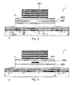
- FIGS 1A and B illustrate a hybridized grating-mirror vertical-cavity laser (VCL) structure as well as a method for hybridising a grating-mirror vertical-cavity laser (VCL) structure on a silicon platform, according to preferred embodiments of the present invention.
- VCL hybridized grating-mirror vertical-cavity laser
- FIG. 1A a hybridised VCL structure 1 is shown, comprising a partial VCL structure 2 and a silicon platform substrate 3.
- the partial VCL structure 2 comprises a highly reflective top mirror 4, here embodied by a distributed Bragg reflector (DBR) being a stack of alternating layers with different refractive indices.
- DBRs are commonly used top mirrors for VCSEL and their reflectivity can be finely tuned, and can be formed in III-V materials as well as other materials including SiO 2 .
- the top mirror serves as the out-coupling mirror, and typically has a reflectivity higher than 99% but lower than the reflectivity of a bottom mirror.
- the top mirror is not used as an out-coupling mirror and should therefore be highly reflecting.
- Such highly reflective top mirror 4 of the hybrid VCL preferably has a reflectivity larger than 99.5%, such as larger than 99.9%, such as 99.95%.
- the optimal value of the reflectivity of top mirror 4 should be determined considering the reflectivity of the grating mirror 12, one pass gain in the quantum wells (QWs), and the targeted differential quantum efficiency.
- the partial VCL structure 2 further comprises an active region 5 formed in III-V materials.
- the active region 5 can be formed as any applicable VCSEL active region, and typically comprises a series of epitaxially grown III-V material layers.
- a typical design includes upper and lower confinement layers sandwiching a QW structure 6 consisting of alternating QW layers (e.g. InAlGaAs or InGaNAs for wavelengths longer than > 1.3 ⁇ m, and GaAs for 850-nm wavelength) and barriers.
- the partial VCL structure 2 can in one embodiment be provided by a standard VCSEL structure, excluding the bottom mirror and with a highly reflective top mirror.
- electric contacts 8a and 8b are situated just above and just below the active region 5.
- This contact scheme is called intra-cavity contact.
- the top mirror 4 can be undoped. If necessary, the electric contact 8a can be made on top of the top mirror 4.
- This contact scheme is called extra-cavity contact. In the extra-cavity contact case, the top mirror should be appropriately doped.
- the optical confinement is provided by a current aperture formed by proton implantation, so that the optical mode is defined by the thermal lensing effect.
- the region 7 implanted by protons becomes insulating, working as a current aperture and defining the gain region 101.
- the gain region 201 is defined by the proton implanted region 202 while the optical mode is defined by the dielectric aperture 203 in the top mirror 4.
- the dielectric aperture is preferably formed by oxidation of a layer with high aluminium content.
- a layer with high aluminium content should be provided to the position where the dielectric aperture is to be formed when the mirror 4 is prepared.
- both optical gain region 301 and optical mode are defined by the dielectric aperture 303, preferably an oxide aperture formed in the active region.
- dielectric aperture 303 it is preferred that one.of layers between the upper contact 8a and the QW region 6 should have a high aluminium content for oxidation.
- the top mirror is an undoped DBR which can be expitaxially grown with the active region, wafer-bonded to the active region, or deposited on top of the active region.
- both optical gain region 401 and optical mode are defined by the dielectric aperture 403.
- the proton implanted region 402 is advantageous for high speed operation.
- the optical gain region 501 is defined by the tunnel junction 503 while the optical mode being defined by tunnel junction 503 and the thermal lensing effect.
- a tunnel junction highly n-doped and p-doped thin layers are put together, and the current flows only through this junction.
- the embodiment can have intra-cavity air gaps 507 for further tuning of the optical confinement.
- the top mirror is p-doped DBR which is preferably expitaxially grown with the active region.
- An oxide aperture (203) is formed by oxidizing a high aluminium content layer for both optical and gain confinements. This structure can be realized with GaAs latticed matched materials.
- the optical confinement is provided by vertically-shifted parts 703 of the DBR and the gain confinement by proton implanted region 707.
- the top DBR 4 is deposited after making shallow intra-cavity air gaps to form the vertically-shifted parts 703.
- This structure can be realized with InP or GaAs lattice matched materials.
- the P contact layer 709 is preferably highly absorbing InGaAs.
- the central of the P contact layer 709 is preferably removed. In the case of GaAs lattice-matched materials, this removal is not required.
- Figure 7A shows the hybrid VCL with a low index oxide layer 15', and 7B with a low index air gap 15" formed using an oxide spacer layer or mesa 715.
- the silicon platform substrate 3 is preferably a silicon-on-insulator (SOI) substrate consisting of a silicon substrate with a supporting layer 9 (typically SiO 2 ) topped by a silicon layer 10. Other configurations are possible, but it is preferred that the silicon layer is supported by a layer with lower refractive index as is the case here.
- SOI silicon-on-insulator
- the SOI substrate also holds integrated photonic and electric circuitry.
- the photonic circuitry including grating region 11 is formed using matured and precise silicon processing technologies such as complementary metal-oxide-semiconductor (CMOS) processing techniques, at the same time the electrical circuitry is formed using the same technologies.
- CMOS complementary metal-oxide-semiconductor
- the grating region 11 comprising a 1D or 2D periodic refractive index grating 12 formed by silicon layer parts 13 and regions 14 formed in the silicon layer which have a refractive index lower than the refractive index of the silicon layer.
- the regions 14 may be formed by removing the silicon layer in those regions, e.g. by matured silicon processing techniques, to form holes. The holes can be left empty, or could potentially be filled with a low-index material if this can be done without destroying the silicon parts 13. In an alternative approach, the regions 14 are formed by other modification of these regions of the silicon layer.
- the patterning and periodicity of the parts 13 and regions 14 of the periodic refractive index grating 12 will be described in more detail later in relation to Figures 13 and 14 .
- the silicon layer 10 is supported by a layer with lower refractive index, in this case the SiO 2 layer 9.
- the layer above the silicon layer 10 also has a lower refractive index. It is preferred to sandwich the grating region 11 between layers of lower refractive indices for gaining a high reflectivity from the grating region 11.
- a gap 15 between the silicon layer 10 and the partial VCL structure 2 is filled by material having a lower refractive index than silicon.
- such low index gap is provided by an oxide layer 15'.
- the oxide layer 15' is preferably provided on the partial VCL structure 2 prior to assembly, as shown in Figure 9A.
- Figures 9B and 9C show the front and right cross-sectional profile of bonded wafers, respectively.
- the GMVCL involves a structuring that forms an air gap 15" above the grating region 11.
- the structuring can be mesas 25 surrounding the grating region.
- the mesa 25 is preferably provided on the silicon layer 10 prior to assembly in order to avoid aligning during the wafer bonding.
- Figures 10B and 10C show the front and right cross-sectional profile of bonded wafer, respectively.
- ⁇ top and ⁇ grat are reflection phase shift from the top mirror and the bottom grating mirror.
- n eff is effective refractive index of the VCL cavity.
- the periodic refractive index grating 12 surrounded by lower index layers 9 and 15 establishes a high index contrast grating-mirror which functions as a bottom mirror for the hybrid VCL, and a VCL cavity is thereby formed between the periodic refractive index grating 12 and the top mirror 4.
- the regions 14 are preferably larger than the lateral extension of the vertically-resonant mode 16 to provide high reflectivity.
- the thickness of the periodic refractive index grating 12 can be that of the silicon layer 10, but may also be made smaller by selective etching of the grating region 11. The preferred values of key designing parameters of the grating mirror such as thickness, periodicity, and air filling ratio are described later.
- the supporting layer 9, here SiO 2 serves to vertically confine light to the grating region 11 and therefore preferably has a lower refractive index.
- the VCL cavity supports a vertically resonant mode symbolised by arrow-loop 16.
- Arrow 17 symbolises a laterally-propagating slow light mode of the grating.
- This slow light mode is an Eigen mode of the periodic refractive index grating 12.
- the light in the mode 16 is diffracted when incident to the grating; the part of diffracted light is coupled to the mode 17; the light in the mode 17 is coupled back to the mode 16.
- This coupling process may bring resonance, leading to a high reflectivity.
- the number of modes 17 involved in the coupling can be one or plural, depending on the design. No coupling loss is expected provided that the whole grating region is exactly periodic.
- the hybridised structure as described above serves the function of efficiently providing light in in-plane modes on a silicon platform. Below coupling the light in the slow light mode 17 to the laterally oriented out-coupling waveguide, and further to photonic circuitry or similar in the silicon platform, is described.
- light is coupled to an index contrast waveguide (ICWG) 19 formed in the silicon layer 10 to be connected to the grating region 11, preferably through an intermediate grating waveguide (GWG) 18 formed within the grating region 11 as shown in Figure 1B .
- ICWG index contrast waveguide
- GWG intermediate grating waveguide
- the light is coupled directly to an ICWG 19 formed to be connected to the grating region as illustrated in Figure 1C .
- light is coupled only to a GWG 18 formed within the grating region 11 as illustrated in Figure 1D .
- the GWG 18 can be constituted by a line defect in the periodic refractive index grating 12 of the grating region 11 and supports a laterally-propagating GWG mode 20 as shown in Figures 1A and 1B .
- the GWG 18 should be arranged to have some overlap with the lateral extension of the vertically-resonant mode 16 determined by the active region 101 as illustrated by the circle 16a in Figure 1B . Then, a part of light can be extracted from the PBG mode 17 to the GWG mode 20.
- the shape of GWG 18 can be optimized for efficient extraction. This issue will be described further later in relation to Figure 16 .
- the ICWG 19 is preferably a ridge waveguide formed outside the grating region by removing parts of the silicon layer by photolithography and etching.
- the ICWG 19 supports laterally-propagating ICWG mode 21 and is arranged to abut grating region at the end of the GWG 18. Then, the GWG mode 20 from the GWG 18 converts to ICWG mode 21.
- the ICWG 19 can connect to and form part of photonic circuitry on the silicon platform.
- the connecting part between the GWG 18 and the ICWG 19 can be can be optimized for better conversion efficiency. This issue will be described further in relation to Figure 16 .
- the building blocks of the hybrid VCL 1 can in preferred embodiments comprise:
- the hybrid VCL is a tunable hybrid laser.
- the top grating mirror (806) can be movable by using electrostatic force (described in more detail in Optics Express 15, 1222 (2007 )), piezoelectric force (described in more detail in IEEE J. Selected Topics in Quant. Electron. 13, 374 (2007 )), or thermally-induced strain (described in more detail in IEEE Photon. Technol. Lett. 18, 688 (2006 )) by applying voltage or current through a tuning contact 809.
- the movable top grating mirror can be replaced with a DBR or a mixture of grating and DBR. As the thickness of the tuning air gap changes, the emission wavelength of laser also can be varied.
- the fabrication of the partial VCL structure 2 as described in the above is considered within the realms of the person skilled in the art of VCSEL fabrication.
- the fabrication of the grating region 11 in the silicon platform substrate 3 is based on matured, precise, and cheap standard silicon processing technologies, which will typically be done simultaneously with the fabrication of electrical circuitry on the same silicon platform substrate 3.
- the partial VCL structure 2 is arranged on the silicon platform substrate 3 so that there is an overlap between transversal optical mode confinement in the GMVCL (defined by vertically-shifted DBR region 703, by the dielectric aperture, by the thermal lensing effect, or by the lateral extension of the top mirror 4) and the grating region 11.
- the proton implantation is performed during the typical processing of hybrid VCL after the wafer bonding, as described in Figure 9 .
- the position of proton implanted region 202 can be defined to be in alignment with both the grating region 11 and the GWG 18. Thus, no aligning effort is necessary for the wafer bonding.
- the proton implantation and oxidation is performed during the typical processing of hybridised VCL after the wafer bonding.
- the positions of proton implanted region 202 and dielectric aperture 203 can be defined to be in alignment with both the grating region 11 and GWG 18. Thus, no aligning effort is required for the wafer bonding.
- the dielectric aperture is formed using oxidation during the typical processing of hybridised GMVCL after the wafer bonding.
- the position of dielectric aperture 303 can be defined to be in alignment with both the grating region 11 and the GWG 1. Thus, no aligning effort is required for the wafer bonding.
- the proton implantation and the oxidation for the dielectric aperture 403 is performed during the typical processing of hybridised VCL after the wafer bonding.
- the positions of proton implanted region 402 and the dielectric aperture 403 can be defined to be in alignment with both the grating region 11 and GWG 18. Thus, no aligning effort is required for the wafer bonding.
- the tunnel junction 503 is formed by re-growth technique during epitaxial growth of the partial VCL epi structure 2'. Aligning the tunnel junction 503 with the grating region 11 and GWG 18 is necessary when bonding the partial VCL epi structure 2' and silicon platform substrate 3.
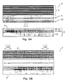
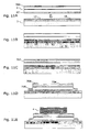
- FIG. 11A-E A fabrication flow for the hybrid VCL of Figure 7A is illustrated in Figures 11A-E .
- the active region 5 with an oxide gap 15' deposited and the silicon-based grating mirror 12 with a waveguide 18, are separately prepared. Then, they are wafer-bonded, as shown in Figure 11B .
- proton implanted regions 707 are formed as shown in Figure 11C .
- mesas are defined, the central part of the highly absorbing P contact layer 709 is removed, shallow trenches 704 for the formation of vertically-shifted DBR are etched, and metal contacts 708 are formed, as shown in Figure 11D .
- a top DBR is deposited, as shown in Figure 11E . No alignment is required in wafer bonding level. All other aligning precision is determined by photolithography resolution that is sufficient for most of applications.
- Figures 12A and B show part of a fabrication flow for the hybrid VCL of Figure 7B .
- the flow is similar to the one described in Figure 11A-E, except that no low index oxide layer is deposited on the active region 5, but instead a mesa 715 is formed on the substrate 3 to produce low index air gap 15" (12B).
- the periodicity, thickness, refractive index, and air filling ratio of grating mirror determines the dispersion of PBG modes of the grating mirror layer.
- possible ranges of the aforementioned design parameters of grating mirror are listed. Any other value can be also used if it leads to desirable Eigen mode dispersion.
- the periodicity of grating pattern ranges from 0.4 ⁇ to 0.8 ⁇ where ⁇ is the lasing wavelength of interest.
- the optical thickness of a grating layer can ranges from 0.6 ⁇ to 1.6 ⁇ .
- the optical thickness of a layer is defined as the physical thickness of the layer multiplied by the refractive index of the layer.
- the air filling ratio ranges from 20% to 70%.
- the air filling ratio is defined as a fraction of air (or other low index material) area 14 among the area of one grating period (13+14).
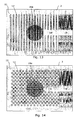
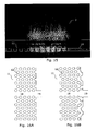
- Figure 15 shows a time frame from this dynamic simulation, where white and black indicate high and low electromagnetic (EM) field intensities, respectively.
- the design of the simulated device was similar to that shown in Figure 3 , and Figure 15 also indicates approximate positions of the partial VCL structure 2, the grating region 11 and the ICWG 19 in the silicon layer.
- the extraction of light from the PBG mode 17 in periodic grating region 12 to GWG mode 20 in GWG 18 can be further optimized to reduce undesirable coupling loss.
- the connecting part 28 in Figure 1B can be topologically optimized to minimize the scattering loss due to the breaking of periodicity of grating.
- the shape of GWG 18 can be optimized so that the dispersion of GWG mode 20 should be similar as that of PBG mode 17 for better mode matching.
- the efficiency of mode conversion from GWG mode 20 in GWG 18 to ICWG mode 21 in ICWG 19 also can be maximized by topologically optimizing the connecting part 30 in Figure 1B or C .
- a schematic example of topological optimization is shown in Figure 16.
- Figures 16A and 16B shows the connecting part 30 before and after the optimization, respectively.
Description
- The present invention relates to providing light to photonic circuits on a silicon platform that is compatible with matured silicon processing technologies. In particular, the invention relates to providing light to such circuitry by use of a grating-mirror vertical-cavity laser.
- The challenge of integrating small and efficient electrically pumped light sources in silicon based photonic circuitry is well known.
- Gunn (Photonics Spectra March 2006, pp. 62-67) described this challenge and proposes a solution where light is provided from non-integrated external laser sources. Through an optical fibre, the light is directed to an integrated holographic lens and thereby coupled to an integrated waveguide. This approach has the disadvantages that tedious alignment and subsequent packaging is necessary.
- Fang et al. (Optics Express 14, pp. 9203 (2006)) describes an edge-emitting electrically pumped AlGaInAs-silicon evanescent laser architecture. The architecture is wafer bonded to a silicon on insulator (SOI) substrate and the laser cavity is defined solely by a silicon waveguide in the underlying SOI substrate. An edge emitting distributed Bragg reflector (DBR) laser is disclosed in
WO 2008/068209 which also couples to a silicon waveguide. While solutions based on edge-emitting lasers provides easier coupling to photonic circuitry, they have the disadvantages of relatively high power consumption and non-intrinsic single mode control. - Ferrier L. et al.: "Vertical microcavities based on photonic crystal mirrors for III-V/Si integrated microlasers"; Proc. of the SPIE Vol. 6989, 2008, pages 69890W-1 - 69890W-12 discusses a number of setups related to vertical microcavities using photonic crystal (PhC) mirrors and coupling to lateral waveguides.
- Hence, an improved way of integrating light sources on silicon platforms would be advantageous, and in particular a more efficient and/or reliable ways of providing light to photonic circuits would be advantageous.
- It is an object of the present invention to provide an alternative to the prior art.
- In particular, it may be seen as an object of the present invention to provide a method and a hybrid vertical-cavity laser (hybrid VCL) structure that solve the above mentioned problems of the prior art with providing light to photonic circuits.
- Thus, the above described object and several other objects are intended to be obtained in a first aspect of the invention by providing a method for making various hybrid VCL structure on a silicon platform using a bottom grating mirror in the silicon platform, the method comprising:
- providing a layered structure comprising an active region formed in III-V materials and a highly reflective top mirror;
- forming a grating region in a silicon layer supported by a layer with lower refractive index than the silicon layer, the grating region comprising a one-dimensional (1D) or two-dimensional (2D) periodic refractive index grating formed by silicon layer parts and regions being formed in the silicon layer and having lower refractive indices than the silicon layer;
- forming a waveguide in the silicon layer, the waveguide being formed with an end part formed within or abutting the grating region to facilitate lateral out-coupling of light from the grating region to the waveguide, this may be obtained by forming the waveguide within and/or to be connected to, such as abutting, the grating region; and
- arranging the layered structure on the grating region, comprising providing a layer with a refractive index lower than the refractive index of the silicon layer between the layered structure and the grating region, whereby the periodic refractive index grating establishes a bottom grating mirror to form a VCL cavity between the top mirror and the grating region. The waveguide is preferably laterally oriented with respect to the VCL cavity and functions as an out-coupling waveguide for the VCL.
- In the following, a number of further aspects, preferred and/or optional features, elements, examples and implementations will be described. Features or elements described in relation to one embodiment or aspect may be combined with or applied to the other embodiments or aspects where applicable. For example, structural and functional features applied in relation to the hybrid VCL structure may also be used as features in relation to the method for hybrid VCL structure by proper adaptation and vice versa. Also, Explanations of underlying mechanisms of the invention as realized by the inventor are presented for explanatory purposes, and should not be used in ex post facto analysis for deducing the invention.
- The structure comprising the highly reflective top mirror, the active region and the bottom grating-mirror is referred to both as a "grating mirror vertical-cavity laser (GMVCL) structure" and as a VCL structure with, or formed using, a bottom grating-mirror. Within the meaning of the present description, these terms have the same meaning. Also, The layered structure comprising the highly reflective top mirror and the active region, but without the bottom grating mirror, is referred to as a "partial VCL structure" or simply the "layered structure", depending on the context.
- The hybrid VCL structure emits light laterally to the in-plane waveguide while the vertical-cavity surface-emitting laser (VCSEL) emits vertically from a mirror surface to the air. Hence, the hybrid VCL is a structure comprising a top mirror being highly reflective so as not to function as an output coupler, an active region formed in III-V materials, and a silicon-based grating region forming a highly reflective bottom grating-mirror for creating a VCL cavity with the top mirror, as well as a laterally oriented waveguide for emission of light from the VCL cavity to the outer photonic circuit in the silicon substrate.
- An example of a prior art VCSEL using two dimensional (2D) grating mirrors can be found in e.g.
US 2007/0201526 . This structure differs from the present invention in several ways, one of them being that one of the end mirrors has a reduced reflectivity in order to function as an output coupler, making the laser surface emitting. Further,US 2007/0201526 provides no in-plane waveguide structure in the layer holding the 2D grating structure intended to laterally output light. Nonetheless, the technology is similar and extensive references to VCSEL technology is made throughout the present description. The invention is thereby also advantageous as it applies matured VCSEL technologies exhibiting very low power consumption, eminent single-mode property and mode control in general. Further, the use of VCSEL technology allows for uncomplicated packaging. - It is preferred that the ways of obtaining optical and electrical confinement in the partial VCL structure provide relaxed alignment tolerance during the hybridisation, i.e. they do not rely on the exact positioning of the partial VCL structure on the bottom grating mirror, or in other words, the bottom grating mirror does not contribute or play a role in the obtaining of optical and electrical confinement.
- The top mirror is not used as an out-coupling mirror as in regular top-emission type VCSELs, and therefore has a higher reflectivity than normal out-coupling mirrors of VCSELs. It is preferred that the top mirror has a reflectivity as close to 100% as possible, e.g., higher than 99.95% in the case of absence of doping. The top mirror may be a distributed Bragg reflector (DBR), a grating mirror, a mixture of these two, or any other type of reflector. The top mirror can be epitaxially grown together with the active region, wafer-bonded to the active region, or deposited on to the active region, depending on the choice of materials and the method of obtaining optical and electrical confinements.
- The invention applies a grating mirror as the bottom reflector to establish the VCL cavity and as a router or coupler to deliver a fraction of incoming light to the in-plane waveguide. Highly reflective grating mirrors can be categorized into two types, according to the reflection mechanism. In one type, the resonance coupling of incident vertically-propagating free-space modes and laterally-propagating photonic bandgap (PBG) modes of grating is involved in the reflection process, while it is not in the other type. Even though both types can provide a reflectivity close to 100%, only the PBG mode-involved type can function as both a reflector and a router/coupler, and is thus the one preferably applied in the present invention. In this grating mirror type, the light in the incident free space mode is diffracted in the grating; part of the diffracted light is coupled to the preferably Γ (gamma) -point slow light PBG mode; the light in the PBG mode propagates laterally in the grating and is coupled back to the free space mode. This coupling process may result in resonance. In the absence of the in-plane waveguide within or connected to the grating mirror, this resonance coupling process can result in a reflectivity close to 100%. If an out-coupling waveguide is formed within and/or to be connected to the grating region, the PBG mode of the grating can be feasibly coupled to the waveguide mode; this provides a high routing/coupling efficiency of e.g., about -3 dB which is comparable to the coupling efficiency of a state-of-the-art holographic grating coupler. However, in the other type of grating mirror not involving PBG modes, the light in the free space mode is diffracted in the grating but is not as strongly coupled to the PBG mode; thus, routing efficiency is lower.
- The waveguide, also referred to as the in-plane, out-coupling waveguide, is formed in the silicon layer and preferably comprises a grating waveguide (GWG) in the grating region and an index contrast waveguide (ICWG) outside the grating region. The GWG is an intermediate waveguide to facilitate extracting fraction of light from PBG mode to ICWG mode. By optimizing the topology of GWG and the connecting part of GWG and ICWG, the routing efficiency can be further increased higher than -3dB. It is preferred that the bottom grating mirror with a lateral waveguide has a reflectivity of about 99.5 % and a routing efficiency of -3dB. This reflectivity value is comparable to the reflectivity of a vertically outputting mirror of the regular VCSELs.
- The routing function of the grating mirror is quite different from the coupling function of regular grating couplers. In the grating mirror of the present invention, a very small fraction of incident light is routed to the in-plane waveguide while most of incident light is reflected. For example, 99.5% of the incident light is reflected while 0.25 % is output to the waveguide, when the grating mirror has a reflectivity of 99.5% and a routing efficiency of -3dB. On the contrary, in a state-of-the-art holographic grating coupler, -3dB, i.e., 50 % of the incident light is coupled to the waveguide (Photonics Spectra March 2006, pp. 62-67).
- This combination of a highly reflective grating mirror involving resonance coupling with PBG modes and an in-plane output coupler in the form of the waveguide formed within or to be connected to the grating region is new. Most of seemingly-similar grating structures reported so far, are different from the grating mirror of the present invention in the aspects of structural shape, function, or reflection process (involvement of slow light modes). For example:
- in
US 2007/0153860, I.-S. Chung et al. ("Subwavelength Grating-Mirror VCSEL With a Thin Oxide Gap", IEEE Photonics Technology Letters, 2 (2008) 20, pages 105 - 107), andWO 2005/089098 , the reflection do not involve resonance coupling with slow light PBG modes; - In
US 6,031,243 , the grating does not work as a reflector; - In
US 2007/0201526 , the grating mirror has no waveguide connected for lateral output and the slow light PBG mode locates far from the r (gamma) point in the dispersion diagram; - In R. Jones et al. ("Grating based hybrid silicon lasers", Proceedings of SPIE, vol. 7230, pp 72300U-1), the grating is used to select a lasing frequency, and does not function as reflector nor router;
- In H. Wu et al. ("Ultra broadband SOI binary blazed grating mirror", 5th IEEE International Conference on Group IV Photonics, pp 299-301), the grating is surface grating, i.e., the bottom of the grating is not supported by a lower refractive index material. Thus, its reflectivity does not exceed 99% which is insufficient for lasing.
- The invention is particularly, but not exclusively, advantageous for providing light to photonic circuits using a hybrid VCL structure that is hybridised on a silicon platform in a way that is less sensitive to aligning error than many prior art solutions. This is advantageous as it provides for an easier and thereby cheaper alignment during assembly of the different parts.
- The invention is also advantageous as it applies one dimensional (1D) or two dimensional (2D) passive grating and preferably also a grating waveguide. In the literature, 2D grating and grating waveguide are often called photonic crystal (PhC) and photonic crystal waveguide (PhCWG), respectively. To avoid confusion, hereafter, PhC and PhCWG are called 2D grating and GWG, respectively.
- Hybridising is the act of mixing different species or varieties to produce hybrids. In the present context, it means connecting, physically and functionally, structures formed in materials from group III and V in the periodic table of the elements (hereafter group III-V materials) with structures formed in group IV materials. Similarly, a hybridised structure is a structure formed in group III-V materials connected to a structure formed in group IV materials, or vice versa. The connection is typically made by wafer bonding techniques, and it is preferred that the III-V active region of the partial VCL structure is wafer-bonded to the silicon-based grating region. Other connecting techniques also can be utilized if adequate for the application of interest.
- In the following, the term hybridised VCL means the structure obtained when the layered structure comprising the highly reflective top mirror and the active region (group III-V materials) are connected to the grating region (group IV materials). The establishment of this connection provides both a VCL (as the grating region provides the bottom mirror) and a hybridised structure in accordance with the above definitions. However, for the sake of ensuring compliance with other well established terms in the field, a "hybrid VCL" is also referred to as a "hybridised VCL structure" with the specification that this is done using a grating mirror. Within the meaning of the present description, this has the same meaning.
- As the person skilled in the art will understand, the silicon layer may be several separated silicon layer parts arranged on a substrate, some parts potentially in different levels. Also, it will be understood that although silicon is the preferred method of the current technology, other materials, such as other type IV-materials, IV material compositions, or high-refractive-index material, exhibiting similar properties may substitute silicon in respect of the present invention.
- In a second aspect, the invention provides a hybridised VCL structure comprising:
- a layered structure comprising an active region formed in group III-V materials and a highly reflective top mirror that is not used as an out-coupling mirror and that has a reflectivity preferably higher than 99.95%; and
- a grating region formed in a silicon layer supported by a layer with lower refractive index, the grating region comprising a 1D or 2D periodic refractive index grating formed by silicon layer parts and regions being formed in the silicon layer and having refractive indices lower than the refractive index of the silicon layer;
- a layer with refractive Index lower than the refractive index of the silicon layer provided on top of the grating region of the silicon layer;
where the layered structure is arranged on the grating region so that the periodic refractive index grating establishes a bottom grating-mirror forming a VCL cavity between the top mirror and the grating region, the bottom grating-mirror also facilitating coupling of light in vertical modes of the VCL cavity to in-plane modes of the grating region, and - a waveguide formed in the silicon layer and having an end part formed within or abutting the grating region to facilitate coupling of light from the grating region to the waveguide.
- A third aspect relates to the silicon-based substrate with grating region from the second aspect, but provided alone. Thus, in a third aspect, the invention provides a silicon-based grating mirror with a laterally oriented waveguide comprising
- a silicon layer being supported by a layer with lower refractive index;
- a grating region comprising a 1D or 2D periodic refractive index grating formed by silicon layer parts and regions being formed in the silicon layer that have refractive indices lower than the refractive index of the silicon layer;
- at least part of the grating region forming a grating-mirror for reflecting normally incident light and couple normally incident light to in-plane modes of the grating region; and
- a waveguide formed in the silicon layer and having an end part formed within or abutting the grating region to facilitate coupling of light from in-plane modes of the grating region to the waveguide.
- Any layer formed on top of the grating region, such as the low index layer, is transparent for lasing wavelength. For example, the lasing wavelengths can be 1.1, 1.3, and 1.55 µm.
- During fabrication processing of the device, the reflectivity of the grating mirror can be adjusted by lithographically changing the grating design, i.e., thickness, periodicity, air filling ratio, and pattern shape of the grating, while the lasing wavelength of the GMVCL may be adjusted by changing the thickness of a low index layer above the silicon grating.
- In a fourth aspect, the partial VCL structure and substrate with grating region from the second aspect are provided together as individual, unassembled structures. Hence, in the fourth aspect, the invention provides a partial VCL structure as described in the second aspect and a silicon layer as described in the second aspect, but as a kit for assembly instead of a connected structure.
- Additionally or alternatively, the fourth aspect may provide a layered structure and a silicon layer for receiving the layered structure;
- the layered structure comprising an active region formed in group III-V materials and a highly reflective top mirror that is not used as an out-coupling mirror and that has a reflectivity close to 100 %, e.g., higher than than 99.95%;
- the silicon layer comprising
- o a silicon layer being supported by a layer with lower refractive index than the silicon layer;
- o a grating region comprising a 1D or 2D periodic refractive index grating formed by silicon layer parts and regions being formed in the silicon layer and having refractive indices lower than the refractive index of the silicon layer; and
- o a waveguide formed in the silicon layer and arranged to facilitate coupling of light from the grating region to the waveguide;
- In some embodiments, the GWG in the grating region may be omitted so that the coupling is directly from the in-plane PBG mode of the periodic refractive index grating to a waveguide formed outside the grating region, such as an index contrast waveguide. This may, however decrease the coupling efficiency.
- It is preferred that an embodiment of the method comprises coupling of light from the VCL cavity to in-plane PBG modes of the grating region. The hybridised structure thereby serves the function of efficiently providing light to in-plane grating modes in a silicon layer, which is advantageous for providing light to a photonic circuit on a silicon platform.
- The coupling to the ICWG may be facilitated through an intermediate GWG, preferably formed within the grating region. In this embodiment, it is preferred that an embodiment of the method further comprises coupling of light from the in-plane PBG modes of the grating region to waveguide modes of a GWG formed in the silicon layer, preferably within the grating region. This arranging may be realised by ensuring a partial overlap between the GWG and VCL cavity modes in the bottom grating-mirror appearing when the VCL emits light and by designing the geometry of GWG so that the mode dispersion of GWG modes be similar as or adiabatically being transformed to that or those of the PBG modes.
- Optimizing the topology of the GWG and the connecting part of GWG and ICWG may be preferred in order to further decrease the unwanted scattering loss during the mode coupling/routing, increasing the overall routing efficiency.
- It is further preferred that definition of an optical gain region of the VCL is performed after arranging of the partial VCL structure on the silicon layer. This provides the advantage that the optical gain region can be defined to have the desired overlap with the periodic refractive index grating after the assembly, typically performed by wafer bonding, where they do no more move in relation to each others. This means that little or no aligning effort is necessary during the assembly. The position of the optical gain region of the VCL involves defining a current aperture or similar for directing charge carriers to a delimited part of the active region of the VCL structure.
- The present invention provides a light source for photonic circuits on a silicon platform in a cheap, compact and efficient way. The basic idea of the invention is to form a vertical laser cavity between a top mirror and a active region based on standard VCSEL technology, and a bottom mirror being a refractive index grating-mirror formed in a silicon layer on a substrate. The grating mirror in the silicon layer is so designed that the reflection process in the grating mirror includes the conversion of vertical resonant mode to in-plane PBG modes of the grating mirror. By providing coupling of the in-plane PBG modes to an in-plane waveguide, light can be provided to e.g. in-plane photonic circuits on a SOI/CMOS substrate. All the fabrication process can be performed using matured III-V VCSEL technology and silicon technology.
- These and other aspects of the invention will be apparent from the following description with reference to the described embodiments. Embodiments of the invention are defined in claims 1 - 13.
- Embodiments of the invention will now be described in more detail with regard to the accompanying figures. The figures show one way of implementing the present invention and is not to be construed as being limiting to other possible embodiments failing within the scope of the attached claim set.
-
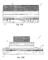
Figures 1 is schematic illustrations of a hybridised VCL on a SOI substrate according to an embodiment of the invention.Figures 1A shows the assembled structure in a profile view.Figure 1B ,1C and 1D show the SOI substrate from a top view, illustrating areas of further optimization and different embodiments for the waveguide. -
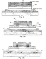
Figures 2-7 show four different confinement schemes for optical mode confinement and gain/electrical confinement. -
Figure 8 shows a tunable hybrid VCL according to an embodiment of the invention. -
Figures 9-12 schematically illustrate different assembly and fabrication schemes according to embodiments of the invention. -
Figures 13 and 14 show different layouts of grating regions in accordance with embodiments of the invention. -
Figure 15 is a frame from a dynamic (time-domain) numerical simulation of an embodiment of the invention. -
Figures 16A and B show examples of optimization of areas designated inFigure 1B . -
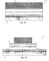
Figures 1A and B illustrate a hybridized grating-mirror vertical-cavity laser (VCL) structure as well as a method for hybridising a grating-mirror vertical-cavity laser (VCL) structure on a silicon platform, according to preferred embodiments of the present invention. - First, an assembled structure and operating principles are described in relation to
Figures 1A-C . InFigure 1A , a hybridisedVCL structure 1 is shown, comprising apartial VCL structure 2 and asilicon platform substrate 3. - The
partial VCL structure 2 comprises a highly reflectivetop mirror 4, here embodied by a distributed Bragg reflector (DBR) being a stack of alternating layers with different refractive indices. DBRs are commonly used top mirrors for VCSEL and their reflectivity can be finely tuned, and can be formed in III-V materials as well as other materials including SiO2. - For normal VCSELs, the top mirror serves as the out-coupling mirror, and typically has a reflectivity higher than 99% but lower than the reflectivity of a bottom mirror. In the present hybrid VCL, the top mirror is not used as an out-coupling mirror and should therefore be highly reflecting. Such highly reflective
top mirror 4 of the hybrid VCL preferably has a reflectivity larger than 99.5%, such as larger than 99.9%, such as 99.95%. The optimal value of the reflectivity oftop mirror 4 should be determined considering the reflectivity of thegrating mirror 12, one pass gain in the quantum wells (QWs), and the targeted differential quantum efficiency. - The
partial VCL structure 2 further comprises anactive region 5 formed in III-V materials. Theactive region 5 can be formed as any applicable VCSEL active region, and typically comprises a series of epitaxially grown III-V material layers. A typical design includes upper and lower confinement layers sandwiching aQW structure 6 consisting of alternating QW layers (e.g. InAlGaAs or InGaNAs for wavelengths longer than > 1.3 µm, and GaAs for 850-nm wavelength) and barriers. - The
partial VCL structure 2 can in one embodiment be provided by a standard VCSEL structure, excluding the bottom mirror and with a highly reflective top mirror. - The embodiment of the hybrid VCL shown in
Figure 1A ,electric contacts active region 5. This contact scheme is called intra-cavity contact. In the intra-cavity contact case, thetop mirror 4 can be undoped. If necessary, theelectric contact 8a can be made on top of thetop mirror 4. This contact scheme is called extra-cavity contact. In the extra-cavity contact case, the top mirror should be appropriately doped. - In the following, a number of possible ways of defining the position of the optical gain region and the optical mode in the GMVCL is described in relation to
Figures 1-7 . Elements of the GMVCL not described are assumed to be similar to those described above in relation toFigures 1A and B . - In the embodiment of the hybrid VCL shown in
Figure 1A , the optical confinement is provided by a current aperture formed by proton implantation, so that the optical mode is defined by the thermal lensing effect. Theregion 7 implanted by protons becomes insulating, working as a current aperture and defining thegain region 101. - In the embodiment of the hybrid VCL shown in
Figure 2 , thegain region 201 is defined by the proton implantedregion 202 while the optical mode is defined by thedielectric aperture 203 in thetop mirror 4. The dielectric aperture is preferably formed by oxidation of a layer with high aluminium content. Thus, a layer with high aluminium content should be provided to the position where the dielectric aperture is to be formed when themirror 4 is prepared. - In the embodiment of the hybrid VCL shown in
Figure 3 , bothoptical gain region 301 and optical mode are defined by thedielectric aperture 303, preferably an oxide aperture formed in the active region. For the formation ofdielectric aperture 303, it is preferred that one.of layers between theupper contact 8a and theQW region 6 should have a high aluminium content for oxidation. The top mirror is an undoped DBR which can be expitaxially grown with the active region, wafer-bonded to the active region, or deposited on top of the active region. - In the embodiment of the hybrid VCL shown in
Figure 4 , bothoptical gain region 401 and optical mode are defined by thedielectric aperture 403. The proton implantedregion 402 is advantageous for high speed operation. - In the embodiment of the hybrid VCL shown in
Figure 5 , theoptical gain region 501 is defined by thetunnel junction 503 while the optical mode being defined bytunnel junction 503 and the thermal lensing effect. In a tunnel junction, highly n-doped and p-doped thin layers are put together, and the current flows only through this junction. Optionally, the embodiment can haveintra-cavity air gaps 507 for further tuning of the optical confinement. - In the embodiment of the hybrid VCL shown in
Figure 6 , the top mirror is p-doped DBR which is preferably expitaxially grown with the active region. An oxide aperture (203) is formed by oxidizing a high aluminium content layer for both optical and gain confinements. This structure can be realized with GaAs latticed matched materials. - In the embodiment of the hybrid VCL shown in
Figures 7A and B , the optical confinement is provided by vertically-shiftedparts 703 of the DBR and the gain confinement by proton implantedregion 707. Thetop DBR 4 is deposited after making shallow intra-cavity air gaps to form the vertically-shiftedparts 703. This structure can be realized with InP or GaAs lattice matched materials. In the case of InP lattice-matched materials, theP contact layer 709 is preferably highly absorbing InGaAs. To avoid unwanted absorption, the central of theP contact layer 709 is preferably removed. In the case of GaAs lattice-matched materials, this removal is not required.Figure 7A shows the hybrid VCL with a low index oxide layer 15', and 7B with a lowindex air gap 15" formed using an oxide spacer layer ormesa 715. - The
silicon platform substrate 3 is preferably a silicon-on-insulator (SOI) substrate consisting of a silicon substrate with a supporting layer 9 (typically SiO2) topped by asilicon layer 10. Other configurations are possible, but it is preferred that the silicon layer is supported by a layer with lower refractive index as is the case here. Thesilicon platform substrate 3 is shown alone in a top-view inFigure 1B-D . - In a preferred embodiment, the SOI substrate also holds integrated photonic and electric circuitry. Preferably, the photonic circuitry including
grating region 11 is formed using matured and precise silicon processing technologies such as complementary metal-oxide-semiconductor (CMOS) processing techniques, at the same time the electrical circuitry is formed using the same technologies. - In the
top silicon layer 10 is formed agrating region 11 and awaveguide grating region 11 comprising a 1D or 2D periodic refractive index grating 12 formed bysilicon layer parts 13 andregions 14 formed in the silicon layer which have a refractive index lower than the refractive index of the silicon layer. Theregions 14 may be formed by removing the silicon layer in those regions, e.g. by matured silicon processing techniques, to form holes. The holes can be left empty, or could potentially be filled with a low-index material if this can be done without destroying thesilicon parts 13. In an alternative approach, theregions 14 are formed by other modification of these regions of the silicon layer. The patterning and periodicity of theparts 13 andregions 14 of the periodic refractive index grating 12 will be described in more detail later in relation toFigures 13 and 14 . - As mentioned previously, it is preferred that the
silicon layer 10 is supported by a layer with lower refractive index, in this case the SiO2 layer 9. Similarly, it is preferred that the layer above thesilicon layer 10 also has a lower refractive index. It is preferred to sandwich thegrating region 11 between layers of lower refractive indices for gaining a high reflectivity from thegrating region 11. - For this purpose, a
gap 15 between thesilicon layer 10 and thepartial VCL structure 2 is filled by material having a lower refractive index than silicon. In the embodiment shown inFigure 1A andFigure 9D , such low index gap is provided by an oxide layer 15'. The oxide layer 15' is preferably provided on thepartial VCL structure 2 prior to assembly, as shown inFigure 9A. Figures 9B and9C show the front and right cross-sectional profile of bonded wafers, respectively. In the embodiment shown inFigure 10D , the GMVCL involves a structuring that forms anair gap 15" above thegrating region 11. Here, the structuring can bemesas 25 surrounding the grating region. As shown inFigure 10A , themesa 25 is preferably provided on thesilicon layer 10 prior to assembly in order to avoid aligning during the wafer bonding.Figures 10B and10C show the front and right cross-sectional profile of bonded wafer, respectively. In order to avoid evanescent coupling, the thickness of oxide layer 15' orair gap 15" preferably has a minimum thickness of λ\/2ngap, where λ is the lasing wavelength of interest and ngap is the refractive index of oxide layer 15' orair gap 15". For typical applications with λ =1550 nm, this minimum thickness is about 500 nm for the oxide layer 15' and about 780 nm for theair gap 15". - By varying the thickness of oxide layer 15' or
air gap 15", the effective cavity length deff of the VCL cavity can be changed. This leads to the change of lasing wavelength λ that is determined by the following relation:
- Here, ϕtop and ϕgrat are reflection phase shift from the top mirror and the bottom grating mirror. The neff is effective refractive index of the VCL cavity. Thus, the lasing wavelength λ can be feasibly chosen during processing, which makes the hybrid VCL adequate for multi-wavelength source.
- The periodic refractive index grating 12 surrounded by
lower index layers top mirror 4. - The
regions 14 are preferably larger than the lateral extension of the vertically-resonant mode 16 to provide high reflectivity. The thickness of the periodic refractive index grating 12 can be that of thesilicon layer 10, but may also be made smaller by selective etching of thegrating region 11. The preferred values of key designing parameters of the grating mirror such as thickness, periodicity, and air filling ratio are described later. - The supporting
layer 9, here SiO2, serves to vertically confine light to thegrating region 11 and therefore preferably has a lower refractive index. To avoid undesirable evanescent coupling to silicon substrate, the supporting layer preferably has a minimum thickness of λ/2nsupp, where nsupp is the refractive index of the supporting layer. For typical applications at λ = 1550 nm and with the supporting layer being SiO2, this minimum thickness will be around 500 nm. - The origin of the high reflection of the bottom grating mirror is explained in terms of the modes involved. The involved modes are schematically drawn in
Figure 1A and 1B . First, the VCL cavity supports a vertically resonant mode symbolised by arrow-loop 16.Arrow 17 symbolises a laterally-propagating slow light mode of the grating. This slow light mode is an Eigen mode of the periodic refractive index grating 12. The light in themode 16 is diffracted when incident to the grating; the part of diffracted light is coupled to themode 17; the light in themode 17 is coupled back to themode 16. This coupling process may bring resonance, leading to a high reflectivity. The number ofmodes 17 involved in the coupling can be one or plural, depending on the design. No coupling loss is expected provided that the whole grating region is exactly periodic. - The hybridised structure as described above serves the function of efficiently providing light in in-plane modes on a silicon platform. Below coupling the light in the
slow light mode 17 to the laterally oriented out-coupling waveguide, and further to photonic circuitry or similar in the silicon platform, is described. - In a preferred embodiment illustrated in
Figure 1 , light is coupled to an index contrast waveguide (ICWG) 19 formed in thesilicon layer 10 to be connected to thegrating region 11, preferably through an intermediate grating waveguide (GWG) 18 formed within thegrating region 11 as shown inFigure 1B . In the alternative, the light is coupled directly to an ICWG 19 formed to be connected to the grating region as illustrated inFigure 1C . In another alternative light is coupled only to aGWG 18 formed within thegrating region 11 as illustrated inFigure 1D . - The
GWG 18 can be constituted by a line defect in the periodic refractive index grating 12 of thegrating region 11 and supports a laterally-propagatingGWG mode 20 as shown inFigures 1A and 1B . TheGWG 18 should be arranged to have some overlap with the lateral extension of the vertically-resonant mode 16 determined by theactive region 101 as illustrated by thecircle 16a inFigure 1B . Then, a part of light can be extracted from thePBG mode 17 to theGWG mode 20. The shape ofGWG 18 can be optimized for efficient extraction. This issue will be described further later in relation toFigure 16 . - The
ICWG 19 is preferably a ridge waveguide formed outside the grating region by removing parts of the silicon layer by photolithography and etching. TheICWG 19 supports laterally-propagatingICWG mode 21 and is arranged to abut grating region at the end of theGWG 18. Then, theGWG mode 20 from theGWG 18 converts toICWG mode 21. TheICWG 19 can connect to and form part of photonic circuitry on the silicon platform. The connecting part between theGWG 18 and theICWG 19 can be can be optimized for better conversion efficiency. This issue will be described further in relation toFigure 16 . - In summary, the building blocks of the
hybrid VCL 1 can in preferred embodiments comprise: - a top part being a
partial VCL structure 2 with- ○ A
top mirror 4. The top mirror can be a multi layer mirror so called distributed Bragg mirror (DBR), or a single layer grating mirror. They can be epitaxially grown on top of the active region, wafer-bonded to the active region, or deposited on top of the active region. - ○ An
active region 5. The active region can be InP or GaAs lattice matched materials. Other III-V semiconductors can be employed depending on the purpose of applications. - ○ Means for optical confinement. Optical confinement can be obtained in various ways such as vertically shifted DBR, oxide aperture, and thermal lensing as described in relation to
Figures 1-7 . - ○ Means for gain confinement. Gain confinement can be obtained in several ways such as proton implantation, oxide aperture, and tunnel junction as described in relation to
Figures 1-7 .
- ○ A
- A
low index gap 15. The low index gap can be oxide (or other low index material) or air. When the gap is an oxide layer 15', it is preferable that the oxide gap is deposited to the active before bonding, as illustrated inFigure 11A . In the case ofair gap 15", it is preferable that a spacer layer is deposited to the SOI before making the grating pattern, as illustrated inFigure 11A . - a
silicon platform substrate 3, such as a SOI substrate, with agrating region 11 forming- o a silicon-based
grating mirror 12, and - o a laterally out-
coupling grating waveguide 18,
- o a silicon-based
- Metal contacts. The metal contacts can be P and N contacts or N and N contacts, depending on the gain confinement apparatus. For example, when the implantation or oxide aperture is employed for the gain confinement, P and N contacts should be used. In the case of tunnel junction, N and N contacts should be used. Depending on designs, the top contact can be formed on top of the top mirror (extra-cavity contact scheme) or on top of the active (intra-cavity contact). In tunable lasers, an extra tuning contact is required, as illustrated in
Figure 8 . Optionally, the metal contacts are formed on highly doped contact layers. When the active consists of InP-lattice matched material and the P metal contact is required, the P contact layer is preferably highly absorbing InGaAs. Thus, part of this layer (107) needs to be removed to avoid unwanted absorption, as illustrated inFigures 7A andB and 11D. - The various embodiments illustrate different ways in which these building blocks can be combined. However, the described designs are not limited to these embodiments, but any other combinations are possible as long as they can be hybridised with a silicon-based grating mirror with a laterally oriented waveguide for out-coupling purposes.
- In the embodiment shown in
Figure 8 , the hybrid VCL is a tunable hybrid laser. The top grating mirror (806) can be movable by using electrostatic force (described in more detail inOptics Express 15, 1222 (2007tuning contact 809. The movable top grating mirror can be replaced with a DBR or a mixture of grating and DBR. As the thickness of the tuning air gap changes, the emission wavelength of laser also can be varied. - In the following, different embodiments of fabricating the hybridised VCLs according to some of the embodiments presented earlier will be described. First, a typical fabrication of the hybridised
VCL structure 1 is described in relation toFigure 2. - As the
partial VCL structure 2 is based on matured VCSEL technology, the fabrication of thepartial VCL structure 2 as described in the above is considered within the realms of the person skilled in the art of VCSEL fabrication. Similarly, the fabrication of thegrating region 11 in thesilicon platform substrate 3 is based on matured, precise, and cheap standard silicon processing technologies, which will typically be done simultaneously with the fabrication of electrical circuitry on the samesilicon platform substrate 3. - The
partial VCL structure 2 is arranged on thesilicon platform substrate 3 so that there is an overlap between transversal optical mode confinement in the GMVCL (defined by vertically-shiftedDBR region 703, by the dielectric aperture, by the thermal lensing effect, or by the lateral extension of the top mirror 4) and thegrating region 11. - In most of embodiments of hybrid VCL structure, arranging the partial VCL epi structure 2' in
Figure 9A onto thesilicon platform substrate 3 does not involve any significant aligning effort. No need of aligning for wafer bonding enables the mass production of hybrid VCL at a low fabrication cost. This feature is described in detail with embodiments of hybrid VCL structure shown inFigures 1-7 . - In the embodiment of hybrid VCL structure shown in
Figure 1A , the proton implantation is performed during the typical processing of hybrid VCL after the wafer bonding, as described inFigure 9 . The position of proton implantedregion 202 can be defined to be in alignment with both thegrating region 11 and theGWG 18. Thus, no aligning effort is necessary for the wafer bonding. - In the embodiment of hybrid VCL structure shown in
Figure 2 , the proton implantation and oxidation is performed during the typical processing of hybridised VCL after the wafer bonding. The positions of proton implantedregion 202 anddielectric aperture 203 can be defined to be in alignment with both thegrating region 11 andGWG 18. Thus, no aligning effort is required for the wafer bonding. - In the embodiment of hybrid VCL structure shown in
Figure 3 , the dielectric aperture is formed using oxidation during the typical processing of hybridised GMVCL after the wafer bonding. The position ofdielectric aperture 303 can be defined to be in alignment with both thegrating region 11 and theGWG 1. Thus, no aligning effort is required for the wafer bonding. - In the embodiment of hybrid VCL structure shown in
Figure 4 , the proton implantation and the oxidation for thedielectric aperture 403 is performed during the typical processing of hybridised VCL after the wafer bonding. The positions of proton implantedregion 402 and thedielectric aperture 403 can be defined to be in alignment with both thegrating region 11 andGWG 18. Thus, no aligning effort is required for the wafer bonding. - In the embodiment of hybrid VCL structure shown in
Figure 5 , thetunnel junction 503 is formed by re-growth technique during epitaxial growth of the partial VCL epi structure 2'. Aligning thetunnel junction 503 with thegrating region 11 andGWG 18 is necessary when bonding the partial VCL epi structure 2' andsilicon platform substrate 3. - The following describes the fabrication of the hybrid VCLs described in relation to
Figures 7A and B . The fabrication methods described here can be applied, or modified to be applicable to, the other embodiments described in relation toFigures 1-8 by the person skilled in the art. - A fabrication flow for the hybrid VCL of
Figure 7A is illustrated inFigures 11A-E . As illustrated inFigure 11A , theactive region 5 with an oxide gap 15' deposited and the silicon-basedgrating mirror 12 with awaveguide 18, are separately prepared. Then, they are wafer-bonded, as shown inFigure 11B . For gain confinement, proton implantedregions 707 are formed as shown inFigure 11C . Then, mesas are defined, the central part of the highly absorbingP contact layer 709 is removed,shallow trenches 704 for the formation of vertically-shifted DBR are etched, andmetal contacts 708 are formed, as shown inFigure 11D . Then, a top DBR is deposited, as shown inFigure 11E . No alignment is required in wafer bonding level. All other aligning precision is determined by photolithography resolution that is sufficient for most of applications. -
Figures 12A and B show part of a fabrication flow for the hybrid VCL ofFigure 7B . The flow is similar to the one described inFigure 11A-E, except that no low index oxide layer is deposited on theactive region 5, but instead amesa 715 is formed on thesubstrate 3 to produce lowindex air gap 15" (12B). - Different 1D, 2D, and modified 2D patterns of the periodic refractive index grating 12 of the
grating region 11 are shown inFigures 1B ,13 and 14 . In all three cases, the pattern should be periodic to have Eigen modes. As shown inFigure 14 , the shape of a single pattern might be made looking odd if necessary. - From ideal design point of view, the important thing is which pattern gives desirable PBG mode dispersion and the resultant mirror characteristics. From fabrication point of view, the mechanical stability of thin grating layer structure, the fabrication feasibility, and fabrication cost need to be considered to choose the pattern.
- The periodicity, thickness, refractive index, and air filling ratio of grating mirror determines the dispersion of PBG modes of the grating mirror layer. In the following, possible ranges of the aforementioned design parameters of grating mirror are listed. Any other value can be also used if it leads to desirable Eigen mode dispersion.
- The periodicity of grating pattern, either 1D or 2D, ranges from 0.4λ to 0.8λ where λ is the lasing wavelength of interest.
- The optical thickness of a grating layer can ranges from 0.6λ to 1.6λ. The optical thickness of a layer is defined as the physical thickness of the layer multiplied by the refractive index of the layer.
- The air filling ratio ranges from 20% to 70%. The air filling ratio is defined as a fraction of air (or other low index material)
area 14 among the area of one grating period (13+14). - A numerical simulation of the function of an embodiment of the present invention was performed.
Figure 15 shows a time frame from this dynamic simulation, where white and black indicate high and low electromagnetic (EM) field intensities, respectively. The design of the simulated device was similar to that shown inFigure 3 , andFigure 15 also indicates approximate positions of thepartial VCL structure 2, thegrating region 11 and theICWG 19 in the silicon layer. - As can be seen, there is a reasonable coupling from the vertical lasing modes (16 in
Figure 1A ) to the ICWG modes (21 inFigure 1A ). - As mentioned previously, the extraction of light from the
PBG mode 17 in periodicgrating region 12 toGWG mode 20 inGWG 18 can be further optimized to reduce undesirable coupling loss. The connectingpart 28 inFigure 1B can be topologically optimized to minimize the scattering loss due to the breaking of periodicity of grating. The shape ofGWG 18 can be optimized so that the dispersion ofGWG mode 20 should be similar as that ofPBG mode 17 for better mode matching. The efficiency of mode conversion fromGWG mode 20 inGWG 18 toICWG mode 21 inICWG 19 also can be maximized by topologically optimizing the connectingpart 30 inFigure 1B orC . A schematic example of topological optimization is shown inFigure 16. Figures 16A and 16B shows the connectingpart 30 before and after the optimization, respectively. - Examples of such topology optimization is described in e.g. L. Yang, et al., Electronic Letters, 13, p. 923 (2007), where 5 dB improvement in transmission is reported.
- Although the present invention has been described in connection with the specified embodiments, it should not be construed as being in any way limited to the presented examples. The scope of the present invention is to be interpreted in the light of the accompanying claim set. In the context of the claims, the terms "comprising" or "comprises" do not exclude other possible elements or steps. Also, the mentioning of references such as "a" or "an" etc. should not be construed as excluding a plurality. The use of reference signs in the claims with respect to elements indicated in the figures shall also not be construed as limiting the scope of the invention. Furthermore, individual features mentioned in different claims, may possibly be advantageously combined, and the mentioning of these features in different claims does not exclude that a combination of features is not possible and advantageous.
-
- Gunn, Photonics Spectra March 2006, pp. 62-67
- Fang et al. Optics Express, 14, pp. 9203 (2006)
-
US 2007/0153860 -
US 6,031,243 - I.-S. Chung et al., "Subwavelength Grating-Mirror VCSEL With a Thin Oxide Gap", IEEE Photonics Technology Letters, 2 (2008) 20, pages 105 - 107
-
US 2007/0201526 - R. Jones et al., "Grating based hybrid silicon lasers", Proceedings of SPIE, vol. 7230, pp 72300U-1 to 72300U-8.
-
WO 2005/089098 - H. Wu et al., "Ultra broadband SOI binary blazed grating mirror", 5th IEEE International Conference on Group IV Photonics, pp 299-301.
- Huang et al., )
- IEEE j. selected topics in Quant. Electron. 13, 374 (2007)
- IEEE Photon. Technol. Lett. 18, 688 (2006)
- L. Yang, et al., Electronic Letters, 13, p. 923 (2007)
-
WO 2008/068209 -
US 2007/0201526 - Ferrier L. et al.: "Vertical microcavities based on photonic crystal mirrors for III-V/Si integrated microlasers"; Proc. of the SPIE Vol. 6989, 2008, pages 69890W-1 - 69890W-12.
Claims (13)
- A method for hybridising a vertical-cavity laser VCL structure (1) on a silicon platform using a bottom grating-mirror in the silicon platform, the method comprising:providing a layered structure (2) comprising an active region (5) formed in III-V materials and a highly reflective top mirror (4) that is not used as an out-coupling mirror and that has a reflectivity larger than 99.5%;forming a grating region (11) in a silicon layer (10) supported by a layer (9) with lower refractive index than the silicon layer, the grating region comprising a one-dimensional 1D or two-dimensional 2D periodic refractive index grating (11) formed by silicon layer parts (12) and regions (13) being formed in the silicon layer and having refractive indices lower than the refractive index of the silicon layer;forming a waveguide (18, 19) in the silicon layer with an end part formed within or abutting the grating region to facilitate lateral out-coupling of light from the grating region to the waveguide; andarranging the layered structure on the grating region, comprising providing a layer (15, 15', 15") with refractive index lower than the refractive index of the silicon layer between the layered structure and the grating region, whereby the periodic refractive index grating establishes a bottom grating-mirror to form a VCL cavity between the top mirror and the grating region.
- A method according to claim 1, further comprising initiating lasing in the VCL and coupling of light from the VCL cavity to lateral modes of the grating region.
- A method according to claim 2, wherein the end part of the waveguide formed in the silicon layer comprises a grating waveguide GWG (18) formed within the grating region, the method further comprising coupling of light from the lateral modes of the grating region to guided modes of the GWG.
- A method according to claim 2 or 3, wherein the waveguide formed in the silicon layer comprises an integrated planar index contrast waveguide ICWG (19) formed outside the grating region, the method further comprising coupling of light from the grating region to guided modes of the ICWG.
- A method according to any of claims 1-4, wherein an effective cavity length deff of the VCL cavity and there by the lasing wavelength λ is controlled by controlling a thickness of the lower index layer (15, 15', 15") between the layered structure and the grating region.
- A method according to any of claims 1-5, wherein a position of an optical gain region (101, 201, 301, 401, 501) of the VCL is defined after the layered structure on the grating region.
- A hybridised vertical-cavity laser VCL structure (1) comprising:- a layered structure (2) comprising an active region (5) formed in group III-V materials and a highly reflective top mirror (4) that is not used as an out-coupling mirror and that has a reflectivity larger than 99.5%; and- a grating region (11) formed in a silicon layer (10) supported by a layer (9) with lower refractive index than the silicon layer, the grating region comprising a 1D or 2D periodic refractive index grating (12) formed by silicon layer parts (13) and regions (14) being formed in the silicon layer and having refractive indices lower than the refractive index of the silicon layer;- a layer (15, 15', 15") with refractive index lower than the refractive index of the silicon layer provided on top of the grating region of the silicon layer;
where the layered structure is arranged on the grating region so that the periodic refractive index grating establishes a bottom grating-mirror forming a VCL cavity between the top mirror and the grating region, the bottom grating-mirror also facilitating coupling of light in modes of the VCL cavity to in-plane modes of the grating region, and- a waveguide (18, 19) formed in the silicon layer and having an end part formed within or abutting the grating region to facilitate coupling of light from the grating region to the waveguide. - The hybridised VCL structure according to claim 7, wherein the lower index layer between the layered structure and the grating region is an oxide layer formed on the layered structure.
- The hybridised VCL structure according to claim 7, wherein the lower index layer (15, 15") between the layered structure and the grating region comprises air, and wherein the layered structure comprises one or more mesas (25, 715) resulting in an air gap when the layered structure is arranged on the grating region.
- The hybridised VCL structure according to any of claims 7-9, wherein the end part of the waveguide formed in the silicon layer comprises a grating waveguide GWG (18) formed within the grating region, the GWG being arranged to facilitate coupling of light from the grating region to the GWG.
- The hybridised VCL structure according to any of claims 7-10, wherein the waveguide formed in the silicon layer comprises an integrated planar index contrast waveguide ICWG formed in the silicon layer outside the grating region and arranged to facilitate coupling of light from the grating region to the ICWG.
- A silicon-based grating mirror with a laterally oriented waveguide comprising- a silicon layer (10) being supported by a layer (9) with lower refractive index than the silicon layer;- a grating region (11) comprising a 1D or 2D periodic refractive index grating (12) formed by silicon layer parts (13) and regions (14) being formed in the silicon layer that have refractive indices lower than the refractive index of the silicon layer;- at least part of the grating region forming a grating-mirror for reflecting normally incident light and couple normally incident light to in-plane modes (17) of the grating region; and- a waveguide (18, 19) formed in the silicon layer and having an end part formed within or abutting the grating region to facilitate coupling of light from in-plane modes of the grating region to the waveguide.
- A layered structure (2) and a silicon silicon platform substrate (3) for receiving the layered structure;- the layered structure comprising an active region (5) formed in group III-V materials and a highly reflective top mirror (4) that is not used as an out-coupling mirror and that has a reflectivity larger than 99.5%;- the silicon platform comprisingwhere at least one of the layered structure or the grating region comprises or involves a structuring (15, 15', 25, 715) that will provide a layer (15, 15', 15") with refractive index lower than the refractive index of the silicon layer above the grating region when the layered structure is arranged on the grating region.o a silicon layer (10) being supported by a layer (9) with lower refractive index than the silicon layer;o a grating region (11) comprising a 1D or 2D periodic refractive index grating (12) formed by silicon layer parts (13) and regions (14) being formed in the silicon layer and having refractive indices lower than the refractive index of the silicon layer; ando a waveguide (18, 19) formed in the silicon layer and having an end part formed within or abutting the grating region to facilitate coupling of light from the grating region to the waveguide;
Priority Applications (1)
| Application Number | Priority Date | Filing Date | Title |
|---|---|---|---|
| EP10701195.9A EP2396861B1 (en) | 2009-02-11 | 2010-01-22 | Hybrid vertical-cavity laser |
Applications Claiming Priority (4)
| Application Number | Priority Date | Filing Date | Title |
|---|---|---|---|
| US15163109P | 2009-02-11 | 2009-02-11 | |
| EP09153659 | 2009-02-25 | ||
| PCT/DK2010/050015 WO2010091688A1 (en) | 2009-02-11 | 2010-01-22 | Hybrid vertical-cavity laser |
| EP10701195.9A EP2396861B1 (en) | 2009-02-11 | 2010-01-22 | Hybrid vertical-cavity laser |
Publications (2)
| Publication Number | Publication Date |
|---|---|
| EP2396861A1 EP2396861A1 (en) | 2011-12-21 |
| EP2396861B1 true EP2396861B1 (en) | 2013-08-28 |
Family
ID=40580884
Family Applications (1)
| Application Number | Title | Priority Date | Filing Date |
|---|---|---|---|
| EP10701195.9A Not-in-force EP2396861B1 (en) | 2009-02-11 | 2010-01-22 | Hybrid vertical-cavity laser |
Country Status (7)
| Country | Link |
|---|---|
| US (1) | US9184562B2 (en) |
| EP (1) | EP2396861B1 (en) |
| JP (1) | JP2012517705A (en) |
| KR (1) | KR101834015B1 (en) |
| CN (1) | CN102388513B (en) |
| AU (1) | AU2010213223A1 (en) |
| WO (1) | WO2010091688A1 (en) |
Families Citing this family (54)
| Publication number | Priority date | Publication date | Assignee | Title |
|---|---|---|---|---|
| US8217410B2 (en) * | 2009-03-27 | 2012-07-10 | Wisconsin Alumni Research Foundation | Hybrid vertical cavity light emitting sources |
| FR2954638B1 (en) * | 2009-12-21 | 2012-03-23 | Commissariat Energie Atomique | HYBRID LASER COUPLED WITH A WAVE GUIDE |
| US8725001B2 (en) * | 2010-03-10 | 2014-05-13 | Ofs Fitel, Llc | Multicore fiber transmission systems and methods |
| JP5777722B2 (en) * | 2010-10-29 | 2015-09-09 | ヒューレット−パッカード デベロップメント カンパニー エル.ピー.Hewlett‐Packard Development Company, L.P. | Small-mode volume vertical cavity surface emitting laser |
| WO2012149497A2 (en) * | 2011-04-29 | 2012-11-01 | The Regents Of The University Of California | Vertical cavity surface emitting lasers with silicon-on-insulator high contrast grating |
| DK2729997T3 (en) * | 2011-07-04 | 2016-01-25 | Univ Danmarks Tekniske | Laser devices |
| KR20130048628A (en) | 2011-11-02 | 2013-05-10 | 삼성전자주식회사 | Multi-port light source of photonic integrated circuit |
| WO2013109264A1 (en) | 2012-01-18 | 2013-07-25 | Hewlett-Packard Development Company, L.P. | High density laser optics |
| WO2013110004A1 (en) * | 2012-01-20 | 2013-07-25 | The Regents Of The University Of California | Short cavity surface emitting laser with double high contrast gratings with and without airgap |
| KR20130085763A (en) | 2012-01-20 | 2013-07-30 | 삼성전자주식회사 | Hybrid laser light source for photonic integrated circuit |
| CN102692682B (en) * | 2012-06-12 | 2013-07-17 | 中国科学院上海微系统与信息技术研究所 | Grating coupler and manufacturing method thereof |
| US10209445B2 (en) | 2012-07-30 | 2019-02-19 | Hewlett Packard Enterprise Development Lp | Method of fabricating a compact photonics platform |
| WO2014021813A1 (en) | 2012-07-30 | 2014-02-06 | Hewlett-Packard Development Company, L.P. | Compact photonic platforms |
| KR101928436B1 (en) * | 2012-10-10 | 2019-02-26 | 삼성전자주식회사 | Hybrid vertical cavity laser for photonics integrated circuit |
| US9106048B2 (en) * | 2013-02-11 | 2015-08-11 | Oracle International Corporation | Waveguide-coupled vertical cavity laser |
| KR102050502B1 (en) * | 2013-03-18 | 2020-01-08 | 삼성전자주식회사 | Hybrid vertical cavity laer and method of manufacturing the same |
| TW201504599A (en) * | 2013-05-30 | 2015-02-01 | Univ California | Polarization independent photodetector with high contrast grating and two dimensional period structure that can be used as dual usage HCG VCSEL-detector |
| JP6557653B2 (en) | 2013-05-31 | 2019-08-07 | ダンマルクス テクニスケ ウニベルシテット | Tunable photon source with sealed internal volume |
| FR3007589B1 (en) | 2013-06-24 | 2015-07-24 | St Microelectronics Crolles 2 | PHOTONIC INTEGRATED CIRCUIT AND METHOD OF MANUFACTURE |
| WO2015071379A1 (en) * | 2013-11-13 | 2015-05-21 | Danmarks Tekniske Universitet | Method for generating a compressed optical pulse |
| CN103633551B (en) * | 2013-12-19 | 2016-04-20 | 武汉电信器件有限公司 | The individual laser package method of light network on sheet |
| JP2015133426A (en) * | 2014-01-14 | 2015-07-23 | 古河電気工業株式会社 | Surface emitting laser element |
| WO2015155188A2 (en) * | 2014-04-07 | 2015-10-15 | Danmarks Tekniske Universitet | Vcsel structure |
| US10976493B2 (en) * | 2014-04-30 | 2021-04-13 | Hewlett Packard Enterprise Development Lp | Controllable diamond waveguide tuner |
| CN104051957A (en) * | 2014-06-23 | 2014-09-17 | 天津工业大学 | Preparation method and application of 1550 nm long wavelength vertical-cavity surface-emitting laser |
| US10069274B2 (en) | 2014-07-25 | 2018-09-04 | Hewlett Packard Enterprise Development Lp | Tunable optical device |
| US10366883B2 (en) | 2014-07-30 | 2019-07-30 | Hewlett Packard Enterprise Development Lp | Hybrid multilayer device |
| US10079474B2 (en) | 2014-09-22 | 2018-09-18 | Hewlett Packard Enterprise Development Lp | Single mode vertical-cavity surface-emitting laser |
| US10447011B2 (en) | 2014-09-22 | 2019-10-15 | Hewlett Packard Enterprise Development Lp | Single mode vertical-cavity surface-emitting laser |
| GB201418637D0 (en) | 2014-10-20 | 2014-12-03 | Univ St Andrews | Laser |
| SG11201703333XA (en) * | 2014-11-10 | 2017-05-30 | Agency Science Tech & Res | An optical device and a method for fabricating thereof |
| US10103514B2 (en) * | 2015-03-20 | 2018-10-16 | Kabushiki Kaisha Toshiba | Optical semiconductor device and method for manufacturing the same |
| JP6581022B2 (en) * | 2015-03-20 | 2019-09-25 | 株式会社東芝 | Semiconductor light emitting device and optical semiconductor device |
| WO2016184471A1 (en) | 2015-05-15 | 2016-11-24 | Danmarks Tekniske Universitet | Vertical cavity laser |
| US9874693B2 (en) | 2015-06-10 | 2018-01-23 | The Research Foundation For The State University Of New York | Method and structure for integrating photonics with CMOs |
| US10658177B2 (en) * | 2015-09-03 | 2020-05-19 | Hewlett Packard Enterprise Development Lp | Defect-free heterogeneous substrates |
| US10586847B2 (en) | 2016-01-15 | 2020-03-10 | Hewlett Packard Enterprise Development Lp | Multilayer device |
| US11088244B2 (en) | 2016-03-30 | 2021-08-10 | Hewlett Packard Enterprise Development Lp | Devices having substrates with selective airgap regions |
| US10109983B2 (en) * | 2016-04-28 | 2018-10-23 | Hewlett Packard Enterprise Development Lp | Devices with quantum dots |
| US10566765B2 (en) | 2016-10-27 | 2020-02-18 | Hewlett Packard Enterprise Development Lp | Multi-wavelength semiconductor lasers |
| US10680407B2 (en) | 2017-04-10 | 2020-06-09 | Hewlett Packard Enterprise Development Lp | Multi-wavelength semiconductor comb lasers |
| US10396521B2 (en) | 2017-09-29 | 2019-08-27 | Hewlett Packard Enterprise Development Lp | Laser |
| US10381801B1 (en) | 2018-04-26 | 2019-08-13 | Hewlett Packard Enterprise Development Lp | Device including structure over airgap |
| CN108683078B (en) * | 2018-06-21 | 2023-06-09 | 中国科学院福建物质结构研究所 | Wavelength tunable semiconductor laser |
| JP2020047783A (en) * | 2018-09-19 | 2020-03-26 | 株式会社東芝 | Method for manufacturing semiconductor light-emitting device and semiconductor light-emitting device |
| JP7166871B2 (en) * | 2018-10-18 | 2022-11-08 | スタンレー電気株式会社 | Vertical cavity light emitting device |
| CN111435781B (en) * | 2019-01-15 | 2022-03-18 | 中国科学院半导体研究所 | Vertical cavity surface emitting semiconductor laser structure |
| CN110265871A (en) * | 2019-07-02 | 2019-09-20 | 深圳市柠檬光子科技有限公司 | Laser emission mould group for laser radar |
| CN110932091B (en) * | 2019-12-06 | 2020-10-09 | 北京大学 | Topological solid state laser and method based on energy band reversal light field limiting effect |
| CN111106533A (en) * | 2019-12-21 | 2020-05-05 | 江西德瑞光电技术有限责任公司 | VCSEL chip and manufacturing method thereof |
| US11243350B2 (en) | 2020-03-12 | 2022-02-08 | Globalfoundries U.S. Inc. | Photonic devices integrated with reflectors |
| CN111600198B (en) * | 2020-05-26 | 2021-05-04 | 陕西源杰半导体科技股份有限公司 | Ultra-high-power laser for communication and preparation method thereof |
| CN111751830B (en) * | 2020-07-08 | 2021-02-19 | 北京工业大学 | VCSEL (vertical cavity surface emitting laser) -mixed laser-based space weak target infrared detection system |
| CN114498295B (en) * | 2022-04-13 | 2022-06-24 | 常州纵慧芯光半导体科技有限公司 | DFB laser with gain coupling grating and preparation method thereof |
Family Cites Families (17)
| Publication number | Priority date | Publication date | Assignee | Title |
|---|---|---|---|---|
| US6031243A (en) * | 1996-10-16 | 2000-02-29 | Geoff W. Taylor | Grating coupled vertical cavity optoelectronic devices |
| US6330265B1 (en) * | 1998-04-21 | 2001-12-11 | Kabushiki Kaisha Toshiba | Optical functional element and transmission device |
| FR2792734A1 (en) * | 1999-04-23 | 2000-10-27 | Centre Nat Rech Scient | Integrated photonic circuit for optical telecommunications and networks, has substrate mounted light guide and optical receiver-transmitter vertically disposed with intermediate vertical light guide coupler |
| US6829286B1 (en) | 2000-05-26 | 2004-12-07 | Opticomp Corporation | Resonant cavity enhanced VCSEL/waveguide grating coupler |
| US6624444B1 (en) * | 2002-03-28 | 2003-09-23 | Intel Corporation | Electrical-optical package with capacitor DC shunts and associated methods |
| US6775448B2 (en) * | 2002-11-05 | 2004-08-10 | Mesophotonics Limited | Optical device |
| WO2005089098A2 (en) * | 2004-01-14 | 2005-09-29 | The Regents Of The University Of California | Ultra broadband mirror using subwavelength grating |
| EP1966636A2 (en) | 2005-12-22 | 2008-09-10 | Université Jean-Monnet | Mirror structure and laser device comprising such a mirror structure |
| US8110823B2 (en) * | 2006-01-20 | 2012-02-07 | The Regents Of The University Of California | III-V photonic integration on silicon |
| JP5037835B2 (en) | 2006-02-28 | 2012-10-03 | キヤノン株式会社 | Vertical cavity surface emitting laser |
| US7583712B2 (en) * | 2006-06-16 | 2009-09-01 | Pbc Lasers Gmbh | Optoelectronic device and method of making same |
| FR2909491B1 (en) * | 2006-12-05 | 2010-04-23 | Commissariat Energie Atomique | LASER SOURCE LASER DEVICE AND TORQUE WAVEGUIDE |
| CN100546135C (en) * | 2007-12-28 | 2009-09-30 | 武汉光迅科技股份有限公司 | The manufacture method of semiconductor laser with tunable and semiconductor laser with tunable |
| US8116171B1 (en) * | 2009-11-11 | 2012-02-14 | Western Digital (Fremont), Llc | Method and system for providing energy assisted magnetic recording disk drive using a vertical surface emitting laser |
| US8257990B2 (en) * | 2009-12-30 | 2012-09-04 | Intel Corporation | Hybrid silicon vertical cavity laser with in-plane coupling |
| US8422342B1 (en) * | 2010-06-25 | 2013-04-16 | Western Digital (Fremont), Llc | Energy assisted magnetic recording disk drive using a distributed feedback laser |
| US8451695B2 (en) * | 2011-06-23 | 2013-05-28 | Seagate Technology Llc | Vertical cavity surface emitting laser with integrated mirror and waveguide |
-
2010
- 2010-01-22 JP JP2011549434A patent/JP2012517705A/en active Pending
- 2010-01-22 US US13/148,911 patent/US9184562B2/en not_active Expired - Fee Related
- 2010-01-22 KR KR1020117020785A patent/KR101834015B1/en active IP Right Grant
- 2010-01-22 WO PCT/DK2010/050015 patent/WO2010091688A1/en active Application Filing
- 2010-01-22 AU AU2010213223A patent/AU2010213223A1/en not_active Abandoned
- 2010-01-22 EP EP10701195.9A patent/EP2396861B1/en not_active Not-in-force
- 2010-01-22 CN CN201080016327.8A patent/CN102388513B/en not_active Expired - Fee Related
Non-Patent Citations (1)
| Title |
|---|
| DROUARD E. ET AL.: "Coupling between refractive waveguides and two dimensional photonic crystal Bloch modes", PHOTONIC CRYSTAL MATERIALS AND DEVICES VII 21 JAN. 2008 SAN JOSE, CA, USA, vol. 6901, 21 January 2008 (2008-01-21), Proceedings of the SPIE - The International Society for Optical Engineering SPIE - The International Society for Optical Engineering USA, pages 69011B-1 - 69011B-9, XP002758276, ISSN: 0277-786X * |
Also Published As
| Publication number | Publication date |
|---|---|
| US9184562B2 (en) | 2015-11-10 |
| AU2010213223A1 (en) | 2011-09-01 |
| US20120008658A1 (en) | 2012-01-12 |
| KR101834015B1 (en) | 2018-04-13 |
| JP2012517705A (en) | 2012-08-02 |
| WO2010091688A1 (en) | 2010-08-19 |
| EP2396861A1 (en) | 2011-12-21 |
| CN102388513A (en) | 2012-03-21 |
| CN102388513B (en) | 2014-12-10 |
| KR20110126661A (en) | 2011-11-23 |
Similar Documents
| Publication | Publication Date | Title |
|---|---|---|
| EP2396861B1 (en) | Hybrid vertical-cavity laser | |
| EP2720327B1 (en) | Hybrid vertical cavity laser for photonic integrated circuit | |
| EP2544319B1 (en) | Laser source for photonic integrated devices | |
| US8917752B2 (en) | Reflectivity-modulated grating mirror | |
| EP1820244B1 (en) | Single-mode photonic-crystal vcsels | |
| US20140198815A1 (en) | Laser device | |
| WO2012058742A1 (en) | Vertically-coupled surface-etched grating dfb laser | |
| Hayenga et al. | Electrically pumped microring parity-time-symmetric lasers | |
| JP2018006440A (en) | Semiconductor laser | |
| JP2017204601A (en) | Semiconductor laser | |
| Viktorovitch et al. | Double photonic crystal vertical-cavity surface-emitting lasers | |
| CN111355127A (en) | Silicon-based vertical coupling laser based on inclined grating and preparation method thereof | |
| CN115706392A (en) | Reflector for VCSEL | |
| JP2004296560A (en) | Method for manufacturing semiconductor laser, and method for manufacturing integrated optical circuit | |
| Keyvaninia et al. | Demonstration of a novel III-V-on-Si distributed feedback laser | |
| JP2004063972A (en) | Semiconductor laser, and manufacturing method thereof | |
| Bissinger et al. | Waveguide Coupling of an Integrated Nanowire Laser on Silicon with Enhanced End-Facet Reflectivity | |
| WO2009119172A1 (en) | Surface emitting laser | |
| JP2019091806A (en) | Semiconductor laser | |
| Zhang et al. | Vertical cavity using a heterostructure dual-period high-contrast grating | |
| Liu et al. | Grating couplers for efficient integration of surface-emitting blue lasers and silicon nitride waveguide | |
| Bakir et al. | Group III–V on Silicon: A Brand-New Optoelectronics | |
| WO2016184471A1 (en) | Vertical cavity laser | |
| HUANG et al. | You are here: Home/Paper/A surface-emitting laser incorporating a high-index-contrast subwavelength... | |
| Lin et al. | Monolithic integration of VCSELs with a horizontal waveguide grating coupler |
Legal Events
| Date | Code | Title | Description |
|---|---|---|---|
| PUAI | Public reference made under article 153(3) epc to a published international application that has entered the european phase |
Free format text: ORIGINAL CODE: 0009012 |
|
| 17P | Request for examination filed |
Effective date: 20110907 |
|
| AK | Designated contracting states |
Kind code of ref document: A1 Designated state(s): AT BE BG CH CY CZ DE DK EE ES FI FR GB GR HR HU IE IS IT LI LT LU LV MC MK MT NL NO PL PT RO SE SI SK SM TR |
|
| DAX | Request for extension of the european patent (deleted) | ||
| REG | Reference to a national code |
Ref country code: DE Ref legal event code: R079 Ref document number: 602010009759 Country of ref document: DE Free format text: PREVIOUS MAIN CLASS: H01S0005200000 Ipc: H01S0005100000 |
|
| RIC1 | Information provided on ipc code assigned before grant |
Ipc: H01S 5/183 20060101ALI20120531BHEP Ipc: H01S 5/10 20060101AFI20120531BHEP |
|
| GRAP | Despatch of communication of intention to grant a patent |
Free format text: ORIGINAL CODE: EPIDOSNIGR1 |
|
| GRAS | Grant fee paid |
Free format text: ORIGINAL CODE: EPIDOSNIGR3 |
|
| GRAP | Despatch of communication of intention to grant a patent |
Free format text: ORIGINAL CODE: EPIDOSNIGR1 |
|
| INTG | Intention to grant announced |
Effective date: 20130326 |
|
| GRAA | (expected) grant |
Free format text: ORIGINAL CODE: 0009210 |
|
| AK | Designated contracting states |
Kind code of ref document: B1 Designated state(s): AT BE BG CH CY CZ DE DK EE ES FI FR GB GR HR HU IE IS IT LI LT LU LV MC MK MT NL NO PL PT RO SE SI SK SM TR |
|
| REG | Reference to a national code |
Ref country code: GB Ref legal event code: FG4D |
|
| REG | Reference to a national code |
Ref country code: CH Ref legal event code: EP |
|
| REG | Reference to a national code |
Ref country code: AT Ref legal event code: REF Ref document number: 629782 Country of ref document: AT Kind code of ref document: T Effective date: 20130915 |
|
| REG | Reference to a national code |
Ref country code: IE Ref legal event code: FG4D |
|
| REG | Reference to a national code |
Ref country code: DE Ref legal event code: R096 Ref document number: 602010009759 Country of ref document: DE Effective date: 20131024 |
|
| REG | Reference to a national code |
Ref country code: AT Ref legal event code: MK05 Ref document number: 629782 Country of ref document: AT Kind code of ref document: T Effective date: 20130828 |
|
| REG | Reference to a national code |
Ref country code: LT Ref legal event code: MG4D |
|
| REG | Reference to a national code |
Ref country code: NL Ref legal event code: VDEP Effective date: 20130828 |
|
| PG25 | Lapsed in a contracting state [announced via postgrant information from national office to epo] |
Ref country code: PT Free format text: LAPSE BECAUSE OF FAILURE TO SUBMIT A TRANSLATION OF THE DESCRIPTION OR TO PAY THE FEE WITHIN THE PRESCRIBED TIME-LIMIT Effective date: 20131230 Ref country code: HR Free format text: LAPSE BECAUSE OF FAILURE TO SUBMIT A TRANSLATION OF THE DESCRIPTION OR TO PAY THE FEE WITHIN THE PRESCRIBED TIME-LIMIT Effective date: 20130828 Ref country code: CY Free format text: LAPSE BECAUSE OF FAILURE TO SUBMIT A TRANSLATION OF THE DESCRIPTION OR TO PAY THE FEE WITHIN THE PRESCRIBED TIME-LIMIT Effective date: 20130731 Ref country code: SE Free format text: LAPSE BECAUSE OF FAILURE TO SUBMIT A TRANSLATION OF THE DESCRIPTION OR TO PAY THE FEE WITHIN THE PRESCRIBED TIME-LIMIT Effective date: 20130828 Ref country code: IS Free format text: LAPSE BECAUSE OF FAILURE TO SUBMIT A TRANSLATION OF THE DESCRIPTION OR TO PAY THE FEE WITHIN THE PRESCRIBED TIME-LIMIT Effective date: 20131228 Ref country code: NO Free format text: LAPSE BECAUSE OF FAILURE TO SUBMIT A TRANSLATION OF THE DESCRIPTION OR TO PAY THE FEE WITHIN THE PRESCRIBED TIME-LIMIT Effective date: 20131128 Ref country code: AT Free format text: LAPSE BECAUSE OF FAILURE TO SUBMIT A TRANSLATION OF THE DESCRIPTION OR TO PAY THE FEE WITHIN THE PRESCRIBED TIME-LIMIT Effective date: 20130828 Ref country code: LT Free format text: LAPSE BECAUSE OF FAILURE TO SUBMIT A TRANSLATION OF THE DESCRIPTION OR TO PAY THE FEE WITHIN THE PRESCRIBED TIME-LIMIT Effective date: 20130828 |
|
| REG | Reference to a national code |
Ref country code: NL Ref legal event code: VDEP Effective date: 20130828 |
|
| PG25 | Lapsed in a contracting state [announced via postgrant information from national office to epo] |
Ref country code: SI Free format text: LAPSE BECAUSE OF FAILURE TO SUBMIT A TRANSLATION OF THE DESCRIPTION OR TO PAY THE FEE WITHIN THE PRESCRIBED TIME-LIMIT Effective date: 20130828 Ref country code: BE Free format text: LAPSE BECAUSE OF FAILURE TO SUBMIT A TRANSLATION OF THE DESCRIPTION OR TO PAY THE FEE WITHIN THE PRESCRIBED TIME-LIMIT Effective date: 20130828 Ref country code: LV Free format text: LAPSE BECAUSE OF FAILURE TO SUBMIT A TRANSLATION OF THE DESCRIPTION OR TO PAY THE FEE WITHIN THE PRESCRIBED TIME-LIMIT Effective date: 20130828 Ref country code: PL Free format text: LAPSE BECAUSE OF FAILURE TO SUBMIT A TRANSLATION OF THE DESCRIPTION OR TO PAY THE FEE WITHIN THE PRESCRIBED TIME-LIMIT Effective date: 20130828 Ref country code: FI Free format text: LAPSE BECAUSE OF FAILURE TO SUBMIT A TRANSLATION OF THE DESCRIPTION OR TO PAY THE FEE WITHIN THE PRESCRIBED TIME-LIMIT Effective date: 20130828 Ref country code: GR Free format text: LAPSE BECAUSE OF FAILURE TO SUBMIT A TRANSLATION OF THE DESCRIPTION OR TO PAY THE FEE WITHIN THE PRESCRIBED TIME-LIMIT Effective date: 20131129 |
|
| PG25 | Lapsed in a contracting state [announced via postgrant information from national office to epo] |
Ref country code: CY Free format text: LAPSE BECAUSE OF FAILURE TO SUBMIT A TRANSLATION OF THE DESCRIPTION OR TO PAY THE FEE WITHIN THE PRESCRIBED TIME-LIMIT Effective date: 20130828 |
|
| PG25 | Lapsed in a contracting state [announced via postgrant information from national office to epo] |
Ref country code: EE Free format text: LAPSE BECAUSE OF FAILURE TO SUBMIT A TRANSLATION OF THE DESCRIPTION OR TO PAY THE FEE WITHIN THE PRESCRIBED TIME-LIMIT Effective date: 20130828 Ref country code: NL Free format text: LAPSE BECAUSE OF FAILURE TO SUBMIT A TRANSLATION OF THE DESCRIPTION OR TO PAY THE FEE WITHIN THE PRESCRIBED TIME-LIMIT Effective date: 20130828 Ref country code: DK Free format text: LAPSE BECAUSE OF FAILURE TO SUBMIT A TRANSLATION OF THE DESCRIPTION OR TO PAY THE FEE WITHIN THE PRESCRIBED TIME-LIMIT Effective date: 20130828 Ref country code: CZ Free format text: LAPSE BECAUSE OF FAILURE TO SUBMIT A TRANSLATION OF THE DESCRIPTION OR TO PAY THE FEE WITHIN THE PRESCRIBED TIME-LIMIT Effective date: 20130828 Ref country code: RO Free format text: LAPSE BECAUSE OF FAILURE TO SUBMIT A TRANSLATION OF THE DESCRIPTION OR TO PAY THE FEE WITHIN THE PRESCRIBED TIME-LIMIT Effective date: 20130828 Ref country code: SK Free format text: LAPSE BECAUSE OF FAILURE TO SUBMIT A TRANSLATION OF THE DESCRIPTION OR TO PAY THE FEE WITHIN THE PRESCRIBED TIME-LIMIT Effective date: 20130828 |
|
| PG25 | Lapsed in a contracting state [announced via postgrant information from national office to epo] |
Ref country code: ES Free format text: LAPSE BECAUSE OF FAILURE TO SUBMIT A TRANSLATION OF THE DESCRIPTION OR TO PAY THE FEE WITHIN THE PRESCRIBED TIME-LIMIT Effective date: 20130828 Ref country code: IT Free format text: LAPSE BECAUSE OF FAILURE TO SUBMIT A TRANSLATION OF THE DESCRIPTION OR TO PAY THE FEE WITHIN THE PRESCRIBED TIME-LIMIT Effective date: 20130828 |
|
| REG | Reference to a national code |
Ref country code: DE Ref legal event code: R097 Ref document number: 602010009759 Country of ref document: DE |
|
| PLBE | No opposition filed within time limit |
Free format text: ORIGINAL CODE: 0009261 |
|
| STAA | Information on the status of an ep patent application or granted ep patent |
Free format text: STATUS: NO OPPOSITION FILED WITHIN TIME LIMIT |
|
| 26N | No opposition filed |
Effective date: 20140530 |
|
| PG25 | Lapsed in a contracting state [announced via postgrant information from national office to epo] |
Ref country code: LU Free format text: LAPSE BECAUSE OF FAILURE TO SUBMIT A TRANSLATION OF THE DESCRIPTION OR TO PAY THE FEE WITHIN THE PRESCRIBED TIME-LIMIT Effective date: 20140122 |
|
| REG | Reference to a national code |
Ref country code: CH Ref legal event code: PL |
|
| REG | Reference to a national code |
Ref country code: DE Ref legal event code: R097 Ref document number: 602010009759 Country of ref document: DE Effective date: 20140530 |
|
| PG25 | Lapsed in a contracting state [announced via postgrant information from national office to epo] |
Ref country code: LI Free format text: LAPSE BECAUSE OF NON-PAYMENT OF DUE FEES Effective date: 20140131 Ref country code: CH Free format text: LAPSE BECAUSE OF NON-PAYMENT OF DUE FEES Effective date: 20140131 |
|
| REG | Reference to a national code |
Ref country code: IE Ref legal event code: MM4A |
|
| PG25 | Lapsed in a contracting state [announced via postgrant information from national office to epo] |
Ref country code: IE Free format text: LAPSE BECAUSE OF NON-PAYMENT OF DUE FEES Effective date: 20140122 |
|
| PG25 | Lapsed in a contracting state [announced via postgrant information from national office to epo] |
Ref country code: MC Free format text: LAPSE BECAUSE OF FAILURE TO SUBMIT A TRANSLATION OF THE DESCRIPTION OR TO PAY THE FEE WITHIN THE PRESCRIBED TIME-LIMIT Effective date: 20130828 |
|
| REG | Reference to a national code |
Ref country code: FR Ref legal event code: PLFP Year of fee payment: 7 |
|
| PG25 | Lapsed in a contracting state [announced via postgrant information from national office to epo] |
Ref country code: MT Free format text: LAPSE BECAUSE OF FAILURE TO SUBMIT A TRANSLATION OF THE DESCRIPTION OR TO PAY THE FEE WITHIN THE PRESCRIBED TIME-LIMIT Effective date: 20130828 |
|
| PG25 | Lapsed in a contracting state [announced via postgrant information from national office to epo] |
Ref country code: SM Free format text: LAPSE BECAUSE OF FAILURE TO SUBMIT A TRANSLATION OF THE DESCRIPTION OR TO PAY THE FEE WITHIN THE PRESCRIBED TIME-LIMIT Effective date: 20130828 |
|
| PG25 | Lapsed in a contracting state [announced via postgrant information from national office to epo] |
Ref country code: BG Free format text: LAPSE BECAUSE OF FAILURE TO SUBMIT A TRANSLATION OF THE DESCRIPTION OR TO PAY THE FEE WITHIN THE PRESCRIBED TIME-LIMIT Effective date: 20130828 |
|
| PG25 | Lapsed in a contracting state [announced via postgrant information from national office to epo] |
Ref country code: TR Free format text: LAPSE BECAUSE OF FAILURE TO SUBMIT A TRANSLATION OF THE DESCRIPTION OR TO PAY THE FEE WITHIN THE PRESCRIBED TIME-LIMIT Effective date: 20130828 Ref country code: HU Free format text: LAPSE BECAUSE OF FAILURE TO SUBMIT A TRANSLATION OF THE DESCRIPTION OR TO PAY THE FEE WITHIN THE PRESCRIBED TIME-LIMIT; INVALID AB INITIO Effective date: 20100122 |
|
| REG | Reference to a national code |
Ref country code: FR Ref legal event code: PLFP Year of fee payment: 8 |
|
| REG | Reference to a national code |
Ref country code: FR Ref legal event code: PLFP Year of fee payment: 9 |
|
| PG25 | Lapsed in a contracting state [announced via postgrant information from national office to epo] |
Ref country code: MK Free format text: LAPSE BECAUSE OF FAILURE TO SUBMIT A TRANSLATION OF THE DESCRIPTION OR TO PAY THE FEE WITHIN THE PRESCRIBED TIME-LIMIT Effective date: 20130828 |
|
| PGFP | Annual fee paid to national office [announced via postgrant information from national office to epo] |
Ref country code: DE Payment date: 20190123 Year of fee payment: 10 Ref country code: GB Payment date: 20190121 Year of fee payment: 10 Ref country code: FR Payment date: 20190124 Year of fee payment: 10 |
|
| REG | Reference to a national code |
Ref country code: DE Ref legal event code: R119 Ref document number: 602010009759 Country of ref document: DE |
|
| GBPC | Gb: european patent ceased through non-payment of renewal fee |
Effective date: 20200122 |
|
| PG25 | Lapsed in a contracting state [announced via postgrant information from national office to epo] |
Ref country code: DE Free format text: LAPSE BECAUSE OF NON-PAYMENT OF DUE FEES Effective date: 20200801 Ref country code: GB Free format text: LAPSE BECAUSE OF NON-PAYMENT OF DUE FEES Effective date: 20200122 Ref country code: FR Free format text: LAPSE BECAUSE OF NON-PAYMENT OF DUE FEES Effective date: 20200131 |