EP2394748A2 - Verfahren zur Herstellung eines Mehrkomponentenfilms - Google Patents
Verfahren zur Herstellung eines Mehrkomponentenfilms Download PDFInfo
- Publication number
- EP2394748A2 EP2394748A2 EP11155620A EP11155620A EP2394748A2 EP 2394748 A2 EP2394748 A2 EP 2394748A2 EP 11155620 A EP11155620 A EP 11155620A EP 11155620 A EP11155620 A EP 11155620A EP 2394748 A2 EP2394748 A2 EP 2394748A2
- Authority
- EP
- European Patent Office
- Prior art keywords
- precursor
- component
- coating layer
- selenium
- bis
- Prior art date
- Legal status (The legal status is an assumption and is not a legal conclusion. Google has not performed a legal analysis and makes no representation as to the accuracy of the status listed.)
- Granted
Links
Images


Classifications
-
- H—ELECTRICITY
- H10—SEMICONDUCTOR DEVICES; ELECTRIC SOLID-STATE DEVICES NOT OTHERWISE PROVIDED FOR
- H10D—INORGANIC ELECTRIC SEMICONDUCTOR DEVICES
- H10D48/00—Individual devices not covered by groups H10D1/00 - H10D44/00
- H10D48/01—Manufacture or treatment
- H10D48/04—Manufacture or treatment of devices having bodies comprising selenium or tellurium in uncombined form
-
- C—CHEMISTRY; METALLURGY
- C23—COATING METALLIC MATERIAL; COATING MATERIAL WITH METALLIC MATERIAL; CHEMICAL SURFACE TREATMENT; DIFFUSION TREATMENT OF METALLIC MATERIAL; COATING BY VACUUM EVAPORATION, BY SPUTTERING, BY ION IMPLANTATION OR BY CHEMICAL VAPOUR DEPOSITION, IN GENERAL; INHIBITING CORROSION OF METALLIC MATERIAL OR INCRUSTATION IN GENERAL
- C23C—COATING METALLIC MATERIAL; COATING MATERIAL WITH METALLIC MATERIAL; SURFACE TREATMENT OF METALLIC MATERIAL BY DIFFUSION INTO THE SURFACE, BY CHEMICAL CONVERSION OR SUBSTITUTION; COATING BY VACUUM EVAPORATION, BY SPUTTERING, BY ION IMPLANTATION OR BY CHEMICAL VAPOUR DEPOSITION, IN GENERAL
- C23C18/00—Chemical coating by decomposition of either liquid compounds or solutions of the coating forming compounds, without leaving reaction products of surface material in the coating; Contact plating
- C23C18/16—Chemical coating by decomposition of either liquid compounds or solutions of the coating forming compounds, without leaving reaction products of surface material in the coating; Contact plating by reduction or substitution, e.g. electroless plating
- C23C18/52—Chemical coating by decomposition of either liquid compounds or solutions of the coating forming compounds, without leaving reaction products of surface material in the coating; Contact plating by reduction or substitution, e.g. electroless plating using reducing agents for coating with metallic material not provided for in a single one of groups C23C18/32 - C23C18/50
-
- C—CHEMISTRY; METALLURGY
- C23—COATING METALLIC MATERIAL; COATING MATERIAL WITH METALLIC MATERIAL; CHEMICAL SURFACE TREATMENT; DIFFUSION TREATMENT OF METALLIC MATERIAL; COATING BY VACUUM EVAPORATION, BY SPUTTERING, BY ION IMPLANTATION OR BY CHEMICAL VAPOUR DEPOSITION, IN GENERAL; INHIBITING CORROSION OF METALLIC MATERIAL OR INCRUSTATION IN GENERAL
- C23C—COATING METALLIC MATERIAL; COATING MATERIAL WITH METALLIC MATERIAL; SURFACE TREATMENT OF METALLIC MATERIAL BY DIFFUSION INTO THE SURFACE, BY CHEMICAL CONVERSION OR SUBSTITUTION; COATING BY VACUUM EVAPORATION, BY SPUTTERING, BY ION IMPLANTATION OR BY CHEMICAL VAPOUR DEPOSITION, IN GENERAL
- C23C18/00—Chemical coating by decomposition of either liquid compounds or solutions of the coating forming compounds, without leaving reaction products of surface material in the coating; Contact plating
- C23C18/02—Chemical coating by decomposition of either liquid compounds or solutions of the coating forming compounds, without leaving reaction products of surface material in the coating; Contact plating by thermal decomposition
- C23C18/12—Chemical coating by decomposition of either liquid compounds or solutions of the coating forming compounds, without leaving reaction products of surface material in the coating; Contact plating by thermal decomposition characterised by the deposition of inorganic material other than metallic material
- C23C18/1204—Chemical coating by decomposition of either liquid compounds or solutions of the coating forming compounds, without leaving reaction products of surface material in the coating; Contact plating by thermal decomposition characterised by the deposition of inorganic material other than metallic material inorganic material, e.g. non-oxide and non-metallic such as sulfides, nitrides based compounds
-
- C—CHEMISTRY; METALLURGY
- C23—COATING METALLIC MATERIAL; COATING MATERIAL WITH METALLIC MATERIAL; CHEMICAL SURFACE TREATMENT; DIFFUSION TREATMENT OF METALLIC MATERIAL; COATING BY VACUUM EVAPORATION, BY SPUTTERING, BY ION IMPLANTATION OR BY CHEMICAL VAPOUR DEPOSITION, IN GENERAL; INHIBITING CORROSION OF METALLIC MATERIAL OR INCRUSTATION IN GENERAL
- C23C—COATING METALLIC MATERIAL; COATING MATERIAL WITH METALLIC MATERIAL; SURFACE TREATMENT OF METALLIC MATERIAL BY DIFFUSION INTO THE SURFACE, BY CHEMICAL CONVERSION OR SUBSTITUTION; COATING BY VACUUM EVAPORATION, BY SPUTTERING, BY ION IMPLANTATION OR BY CHEMICAL VAPOUR DEPOSITION, IN GENERAL
- C23C18/00—Chemical coating by decomposition of either liquid compounds or solutions of the coating forming compounds, without leaving reaction products of surface material in the coating; Contact plating
- C23C18/02—Chemical coating by decomposition of either liquid compounds or solutions of the coating forming compounds, without leaving reaction products of surface material in the coating; Contact plating by thermal decomposition
- C23C18/12—Chemical coating by decomposition of either liquid compounds or solutions of the coating forming compounds, without leaving reaction products of surface material in the coating; Contact plating by thermal decomposition characterised by the deposition of inorganic material other than metallic material
- C23C18/1225—Deposition of multilayers of inorganic material
-
- C—CHEMISTRY; METALLURGY
- C23—COATING METALLIC MATERIAL; COATING MATERIAL WITH METALLIC MATERIAL; CHEMICAL SURFACE TREATMENT; DIFFUSION TREATMENT OF METALLIC MATERIAL; COATING BY VACUUM EVAPORATION, BY SPUTTERING, BY ION IMPLANTATION OR BY CHEMICAL VAPOUR DEPOSITION, IN GENERAL; INHIBITING CORROSION OF METALLIC MATERIAL OR INCRUSTATION IN GENERAL
- C23C—COATING METALLIC MATERIAL; COATING MATERIAL WITH METALLIC MATERIAL; SURFACE TREATMENT OF METALLIC MATERIAL BY DIFFUSION INTO THE SURFACE, BY CHEMICAL CONVERSION OR SUBSTITUTION; COATING BY VACUUM EVAPORATION, BY SPUTTERING, BY ION IMPLANTATION OR BY CHEMICAL VAPOUR DEPOSITION, IN GENERAL
- C23C18/00—Chemical coating by decomposition of either liquid compounds or solutions of the coating forming compounds, without leaving reaction products of surface material in the coating; Contact plating
- C23C18/16—Chemical coating by decomposition of either liquid compounds or solutions of the coating forming compounds, without leaving reaction products of surface material in the coating; Contact plating by reduction or substitution, e.g. electroless plating
-
- H—ELECTRICITY
- H10—SEMICONDUCTOR DEVICES; ELECTRIC SOLID-STATE DEVICES NOT OTHERWISE PROVIDED FOR
- H10F—INORGANIC SEMICONDUCTOR DEVICES SENSITIVE TO INFRARED RADIATION, LIGHT, ELECTROMAGNETIC RADIATION OF SHORTER WAVELENGTH OR CORPUSCULAR RADIATION
- H10F77/00—Constructional details of devices covered by this subclass
- H10F77/10—Semiconductor bodies
- H10F77/12—Active materials
-
- H—ELECTRICITY
- H10—SEMICONDUCTOR DEVICES; ELECTRIC SOLID-STATE DEVICES NOT OTHERWISE PROVIDED FOR
- H10F—INORGANIC SEMICONDUCTOR DEVICES SENSITIVE TO INFRARED RADIATION, LIGHT, ELECTROMAGNETIC RADIATION OF SHORTER WAVELENGTH OR CORPUSCULAR RADIATION
- H10F77/00—Constructional details of devices covered by this subclass
- H10F77/10—Semiconductor bodies
- H10F77/12—Active materials
- H10F77/123—Active materials comprising only Group II-VI materials, e.g. CdS, ZnS or HgCdTe
-
- H—ELECTRICITY
- H10—SEMICONDUCTOR DEVICES; ELECTRIC SOLID-STATE DEVICES NOT OTHERWISE PROVIDED FOR
- H10F—INORGANIC SEMICONDUCTOR DEVICES SENSITIVE TO INFRARED RADIATION, LIGHT, ELECTROMAGNETIC RADIATION OF SHORTER WAVELENGTH OR CORPUSCULAR RADIATION
- H10F77/00—Constructional details of devices covered by this subclass
- H10F77/10—Semiconductor bodies
- H10F77/12—Active materials
- H10F77/126—Active materials comprising only Group I-III-VI chalcopyrite materials, e.g. CuInSe2, CuGaSe2 or CuInGaSe2 [CIGS]
-
- H—ELECTRICITY
- H10—SEMICONDUCTOR DEVICES; ELECTRIC SOLID-STATE DEVICES NOT OTHERWISE PROVIDED FOR
- H10N—ELECTRIC SOLID-STATE DEVICES NOT OTHERWISE PROVIDED FOR
- H10N70/00—Solid-state devices having no potential barriers, and specially adapted for rectifying, amplifying, oscillating or switching
- H10N70/011—Manufacture or treatment of multistable switching devices
- H10N70/021—Formation of switching materials, e.g. deposition of layers
-
- H—ELECTRICITY
- H10—SEMICONDUCTOR DEVICES; ELECTRIC SOLID-STATE DEVICES NOT OTHERWISE PROVIDED FOR
- H10N—ELECTRIC SOLID-STATE DEVICES NOT OTHERWISE PROVIDED FOR
- H10N70/00—Solid-state devices having no potential barriers, and specially adapted for rectifying, amplifying, oscillating or switching
- H10N70/20—Multistable switching devices, e.g. memristors
- H10N70/231—Multistable switching devices, e.g. memristors based on solid-state phase change, e.g. between amorphous and crystalline phases, Ovshinsky effect
-
- H—ELECTRICITY
- H10—SEMICONDUCTOR DEVICES; ELECTRIC SOLID-STATE DEVICES NOT OTHERWISE PROVIDED FOR
- H10N—ELECTRIC SOLID-STATE DEVICES NOT OTHERWISE PROVIDED FOR
- H10N70/00—Solid-state devices having no potential barriers, and specially adapted for rectifying, amplifying, oscillating or switching
- H10N70/801—Constructional details of multistable switching devices
- H10N70/881—Switching materials
- H10N70/882—Compounds of sulfur, selenium or tellurium, e.g. chalcogenides
- H10N70/8828—Tellurides, e.g. GeSbTe
-
- H—ELECTRICITY
- H10—SEMICONDUCTOR DEVICES; ELECTRIC SOLID-STATE DEVICES NOT OTHERWISE PROVIDED FOR
- H10P—GENERIC PROCESSES OR APPARATUS FOR THE MANUFACTURE OR TREATMENT OF DEVICES COVERED BY CLASS H10
- H10P14/00—Formation of materials, e.g. in the shape of layers or pillars
- H10P14/20—Formation of materials, e.g. in the shape of layers or pillars of semiconductor materials
- H10P14/24—Formation of materials, e.g. in the shape of layers or pillars of semiconductor materials using chemical vapour deposition [CVD]
-
- H—ELECTRICITY
- H10—SEMICONDUCTOR DEVICES; ELECTRIC SOLID-STATE DEVICES NOT OTHERWISE PROVIDED FOR
- H10P—GENERIC PROCESSES OR APPARATUS FOR THE MANUFACTURE OR TREATMENT OF DEVICES COVERED BY CLASS H10
- H10P14/00—Formation of materials, e.g. in the shape of layers or pillars
- H10P14/20—Formation of materials, e.g. in the shape of layers or pillars of semiconductor materials
- H10P14/29—Formation of materials, e.g. in the shape of layers or pillars of semiconductor materials characterised by the substrates
- H10P14/2901—Materials
-
- H—ELECTRICITY
- H10—SEMICONDUCTOR DEVICES; ELECTRIC SOLID-STATE DEVICES NOT OTHERWISE PROVIDED FOR
- H10P—GENERIC PROCESSES OR APPARATUS FOR THE MANUFACTURE OR TREATMENT OF DEVICES COVERED BY CLASS H10
- H10P14/00—Formation of materials, e.g. in the shape of layers or pillars
- H10P14/20—Formation of materials, e.g. in the shape of layers or pillars of semiconductor materials
- H10P14/34—Deposited materials, e.g. layers
- H10P14/3402—Deposited materials, e.g. layers characterised by the chemical composition
- H10P14/3424—Deposited materials, e.g. layers characterised by the chemical composition being Group IIB-VIA materials
- H10P14/3431—Selenides
-
- H—ELECTRICITY
- H10—SEMICONDUCTOR DEVICES; ELECTRIC SOLID-STATE DEVICES NOT OTHERWISE PROVIDED FOR
- H10P—GENERIC PROCESSES OR APPARATUS FOR THE MANUFACTURE OR TREATMENT OF DEVICES COVERED BY CLASS H10
- H10P14/00—Formation of materials, e.g. in the shape of layers or pillars
- H10P14/20—Formation of materials, e.g. in the shape of layers or pillars of semiconductor materials
- H10P14/34—Deposited materials, e.g. layers
- H10P14/3402—Deposited materials, e.g. layers characterised by the chemical composition
- H10P14/3424—Deposited materials, e.g. layers characterised by the chemical composition being Group IIB-VIA materials
- H10P14/3432—Tellurides
-
- H—ELECTRICITY
- H10—SEMICONDUCTOR DEVICES; ELECTRIC SOLID-STATE DEVICES NOT OTHERWISE PROVIDED FOR
- H10P—GENERIC PROCESSES OR APPARATUS FOR THE MANUFACTURE OR TREATMENT OF DEVICES COVERED BY CLASS H10
- H10P14/00—Formation of materials, e.g. in the shape of layers or pillars
- H10P14/20—Formation of materials, e.g. in the shape of layers or pillars of semiconductor materials
- H10P14/34—Deposited materials, e.g. layers
- H10P14/3402—Deposited materials, e.g. layers characterised by the chemical composition
- H10P14/3436—Deposited materials, e.g. layers characterised by the chemical composition being chalcogenide semiconductor materials not being oxides, e.g. ternary compounds
-
- H—ELECTRICITY
- H10—SEMICONDUCTOR DEVICES; ELECTRIC SOLID-STATE DEVICES NOT OTHERWISE PROVIDED FOR
- H10P—GENERIC PROCESSES OR APPARATUS FOR THE MANUFACTURE OR TREATMENT OF DEVICES COVERED BY CLASS H10
- H10P14/00—Formation of materials, e.g. in the shape of layers or pillars
- H10P14/20—Formation of materials, e.g. in the shape of layers or pillars of semiconductor materials
- H10P14/36—Formation of materials, e.g. in the shape of layers or pillars of semiconductor materials characterised by treatments done before the formation of the materials
-
- Y—GENERAL TAGGING OF NEW TECHNOLOGICAL DEVELOPMENTS; GENERAL TAGGING OF CROSS-SECTIONAL TECHNOLOGIES SPANNING OVER SEVERAL SECTIONS OF THE IPC; TECHNICAL SUBJECTS COVERED BY FORMER USPC CROSS-REFERENCE ART COLLECTIONS [XRACs] AND DIGESTS
- Y02—TECHNOLOGIES OR APPLICATIONS FOR MITIGATION OR ADAPTATION AGAINST CLIMATE CHANGE
- Y02E—REDUCTION OF GREENHOUSE GAS [GHG] EMISSIONS, RELATED TO ENERGY GENERATION, TRANSMISSION OR DISTRIBUTION
- Y02E10/00—Energy generation through renewable energy sources
- Y02E10/50—Photovoltaic [PV] energy
- Y02E10/541—CuInSe2 material PV cells
Definitions
- a method for depositing multicomponent films each of which may be stoichiometric or non-stoichiometric such as, but not limited to, Germanium Tellurium (GeTe), Antimony Tellurium (SbTe), Antimony Germanium (SbGe), Germanium Antimony Tellurium (GST), Indium Antimony Tellurium (IST), Silver Indium Antimony Tellurium (AIST), Cadmium Telluride (CdTe), Cadmium Selenide (CdSe), Zinc Telluride (ZnTe), Zinc Selenide (ZnSe), Copper indium gallium selenide (CIGS).
- the method described herein may, in certain embodiments, be used to deposit the multicomponent films as an alternative to existing vapor phase deposition methods such as physical vapor deposition (PVD), chemical vapor deposition (CVD) or atomic layer deposition (ALD).
- PVD physical vapor deposition
- CVD chemical vapor deposition
- ALD atomic layer deposition
- Liquid-based precursor compositions or mixtures thereof for depositing the multicomponent film using the method described herein are also contemplated.
- Certain alloys such Cadmium Telluride, Cadmium Selenide, and Copper indium gallium selenide (CIGS) are of industrial interest because they can be used as photovoltaic materials. Still other alloys including, but not limited to, GST (Germanium Antimony Tellurium alloy), IST (Indium Antimony Tellurium), and AIST (Silver Indium Antimony Tellurium), are used to fabricate electronic devices, including Phase Change Random Access Memory (PCRAM).
- Phase-change materials exist in a crystalline state or an amorphous state according to temperature. A phase-change material has a more ordered atomic arrangement and a lower electrical resistance in a crystalline state than in an amorphous state.
- a phase-change material can be reversibly transformed from the crystalline state to the amorphous state based on an operating temperature.
- Such characteristics that is, reversible phase change and different resistances of different states, are applied to newly proposed electronic devices, a new type of nonvolatile memory devices, phase-change random access memory (PCRAM) devices.
- PCRAM phase-change random access memory
- the electrical resistance of a PCRAM may vary based on a state (e.g., crystalline, amorphous, etc.) of a phase-change material included therein.
- phase-change materials used for memory devices
- the most commonly used are ternary chalcogenides of Group 14 and Group 15 elements, such as Germanium Antimony Tellurium compounds of various compositions, including but not limited to Ge 2 Sb 2 Te 5 , commonly abbreviated as GST.
- the solid phases of GST can rapidly change from crystalline state to amorphous state or vise versa upon heating and cooling cycles.
- the amorphous GST has relatively higher electrical resistance while the crystalline GST has relatively lower electrical resistance.
- the method described herein provides an alternative to existing PVD, CVD or ALD depositions for depositing multicomponent films.
- Liquid-based precursor compositions or solutions comprising one or more precursors for depositing the multicomponent film using the method described herein are also contemplated.
- the method described herein may achieve at least one of the following objectives: are environmentally friendly, consume less precursor material, provide coverage for high aspect ratio features, and/or require less energy for producing the film.
- the foregoing advantages may result in lower costs in depositing the film. It is believed that films deposited by the method described herein can be used, for example, in the following applications: in semiconductor memory, solar cell technology, infrared sensors and/or devices.
- steps (a) through (h) are repeated a number of times until a desired thickness of coating layers is reached to provide the multicomponent film.
- the steps may be performed in the order of:
- a process of depositing a multicomponent film onto at least a portion of a substrate comprising the steps of:
- a method of depositing a multicomponent film on a substrate comprising steps of:
- a method for depositing a film on at least a portion of a substrate comprising the steps of:
- a method of depositing a multicomponent film on at least a portion of a substrate comprising the steps of:
- a method of depositing a multicomponent film onto at least a portion of a substrate comprising the steps of:
- the steps of the methods described herein may be performed in a variety of orders, may be performed sequentially or concurrently (e.g., during at least a portion of another step), and any combination thereof. In certain embodiments, the steps described herein are performed sequentially to avoid formation of precipitation.
- Atomic Layer Deposition is a preferred technology to deposit films, such as metal chalcogenide films, uniformly on small dimensional structures on a substrate surface.
- the film comprises a metal chalcogenide film.
- metal chalcogenide refers to a film that contains one or more Group 16 ion (chalcogenide) and at least one electropositive element. Examples of chalcogenide materials include, but are not limited to, sulfides, selenides, and tellurides.
- Conventional ALD technology involves ALD reactors which typically operate under vacuum and at elevated temperature.
- ALD is a type of chemical vapor deposition that is used for highly controlled deposition of thin films. It is a self-limiting (the amount of film material deposited in each reaction cycle is constant), sequential process (the precursor vapors are brought onto the substrates alternately, one at a time, separated by purging periods with inert gas). ALD is considered as one deposition method with the greatest potential for producing very thin, conformal films with control of the thickness and composition of the films possible at the atomic level. Using ALD, film thickness depends only on the number of reaction cycles, which makes the thickness control accurate and simple.
- the method described herein is a liquid-phase layer deposition wherein each exposure of the substrate to a liquid precursor composition results in formation of about one atomic layer.
- the precursor used to form the coating layer is liquid-based, is in its liquid phase or in a solution with one or more solvents that is liquid-based, and has one or more attributes of a liquid such as but not limited to viscosity, flowability, wetting, compressability and the like.
- the method described herein provides an alternative to conventional ALD technology by depositing the multicomponent films in ALD manner in the liquid phase to generate high purity films at low temperature such as, for example, at ambient temperature.
- the growth of the film is restricted by the chemistry of the precursor liquid in a self limiting surface reaction.
- Each deposition of the liquid-based precursor or a solution thereof onto the surface may yield about one atomic layer which may be described herein as a coating layer.
- the method described herein uses one or more precursors that comprise a nucleophilic reagent.
- organosilyl compounds of Sb, Te and Se will react with nucleophilic reagents to form elemental Sb, Te or Se respectively by the elimination reaction between the organosilyl and nucleophilic groups, and subsequent decomposition of the hydrido compounds of Sb, Te or Se so formed.
- the nucleophilic reagent may comprise, but is not limited to, water, alcohols, hydrogen halide, or combinations thereof. Examples of this embodiment is illustrated in the following Equations (1) and (2):
- R may be, but is not limited to, a methyl (“Me”) group, an ethyl (“Et”) group, a vinyl (“Vi”) group, a phenyl (“Ph”) group, or a H atom.
- the nucleophilic reagent may comprise a metal atom bonded to the nucleophilic group.
- Ligand exchange reactions of Sb, Te and Se organosilyl precursors with a series of metal precursors having nucleophilic substituents can be used to form metal alloys.
- ligand exchange reactions of silyl-chalcogens, such as organosilyltellurium or silyltellurium, organosilylselenium or silylselenium with a series of metal compounds having nucleophilic substituents generate metal chalcogenides. Because of this, binary, ternary, and multi-element metal tellurides and selenides containing films can be prepared using these methods.
- Equation 3 An example of this embodiment is illustrated in the following Equations (3) and (4); 3 R 3 Si-Te-SiR 3 + 2 SbX 3 ⁇ Sb 2 Te 3 + 6 R 3 Si-X (Equation 3) 2 R 3 Si-Te-SiR 3 + GeX 4 ⁇ Ge 2 Te + 4 R 3 Si-X (Equation 4)
- R may be, but is not limited to, a methyl (“Me”) group, an ethyl (“Et”) group, a vinyl (“Vi”) group, a phenyl (“Ph”) group, or a H atom; and X a nucleophilic group which may be, but is not limited to, an alkoxide, an amide, a halide.
- the method described herein is based on the discovery that exposing a substrate such as a silicon wafer to sequential treatments with one or more precursor liquids, solutions or suspensions (referred to herein as “liquid precursor” or “precursor solution”) results in the deposition of good quality films suitable for use in manufacturing.
- liquid precursor or “precursor solution”
- the sequential treatment with liquid precursors may be considered a novel extension of the vapor phase technique known as Atomic Layer Deposition but, whereas ALD is performed in vapor phase, the method described herein is performed in liquid phase.
- the method described herein may comprise a plurality of liquid precursors which are designated as the 1 st or the 2 nd liquid precursor which are independently deposited onto the substrate surface in the following sequence:
- This above sequence or cycle may be repeated multiple times in order to build up a film of desired thickness consisting of a plurality of coating layers.
- Individual cycles are self limiting - exposure to a liquid precursor causes absorption of the precursor onto the surface up to a saturation level which cannot be exceeded, and exposure to the 2 nd liquid fully converts the absorbed layer.
- the sequence is therefore a self limiting surface reaction and confers the benefits of perfect conformality and precise thickness control.
- the method described herein may be modified by adding rinse steps between exposures to the one or more precursor liquids in order to remove excess precursor from the substrate surface and thereby ensure that a self limited surface reaction occurs.
- An example of this embodiment is shown as follows:
- the above sequence or cycle may further be modified by adding an additional precursor liquid exposure step or exposure to 3 rd liquid precursor in order to deposit a ternary or higher order film.
- An example of this embodiment is shown as follows:
- the GST film may be deposited using the following sequence:
- the substrate surface is first saturated with the Ge precursor to react with the substrate surface to provide a first coating layer, and any excess Ge precursor is removed in the rinse.
- the Te precursor is allowed to react with the Ge on the surface to provide a second coating layer and any excess Te precursor is rinsed off to leave a saturated surface concentration of Te.
- the Sb precursor is introduced and reacts with the surface Te to form a saturated covering of Sb or a third coating layer, which is then rinsed to remove any excess Sb precursor.
- the substrate is then subjected to an additional treatment with the Te precursor, which reacts with the Sb-saturated surface to provide a Te covering or additional coating layer, which is rinsed to remove any excess Te precursor.
- the entire sequence or cycle can be repeated multiple times thereby forming multiple coating layers to achieve the desired film thickness. It is understood that the method described herein can include any number of orders of introducing the Te, Sb, and Ge precursors and is not limited thereto.
- alloys incorporating a combination of more than one of the elements Sb, Te and Se may be formed by using more than one sequence based on the method described herein.
- an alloy containing both Sb and Te could be formed by using organosilyl compounds of both Sb and Te along with a nucleophilic reagent as previously defined.
- the Te precursor comprises an organosilyltellurium compound and the Sb precursor comprises a compound in which the Sb atom is already attached to a nucleophilic substituent.
- the method described herein may also use -in certain embodiments- silyl-chalcogens, such as silyltellurium and silylselenium compounds as precursors for tellurium and selenium sources, which react with metal compounds having nucleophilic substituents to form metal tellurides and metal selenides.
- silyl-chalcogens such as silyltellurium and silylselenium compounds
- metal compounds having nucleophilic substituents to form metal tellurides and metal selenides e.g., tungsten, tungsten, silicon nitride, silicon nitride, silicon nitride, silicon phose, silicon phos, silicon phos, silicon phos, silicon phos, silicon phos, silicon phos, silicon phos, silicon phos, silicon phos, silicon phos, silicon phos, silicon phos, silicon phos, silicon phos, silicon phos, silicon phos, silicon phos
- Examples of tellurium precursors or Te precursors may comprise disilyltellurium, silylalkyltellurium, or compounds having the general structures of: (R 1 R 2 R 3 Si) 2 Te and (R 1 R 2 R 3 Si)R 4 Te.
- Examples of Selenium or Se precursors may comprise disilylselenium, silylalkylselenium, or compounds having the general structures of: (R 1 R 2 R 3 Si) 2 Se or (R 1 R 2 R 3 Si)R 4 Se.
- substituents R 1 , R 2 , R 3 , and R 4 are each independently: hydrogen; linear or branched, saturated or unsaturated C 1-10 alkyl groups; and C 4-10 cyclic alkyl groups, or C 4-12 aromatic groups.
- alkyl as used herein is selected from the group consisting of: linear, branched, saturated or unsaturated C 1-10 alkyl groups; and C 4-10 cyclic alkyl groups, preferably from 1 to 6 carbon atoms, more preferably from 1 to 3 carbon atoms, alternately from 3 to 5 carbon atoms, further alternately from 4 to 6 carbons atoms, or variations of the foregoing ranges.
- alkyl groups include, but are not limited to, methyl, ethyl, n-propyl, isopropyl, n-butyl, isobutyl, sec-butyl, tert-butyl, tert-amyl, n-pentyl, n-hexyl, cyclopentyl, and cyclohexyl.
- alkyl applies also to alkyl moieties contained in other groups such as haloalkyl, alkylaryl, or arylalkyl.
- some of the groups discussed herein may be substituted with one or more other elements such as, for example, a halogen atom or other heteroatoms such as O, N, Si, or S.
- silyltellurium precursor examples include, but are not limited to, bis(trimethylsilyl)tellurium, bis(dimethylsilyl)tellurium, bis(triethylsilyl)tellurium, bis(diethylsilyl)tellurium, bis(phenyldimethylsilyl)tellurium, bis(t-butyldimethylsilyl)tellurium, dimethylsilylmethyltellurium, dimethylsilylphenyltellurium, dimethylsilyl-n-butyltellurium, dimethylsilyl-t-butyltellurium, trimethylsilylmethyltellurium, trimethylsilylphenyltellurium, trimethylsilyl-n-butyltellurium, and trimethylsilyl-t-butyltellurium.
- the deposited films are selected from the group selected from Germanium Tellurium (GeTe), Antimony Tellurium (SbTe), Antimony Germanium (SbGe), Germanium Antimony Tellurium (GST), Indium Antimony Tellurium (IST), Silver Indium Antimony Tellurium (AIST), Cadmium Telluride (CdTe), Cadmium Selenide (CdSe), Zinc Telluride (ZnTe), Zinc Selenide (ZnSe), Copper indium gallium selenide (CIGS).
- the method described herein or the liquid precursor comprises one or more metal compounds have the general formula of: MX n where M is the metal selected from the periodic table of elements, including but not limited to: Ge, Sb, In, Sn, Ga, Bi, Ag, Cu, Zr, Hf, Hg, Cd, Zn and noble metals; and X is nucleophilic group such as OR(alkoxy), F(fluorine), CI (chlorine), Br (bromine), NR 2 (amino), CN (cyano), OCN (cyanate), SCN (thiocyanate), diketonate, or carboxylic groups.
- the M comprises In and is used to deposit an AIST film.
- the M comprises Ag and is also used to deposit an AIST film.
- examples of Ge compounds include but are not limited to:
- liquid precursor comprises a Sb precursor
- examples of Sb compounds include, but are not limited to:
- silicon - tellurium bonds and silicon - selenium bonds are highly reactive toward nucleophilic attack due to their high degree of ionic character and low bond energy.
- the silyl groups may combine with the electronegative ligands X to form stronger bonds which results in the formation of metal - tellurium bonds and metal - selenium bonds.
- Studies shows the chemical bond reactivity on the silicon atom has the following order. The bond with high reactivity can be readily converted to the one with low reactivity. The chemical bond reactivity from high activity to low activity is shown below: Si-Te > Si-I > Si-Se > Si- S > Si-Br > Si-Cl > Si-CN > Si-NCS > Si-O > Si-F
- GeSbTe represents a general formula of Germanium Antimony Telluride compounds, wherein the ratio of three elements may differ depending upon the end use.
- the sequential liquid based deposition method for depositing GeSbTe films on a substrate from silyltellurium compound, alkoxygermane and alkoxyantimony can be illustrated by the reaction scheme shown below.
- rinse steps are not shown because they are used to remove the excess precursor solution from the coating layer. It is believed that the rinse step may avoid excess reaction, such as by the preceding precursor solution and the newly introduced precursor solution, which may generate particles or precipitates on the surface of the coating layer.
- a similar reaction sequence as that provided above may be adopted for the those embodiments wherein a GeSbSe (Germanium Antimony Selenium) film is deposited using liquid precursors such as silylselenium compound, alkoxygermane, and alkoxyantimony.
- the method and/or precursor solution may be used to deposit CdTe materials that are suitable for photovoltaic devices.
- An example of one method of depositing CdTe materials is shown in the following reaction: Me 3 Si-Te-SiMe 3 + Cd(OMe) 2 ---------> CdTe + Me 3 SiOMe
- the precursors used herein may be employed as pure liquid compounds if they are liquids under ambient conditions.
- the precursors can be dissolved in a suitable solvent to provide a solution comprising the precursor.
- the solvent employed in the precursor solution may be any suitable solvent in which the precursor may be dissolved or suspended and which does not impede the deposition such as by causing unwanted side reactions.
- the one or more solvents in the precursor solution exclude oxygen because it may react with silytellurim compounds.
- solvents to be used herein include one or more of the following: proper boiling point, surface tension, and viscosity to prepare uniform films across 300 mm wafers, gap-fill features, and allow the mixture to adequately wet any passivation layers, such as CVD silicon nitride or silicon oxide.
- suitable solvents which may be employed as precursor solvents and/or rinse solvents include, but are not limited to: aliphatic hydrocarbons (e.g., C 5 -C 12 aliphatic hydrocarbons such as hexane, heptane, octane, and/or pentane), aromatic hydrocarbons (e.g., C 6 -C 18 aromatic hydrocarbons such as benzene, toluene, and/or mesitylene), nitriles, ethers (e.g., dialkyl ethers comprising C 1 -C 6 alkyl moieties or C 4 -C 8 cyclic ethers), and mixtures thereof.
- aliphatic hydrocarbons e.g., C 5 -C 12 aliphatic hydrocarbons such as hexane, heptane, octane, and/or pentane
- aromatic hydrocarbons e.g., C 6 -C 18 aromatic hydrocarbons such
- solvents which can be advantageously employed herein comprise, but are not limited to, hexane, pentane, heptane, cyclohexane, octane, toluene, and combinations thereof. Further examples of solvents include chlorinated hydrocarbons, ethers, glycol ethers, and mixtures thereof.
- the precursors used to deposit the metal films are precursor solutions comprising one or more of a particular precursor compound and one or more solvents provided that the one or more solvents does not react with the precursor compound contained therein.
- the rinse solvent may be the same solvent as the precursor solution solvent.
- the one or more rinse solvent differs from the one or more solvent used in the precursor solution.
- hydrocarbon solvents such as, for example, hexanes or octane and/or aromatic hydrocarbons such as, for example, may be used as solvents within the liquid precursor solution and/or as the rinse solvent.
- the amount of solvent(s) present may range from about 0.01 to about 99.9 weight percent or from about 1 to about 50 weight percent, preferably 1 to 10 weight percent.
- the solvent employed in the precursor solution and/or the rinse solution has a relatively low boiling point in order for the residual solvent if present to be readily removed.
- Exemplary boiling point temperatures for the solvents disclosed herein include ranges having any one or more of the following endpoints: 200, 195, 190, 185, 180, 175, 170, 165, 160, 155, 150, 145, 140, 135, 130, 125, 120, 115, 110, 105, 100, 95, 90, 85, 80, 75, 70, 65, 60, 55, 50, 45, 40, 35, 30, 25, and/or 20°C.
- Examples of particular melting point ranges include, but are not limited to, from about 20 to about 200°C or from about 50 to about 100°C.
- the precursor, precursor composition, precursor solution, and/or rinse solution has a relatively low viscosity in order to permeate high aspect features of a substrate.
- the precursor composition or solution has a viscosity or 50 centipoise (cP) or less, or 45 cP or less, or 40 cP or less, of 35 cP or less, or 30 cP or less, or 25 cP or less, or 20 cP or less, or 15 cP or less, or a viscosity of 10 cP or less when measured at 25°C.
- the substrate may be contacted with the precursor or precursor solution through a variety of methods which may comprise, but are not limited to, immersion in a bath of the liquid precursor, dip-coating, spin-on coating, and spraying the liquid precursor onto the surface of the substrate.
- the actual conditions of the contacting step i.e., temperature, time, and the like
- the contacting step can be conducted in either a dynamic method such as, for example, a streamline process for applying the liquid precursor(s) over the surface of the substrate or spin-coating; in a static method such as, for example, a puddle rinse or immersing the substrate within a bath containing the liquid precursor(s); or a combination of static and dynamic methods (e.g., immersion in a liquid bath where the bath is agitated).
- the liquid precursor may also be sprayed onto the surface of the substrate in a dynamic method such as in a continuous process or sprayed onto the surface and allowed to remain there in a static method.
- the duration of the contacting step, or time of contact of the process solution to the substrate surface can vary from a fraction of a second to hundreds of seconds. Preferably, the duration can range from 1 to 200 seconds, preferably from 1 to 150 seconds, and more preferably from 1 to 40 seconds.
- the temperature range for the contacting step can vary from 10 to 100°C and more preferably from 10 to 40°C.
- the liquid precursor or precursor solution contacts the substrate using a spin-on deposition method.
- a spin-on deposition method approximately 2 milliliters of precursor or precursor solution was dispensed through a 0.5 micron Teflon filter directly onto the wafer spinning at 500 rpm for 10 seconds under an inert atmosphere such as, but not limited to, N 2 or argon.
- the wafer was rinsed with a solvent such as for example, the solvent comprising the precursor solution if present, and spun to remove excess solvent. This process is continued with one or more additional precursor or precursor solutions to provide the metal film.
- the liquid precursor or precursor solution may be provided simultaneously, sequentially, or in any combination thereof during the deposition.
- the precursors may also be provided sequentially by providing a precursor and purging the unadsorbed precursor prior to providing the next precursor on the coating layer surface.
- a precursor that has been supplied but not adsorbed may be purged.
- the method described herein may be used to deposit a metal-containing film onto at least a portion of a substrate.
- suitable substrates include but are not limited to, silicon, SiO 2 , Si 3 N 4 , OSG, FSG, silicon carbide, hydrogenated silicon carbide, silicon nitride, hydrogenated silicon nitride, silicon carbonitride, hydrogenated silicon carbonitride, boronitride, antireflective coatings, photoresists, organic polymers, porous organic and inorganic materials, metals such as copper and aluminum, and conducting metal layers such as but not limited to TiN, Ti(C)N, TaN, Ta(C)N, Ta, W, or WN.
- the films are compatible with a variety of subsequent processing steps such as, for example, chemical mechanical planarization (CMP) and anisotropic etching processes.
- CMP chemical mechanical planarization
- highly conformal films such as but not limited to, GeSbTe or GeSbSe can be deposited on the surface of substrate materials such as silicon, silicon oxide, silicon nitride, titanium nitride, and titanium oxide.
- GeTe, SbTe, GeSbTe (GST) films were deposited by the method described herein. Scanning electron microscope (SEM) was used to obtain cross-sectional image and surface morphology of samples. The phase transition properties of samples and films were characterized by Energy Dispersive X-ray Analysis.
- the substrate was dipped in each bath for 3 seconds before being moved on to the next one in turn, and the full cycle was repeated 100 times.
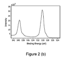
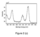
- the substrate was then dried and the presence of an approximately 100 nanometer (nm) GST film was confirmed by SEM ( Figure 1 ) and XPS ( Figure 2(a)-(c) ).
- Cadmium telluride was deposited on Si(100) substrates. Four baths were prepared respectively containing:
- the substrate was dipped in each bath for 3 seconds before being moved on to the next one in turn, and the full cycle was repeated 100 times. The substrate was then dried.
Landscapes
- Chemical & Material Sciences (AREA)
- Engineering & Computer Science (AREA)
- Organic Chemistry (AREA)
- General Chemical & Material Sciences (AREA)
- Chemical Kinetics & Catalysis (AREA)
- Materials Engineering (AREA)
- Mechanical Engineering (AREA)
- Metallurgy (AREA)
- Thermal Sciences (AREA)
- Physics & Mathematics (AREA)
- Inorganic Chemistry (AREA)
- Manufacturing & Machinery (AREA)
- Chemical Vapour Deposition (AREA)
- Semiconductor Memories (AREA)
- Chemically Coating (AREA)
- Other Surface Treatments For Metallic Materials (AREA)
- Liquid Deposition Of Substances Of Which Semiconductor Devices Are Composed (AREA)
- Photovoltaic Devices (AREA)
- Application Of Or Painting With Fluid Materials (AREA)
- Laminated Bodies (AREA)
Applications Claiming Priority (2)
| Application Number | Priority Date | Filing Date | Title |
|---|---|---|---|
| US30722210P | 2010-02-23 | 2010-02-23 | |
| US13/023,145 US8193027B2 (en) | 2010-02-23 | 2011-02-08 | Method of making a multicomponent film |
Publications (3)
| Publication Number | Publication Date |
|---|---|
| EP2394748A2 true EP2394748A2 (de) | 2011-12-14 |
| EP2394748A3 EP2394748A3 (de) | 2012-07-25 |
| EP2394748B1 EP2394748B1 (de) | 2017-03-29 |
Family
ID=44464712
Family Applications (1)
| Application Number | Title | Priority Date | Filing Date |
|---|---|---|---|
| EP11155620.5A Not-in-force EP2394748B1 (de) | 2010-02-23 | 2011-02-23 | Verfahren zur Herstellung eines Mehrkomponentenfilms |
Country Status (6)
| Country | Link |
|---|---|
| US (3) | US8193027B2 (de) |
| EP (1) | EP2394748B1 (de) |
| JP (2) | JP5727256B2 (de) |
| KR (3) | KR101266133B1 (de) |
| CN (1) | CN102163555B (de) |
| TW (1) | TWI431154B (de) |
Families Citing this family (25)
| Publication number | Priority date | Publication date | Assignee | Title |
|---|---|---|---|---|
| US8765223B2 (en) * | 2008-05-08 | 2014-07-01 | Air Products And Chemicals, Inc. | Binary and ternary metal chalcogenide materials and method of making and using same |
| KR20140021979A (ko) * | 2012-08-13 | 2014-02-21 | 에어 프로덕츠 앤드 케미칼스, 인코오포레이티드 | Ald/cvd 공정에서 gst 필름을 위한 전구체 |
| TWI485872B (zh) * | 2012-11-05 | 2015-05-21 | Ind Tech Res Inst | 漿料與太陽能電池之吸光層的形成方法 |
| US9214630B2 (en) | 2013-04-11 | 2015-12-15 | Air Products And Chemicals, Inc. | Method of making a multicomponent film |
| US10253414B2 (en) * | 2014-09-30 | 2019-04-09 | Tokyo Electron Limited | Liquid phase atomic layer deposition |
| US10020185B2 (en) | 2014-10-07 | 2018-07-10 | Samsung Sdi Co., Ltd. | Composition for forming silica layer, silica layer, and electronic device |
| US20160172188A1 (en) * | 2014-12-16 | 2016-06-16 | Samsung Sdi Co., Ltd. | Rinse solution for silica thin film, method of producing silica thin film, and silica thin film |
| KR101837971B1 (ko) | 2014-12-19 | 2018-03-13 | 삼성에스디아이 주식회사 | 실리카계 막 형성용 조성물, 실리카계 막, 및 전자 디바이스 |
| KR101833800B1 (ko) | 2014-12-19 | 2018-03-02 | 삼성에스디아이 주식회사 | 실리카계 막 형성용 조성물, 실리카계 막의 제조방법 및 상기 실리카계 막을 포함하는 전자 소자 |
| KR20170014946A (ko) | 2015-07-31 | 2017-02-08 | 삼성에스디아이 주식회사 | 실리카 막 형성용 조성물, 실리카 막의 제조방법 및 실리카 막 |
| US10062568B2 (en) * | 2016-05-13 | 2018-08-28 | Nanoco Technologies, Ltd. | Chemical vapor deposition method for fabricating two-dimensional materials |
| US10889887B2 (en) | 2016-08-22 | 2021-01-12 | Honeywell International Inc. | Chalcogenide sputtering target and method of making the same |
| KR101810892B1 (ko) * | 2016-09-13 | 2017-12-20 | 동우 화인켐 주식회사 | 터치 센서 및 이를 포함하는 터치 스크린 패널 |
| TW201823501A (zh) * | 2016-11-16 | 2018-07-01 | 美商陶氏全球科技有限責任公司 | 用於製造膜上之薄塗層之方法 |
| US11990609B2 (en) | 2017-06-20 | 2024-05-21 | Coreshell Technologies, Incorporated | Solution-deposited electrode coatings for thermal runaway mitigation in rechargeable batteries |
| JP7200143B2 (ja) | 2017-06-20 | 2023-01-06 | コアシェル テクノロジーズ インコーポレイテッド | バッテリー電極の表面上に薄膜の液相堆積を行うための方法、システム、及び組成物 |
| US11961991B2 (en) | 2017-06-20 | 2024-04-16 | Coreshell Technologies, Incorporated | Solution-phase deposition of thin films on solid-state electrolytes |
| US11149356B2 (en) | 2017-12-19 | 2021-10-19 | Battelle Energy Alliance, Llc | Methods of forming metals using ionic liquids |
| SG11202101337SA (en) * | 2018-09-06 | 2021-03-30 | Nat Univ Singapore | A continuous thin film of a metal chalcogenide |
| US11121319B2 (en) | 2019-12-11 | 2021-09-14 | International Business Machines Corporation | Phase-change memory with no drift |
| US11482506B2 (en) | 2020-03-31 | 2022-10-25 | Taiwan Semiconductor Manufacturing Company Limited | Edge-trimming methods for wafer bonding and dicing |
| CN114319071B (zh) * | 2022-02-25 | 2024-06-21 | 鸿海精密工业股份有限公司 | 浮桥结构及红外线感测装置 |
| KR102718960B1 (ko) * | 2023-01-31 | 2024-10-18 | 한국화학연구원 | 안티모니 칼코게나이드를 제조하는 방법 |
| CN116768627B (zh) * | 2023-06-21 | 2024-04-12 | 深圳大学 | 一种碲化锗基热电材料及其制备方法 |
| US20250320600A1 (en) * | 2024-04-12 | 2025-10-16 | Micron Technology, Inc. | Forming an indium chalcogenide film |
Family Cites Families (17)
| Publication number | Priority date | Publication date | Assignee | Title |
|---|---|---|---|---|
| JPS61110773A (ja) * | 1984-11-05 | 1986-05-29 | Hitachi Ltd | 薄膜の製造方法 |
| US6204402B1 (en) * | 1998-12-22 | 2001-03-20 | Advanced Technology Materials, Inc. | Indium source reagent compositions, and use thereof for deposition of indium-containing films on substrates and ion implantation of indium-doped shallow junction microelectronics structures |
| US6689700B1 (en) * | 1999-11-02 | 2004-02-10 | University Of Massachusetts | Chemical fluid deposition method for the formation of metal and metal alloy films on patterned and unpatterned substrates |
| US6527866B1 (en) * | 2000-02-09 | 2003-03-04 | Conductus, Inc. | Apparatus and method for deposition of thin films |
| US6984591B1 (en) * | 2000-04-20 | 2006-01-10 | International Business Machines Corporation | Precursor source mixtures |
| US8354046B2 (en) * | 2004-07-08 | 2013-01-15 | Los Alamos National Security, Llc | Germanium films by polymer-assisted deposition |
| CN100490205C (zh) * | 2003-07-10 | 2009-05-20 | 国际商业机器公司 | 淀积金属硫族化物膜的方法和制备场效应晶体管的方法 |
| TWI299527B (en) | 2006-04-11 | 2008-08-01 | Taiwan Tft Lcd Ass | A fabrication method of thin film for active layer by metal chalcogenide precursor solution |
| US7854963B2 (en) * | 2006-10-13 | 2010-12-21 | Solopower, Inc. | Method and apparatus for controlling composition profile of copper indium gallium chalcogenide layers |
| US7820474B2 (en) | 2007-01-09 | 2010-10-26 | International Business Machines Corporation | Metal catalyzed selective deposition of materials including germanium and antimony |
| US8377341B2 (en) * | 2007-04-24 | 2013-02-19 | Air Products And Chemicals, Inc. | Tellurium (Te) precursors for making phase change memory materials |
| US8454928B2 (en) | 2007-09-17 | 2013-06-04 | L'air Liquide Societe Anonyme Pour L'etude Et L'exploitation Des Procedes Georges Claude | Tellurium precursors for GST deposition |
| US7704895B2 (en) | 2008-04-02 | 2010-04-27 | Intel Corporation | Deposition method for high-k dielectric materials |
| KR101515544B1 (ko) * | 2008-04-18 | 2015-04-30 | 주식회사 원익아이피에스 | 칼코제나이드 박막 형성방법 |
| KR101580575B1 (ko) * | 2008-04-25 | 2015-12-28 | 에이에스엠 인터내셔널 엔.브이. | 텔루르와 셀렌 박막의 원자층 증착을 위한 전구체의 합성과 그 용도 |
| US8765223B2 (en) * | 2008-05-08 | 2014-07-01 | Air Products And Chemicals, Inc. | Binary and ternary metal chalcogenide materials and method of making and using same |
| WO2010120702A1 (en) * | 2009-04-14 | 2010-10-21 | Reel Solar Incorporated | Apparatus and methods for chemical electrodeposition on a substrate for solar cell fabrication |
-
2011
- 2011-02-08 US US13/023,145 patent/US8193027B2/en not_active Expired - Fee Related
- 2011-02-21 TW TW100105688A patent/TWI431154B/zh not_active IP Right Cessation
- 2011-02-22 JP JP2011035639A patent/JP5727256B2/ja not_active Expired - Fee Related
- 2011-02-23 CN CN201110048467.XA patent/CN102163555B/zh not_active Expired - Fee Related
- 2011-02-23 EP EP11155620.5A patent/EP2394748B1/de not_active Not-in-force
- 2011-02-23 KR KR1020110016047A patent/KR101266133B1/ko not_active Expired - Fee Related
-
2012
- 2012-05-08 US US13/466,275 patent/US8563353B2/en not_active Expired - Fee Related
-
2013
- 2013-02-07 KR KR1020130013937A patent/KR101652451B1/ko not_active Expired - Fee Related
- 2013-09-20 US US14/032,985 patent/US20140024173A1/en not_active Abandoned
-
2014
- 2014-09-11 JP JP2014185486A patent/JP2015038246A/ja not_active Withdrawn
-
2016
- 2016-07-07 KR KR1020160086119A patent/KR20160086303A/ko not_active Ceased
Non-Patent Citations (1)
| Title |
|---|
| None |
Also Published As
| Publication number | Publication date |
|---|---|
| KR101266133B1 (ko) | 2013-05-27 |
| KR20160086303A (ko) | 2016-07-19 |
| JP5727256B2 (ja) | 2015-06-03 |
| JP2015038246A (ja) | 2015-02-26 |
| JP2012082507A (ja) | 2012-04-26 |
| US8193027B2 (en) | 2012-06-05 |
| EP2394748A3 (de) | 2012-07-25 |
| KR20130026467A (ko) | 2013-03-13 |
| TWI431154B (zh) | 2014-03-21 |
| US20120034767A1 (en) | 2012-02-09 |
| US20120220076A1 (en) | 2012-08-30 |
| US20140024173A1 (en) | 2014-01-23 |
| CN102163555A (zh) | 2011-08-24 |
| EP2394748B1 (de) | 2017-03-29 |
| KR101652451B1 (ko) | 2016-09-09 |
| US8563353B2 (en) | 2013-10-22 |
| CN102163555B (zh) | 2014-07-02 |
| TW201131014A (en) | 2011-09-16 |
| KR20110097692A (ko) | 2011-08-31 |
Similar Documents
| Publication | Publication Date | Title |
|---|---|---|
| US8563353B2 (en) | Method of making a multicomponent film | |
| TWI394859B (zh) | 二元及三元金屬硫族化合物材料及其製造與使用方法 | |
| TWI452167B (zh) | 二元及三元金屬硫族化合物材料及其製造與使用方法 | |
| US8507040B2 (en) | Binary and ternary metal chalcogenide materials and method of making and using same | |
| KR101634742B1 (ko) | 다성분 필름을 제조하는 방법 |
Legal Events
| Date | Code | Title | Description |
|---|---|---|---|
| AK | Designated contracting states |
Kind code of ref document: A2 Designated state(s): AL AT BE BG CH CY CZ DE DK EE ES FI FR GB GR HR HU IE IS IT LI LT LU LV MC MK MT NL NO PL PT RO RS SE SI SK SM TR |
|
| AX | Request for extension of the european patent |
Extension state: BA ME |
|
| PUAI | Public reference made under article 153(3) epc to a published international application that has entered the european phase |
Free format text: ORIGINAL CODE: 0009012 |
|
| PUAL | Search report despatched |
Free format text: ORIGINAL CODE: 0009013 |
|
| AK | Designated contracting states |
Kind code of ref document: A3 Designated state(s): AL AT BE BG CH CY CZ DE DK EE ES FI FR GB GR HR HU IE IS IT LI LT LU LV MC MK MT NL NO PL PT RO RS SE SI SK SM TR |
|
| AX | Request for extension of the european patent |
Extension state: BA ME |
|
| RIC1 | Information provided on ipc code assigned before grant |
Ipc: C23C 18/12 20060101ALI20120618BHEP Ipc: B05D 1/36 20060101AFI20120618BHEP |
|
| 17P | Request for examination filed |
Effective date: 20130125 |
|
| 17Q | First examination report despatched |
Effective date: 20130322 |
|
| GRAP | Despatch of communication of intention to grant a patent |
Free format text: ORIGINAL CODE: EPIDOSNIGR1 |
|
| INTG | Intention to grant announced |
Effective date: 20161017 |
|
| GRAS | Grant fee paid |
Free format text: ORIGINAL CODE: EPIDOSNIGR3 |
|
| GRAA | (expected) grant |
Free format text: ORIGINAL CODE: 0009210 |
|
| AK | Designated contracting states |
Kind code of ref document: B1 Designated state(s): AL AT BE BG CH CY CZ DE DK EE ES FI FR GB GR HR HU IE IS IT LI LT LU LV MC MK MT NL NO PL PT RO RS SE SI SK SM TR |
|
| REG | Reference to a national code |
Ref country code: GB Ref legal event code: FG4D |
|
| REG | Reference to a national code |
Ref country code: CH Ref legal event code: EP |
|
| REG | Reference to a national code |
Ref country code: AT Ref legal event code: REF Ref document number: 879240 Country of ref document: AT Kind code of ref document: T Effective date: 20170415 |
|
| REG | Reference to a national code |
Ref country code: IE Ref legal event code: FG4D |
|
| REG | Reference to a national code |
Ref country code: DE Ref legal event code: R096 Ref document number: 602011036374 Country of ref document: DE |
|
| PG25 | Lapsed in a contracting state [announced via postgrant information from national office to epo] |
Ref country code: GR Free format text: LAPSE BECAUSE OF FAILURE TO SUBMIT A TRANSLATION OF THE DESCRIPTION OR TO PAY THE FEE WITHIN THE PRESCRIBED TIME-LIMIT Effective date: 20170630 Ref country code: FI Free format text: LAPSE BECAUSE OF FAILURE TO SUBMIT A TRANSLATION OF THE DESCRIPTION OR TO PAY THE FEE WITHIN THE PRESCRIBED TIME-LIMIT Effective date: 20170329 Ref country code: HR Free format text: LAPSE BECAUSE OF FAILURE TO SUBMIT A TRANSLATION OF THE DESCRIPTION OR TO PAY THE FEE WITHIN THE PRESCRIBED TIME-LIMIT Effective date: 20170329 Ref country code: LT Free format text: LAPSE BECAUSE OF FAILURE TO SUBMIT A TRANSLATION OF THE DESCRIPTION OR TO PAY THE FEE WITHIN THE PRESCRIBED TIME-LIMIT Effective date: 20170329 Ref country code: NO Free format text: LAPSE BECAUSE OF FAILURE TO SUBMIT A TRANSLATION OF THE DESCRIPTION OR TO PAY THE FEE WITHIN THE PRESCRIBED TIME-LIMIT Effective date: 20170629 |
|
| REG | Reference to a national code |
Ref country code: NL Ref legal event code: MP Effective date: 20170329 |
|
| REG | Reference to a national code |
Ref country code: AT Ref legal event code: MK05 Ref document number: 879240 Country of ref document: AT Kind code of ref document: T Effective date: 20170329 |
|
| PG25 | Lapsed in a contracting state [announced via postgrant information from national office to epo] |
Ref country code: LV Free format text: LAPSE BECAUSE OF FAILURE TO SUBMIT A TRANSLATION OF THE DESCRIPTION OR TO PAY THE FEE WITHIN THE PRESCRIBED TIME-LIMIT Effective date: 20170329 Ref country code: SE Free format text: LAPSE BECAUSE OF FAILURE TO SUBMIT A TRANSLATION OF THE DESCRIPTION OR TO PAY THE FEE WITHIN THE PRESCRIBED TIME-LIMIT Effective date: 20170329 Ref country code: BG Free format text: LAPSE BECAUSE OF FAILURE TO SUBMIT A TRANSLATION OF THE DESCRIPTION OR TO PAY THE FEE WITHIN THE PRESCRIBED TIME-LIMIT Effective date: 20170629 Ref country code: RS Free format text: LAPSE BECAUSE OF FAILURE TO SUBMIT A TRANSLATION OF THE DESCRIPTION OR TO PAY THE FEE WITHIN THE PRESCRIBED TIME-LIMIT Effective date: 20170329 |
|
| RAP2 | Party data changed (patent owner data changed or rights of a patent transferred) |
Owner name: VERSUM MATERIALS US, LLC |
|
| PG25 | Lapsed in a contracting state [announced via postgrant information from national office to epo] |
Ref country code: NL Free format text: LAPSE BECAUSE OF FAILURE TO SUBMIT A TRANSLATION OF THE DESCRIPTION OR TO PAY THE FEE WITHIN THE PRESCRIBED TIME-LIMIT Effective date: 20170329 |
|
| PG25 | Lapsed in a contracting state [announced via postgrant information from national office to epo] |
Ref country code: AT Free format text: LAPSE BECAUSE OF FAILURE TO SUBMIT A TRANSLATION OF THE DESCRIPTION OR TO PAY THE FEE WITHIN THE PRESCRIBED TIME-LIMIT Effective date: 20170329 Ref country code: ES Free format text: LAPSE BECAUSE OF FAILURE TO SUBMIT A TRANSLATION OF THE DESCRIPTION OR TO PAY THE FEE WITHIN THE PRESCRIBED TIME-LIMIT Effective date: 20170329 Ref country code: SK Free format text: LAPSE BECAUSE OF FAILURE TO SUBMIT A TRANSLATION OF THE DESCRIPTION OR TO PAY THE FEE WITHIN THE PRESCRIBED TIME-LIMIT Effective date: 20170329 Ref country code: EE Free format text: LAPSE BECAUSE OF FAILURE TO SUBMIT A TRANSLATION OF THE DESCRIPTION OR TO PAY THE FEE WITHIN THE PRESCRIBED TIME-LIMIT Effective date: 20170329 Ref country code: CZ Free format text: LAPSE BECAUSE OF FAILURE TO SUBMIT A TRANSLATION OF THE DESCRIPTION OR TO PAY THE FEE WITHIN THE PRESCRIBED TIME-LIMIT Effective date: 20170329 Ref country code: RO Free format text: LAPSE BECAUSE OF FAILURE TO SUBMIT A TRANSLATION OF THE DESCRIPTION OR TO PAY THE FEE WITHIN THE PRESCRIBED TIME-LIMIT Effective date: 20170329 |
|
| REG | Reference to a national code |
Ref country code: DE Ref legal event code: R082 Ref document number: 602011036374 Country of ref document: DE Representative=s name: KADOR & PARTNER PART MBB PATENTANWAELTE, DE Ref country code: DE Ref legal event code: R081 Ref document number: 602011036374 Country of ref document: DE Owner name: VERSUM MATERIALS US, LLC, TEMPE, US Free format text: FORMER OWNER: AIR PRODUCTS AND CHEMICALS, INC., ALLENTOWN, PA., US Ref country code: DE Ref legal event code: R082 Ref document number: 602011036374 Country of ref document: DE Representative=s name: KADOR & PARTNER PARTG MBB PATENTANWAELTE, DE |
|
| PG25 | Lapsed in a contracting state [announced via postgrant information from national office to epo] |
Ref country code: PL Free format text: LAPSE BECAUSE OF FAILURE TO SUBMIT A TRANSLATION OF THE DESCRIPTION OR TO PAY THE FEE WITHIN THE PRESCRIBED TIME-LIMIT Effective date: 20170329 Ref country code: PT Free format text: LAPSE BECAUSE OF FAILURE TO SUBMIT A TRANSLATION OF THE DESCRIPTION OR TO PAY THE FEE WITHIN THE PRESCRIBED TIME-LIMIT Effective date: 20170731 Ref country code: IS Free format text: LAPSE BECAUSE OF FAILURE TO SUBMIT A TRANSLATION OF THE DESCRIPTION OR TO PAY THE FEE WITHIN THE PRESCRIBED TIME-LIMIT Effective date: 20170729 Ref country code: SM Free format text: LAPSE BECAUSE OF FAILURE TO SUBMIT A TRANSLATION OF THE DESCRIPTION OR TO PAY THE FEE WITHIN THE PRESCRIBED TIME-LIMIT Effective date: 20170329 |
|
| REG | Reference to a national code |
Ref country code: DE Ref legal event code: R097 Ref document number: 602011036374 Country of ref document: DE |
|
| REG | Reference to a national code |
Ref country code: FR Ref legal event code: PLFP Year of fee payment: 8 |
|
| PG25 | Lapsed in a contracting state [announced via postgrant information from national office to epo] |
Ref country code: DK Free format text: LAPSE BECAUSE OF FAILURE TO SUBMIT A TRANSLATION OF THE DESCRIPTION OR TO PAY THE FEE WITHIN THE PRESCRIBED TIME-LIMIT Effective date: 20170329 |
|
| PLBE | No opposition filed within time limit |
Free format text: ORIGINAL CODE: 0009261 |
|
| STAA | Information on the status of an ep patent application or granted ep patent |
Free format text: STATUS: NO OPPOSITION FILED WITHIN TIME LIMIT |
|
| PG25 | Lapsed in a contracting state [announced via postgrant information from national office to epo] |
Ref country code: IT Free format text: LAPSE BECAUSE OF FAILURE TO SUBMIT A TRANSLATION OF THE DESCRIPTION OR TO PAY THE FEE WITHIN THE PRESCRIBED TIME-LIMIT Effective date: 20170329 |
|
| 26N | No opposition filed |
Effective date: 20180103 |
|
| PG25 | Lapsed in a contracting state [announced via postgrant information from national office to epo] |
Ref country code: SI Free format text: LAPSE BECAUSE OF FAILURE TO SUBMIT A TRANSLATION OF THE DESCRIPTION OR TO PAY THE FEE WITHIN THE PRESCRIBED TIME-LIMIT Effective date: 20170329 |
|
| REG | Reference to a national code |
Ref country code: FR Ref legal event code: TP Owner name: VERSUM MATERIALS US, LLC, US Effective date: 20180711 |
|
| REG | Reference to a national code |
Ref country code: CH Ref legal event code: PL |
|
| PG25 | Lapsed in a contracting state [announced via postgrant information from national office to epo] |
Ref country code: MC Free format text: LAPSE BECAUSE OF FAILURE TO SUBMIT A TRANSLATION OF THE DESCRIPTION OR TO PAY THE FEE WITHIN THE PRESCRIBED TIME-LIMIT Effective date: 20170329 |
|
| GBPC | Gb: european patent ceased through non-payment of renewal fee |
Effective date: 20180223 |
|
| REG | Reference to a national code |
Ref country code: IE Ref legal event code: MM4A |
|
| REG | Reference to a national code |
Ref country code: BE Ref legal event code: MM Effective date: 20180228 |
|
| PG25 | Lapsed in a contracting state [announced via postgrant information from national office to epo] |
Ref country code: LU Free format text: LAPSE BECAUSE OF NON-PAYMENT OF DUE FEES Effective date: 20180223 Ref country code: CH Free format text: LAPSE BECAUSE OF NON-PAYMENT OF DUE FEES Effective date: 20180228 Ref country code: LI Free format text: LAPSE BECAUSE OF NON-PAYMENT OF DUE FEES Effective date: 20180228 |
|
| PG25 | Lapsed in a contracting state [announced via postgrant information from national office to epo] |
Ref country code: IE Free format text: LAPSE BECAUSE OF NON-PAYMENT OF DUE FEES Effective date: 20180223 |
|
| PG25 | Lapsed in a contracting state [announced via postgrant information from national office to epo] |
Ref country code: GB Free format text: LAPSE BECAUSE OF NON-PAYMENT OF DUE FEES Effective date: 20180223 Ref country code: BE Free format text: LAPSE BECAUSE OF NON-PAYMENT OF DUE FEES Effective date: 20180228 |
|
| PG25 | Lapsed in a contracting state [announced via postgrant information from national office to epo] |
Ref country code: MT Free format text: LAPSE BECAUSE OF NON-PAYMENT OF DUE FEES Effective date: 20180223 |
|
| PG25 | Lapsed in a contracting state [announced via postgrant information from national office to epo] |
Ref country code: TR Free format text: LAPSE BECAUSE OF FAILURE TO SUBMIT A TRANSLATION OF THE DESCRIPTION OR TO PAY THE FEE WITHIN THE PRESCRIBED TIME-LIMIT Effective date: 20170329 |
|
| PG25 | Lapsed in a contracting state [announced via postgrant information from national office to epo] |
Ref country code: HU Free format text: LAPSE BECAUSE OF FAILURE TO SUBMIT A TRANSLATION OF THE DESCRIPTION OR TO PAY THE FEE WITHIN THE PRESCRIBED TIME-LIMIT; INVALID AB INITIO Effective date: 20110223 |
|
| PG25 | Lapsed in a contracting state [announced via postgrant information from national office to epo] |
Ref country code: CY Free format text: LAPSE BECAUSE OF FAILURE TO SUBMIT A TRANSLATION OF THE DESCRIPTION OR TO PAY THE FEE WITHIN THE PRESCRIBED TIME-LIMIT Effective date: 20170329 Ref country code: MK Free format text: LAPSE BECAUSE OF NON-PAYMENT OF DUE FEES Effective date: 20170329 |
|
| PG25 | Lapsed in a contracting state [announced via postgrant information from national office to epo] |
Ref country code: AL Free format text: LAPSE BECAUSE OF FAILURE TO SUBMIT A TRANSLATION OF THE DESCRIPTION OR TO PAY THE FEE WITHIN THE PRESCRIBED TIME-LIMIT Effective date: 20170329 |
|
| PGFP | Annual fee paid to national office [announced via postgrant information from national office to epo] |
Ref country code: FR Payment date: 20210113 Year of fee payment: 11 |
|
| PGFP | Annual fee paid to national office [announced via postgrant information from national office to epo] |
Ref country code: DE Payment date: 20210209 Year of fee payment: 11 |
|
| REG | Reference to a national code |
Ref country code: DE Ref legal event code: R119 Ref document number: 602011036374 Country of ref document: DE |
|
| PG25 | Lapsed in a contracting state [announced via postgrant information from national office to epo] |
Ref country code: FR Free format text: LAPSE BECAUSE OF NON-PAYMENT OF DUE FEES Effective date: 20220228 |
|
| PG25 | Lapsed in a contracting state [announced via postgrant information from national office to epo] |
Ref country code: DE Free format text: LAPSE BECAUSE OF NON-PAYMENT OF DUE FEES Effective date: 20220901 |
|
| P01 | Opt-out of the competence of the unified patent court (upc) registered |
Effective date: 20230602 |