EP2392252A1 - Endoscope system with interlaced image transmission - Google Patents
Endoscope system with interlaced image transmission Download PDFInfo
- Publication number
- EP2392252A1 EP2392252A1 EP11168803A EP11168803A EP2392252A1 EP 2392252 A1 EP2392252 A1 EP 2392252A1 EP 11168803 A EP11168803 A EP 11168803A EP 11168803 A EP11168803 A EP 11168803A EP 2392252 A1 EP2392252 A1 EP 2392252A1
- Authority
- EP
- European Patent Office
- Prior art keywords
- lines
- line
- endoscope
- signal
- scanning mode
- Prior art date
- Legal status (The legal status is an assumption and is not a legal conclusion. Google has not performed a legal analysis and makes no representation as to the accuracy of the status listed.)
- Granted
Links
Images


Classifications
-
- H—ELECTRICITY
- H04—ELECTRIC COMMUNICATION TECHNIQUE
- H04L—TRANSMISSION OF DIGITAL INFORMATION, e.g. TELEGRAPHIC COMMUNICATION
- H04L25/00—Baseband systems
- H04L25/38—Synchronous or start-stop systems, e.g. for Baudot code
- H04L25/40—Transmitting circuits; Receiving circuits
- H04L25/49—Transmitting circuits; Receiving circuits using code conversion at the transmitter; using predistortion; using insertion of idle bits for obtaining a desired frequency spectrum; using three or more amplitude levels ; Baseband coding techniques specific to data transmission systems
- H04L25/4906—Transmitting circuits; Receiving circuits using code conversion at the transmitter; using predistortion; using insertion of idle bits for obtaining a desired frequency spectrum; using three or more amplitude levels ; Baseband coding techniques specific to data transmission systems using binary codes
- H04L25/4908—Transmitting circuits; Receiving circuits using code conversion at the transmitter; using predistortion; using insertion of idle bits for obtaining a desired frequency spectrum; using three or more amplitude levels ; Baseband coding techniques specific to data transmission systems using binary codes using mBnB codes
-
- A—HUMAN NECESSITIES
- A61—MEDICAL OR VETERINARY SCIENCE; HYGIENE
- A61B—DIAGNOSIS; SURGERY; IDENTIFICATION
- A61B1/00—Instruments for performing medical examinations of the interior of cavities or tubes of the body by visual or photographical inspection, e.g. endoscopes; Illuminating arrangements therefor
- A61B1/00002—Operational features of endoscopes
- A61B1/00004—Operational features of endoscopes characterised by electronic signal processing
- A61B1/00009—Operational features of endoscopes characterised by electronic signal processing of image signals during a use of endoscope
- A61B1/000095—Operational features of endoscopes characterised by electronic signal processing of image signals during a use of endoscope for image enhancement
-
- A—HUMAN NECESSITIES
- A61—MEDICAL OR VETERINARY SCIENCE; HYGIENE
- A61B—DIAGNOSIS; SURGERY; IDENTIFICATION
- A61B1/00—Instruments for performing medical examinations of the interior of cavities or tubes of the body by visual or photographical inspection, e.g. endoscopes; Illuminating arrangements therefor
- A61B1/04—Instruments for performing medical examinations of the interior of cavities or tubes of the body by visual or photographical inspection, e.g. endoscopes; Illuminating arrangements therefor combined with photographic or television appliances
- A61B1/05—Instruments for performing medical examinations of the interior of cavities or tubes of the body by visual or photographical inspection, e.g. endoscopes; Illuminating arrangements therefor combined with photographic or television appliances characterised by the image sensor, e.g. camera, being in the distal end portion
-
- H—ELECTRICITY
- H04—ELECTRIC COMMUNICATION TECHNIQUE
- H04N—PICTORIAL COMMUNICATION, e.g. TELEVISION
- H04N23/00—Cameras or camera modules comprising electronic image sensors; Control thereof
- H04N23/50—Constructional details
- H04N23/555—Constructional details for picking-up images in sites, inaccessible due to their dimensions or hazardous conditions, e.g. endoscopes or borescopes
-
- H—ELECTRICITY
- H04—ELECTRIC COMMUNICATION TECHNIQUE
- H04N—PICTORIAL COMMUNICATION, e.g. TELEVISION
- H04N25/00—Circuitry of solid-state image sensors [SSIS]; Control thereof
- H04N25/40—Extracting pixel data from image sensors by controlling scanning circuits, e.g. by modifying the number of pixels sampled or to be sampled
- H04N25/42—Extracting pixel data from image sensors by controlling scanning circuits, e.g. by modifying the number of pixels sampled or to be sampled by switching between different modes of operation using different resolutions or aspect ratios, e.g. switching between interlaced and non-interlaced mode
-
- H—ELECTRICITY
- H04—ELECTRIC COMMUNICATION TECHNIQUE
- H04N—PICTORIAL COMMUNICATION, e.g. TELEVISION
- H04N25/00—Circuitry of solid-state image sensors [SSIS]; Control thereof
- H04N25/50—Control of the SSIS exposure
- H04N25/53—Control of the integration time
- H04N25/531—Control of the integration time by controlling rolling shutters in CMOS SSIS
-
- A—HUMAN NECESSITIES
- A61—MEDICAL OR VETERINARY SCIENCE; HYGIENE
- A61B—DIAGNOSIS; SURGERY; IDENTIFICATION
- A61B1/00—Instruments for performing medical examinations of the interior of cavities or tubes of the body by visual or photographical inspection, e.g. endoscopes; Illuminating arrangements therefor
- A61B1/00002—Operational features of endoscopes
- A61B1/00011—Operational features of endoscopes characterised by signal transmission
- A61B1/00018—Operational features of endoscopes characterised by signal transmission using electrical cables
-
- A—HUMAN NECESSITIES
- A61—MEDICAL OR VETERINARY SCIENCE; HYGIENE
- A61B—DIAGNOSIS; SURGERY; IDENTIFICATION
- A61B1/00—Instruments for performing medical examinations of the interior of cavities or tubes of the body by visual or photographical inspection, e.g. endoscopes; Illuminating arrangements therefor
- A61B1/00002—Operational features of endoscopes
- A61B1/00043—Operational features of endoscopes provided with output arrangements
- A61B1/00045—Display arrangement
-
- A—HUMAN NECESSITIES
- A61—MEDICAL OR VETERINARY SCIENCE; HYGIENE
- A61B—DIAGNOSIS; SURGERY; IDENTIFICATION
- A61B1/00—Instruments for performing medical examinations of the interior of cavities or tubes of the body by visual or photographical inspection, e.g. endoscopes; Illuminating arrangements therefor
- A61B1/005—Flexible endoscopes
- A61B1/0051—Flexible endoscopes with controlled bending of insertion part
- A61B1/0052—Constructional details of control elements, e.g. handles
-
- A—HUMAN NECESSITIES
- A61—MEDICAL OR VETERINARY SCIENCE; HYGIENE
- A61B—DIAGNOSIS; SURGERY; IDENTIFICATION
- A61B1/00—Instruments for performing medical examinations of the interior of cavities or tubes of the body by visual or photographical inspection, e.g. endoscopes; Illuminating arrangements therefor
- A61B1/012—Instruments for performing medical examinations of the interior of cavities or tubes of the body by visual or photographical inspection, e.g. endoscopes; Illuminating arrangements therefor characterised by internal passages or accessories therefor
- A61B1/018—Instruments for performing medical examinations of the interior of cavities or tubes of the body by visual or photographical inspection, e.g. endoscopes; Illuminating arrangements therefor characterised by internal passages or accessories therefor for receiving instruments
-
- A—HUMAN NECESSITIES
- A61—MEDICAL OR VETERINARY SCIENCE; HYGIENE
- A61B—DIAGNOSIS; SURGERY; IDENTIFICATION
- A61B18/00—Surgical instruments, devices or methods for transferring non-mechanical forms of energy to or from the body
- A61B18/04—Surgical instruments, devices or methods for transferring non-mechanical forms of energy to or from the body by heating
- A61B18/12—Surgical instruments, devices or methods for transferring non-mechanical forms of energy to or from the body by heating by passing a current through the tissue to be heated, e.g. high-frequency current
- A61B18/14—Probes or electrodes therefor
- A61B18/1492—Probes or electrodes therefor having a flexible, catheter-like structure, e.g. for heart ablation
-
- A—HUMAN NECESSITIES
- A61—MEDICAL OR VETERINARY SCIENCE; HYGIENE
- A61B—DIAGNOSIS; SURGERY; IDENTIFICATION
- A61B18/00—Surgical instruments, devices or methods for transferring non-mechanical forms of energy to or from the body
- A61B18/04—Surgical instruments, devices or methods for transferring non-mechanical forms of energy to or from the body by heating
- A61B18/12—Surgical instruments, devices or methods for transferring non-mechanical forms of energy to or from the body by heating by passing a current through the tissue to be heated, e.g. high-frequency current
- A61B18/14—Probes or electrodes therefor
- A61B2018/1475—Electrodes retractable in or deployable from a housing
Definitions
- the present invention relates to an endoscope system.
- JP-A-60-55923 As a technology for signal transmission of a captured image between an endoscope and a controller connected to the endoscope, a system employing analog transmission is described in JP-A-60-55923 .
- a noise elimination device generates positive and negative video signals on the basis of image information of a captured image and these video signals are synchronized with each other and transmitted to the controller, so that degradation in the image quality may be restored by utilizing the symmetry between these video signals.
- image information may be transmitted with high noise resistance and without causing a large failure in the image.
- An object of the invention is providing an endoscope system capable of outputting high quality image information by making influence of noise inconspicuous even if a captured image signal is externally influenced by noise during serial transmission of the captured image signal from an endoscope to a controller.
- an endoscope system includes:
- FIG. 1 is a schematic diagram illustrating the whole structure of an endoscope system including an endoscopic device for explaining the embodiment of the invention.
- the endoscope system 200 includes the endoscopic device (hereinafter sometimes referred to as the endoscope) 100, a controller 13 connected to the endoscope 100, a display section 15 such as a monitor, an input section 17 such as a keyboard, a treatment instrument 71, a high frequency power control section 97 for driving the treatment instrument 71, and a foot switch 99 connected to the high frequency power control section 97.
- the controller 13 includes a light source section 67 for supplying the endoscope 100 with illumination light and a processor section 69 for subjecting an imaging signal supplied from the endoscope 100 to various image processing for converting it into a video signal.
- the endoscope 100 includes a body operating section 21, an endoscope inserting section 23 connected to the body operating section 21 to be inserted into a body cavity, a universal cord 25 connected to the body operating section 21 and containing various duct lines and signal cables, and connectors 27A and 27B provided at the tip of the universal cord 25 to be removably connected to the controller 13.
- the connectors 27A and 27B are individual connectors to be respectively connected to the light source section 67 and the processor section 69 of the controller 13 or may be one connector of a composite type.
- the light source section 67 of the controller 13 outputs emitted light to the endoscope 100 through the connector 27A and the universal cord 25, so that illumination light may be supplied to an illuminating optical system provided at the tip of the endoscope inserting section 23.
- buttons 29 such as an air/water supply button, a suction button, a shutter button and a function switching button are arranged, and a pair of angle nobs 31 for bending a tip side of the endoscope are provided.
- the endoscope inserting section 23 includes a soft part 33, a bending part 35 and a tip part (an endoscope tip part) 37 successively disposed in this order from the side of the body operating section 21.
- the soft part 33 is flexible and is connected to the base side of the bending part 35, and the bending part 35 is capable of bending when a wire (not shown) inserted through the endoscope inserting section 23 is pulled by rotating the angle nobs 31 of the body operating section 21.
- the endoscope tip part 37 may be made to face toward a desired direction.
- FIG. 2 is an enlarged partial cross-sectional view illustrating the structure of the tip part of the endoscopic device.
- An imaging optical system provided at the tip of the endoscope inserting section 23 includes an imaging chip 51 having an imaging device 55 for capturing an image of an observed site illuminated by the illuminating optical system, and outputs an imaging signal of the observed image obtained from the imaging device 55 to the controller 13.
- As the imaging device 55 a CMOS (Complementary Metal Oxide Semiconductor) image sensor is used.
- the processor section 69 of the controller 13 displays, in the display section 15 illustrated in FIG. 1 , image information obtained through image processing of the input imaging signal.
- the input section 17 such as a keyboard connected to the controller 13 may be used for inputting commands for such a series of processing.
- the endoscope tip part 37 is provided with a lighting window (not shown) and an observation window 45 (see FIG. 2 ) as well as a clamp opening 43 of an instrument inserting hole 47.
- an objective optical system 49 including a plurality of lenses is provided for capturing an image of an observed site inside a body cavity.
- a prism 53 is connected for bending the optical axis of the objective optical system 49 at right angles to guide it toward the imaging chip 51.
- the imaging chip 51 is a monolithic semiconductor (i.e., what is called a CMOS sensor chip) integrally including the imaging device 55 and a peripheral circuit 57 for driving the imaging device 55 and for inputting/outputting signals to/from the imaging device 55, and is mounted on a substrate 59.
- a signal line 61 is connected to the rear end of the substrate 59, and the signal line 61 is connected to the processor section 69 through the universal cord 25 illustrated in FIG. 1 so as to transfer various signals.
- the objective optical system 49 and the prism 53 together form an optical image obtained on the side of the endoscope tip part 37 on the imaging device 55 of the imaging chip 51, and the imaging device 55 outputs an output signal of the optical image as a captured image signal.
- the captured image signal is transmitted from the side of the endoscope 100 to the controller 13 through the universal cord 25.
- the processor section 69 of the controller 13 subjects the captured image signal transmitted from the endoscope 100 to the image processing on the basis of a command issued from the body operating section 21 or the input part 17 of the endoscope 100, so as to generate an image for display to be supplied to the display part 15.
- a connecting part 39 disposed between the body operating section 21 and the endoscope inserting section 23 is provided with a clamp inserting section 41 through which a treatment instrument such as a clamp is inserted.
- the aforementioned treatment instrument 71 is inserted through this clamp inserting section 41 to be guided out from the tip of the endoscope tip part 37.
- the treatment instrument 71 is introduced to the endoscope tip part 37 through the instrument inserting hole 47 formed through the endoscope inserting section 23 as illustrated in FIG 2 .
- the treatment instrument 71 is a high frequency treatment instrument that may superimpose noise on a signal line adjacently provided in this embodiment, and is connected to the high frequency power control section 97 through an electric cord 95.
- the high frequency power control section 97 is connected to the controller 13 and the foot switch 99 for controlling the drive of the high frequency treatment instrument 71.
- FIG. 3 is a vertical principal part cross-sectional view illustrating the schematic structure of the high frequency treatment instrument.
- the high frequency treatment instrument 71 that is, a diathermy knife, has flexibility sufficient to be inserted into the treatment instrument inserting hole 47 of the endoscope 100 (see FIG. 2 ) and includes a sheath 75 containing a close wound coil 75a and an insulating tube 75b of tetrafluoroethylene or the like covering the close wound coil 75a, and an operation part 77 provided at the base end of the sheath 75.
- a cylindrical stopper member 79 and a ring-shaped sheath tip insulating chip 81 are provided to be covered with the insulating tube 75b.
- An operation wire 83 with a conducting property is provided inside the sheath 75 to be movable along the shaft direction, and a stopper receiving part 85 with a conducting property in contact with the stopper member 79 is attached to the tip of the operation wire 83.
- the stopper receiving part 85 is provided with and electrically connected to a high frequency electrode part 73, that is, a knife part, including a bar electrode 73 a and a plate electrode 73b.
- the operation part 77 of the high frequency treatment instrument 71 includes an operation shaft part 89 and a slider 91 slidable on the operation shaft part 89.
- the slider 91 is provided with a connector part 93 and is connected to the high frequency power control section 97 through the electric cord 95.
- the high frequency power control section 97 is connected to the switch 99 such as a foot switch.
- the base of the operation wire 83 is extended backward through an insertion hole not shown formed in the operation shaft part 89 so as to be connected to the slider 91.
- the operation wire 83 moves backward/forward along the shaft direction inside the sheath 75, so that the bar electrode 73a of the high frequency electrode part 73 may appear/disappear from the tip of the sheath 75.
- FIG. 4 is a conceptual block diagram illustrating the configuration of the endoscope system.
- the endoscope system 200 includes the endoscope 100 and the processor section 69 connected to each other through the universal cord 25.
- the imaging chip 51 including the imaging device 55 and the peripheral circuit 57 is built in the endoscope 100.
- the peripheral circuit 57 of the imaging chip 51 includes a PLL (Phase-Locked Loop) circuit 101 for generating an internal clock signal, a register 103 for setting control data in the imaging device 55, an analog/digital (A/D) converter 105 for digitalizing an imaging signal output from the imaging device 55, an 8B10B encoder 107 for subjecting the digitalized imaging signal to 8B10B type encoding, a PLL circuit 109 for generating a clock signal for serial transmission by multiplying the frequency of the internal clock signal, and a parallel/serial (P/S) converter 111 for converting the encoded imaging signal into a serial signal and outputting the serial signal.
- PLL Phase-Locked Loop
- the PLL circuit 101 is a phase locked circuit composed of a phase comparator, a loop filter, a voltage control oscillator and a frequency divider, and generates an internal clock signal ICLK in synchronization with a stable reference clock signal BCLK input from the processor section 69 and having a frequency in a prescribed proportional relationship with the frequency of the reference clock signal BCLK (i.e., having a multiplied frequency).
- the internal clock signal ICLK is supplied to respective portions of the peripheral circuit 57 and the imaging device 55.
- the register 103 holds control data CTLD input from the processor section 69 and used for driving the imaging device 55 and inputs it to the imaging device 55.
- the register 103 is a shift register for performing serial/parallel conversion, and converts the control data CTLD input in the form of a serial signal into a parallel signal to be input to the imaging device 55.
- As the control data CTLD a scanning method for pixels (such as a normal scanning or interleave scanning mode described in detail later), a pixel region to be scanned, a shutter speed (i.e., exposure time) and the like are input.
- the imaging device 55 controls a scanning circuit described later on the basis of the control data CTLD and the internal clock signal ICLK.
- the A/D converter 105 converts the imaging signal output from the imaging device 55 through quantization into an 8-bit (256-scale) digital signal and inputs the converted 8-bit digital signal to the 8B10B encoder 107 in parallel by using 8 lines.
- the 8B10B encoder 107 is an 8B10B type encoder for converting the 8-bit digital signal input from the A/D converter 105 into a 10-bit digital signal by adding redundant 2-bit data, and the conversion from 8-bit to 10-bit is conducted by using a translation table according to a standard.
- the PLL circuit 109 has a similar configuration to the PLL circuit 101, and generates the clock signal TCLK for serial transmission by multiplying the frequency of the internal clock signal ICLK by, for example, 10 and supplies the clock signal TCLK to the P/S converter 111.
- the P/S converter 111 converts the digital signal (i.e., the 10-bit parallel data) input from the 8B10B encoder 107 into 10-bit serial data in accordance with the clock signal TCLK for serial transmission generated by the PLL circuit 109.
- the frequency of the serial data resulting from the conversion is 10 times as high as the frequency of the parallel data obtained before the conversion.
- the serial data generated by the P/S converter 111 is transmitted to the processor section 69 as an imaging signal SDT through a signal line 113a running inside the universal cord 25.
- the processor section 69 includes a main control circuit (CPU) 115 for controlling the whole device, a power circuit 117 for generating a power voltage VDD and a ground voltage VSS, a reference clock generator 119 for generating the reference clock signal BCLK, a clock and data recovery (CDR) circuit 121 for receiving the imaging signal SDT from the imaging chip 51 and recovering a clock signal and a data signal from the imaging signal SDT, a PLL circuit 123 for generating a clock signal for signal processing with the same frequency as the internal clock signal ICLK used in the imaging chip 51 by multiplying the frequency of the clock signal generated by the CDR circuit 121, a serial/parallel (S/P) converter 125 for converting the data signal generated by the CDR circuit 121 into a parallel signal, an 8B10B decoder 127 for generating the imaging signal obtained before the encoding by subjecting the parallelized imaging signal to 8B10B type decoding, and an image processing circuit 129 for generating image data to be displayed in the display section 15 by
- the power circuit 117 supplies the power voltage VDD and the ground voltage VSS to the respective portions within the processor section 69 and supplies these voltages to the respective portions within the imaging chip 51 through the signal lines 113b and 113c.
- the reference clock generator 119 generates the reference clock signal BCLK with a stable frequency and inputs the reference clock signal BCLK to the PLL circuit 101 included in the imaging chip 51 through a signal line 113d.
- the CPU 115 controls the respective portions within the processor section 69, generates the aforementioned control data CTLD and inputs the control data CTLD to the register 103 included in the imaging chip 51 through a signal line 113e.
- the CDR circuit 121 detects the phase of the imaging signal SDT serially transmitted from the imaging chip 51, generates an extraction clock signal RCLK in synchronization with the frequency of the imaging signal SDT, and generates data obtained by retiming the imaging signal SDT with the extraction clock signal RCLK (i.e., retiming data or an imaging signal RSDT) by sampling the imaging signal SDT with the extraction clock signal RCLK.
- the extraction clock signal RCLK generated by the CDR circuit 121 is input to the PLL circuit 123, and the imaging signal RSDT generated by the CDR circuit 121 is input to the S/P converter 125.
- the PLL circuit 123 has a similar configuration to the aforementioned PLL circuit 101, and generates the clock signal SCLK for signal processing with the same frequency as the internal clock signal ICLK by multiplying the frequency of the extraction clock signal RCLK by 1/10.
- the PLL circuit 123 supplies the thus generated clock signal SCLK to the S/P converter 125, the 8B10B decoder 127 and the image processing circuit 129.
- the S/P converter 125 subjects the imaging signal RSDT input from the CDR circuit 121 to serial/parallel conversion, corresponding to the inverse of the parallel/serial conversion, in accordance with the clock signal SCLK generated by the PLL circuit 123, so as to generate an imaging signal of 10-bit parallel data, and inputs the imaging signal to the 8B10B decoder 127.
- the 8B10B decoder 127 conducts conversion inverse to that performed by the aforementioned 8B10B encoder 107 by using a translation table according to the 8B10B standard, and decodes the imaging signal input thereto from the 10-bit signal to the 8-bit signal.
- the 8-bit imaging signal decoded by the 8B10B decoder 127 is input to the image processing circuit 129.
- the image processing circuit 129 records the imaging signal in an internal memory on the basis of the clock signal SCLK and generates image data to be output through various image processing including white balance adjustment, gain correction, color interpolation, edge enhancement, gamma correction, color matrix calculation and the like. Furthermore, the image processing circuit 129 converts the image data into the form of a signal for displaying it in the display section 15 and outputs the signal for image display to the display section 15.
- the high frequency power control section 97 is connected to the high frequency treatment instrument 71, the CPU 115 and the switch 99, and when a foot operation of the switch 99 is conducted, a high frequency current is supplied to the high frequency treatment instrument 71 on the basis of a command issued by the CPU 115.
- the high frequency current is supplied to the high frequency electrode part 73 through the operation wire 83 disposed inside the sheath 75 of the high frequency treatment instrument 71.
- the sheath 75 In supplying the high frequency current, the sheath 75 is in a state inserted through the instrument inserting hole 47 of the endoscope 100, and therefore, noise tends to be superimposed onto the signal line 113a adjacently disposed within the endoscope inserting section 23 (see FIG. 1 ) along the instrument inserting hole 47.
- the degradation in image quality of a displayed image caused by the noise may be made inconspicuous by a method described later.
- FIG. 5 is a circuit diagram schematically illustrating the configuration of the imaging device 55.
- the imaging device 55 includes a pixel part 133 in which unit pixels 131, that is, light receiving portions, are arranged in the form of a two-dimensional matrix, a correlated double sampling (CDS) circuit 135 for performing noise suppressing processing or the like on a charge signal corresponding to an output signal from the pixel part 133, a vertical scanning circuit 137 for controlling scan of the pixel part 133 in the vertical direction and controlling a reset operation of the pixel part 133, a horizontal scanning circuit 139 for controlling scan along the horizontal direction, an output circuit 141 for outputting a charge signal having been read, and a control circuit 143 for supplying a control signal to each of the circuits 135 through 139 and controlling timing and the like of the vertical/horizontal scan and sampling.
- CDS correlated double sampling
- Each unit pixel 131 includes one photodiode D1, a transistor M1 for reset, a transistor M2 for drive (amplification) and a transistor M3 for pixel selection.
- Each unit pixel 131 is connected to a vertical scanning line (row selecting line) L1 and a horizontal scanning line (column selecting line) L2, and the unit pixels 131 are successively scanned by the vertical scanning circuit 137 and the horizontal scanning circuit 139.
- the control circuit 143 generates a control signal to be input to the vertical scanning circuit 137 and the horizontal scanning circuit 139 for scanning the rows and the columns of the pixel part 133, a control signal to be input to the vertical scanning circuit 137 for resetting charge stored in each photodiode D1, and a control signal to be input to the CDS circuit 135 for controlling connection between the pixel part 133 and the CDS circuit 135.
- the CDS circuit 135 is provided correspondingly to each column selecting line L2, so as to successively output, in accordance with a horizontal scanning signal output by the horizontal scanning circuit 139, charge signals of the respective unit pixels 131 connected to a column selecting line L1 selected by the vertical scanning circuit 137.
- the horizontal scanning circuit 139 controls, in accordance with the horizontal scanning signal, an on/off state of a transistor M4 for column selection provided between the CDS circuit 135 and an output bus line L3 connected to the output circuit 141.
- the output circuit 141 amplifies the charge signals successively sent from the CDS circuit 135 to the output bus line L3 and outputs the amplified signals.
- a signal output from the output circuit 141 is designated as an imaging signal for distinguishing it from a charge signal read from each unit pixel 131.
- the imaging device 55 is a single chip color sensor type imaging device including a color filter (such as a Bayer primary color filter) including a plurality of color segments.
- a color filter such as a Bayer primary color filter
- the pixel part 133 has a square array structure in which the unit pixels 131 are arranged in the form of a matrix along the row direction and the column direction on a semiconductor substrate, wherein the column direction is the vertical direction and the row direction is the horizontal direction.
- it may have what is called honeycomb pixel arrangement in which unit pixels 131 disposed on odd-numbered rows and unit pixels 131 disposed on even-numbered rows are shifted from each other by a half pitch.
- an imaging signal generated by the imaging device 55 is converted into an 8-bit parallel signal by the A/D converter 105 and then converted into a 10-bit parallel signal by the 8B10B encoder 107.
- the imaging signal of the 10-bit parallel signal is converted into a serial signal by the P/S converter 111 and then transmitted to the processor section 69 through the signal line 113a.
- the processor section 69 receives the serially transmitted imaging signal at the CDR circuit 121, so that the CDR circuit 121 may generate a clock signal (i.e., an extraction clock signal RCLK) and a data signal phase locked with the clock signal (i.e., retiming data RSDT).
- the imaging signal RSDT generated as the retiming data by the CDR circuit 121 is converted on the basis of the extraction clock signal RCLK by the S/P converter 125 and the 8B10B decoder 127 so as to be recovered to the original 8-bit parallel signal.
- the imaging signal of this 8-bit parallel signal is converted into image data by the image processing circuit 129, so that a captured image may be displayed in the display section 15.
- FIG. 6 illustrates an example of the format of transmit data serially transmitted.
- a charge signal output from the output circuit 141 is converted into serial data of this format by the peripheral circuit 57 of the imaging device 55 so as to be transmitted to the processor section 69.
- the serial data has a header region in front of payload including image information and an ECC (Error Check and Correct) region corresponding to detection data and an idle region behind the payload.
- FIG. 6 illustrates the content corresponding to one line of a captured image, and a plurality of data each corresponding to one line are serially transmitted.
- the information of the ECC region is provided for detecting a transmission error. Furthermore, since the detection data is attached to every line, a transmission error may be detected with respect to every line, and hence, a line having an error may be easily recovered.
- the imaging device 55 may be set selectively to a normal scanning mode and an interleave scanning mode in accordance with a command issued by the CPU 115 (see FIG. 4 ) of the processor section 69.
- the normal scanning mode scan/read of charge signals from the respective lines of the unit pixels (photodiodes) 131 arranged in the main scanning direction is successively performed along the sub scanning direction, so as to read charge signals from the respective lines.
- the interleave scanning mode scan/read of the lines of the unit pixels 131 performed along the sub scanning direction with a prescribed number of lines interlaced is successively repeated, so as to horizontally scan all the lines for reading the charge signals.
- CMOS sensor including pixel rows corresponding to scanning lines Line(1) through Line(n) (wherein n is an integer not less than 2)
- exposure of photodiodes is started after resetting respective unit pixels (0 through m) of each line, and after a prescribed exposure time, charge stored in the respective photodiodes is transferred for outputting charge signals.
- This operation is conducted successively from the scanning line Line(1) to the scanning line Line(n) in a delayed manner.
- the scan/read of the respective lines of unit pixels arranged along the main scanning direction is successively conducted along the sub scanning direction for reading the charge signals, so as to generate a captured image of n rows and m columns.
- FIG. 9 illustrates an example of resetting, exposing and reading timings for an imaging device using a rolling shutter in a 1-line interlaced scanning mode, that is, a kind of the interleave scanning mode.
- a reset signal is output to each transistor M1 for reset (see FIG. 5 ) of the scanning line Line(1) from the vertical scanning circuit 137, so as to reset charge stored in the respective photodiodes D1 disposed on the scanning line Line(1) and to start charge storage (exposure).
- the scanning line Line(3) is reset and started to be charged in the same manner.
- the scanning line Line(5) is reset and started to be charged, and such an operation is repeatedly conducted.
- the scan starts from the scanning line Line(2) again, and after resetting the scanning line Line(2) and starting the charge storage thereof, one line is interlaced along the vertical direction, and the scanning line Line(4) is reset.
- Such reset processing is repeated up to the scanning line Line(n) (wherein n is the total number of the scanning lines). In this manner, charge signals stored in the unit pixels 131 of the respective lines are once discharged, and thereafter, the charge storage is started.
- charge signals stored in the unit pixels 131 are output to the CDS circuit 135 (see FIG. 5 ). Therefore, in accordance with a selection signal to each transistor M3 for pixel selection input through the row selecting line L1 and a reading signal input from each column selecting transistor M4 for column selection input through the column selecting line L2, the charge signals of the respective unit pixels 131 are output to the output bus line L3 (see FIG. 5 ) in the order of scanning lines Line(1), Line(3), ..., Line(n-1), Line(2), Line(4), ..., and Line(n).
- first read scan in which a first line not scanned yet is selected for horizontal scan for reading charge signals from respective light receiving portions corresponding to the first line and second read scan in which a second line not scanned yet interlaced by a prescribed number of lines from the first line along the sub scanning direction is selected for the horizontal scan for reading charge signals from respective light receiving portions corresponding to the second line are repeated down to the lower end of the sub scanning direction while keeping the prescribed number of lines as the interval between the first line and the second line, and thereafter, the first read scan and the second read scan are repeated down to the lower end of the sub scanning direction again with a line not scanned yet selected from the upper end of the sub scanning direction, and such a process is repeated plural times.
- the signals are output in a time series in the successive and continuous order of the respective lines of a captured image in the sub scanning direction in the normal scanning mode, while the signals are output in the discontinuous order of the lines in a captured image in the interleave scanning mode. Therefore, in the interleave scanning mode, even when an error is caused in part of an imaging signal during the transmission, a region having the error appears as discontinuous lines not adjacent to each other in a displayed image, and hence, degradation of the image quality caused by the error is inconspicuous.
- FIG. 11 is a flowchart illustrating procedures in switching between the normal scanning mode and the interleave scanning mode.
- the normal scanning mode is switched to the interleave scanning mode. This mode switching is conducted at timing of the operation of the high frequency treatment instrument 71 for eliminating the influence of noise caused during the operation of the high frequency treatment instrument 71.
- the interleave scanning mode is set during the on operation.
- the normal scanning mode is set for capturing an image in step S1, it is determined in step S2 whether or not the switch 99 is in an on state (namely, whether or not the switch has been operated), and when it is in an off state, it is determined that the high frequency treatment instrument 71 is not operated and hence the normal scanning mode is retained.
- the switch 99 is in an on state
- the normal scanning mode is switched to the interleave scanning mode in step S3.
- a high frequency current is applied to the high frequency treatment instrument 71 in step S4, so as to perform a treatment such as incision of a tissue.
- step S5 it is determined in step S5 whether or not the switch 99 is in an off state, and when it is in an on state, the interleave scanning mode is retained.
- the switch 99 it is determined that the treatment with the high frequency treatment instrument 71 has been completed, and hence the interleave scanning mode is switched to the normal scanning mode in step S6.
- FIG. 12 is a timing chart illustrating timing of switching the normal scanning mode to the interleave scanning mode under control as illustrated in FIG. 11 .
- the CPU 115 detects the on state and hence sends a mode switching signal to the register 103 (see FIG. 4 ), so as to switch the normal scanning mode to the interleave scanning mode.
- the high frequency power control section 97 applies a high frequency current to the high frequency treatment instrument 71. In this manner, prior to the application of the high frequency current to the high frequency treatment instrument 71, the switching from the normal scanning mode to the interleave scanning mode is completed, and therefore, the influence of high frequency noise on a displayed image is definitely reduced.
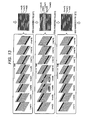
- FIG. 13 is an explanatory diagram of an image displayed in the interleave scanning mode.
- An image obtained by the imaging device 55 is displayed in the display section 15 (see FIGS. 1 and 4 ) with its fields switched in a short period of time in the order of an odd-numbered field F1, an even-numbered field F2, an odd-numbered field F3, etc.
- the odd-numbered field F1 includes 8 lines Line(1) through Line(15)
- the even-numbered field F2 includes 8 lines Line(2) through Line(16) as illustrated in FIG. 13 .
- An error caused due to influence of noise during the transmission of serial image data occurs at continuous timing from the viewpoint of the transmission order of the serial image data.
- transmitted signals correspond to interleave scanned data
- the error is not displayed over adjacent lines or over a plurality of fields continuous in a time series, Specifically, as illustrated in FIG. 13 , assuming that an error is caused during the transmission of the lines Line(6) and Line(8) of the even-numbered field F2, this error appears as an image having a loss of image information of the lines Line(6) and Line(8) of the even-numbered field F2.
- the normal scanning mode is switched to the interleave scanning mode in detecting an error occurring in transmitted serial data.
- FIG. 14 is a flowchart illustrating procedures in the switching to the interleave scanning mode
- FIG. 15 is a schematic block diagram conceptually illustrating the principal part of the endoscope system
- FIG. 16 is a timing chart illustrating timing of switching the normal scanning mode to the interleave scanning mode.
- the control circuit 143 (see FIG. 5 ) of the imaging device 55 conducts the scan in the normal scanning mode in which the lines extending along the main scanning direction are scanned and read in the sub scanning direction, so that the imaging signal SDT may be transmitted from the endoscope 100 to the processor section 69 through the signal line 113a as illustrated in FIG 15 .
- the imaging signal SDT has the aforementioned data format illustrated in FIG. 6 , and in this control method, occurrence of a transmission error is detected by utilizing information of the ECC (Error Check and Correct) region provided behind the payload including the image information.
- the CDR circuit 121 illustrated in FIG. 15 performs transmission error discrimination on the image information of the payload on the basis of the information of the ECC region (step S1).
- an error detection signal is sent to the CPU 115, so as to correct an error region (step S3).
- a field in which the error has been detected is scanned without switching the scanning mode until the scan of all the lines of this field is completed.
- the image processing circuit 129 converts transmitted video signals into two-dimensional image data and makes the display section 15 to display the data.
- the display section 15 displays the image regardless of the occurrence of an error, and the line having an error is displayed by a same color filling method in which the whole line is filled with the same color of gray or the like.
- step S4 when the image display of the field including the error region is completed (YES in step S4), the CPU 115 sends a mode switching signal to the register 103 of the endoscope 100, so as to switch the normal scanning mode to the interleave scanning mode (step S5). It is noted that the image information of the payload may be recovered if necessary in the correction of the error region performed in step S3.
- the control circuit 143 of the imaging device 55 reads charge signals of the unit pixels 131 (see FIG. 5 ) in the normal scanning mode, and the endoscope 100 serially transmits a video signal generated on the basis of the charge signals to the processor section 69.
- the CDR circuit 121 of the processor section 69 detects an error in the video signal during the transmission, namely, when an error detection signal Se is input to the CPU 115, the CPU 115 reads, still in the normal scanning mode, the charge signals of all the lines of an image of a field Fi where the error has been detected, so as to complete the serial transmission.
- the CPU 115 outputs a mode switching signal Sm for switching the scanning mode to the endoscope 100, and the control circuit 143 of the imaging device 55 of the endoscope 100 switches the scanning mode from the normal scanning mode to the interleave scanning mode on the basis of the mode switching signal Sm.
- the control circuit 143 reads the charge signals of a field F i+1 in the interleave scanning mode.
- the charge signals are read with the scanning mode switched to the interleave scanning mode from the field F i+1 next to the field where the error has been detected, and hence, the influence of noise may be made inconspicuous after the occurrence of the error.
- functions to detect, correct and compensate a transmission error are preferably provided in order to improve the noise resistance during the digital transmission.
- the function to detect an error not only the aforementioned ECC region but also cyclic redundancy check (CRC), invalid code detection (such as detection of a code undefined by the 8B10B encoding), invalid format detection or the like may be employed.
- FEC forward error correction
- BCH code As the function to correct an error, forward error correction (FEC) such as BCH code may be employed.
- FEC forward error correction
- any of various methods may be appropriately employed including not only the aforementioned overwriting method by the same color filling method but also previous line interpolation in which an error is interpolated by using a value of the previous line of the same frame, previous frame interpolation in which an error is interpolated by using a value of a line in the same position in the previous frame, or previous/following line interpolation in which an error is interpolated by using values of previous and following lines.
- the order of the signals of the respective lines may be changed by another method apart from the control of the reading order of the charge signals.
- the charge signals of the imaging device may be read in the normal scanning mode to be stored once in a memory, and the charge signals of the respective lines may be read from this memory in an order corresponding to that employed in the interleave scanning mode, so as to generate serial data.
- the scan read is conducted with one line interlaced in the interleave scanning mode of the aforementioned configuration example, the invention is not limited to this but two or more lines may be interlaced or lines may be randomly read.
- the imaging device is described as a CMOS image sensor, the imaging device is not limited to this but may be a CCD (Charge Coupled Device) image sensor when a memory is used together as described above.
- CCD Charge Coupled Device
- the driving part is set to the scanning mode in which the scan read with a prescribed number of lines interlaced along the sub scanning direction is repeated. According to the captured image signal generated in this scanning mode, a plurality of field screens formed with the prescribed number of lines interlaced are generated as sequential data.
- the loss is merely a loss of part of data continuous in the sequential data and never appears over lines adjacent to each other or over a plurality of field screens continuous in a time series in the captured image.
- lines adjacent to each other in a captured image are not continuously present and field screens continuous in a time series are not continuously present in a specific narrow data portion continuous in sequential data, and therefore, a lack of adjacent lines and a defect caused in field screens continuous in a time series, which are visually conspicuous, may be avoided.
- the loss of the data appears, for example, in a specific field screen alone, and the field screen having the loss is immediately replaced with a next field screen. Furthermore, the loss of the data never appears as adjacent lines in the captured image but appears in positions away from each other correspondingly to the prescribed number of lines.
- each of the scanning modes may be selectively employed, so as to switch the scanning mode at necessary timing for serially transmitting generated image data.
- the scanning mode is switched to a mode in which the image data transmission is minimally influenced by an error derived from the disturbance, and hence, the quality of a displayed image may be kept high.
- noise tends to be caused in a signal line in performing a treatment with a high frequency treatment instrument at timing of turning on the high frequency treatment instrument
- the first scanning mode is switched to the second scanning mode in this endoscope system
- the loss may be made visually inconspicuous.
- a good captured image may be always provided.
- the detection data is provided to every line, the occurrence of a transmission error may be detected with respect to every line, and hence, a line having an error may be easily recovered. Furthermore, since the first scanning mode is switched to the second scanning mode on the basis of the timing of the detection of the occurrence of a transmission error, an error occurring at arbitrary timing may be coped with at any time for switching an appropriate mode, and therefore, a good captured image may be always provided.
- control means switches the driving part from the first scanning mode to the second scanning mode before supplying a high frequency current to the high frequency treatment instrument.
- the driving part is switched to the second scanning mode before supplying the high frequency current to the high frequency treatment instrument, and therefore, a loss of data caused by the occurrence of noise may be made inconspicuous at timing at which noise tends to be caused in a signal line. Thus, a good captured image may be always stably supplied.
- control means switches the driving part from the first scanning mode to the second scanning mode after completing read scan of whole of the captured image in which the transmission error has been detected.
- the endoscope system of the invention includes an endoscope equipped with an imaging part for outputting a captured image signal of a subject; a controller separated from the endoscope and connected to the endoscope through a signal line, for serially transmitting digital image data including the captured image signal between the endoscope and the controller; and interleave image data generating means for generating interleave image data in which all horizontal lines of a captured image obtained based on the captured image signal of the subject are rearranged by rearranging some horizontal lines of the captured image with a prescribed number of lines interlaced along a vertical direction of the captured image and rearranging the other horizontal lines with the prescribed number of lines interlaced from one interlaced horizontal line.
- a loss of data caused by the occurrence of the transmission error may be made inconspicuous in the captured image not by employing a driving method in which the order of reading charge signals from the imaging part is changed but by employing a driving method performed in a normal successive order of lines.
Abstract
Description
- The present invention relates to an endoscope system.
- As a technology for signal transmission of a captured image between an endoscope and a controller connected to the endoscope, a system employing analog transmission is described in
JP-A-60-55923 - In the transmission of image information, it has been also proposed to digitalize the image information and serially transmit the digitalized information in order to reduce the image quality degradation caused during the transmission (see
JP-A-2009-201540 JP-A-2008-80007 - Therefore, even when a captured image signal is serially transmitted to the controller from the endoscope for reducing the degradation in the image quality, when noise externally influences during the transmission, the influence of the noise conspicuously appears in a displayed image.
- An object of the invention is providing an endoscope system capable of outputting high quality image information by making influence of noise inconspicuous even if a captured image signal is externally influenced by noise during serial transmission of the captured image signal from an endoscope to a controller.
- According to an aspect of the invention, an endoscope system includes:
- an endoscope including an imaging part that outputs a captured image signal of a subject; and
- a controller separated from the endoscope and connected to the endoscope through a signal line, the captured image signal output from the imaging part being serially transmitted as digital image data between the endoscope and the controller,
- wherein the imaging part includes a plurality of light receiving portions two-dimensionally arranged and a driving part that reads a charge signal stored in each of the light receiving portions,
- the driving part conducts read scan in which read of the charge signals from the light receiving portions arranged along each line extending in a main scanning direction corresponding to an arranging direction of the light receiving portions is repeated plurality of times along a sub scanning direction perpendicular to the main scanning direction, and
- the driving part changes an order of outputting the lines in the image data by conducting the read scan on all lines included in the captured image so as to scan some lines successively with a prescribed number of lines interlaced along the sub scanning direction and scan the other lines successively from an interlaced line with the prescribed number of lines interlaced.
-
-
FIG. 1 is a diagram illustrating the whole structure of an endoscope system including an endoscopic device for explaining an embodiment of the invention, -
FIG. 2 is an enlarged principal part cross-sectional view illustrating a tip part of the endoscopic device, -
FIG. 3 is a vertical principal part cross-sectional view roughly illustrating the structure of a high frequency treatment instrument, -
FIG. 4 is a conceptual block diagram of the endoscope system ofFIG. 1 , -
FIG. 5 is a circuit diagram illustrating the configuration of an imaging device, -
FIG. 6 is a schematic diagram illustrating a format of transmit data to be serially transmitted, -
FIG. 7 is a timing chart illustrating exposing/reading timing of the imaging device in a normal scanning mode, -
FIG. 8 is a diagram illustrating an example of a captured image, -
FIG. 9 is a timing chart illustrating exposing/reading timing of the imaging device in an interleave scanning mode of 1-line interlaced scan, -
FIG. 10 is a diagram illustrating a captured image generated in accordance with the reading order of charge signals in the interleave scanning mode ofFIG. 9 , -
FIG. 11 is a flowchart illustrating procedures in switching between the normal scanning mode and the interleave scanning mode, -
FIG. 12 is a timing chart illustrating timing of switching from the normal scanning mode to the interleave scanning mode, -
FIG. 13 is an explanation diagram of a displayed image obtained in the interleave scanning mode ofFIG. 9 , -
FIG. 14 is a flowchart illustrating procedures in switching to the interleave scanning mode, -
FIG. 15 is a conceptual block diagram illustrating a principal part of the endoscope system, and -
FIG. 16 is a timing chart illustrating timing of switching from the normal scanning mode to the interleave scanning mode ofFIG. 14 . - Now, a preferred embodiment of the invention will be described in detail with reference to the accompanying drawings.
-
FIG. 1 is a schematic diagram illustrating the whole structure of an endoscope system including an endoscopic device for explaining the embodiment of the invention. - The
endoscope system 200 includes the endoscopic device (hereinafter sometimes referred to as the endoscope) 100, acontroller 13 connected to theendoscope 100, adisplay section 15 such as a monitor, aninput section 17 such as a keyboard, atreatment instrument 71, a high frequencypower control section 97 for driving thetreatment instrument 71, and afoot switch 99 connected to the high frequencypower control section 97. Thecontroller 13 includes alight source section 67 for supplying theendoscope 100 with illumination light and aprocessor section 69 for subjecting an imaging signal supplied from theendoscope 100 to various image processing for converting it into a video signal. - The
endoscope 100 includes abody operating section 21, anendoscope inserting section 23 connected to thebody operating section 21 to be inserted into a body cavity, auniversal cord 25 connected to thebody operating section 21 and containing various duct lines and signal cables, andconnectors universal cord 25 to be removably connected to thecontroller 13. Theconnectors light source section 67 and theprocessor section 69 of thecontroller 13 or may be one connector of a composite type. - The
light source section 67 of thecontroller 13 outputs emitted light to theendoscope 100 through theconnector 27A and theuniversal cord 25, so that illumination light may be supplied to an illuminating optical system provided at the tip of theendoscope inserting section 23. - In the
body operating section 21 of theendoscope 100,various buttons 29 such as an air/water supply button, a suction button, a shutter button and a function switching button are arranged, and a pair ofangle nobs 31 for bending a tip side of the endoscope are provided. - The
endoscope inserting section 23 includes asoft part 33, abending part 35 and a tip part (an endoscope tip part) 37 successively disposed in this order from the side of thebody operating section 21. Thesoft part 33 is flexible and is connected to the base side of thebending part 35, and thebending part 35 is capable of bending when a wire (not shown) inserted through theendoscope inserting section 23 is pulled by rotating theangle nobs 31 of thebody operating section 21. As a result, theendoscope tip part 37 may be made to face toward a desired direction. -
FIG. 2 is an enlarged partial cross-sectional view illustrating the structure of the tip part of the endoscopic device. An imaging optical system provided at the tip of theendoscope inserting section 23 includes animaging chip 51 having animaging device 55 for capturing an image of an observed site illuminated by the illuminating optical system, and outputs an imaging signal of the observed image obtained from theimaging device 55 to thecontroller 13. As theimaging device 55, a CMOS (Complementary Metal Oxide Semiconductor) image sensor is used. Theprocessor section 69 of thecontroller 13 displays, in thedisplay section 15 illustrated inFIG. 1 , image information obtained through image processing of the input imaging signal. Theinput section 17 such as a keyboard connected to thecontroller 13 may be used for inputting commands for such a series of processing. - The
endoscope tip part 37 is provided with a lighting window (not shown) and an observation window 45 (seeFIG. 2 ) as well as a clamp opening 43 of aninstrument inserting hole 47. In theobservation window 45, an objectiveoptical system 49 including a plurality of lenses is provided for capturing an image of an observed site inside a body cavity. Behind the objectiveoptical system 49 along the optical path, aprism 53 is connected for bending the optical axis of the objectiveoptical system 49 at right angles to guide it toward theimaging chip 51. - The
imaging chip 51 is a monolithic semiconductor (i.e., what is called a CMOS sensor chip) integrally including theimaging device 55 and aperipheral circuit 57 for driving theimaging device 55 and for inputting/outputting signals to/from theimaging device 55, and is mounted on asubstrate 59. Asignal line 61 is connected to the rear end of thesubstrate 59, and thesignal line 61 is connected to theprocessor section 69 through theuniversal cord 25 illustrated inFIG. 1 so as to transfer various signals. In other words, the objectiveoptical system 49 and theprism 53 together form an optical image obtained on the side of theendoscope tip part 37 on theimaging device 55 of theimaging chip 51, and theimaging device 55 outputs an output signal of the optical image as a captured image signal. The captured image signal is transmitted from the side of theendoscope 100 to thecontroller 13 through theuniversal cord 25. - The
processor section 69 of thecontroller 13 subjects the captured image signal transmitted from theendoscope 100 to the image processing on the basis of a command issued from thebody operating section 21 or theinput part 17 of theendoscope 100, so as to generate an image for display to be supplied to thedisplay part 15. - A connecting
part 39 disposed between thebody operating section 21 and theendoscope inserting section 23 is provided with aclamp inserting section 41 through which a treatment instrument such as a clamp is inserted. Theaforementioned treatment instrument 71 is inserted through thisclamp inserting section 41 to be guided out from the tip of theendoscope tip part 37. Thetreatment instrument 71 is introduced to theendoscope tip part 37 through theinstrument inserting hole 47 formed through theendoscope inserting section 23 as illustrated inFIG 2 . Thetreatment instrument 71 is a high frequency treatment instrument that may superimpose noise on a signal line adjacently provided in this embodiment, and is connected to the high frequencypower control section 97 through anelectric cord 95. The high frequencypower control section 97 is connected to thecontroller 13 and thefoot switch 99 for controlling the drive of the highfrequency treatment instrument 71. - The structure of the high
frequency treatment instrument 71 will now be described. -
FIG. 3 is a vertical principal part cross-sectional view illustrating the schematic structure of the high frequency treatment instrument. As illustrated inFIG. 3 , the highfrequency treatment instrument 71, that is, a diathermy knife, has flexibility sufficient to be inserted into the treatmentinstrument inserting hole 47 of the endoscope 100 (seeFIG. 2 ) and includes a sheath 75 containing aclose wound coil 75a and an insulatingtube 75b of tetrafluoroethylene or the like covering theclose wound coil 75a, and anoperation part 77 provided at the base end of the sheath 75. At the tip of theclose wound coil 75a, acylindrical stopper member 79 and a ring-shaped sheathtip insulating chip 81 are provided to be covered with the insulatingtube 75b. - An
operation wire 83 with a conducting property is provided inside the sheath 75 to be movable along the shaft direction, and astopper receiving part 85 with a conducting property in contact with thestopper member 79 is attached to the tip of theoperation wire 83. Thestopper receiving part 85 is provided with and electrically connected to a highfrequency electrode part 73, that is, a knife part, including abar electrode 73 a and aplate electrode 73b. - The
operation part 77 of the highfrequency treatment instrument 71 includes anoperation shaft part 89 and aslider 91 slidable on theoperation shaft part 89. Theslider 91 is provided with aconnector part 93 and is connected to the high frequencypower control section 97 through theelectric cord 95. The high frequencypower control section 97 is connected to theswitch 99 such as a foot switch. - The base of the
operation wire 83 is extended backward through an insertion hole not shown formed in theoperation shaft part 89 so as to be connected to theslider 91. When theslider 91 is slid in the shaft direction, theoperation wire 83 moves backward/forward along the shaft direction inside the sheath 75, so that thebar electrode 73a of the highfrequency electrode part 73 may appear/disappear from the tip of the sheath 75. - Next, signal processing performed by the endoscope system having the aforementioned structure will be described.
-
FIG. 4 is a conceptual block diagram illustrating the configuration of the endoscope system. As illustrated inFIG. 4 , theendoscope system 200 includes theendoscope 100 and theprocessor section 69 connected to each other through theuniversal cord 25. Theimaging chip 51 including theimaging device 55 and theperipheral circuit 57 is built in theendoscope 100. Theperipheral circuit 57 of theimaging chip 51 includes a PLL (Phase-Locked Loop)circuit 101 for generating an internal clock signal, aregister 103 for setting control data in theimaging device 55, an analog/digital (A/D)converter 105 for digitalizing an imaging signal output from theimaging device 55, an 8B10B encoder 107 for subjecting the digitalized imaging signal to 8B10B type encoding, aPLL circuit 109 for generating a clock signal for serial transmission by multiplying the frequency of the internal clock signal, and a parallel/serial (P/S)converter 111 for converting the encoded imaging signal into a serial signal and outputting the serial signal. - The
PLL circuit 101 is a phase locked circuit composed of a phase comparator, a loop filter, a voltage control oscillator and a frequency divider, and generates an internal clock signal ICLK in synchronization with a stable reference clock signal BCLK input from theprocessor section 69 and having a frequency in a prescribed proportional relationship with the frequency of the reference clock signal BCLK (i.e., having a multiplied frequency). The internal clock signal ICLK is supplied to respective portions of theperipheral circuit 57 and theimaging device 55. - The
register 103 holds control data CTLD input from theprocessor section 69 and used for driving theimaging device 55 and inputs it to theimaging device 55. Theregister 103 is a shift register for performing serial/parallel conversion, and converts the control data CTLD input in the form of a serial signal into a parallel signal to be input to theimaging device 55. As the control data CTLD, a scanning method for pixels (such as a normal scanning or interleave scanning mode described in detail later), a pixel region to be scanned, a shutter speed (i.e., exposure time) and the like are input. Theimaging device 55 controls a scanning circuit described later on the basis of the control data CTLD and the internal clock signal ICLK. - The A/
D converter 105 converts the imaging signal output from theimaging device 55 through quantization into an 8-bit (256-scale) digital signal and inputs the converted 8-bit digital signal to the 8B10B encoder 107 in parallel by using 8 lines. - The 8B10B encoder 107 is an 8B10B type encoder for converting the 8-bit digital signal input from the A/
D converter 105 into a 10-bit digital signal by adding redundant 2-bit data, and the conversion from 8-bit to 10-bit is conducted by using a translation table according to a standard. - The
PLL circuit 109 has a similar configuration to thePLL circuit 101, and generates the clock signal TCLK for serial transmission by multiplying the frequency of the internal clock signal ICLK by, for example, 10 and supplies the clock signal TCLK to the P/S converter 111. - The P/
S converter 111 converts the digital signal (i.e., the 10-bit parallel data) input from the 8B10B encoder 107 into 10-bit serial data in accordance with the clock signal TCLK for serial transmission generated by thePLL circuit 109. At this point, owing to the function of thePLL circuit 109, the frequency of the serial data resulting from the conversion is 10 times as high as the frequency of the parallel data obtained before the conversion. The serial data generated by the P/S converter 111 is transmitted to theprocessor section 69 as an imaging signal SDT through asignal line 113a running inside theuniversal cord 25. - The
processor section 69 includes a main control circuit (CPU) 115 for controlling the whole device, apower circuit 117 for generating a power voltage VDD and a ground voltage VSS, areference clock generator 119 for generating the reference clock signal BCLK, a clock and data recovery (CDR)circuit 121 for receiving the imaging signal SDT from theimaging chip 51 and recovering a clock signal and a data signal from the imaging signal SDT, aPLL circuit 123 for generating a clock signal for signal processing with the same frequency as the internal clock signal ICLK used in theimaging chip 51 by multiplying the frequency of the clock signal generated by theCDR circuit 121, a serial/parallel (S/P)converter 125 for converting the data signal generated by theCDR circuit 121 into a parallel signal, an8B10B decoder 127 for generating the imaging signal obtained before the encoding by subjecting the parallelized imaging signal to 8B10B type decoding, and animage processing circuit 129 for generating image data to be displayed in thedisplay section 15 by subjecting the decoded imaging signal to the image processing. - The
power circuit 117 supplies the power voltage VDD and the ground voltage VSS to the respective portions within theprocessor section 69 and supplies these voltages to the respective portions within theimaging chip 51 through thesignal lines reference clock generator 119 generates the reference clock signal BCLK with a stable frequency and inputs the reference clock signal BCLK to thePLL circuit 101 included in theimaging chip 51 through asignal line 113d. - The
CPU 115 controls the respective portions within theprocessor section 69, generates the aforementioned control data CTLD and inputs the control data CTLD to theregister 103 included in theimaging chip 51 through asignal line 113e. - The
CDR circuit 121 detects the phase of the imaging signal SDT serially transmitted from theimaging chip 51, generates an extraction clock signal RCLK in synchronization with the frequency of the imaging signal SDT, and generates data obtained by retiming the imaging signal SDT with the extraction clock signal RCLK (i.e., retiming data or an imaging signal RSDT) by sampling the imaging signal SDT with the extraction clock signal RCLK. - The extraction clock signal RCLK generated by the
CDR circuit 121 is input to thePLL circuit 123, and the imaging signal RSDT generated by theCDR circuit 121 is input to the S/P converter 125. - The
PLL circuit 123 has a similar configuration to theaforementioned PLL circuit 101, and generates the clock signal SCLK for signal processing with the same frequency as the internal clock signal ICLK by multiplying the frequency of the extraction clock signal RCLK by 1/10. ThePLL circuit 123 supplies the thus generated clock signal SCLK to the S/P converter 125, the8B10B decoder 127 and theimage processing circuit 129. - The S/
P converter 125 subjects the imaging signal RSDT input from theCDR circuit 121 to serial/parallel conversion, corresponding to the inverse of the parallel/serial conversion, in accordance with the clock signal SCLK generated by thePLL circuit 123, so as to generate an imaging signal of 10-bit parallel data, and inputs the imaging signal to the8B10B decoder 127. - The
8B10B decoder 127 conducts conversion inverse to that performed by the aforementioned 8B10B encoder 107 by using a translation table according to the 8B10B standard, and decodes the imaging signal input thereto from the 10-bit signal to the 8-bit signal. The 8-bit imaging signal decoded by the8B10B decoder 127 is input to theimage processing circuit 129. - The
image processing circuit 129 records the imaging signal in an internal memory on the basis of the clock signal SCLK and generates image data to be output through various image processing including white balance adjustment, gain correction, color interpolation, edge enhancement, gamma correction, color matrix calculation and the like. Furthermore, theimage processing circuit 129 converts the image data into the form of a signal for displaying it in thedisplay section 15 and outputs the signal for image display to thedisplay section 15. - Moreover, as described above, the high frequency
power control section 97 is connected to the highfrequency treatment instrument 71, theCPU 115 and theswitch 99, and when a foot operation of theswitch 99 is conducted, a high frequency current is supplied to the highfrequency treatment instrument 71 on the basis of a command issued by theCPU 115. In other words, as illustrated inFIG. 3 , the high frequency current is supplied to the highfrequency electrode part 73 through theoperation wire 83 disposed inside the sheath 75 of the highfrequency treatment instrument 71. In supplying the high frequency current, the sheath 75 is in a state inserted through theinstrument inserting hole 47 of theendoscope 100, and therefore, noise tends to be superimposed onto thesignal line 113a adjacently disposed within the endoscope inserting section 23 (seeFIG. 1 ) along theinstrument inserting hole 47. In the configuration of this embodiment, even if the noise influences serial data to be transmitted, the degradation in image quality of a displayed image caused by the noise may be made inconspicuous by a method described later. - Next, signal processing for generating an imaging signal by taking out a charge signal from each pixel of the
imaging device 55 will be described. -
FIG. 5 is a circuit diagram schematically illustrating the configuration of theimaging device 55. As illustrated inFIG. 5 , theimaging device 55 includes apixel part 133 in whichunit pixels 131, that is, light receiving portions, are arranged in the form of a two-dimensional matrix, a correlated double sampling (CDS)circuit 135 for performing noise suppressing processing or the like on a charge signal corresponding to an output signal from thepixel part 133, avertical scanning circuit 137 for controlling scan of thepixel part 133 in the vertical direction and controlling a reset operation of thepixel part 133, ahorizontal scanning circuit 139 for controlling scan along the horizontal direction, anoutput circuit 141 for outputting a charge signal having been read, and acontrol circuit 143 for supplying a control signal to each of thecircuits 135 through 139 and controlling timing and the like of the vertical/horizontal scan and sampling. - Each
unit pixel 131 includes one photodiode D1, a transistor M1 for reset, a transistor M2 for drive (amplification) and a transistor M3 for pixel selection. Eachunit pixel 131 is connected to a vertical scanning line (row selecting line) L1 and a horizontal scanning line (column selecting line) L2, and theunit pixels 131 are successively scanned by thevertical scanning circuit 137 and thehorizontal scanning circuit 139. - The
control circuit 143 generates a control signal to be input to thevertical scanning circuit 137 and thehorizontal scanning circuit 139 for scanning the rows and the columns of thepixel part 133, a control signal to be input to thevertical scanning circuit 137 for resetting charge stored in each photodiode D1, and a control signal to be input to theCDS circuit 135 for controlling connection between thepixel part 133 and theCDS circuit 135. - The
CDS circuit 135 is provided correspondingly to each column selecting line L2, so as to successively output, in accordance with a horizontal scanning signal output by thehorizontal scanning circuit 139, charge signals of therespective unit pixels 131 connected to a column selecting line L1 selected by thevertical scanning circuit 137. Thehorizontal scanning circuit 139 controls, in accordance with the horizontal scanning signal, an on/off state of a transistor M4 for column selection provided between theCDS circuit 135 and an output bus line L3 connected to theoutput circuit 141. Theoutput circuit 141 amplifies the charge signals successively sent from theCDS circuit 135 to the output bus line L3 and outputs the amplified signals. In the description given below, a signal output from theoutput circuit 141 is designated as an imaging signal for distinguishing it from a charge signal read from eachunit pixel 131. - Although not shown in the drawings, the
imaging device 55 is a single chip color sensor type imaging device including a color filter (such as a Bayer primary color filter) including a plurality of color segments. - The
pixel part 133 has a square array structure in which theunit pixels 131 are arranged in the form of a matrix along the row direction and the column direction on a semiconductor substrate, wherein the column direction is the vertical direction and the row direction is the horizontal direction. Alternatively, it may have what is called honeycomb pixel arrangement in whichunit pixels 131 disposed on odd-numbered rows andunit pixels 131 disposed on even-numbered rows are shifted from each other by a half pitch. - When the inside of a body cavity is observed with the
endoscope system 200 having the aforementioned structure, as illustrated inFIG. 4 , an imaging signal generated by theimaging device 55 is converted into an 8-bit parallel signal by the A/D converter 105 and then converted into a 10-bit parallel signal by the 8B10B encoder 107. The imaging signal of the 10-bit parallel signal is converted into a serial signal by the P/S converter 111 and then transmitted to theprocessor section 69 through thesignal line 113a. - The
processor section 69 receives the serially transmitted imaging signal at theCDR circuit 121, so that theCDR circuit 121 may generate a clock signal (i.e., an extraction clock signal RCLK) and a data signal phase locked with the clock signal (i.e., retiming data RSDT). The imaging signal RSDT generated as the retiming data by theCDR circuit 121 is converted on the basis of the extraction clock signal RCLK by the S/P converter 125 and the8B10B decoder 127 so as to be recovered to the original 8-bit parallel signal. The imaging signal of this 8-bit parallel signal is converted into image data by theimage processing circuit 129, so that a captured image may be displayed in thedisplay section 15. -
FIG. 6 illustrates an example of the format of transmit data serially transmitted. A charge signal output from theoutput circuit 141 is converted into serial data of this format by theperipheral circuit 57 of theimaging device 55 so as to be transmitted to theprocessor section 69. The serial data has a header region in front of payload including image information and an ECC (Error Check and Correct) region corresponding to detection data and an idle region behind the payload.FIG. 6 illustrates the content corresponding to one line of a captured image, and a plurality of data each corresponding to one line are serially transmitted. The information of the ECC region is provided for detecting a transmission error. Furthermore, since the detection data is attached to every line, a transmission error may be detected with respect to every line, and hence, a line having an error may be easily recovered. - Next, a method for taking out a charge signal in the
imaging device 55 having the aforementioned configuration will be described in detail with reference toFIGS. 7 through 10 . - The
imaging device 55 may be set selectively to a normal scanning mode and an interleave scanning mode in accordance with a command issued by the CPU 115 (seeFIG. 4 ) of theprocessor section 69. In the normal scanning mode, scan/read of charge signals from the respective lines of the unit pixels (photodiodes) 131 arranged in the main scanning direction is successively performed along the sub scanning direction, so as to read charge signals from the respective lines. In the interleave scanning mode, scan/read of the lines of theunit pixels 131 performed along the sub scanning direction with a prescribed number of lines interlaced is successively repeated, so as to horizontally scan all the lines for reading the charge signals. - As illustrated in an exposing/reading timing chart of
FIG. 7 for the imaging device in the normal scanning mode, in a CMOS sensor including pixel rows corresponding to scanning lines Line(1) through Line(n) (wherein n is an integer not less than 2), exposure of photodiodes is started after resetting respective unit pixels (0 through m) of each line, and after a prescribed exposure time, charge stored in the respective photodiodes is transferred for outputting charge signals. This operation is conducted successively from the scanning line Line(1) to the scanning line Line(n) in a delayed manner. In other words, in this mode, the scan/read of the respective lines of unit pixels arranged along the main scanning direction is successively conducted along the sub scanning direction for reading the charge signals, so as to generate a captured image of n rows and m columns. - Assuming that the content of a captured image is a letter "A", when signals output onto the output bus line L3 by repeating the scan of unit pixels along the main scanning direction from an image origin P0 and the scan along the sub scanning direction are changed into image data in the output order, an image as illustrated in
FIG. 8 is obtained. -
FIG. 9 illustrates an example of resetting, exposing and reading timings for an imaging device using a rolling shutter in a 1-line interlaced scanning mode, that is, a kind of the interleave scanning mode. As illustrated inFIG. 9 , a reset signal is output to each transistor M1 for reset (seeFIG. 5 ) of the scanning line Line(1) from thevertical scanning circuit 137, so as to reset charge stored in the respective photodiodes D1 disposed on the scanning line Line(1) and to start charge storage (exposure). Thereafter, with one line interlaced along the vertical direction (i.e., the sub scanning direction), the scanning line Line(3) is reset and started to be charged in the same manner. Furthermore, with one line interlaced along the vertical direction, the scanning line Line(5) is reset and started to be charged, and such an operation is repeatedly conducted. - When there is no line to be interlaced, the scan starts from the scanning line Line(2) again, and after resetting the scanning line Line(2) and starting the charge storage thereof, one line is interlaced along the vertical direction, and the scanning line Line(4) is reset. Such reset processing is repeated up to the scanning line Line(n) (wherein n is the total number of the scanning lines). In this manner, charge signals stored in the
unit pixels 131 of the respective lines are once discharged, and thereafter, the charge storage is started. - After a prescribed charge storage time, charge signals stored in the
unit pixels 131 are output to the CDS circuit 135 (seeFIG. 5 ). Therefore, in accordance with a selection signal to each transistor M3 for pixel selection input through the row selecting line L1 and a reading signal input from each column selecting transistor M4 for column selection input through the column selecting line L2, the charge signals of therespective unit pixels 131 are output to the output bus line L3 (seeFIG. 5 ) in the order of scanning lines Line(1), Line(3), ..., Line(n-1), Line(2), Line(4), ..., and Line(n). - In other words, in this interleave scanning mode, first read scan in which a first line not scanned yet is selected for horizontal scan for reading charge signals from respective light receiving portions corresponding to the first line and second read scan in which a second line not scanned yet interlaced by a prescribed number of lines from the first line along the sub scanning direction is selected for the horizontal scan for reading charge signals from respective light receiving portions corresponding to the second line are repeated down to the lower end of the sub scanning direction while keeping the prescribed number of lines as the interval between the first line and the second line, and thereafter, the first read scan and the second read scan are repeated down to the lower end of the sub scanning direction again with a line not scanned yet selected from the upper end of the sub scanning direction, and such a process is repeated plural times.
- Assuming that the content of a captured image is a letter "A" as illustrated in
FIG. 8 , in the case where the aforementioned output order of the charge signals is employed, when signals output onto the output bus line L3 by repeating the scan along the main scanning direction from an image origin P0 and the scan with one line interlaced along the sub scanning direction are changed into image data in the output order, image data halved along the sub scanning direction as illustrated inFIG. 10 is obtained. - In other words, the signals are output in a time series in the successive and continuous order of the respective lines of a captured image in the sub scanning direction in the normal scanning mode, while the signals are output in the discontinuous order of the lines in a captured image in the interleave scanning mode. Therefore, in the interleave scanning mode, even when an error is caused in part of an imaging signal during the transmission, a region having the error appears as discontinuous lines not adjacent to each other in a displayed image, and hence, degradation of the image quality caused by the error is inconspicuous.
-
FIG. 11 is a flowchart illustrating procedures in switching between the normal scanning mode and the interleave scanning mode. In the case where influence of external noise is feared during the transmission of serial data, the normal scanning mode is switched to the interleave scanning mode. This mode switching is conducted at timing of the operation of the highfrequency treatment instrument 71 for eliminating the influence of noise caused during the operation of the highfrequency treatment instrument 71. Specifically, since a high frequency current is applied for operating the highfrequency treatment instrument 71 while theswitch 99 is in an on state, the interleave scanning mode is set during the on operation. - In
FIG. 11 , the normal scanning mode is set for capturing an image in step S1, it is determined in step S2 whether or not theswitch 99 is in an on state (namely, whether or not the switch has been operated), and when it is in an off state, it is determined that the highfrequency treatment instrument 71 is not operated and hence the normal scanning mode is retained. When it is determined that theswitch 99 is in an on state, the normal scanning mode is switched to the interleave scanning mode in step S3. After switching to the interleave scanning mode, a high frequency current is applied to the highfrequency treatment instrument 71 in step S4, so as to perform a treatment such as incision of a tissue. Subsequently, it is determined in step S5 whether or not theswitch 99 is in an off state, and when it is in an on state, the interleave scanning mode is retained. When it is in an off state, it is determined that the treatment with the highfrequency treatment instrument 71 has been completed, and hence the interleave scanning mode is switched to the normal scanning mode in step S6. -
FIG. 12 is a timing chart illustrating timing of switching the normal scanning mode to the interleave scanning mode under control as illustrated inFIG. 11 . When theswitch 99 is operated to be placed in an on state, theCPU 115 detects the on state and hence sends a mode switching signal to the register 103 (seeFIG. 4 ), so as to switch the normal scanning mode to the interleave scanning mode. After completing the mode switching, the high frequencypower control section 97 applies a high frequency current to the highfrequency treatment instrument 71. In this manner, prior to the application of the high frequency current to the highfrequency treatment instrument 71, the switching from the normal scanning mode to the interleave scanning mode is completed, and therefore, the influence of high frequency noise on a displayed image is definitely reduced. -
FIG. 13 is an explanatory diagram of an image displayed in the interleave scanning mode. An image obtained by theimaging device 55 is displayed in the display section 15 (seeFIGS. 1 and4 ) with its fields switched in a short period of time in the order of an odd-numbered field F1, an even-numbered field F2, an odd-numbered field F3, etc. At this point, it is assumed for simplifying the description that one frame image includes 16 lines, that the odd-numbered field F1 includes 8 lines Line(1) through Line(15) and that the even-numbered field F2 includes 8 lines Line(2) through Line(16) as illustrated inFIG. 13 . - An error caused due to influence of noise during the transmission of serial image data occurs at continuous timing from the viewpoint of the transmission order of the serial image data. In the case where transmitted signals correspond to interleave scanned data, when the data is displayed in the
display section 15, the error is not displayed over adjacent lines or over a plurality of fields continuous in a time series, Specifically, as illustrated inFIG. 13 , assuming that an error is caused during the transmission of the lines Line(6) and Line(8) of the even-numbered field F2, this error appears as an image having a loss of image information of the lines Line(6) and Line(8) of the even-numbered field F2. - In displaying the even-numbered field F2, however, since an after image of the previous odd-numbered field F1 visually remains, information of the lines Line(5), Line(7) and Line(9) free from the error is substantially displayed before and after the lines Line(6) and Line(8). Therefore, the lines Line(6) and Line(8) having a loss due to the error are not displayed adjacent to each other (as upper and lower lines continuous along the sub scanning direction) in the screen but are displayed in a state sandwiched between the lines free from the error. Furthermore, immediately after the display timing of the even-numbered field F2 having the error, the screen of the next odd-numbered field and successively the screen of the next even-numbered field are replaced to be displayed. Therefore, even when an error is caused, a loss minimally appears continuously over a plurality of fields continuous in a time series, and even if the loss is continuously displayed over a plurality of fields, it appears in different positions on the screen, and hence, the error is never visually recognized conspicuously. Accordingly, even if an error is caused in part of data due to the influence of noise, it may be made visually inconspicuous.
- Another example of the control method for the endoscope system will now be described with reference to
FIGS. 14 through 16 . In theendoscope system 200 controlled by this method, the normal scanning mode is switched to the interleave scanning mode in detecting an error occurring in transmitted serial data. -
FIG. 14 is a flowchart illustrating procedures in the switching to the interleave scanning mode,FIG. 15 is a schematic block diagram conceptually illustrating the principal part of the endoscope system andFIG. 16 is a timing chart illustrating timing of switching the normal scanning mode to the interleave scanning mode. The procedures in this control method will now be described with reference to the flowchart ofFIG. 14 . In this control method, the control circuit 143 (seeFIG. 5 ) of theimaging device 55 conducts the scan in the normal scanning mode in which the lines extending along the main scanning direction are scanned and read in the sub scanning direction, so that the imaging signal SDT may be transmitted from theendoscope 100 to theprocessor section 69 through thesignal line 113a as illustrated inFIG 15 . The imaging signal SDT has the aforementioned data format illustrated inFIG. 6 , and in this control method, occurrence of a transmission error is detected by utilizing information of the ECC (Error Check and Correct) region provided behind the payload including the image information. Specifically, on the receiving side of the data transmission, theCDR circuit 121 illustrated inFIG. 15 performs transmission error discrimination on the image information of the payload on the basis of the information of the ECC region (step S1). When an error is detected (YES in step S2), an error detection signal is sent to theCPU 115, so as to correct an error region (step S3). At this point, a field in which the error has been detected is scanned without switching the scanning mode until the scan of all the lines of this field is completed. - The
image processing circuit 129 converts transmitted video signals into two-dimensional image data and makes thedisplay section 15 to display the data. Thedisplay section 15 displays the image regardless of the occurrence of an error, and the line having an error is displayed by a same color filling method in which the whole line is filled with the same color of gray or the like. - Subsequently, when the image display of the field including the error region is completed (YES in step S4), the
CPU 115 sends a mode switching signal to theregister 103 of theendoscope 100, so as to switch the normal scanning mode to the interleave scanning mode (step S5). It is noted that the image information of the payload may be recovered if necessary in the correction of the error region performed in step S3. - The aforementioned procedures will be described with reference to the timing chart of
FIG. 16 . - The
control circuit 143 of theimaging device 55 reads charge signals of the unit pixels 131 (seeFIG. 5 ) in the normal scanning mode, and theendoscope 100 serially transmits a video signal generated on the basis of the charge signals to theprocessor section 69. When theCDR circuit 121 of theprocessor section 69 detects an error in the video signal during the transmission, namely, when an error detection signal Se is input to theCPU 115, theCPU 115 reads, still in the normal scanning mode, the charge signals of all the lines of an image of a field Fi where the error has been detected, so as to complete the serial transmission. Thereafter, when the transmission of the image of the field Fi is completed, theCPU 115 outputs a mode switching signal Sm for switching the scanning mode to theendoscope 100, and thecontrol circuit 143 of theimaging device 55 of theendoscope 100 switches the scanning mode from the normal scanning mode to the interleave scanning mode on the basis of the mode switching signal Sm. After the mode switching, thecontrol circuit 143 reads the charge signals of a field Fi+1 in the interleave scanning mode. - In this manner, the charge signals are read with the scanning mode switched to the interleave scanning mode from the field Fi+1 next to the field where the error has been detected, and hence, the influence of noise may be made inconspicuous after the occurrence of the error.
- In the format of the serial data, functions to detect, correct and compensate a transmission error are preferably provided in order to improve the noise resistance during the digital transmission. As the function to detect an error, not only the aforementioned ECC region but also cyclic redundancy check (CRC), invalid code detection (such as detection of a code undefined by the 8B10B encoding), invalid format detection or the like may be employed.
- As the function to correct an error, forward error correction (FEC) such as BCH code may be employed. For an error that may not be corrected by the FEC, any of various methods may be appropriately employed including not only the aforementioned overwriting method by the same color filling method but also previous line interpolation in which an error is interpolated by using a value of the previous line of the same frame, previous frame interpolation in which an error is interpolated by using a value of a line in the same position in the previous frame, or previous/following line interpolation in which an error is interpolated by using values of previous and following lines.
- The present invention is not limited to the aforementioned embodiment but it is to be understood by those skilled in the art that various changes and modifications may be made in the invention without departing from the spirit and scope thereof.
- For example, although the above-described serial data is generated in the interleave scanning mode in which the order of reading the charge signals of the imaging device is changed, the order of the signals of the respective lines may be changed by another method apart from the control of the reading order of the charge signals. For example, the charge signals of the imaging device may be read in the normal scanning mode to be stored once in a memory, and the charge signals of the respective lines may be read from this memory in an order corresponding to that employed in the interleave scanning mode, so as to generate serial data.
- Furthermore, although the scan read is conducted with one line interlaced in the interleave scanning mode of the aforementioned configuration example, the invention is not limited to this but two or more lines may be interlaced or lines may be randomly read.
- Moreover, although the imaging device is described as a CMOS image sensor, the imaging device is not limited to this but may be a CCD (Charge Coupled Device) image sensor when a memory is used together as described above.
- As described so far, the following are herein disclosed:
- (1) According to an aspect of the invention, an endoscope system includes:
- an endoscope including an imaging part that outputs a captured image signal of a subject; and
- a controller separated from the endoscope and connected to the endoscope through a signal line, the captured image signal output from the imaging part being serially transmitted as digital image data between the endoscope and the controller,
- wherein the imaging part includes a plurality of light receiving portions two-dimensionally arranged and a driving part that reads a charge signal stored in each of the light receiving portions,
- the driving part conducts read scan in which read of the charge signals from the light receiving portions arranged along each line extending in a main scanning direction corresponding to an arranging direction of the light receiving portions is repeated plurality of times along a sub scanning direction perpendicular to the main scanning direction, and
- the driving part changes an order of outputting the lines in the image data by conducting the read scan on all lines included in the captured image so as to scan some lines successively with a prescribed number of lines interlaced along the sub scanning direction and scan the other lines successively from an interlaced line with the prescribed number of lines interlaced.
- In this endoscope system, digital image data serialized by changing the output order of the respective lines is transmitted, and hence, even when an error is caused in part of the data during the transmission due to influence of noise, the error thus caused may be made visually inconspicuous. Specifically, the driving part is set to the scanning mode in which the scan read with a prescribed number of lines interlaced along the sub scanning direction is repeated. According to the captured image signal generated in this scanning mode, a plurality of field screens formed with the prescribed number of lines interlaced are generated as sequential data. In the case where a loss is caused in the captured image signal because of an error occurring in part of the sequential data, the loss is merely a loss of part of data continuous in the sequential data and never appears over lines adjacent to each other or over a plurality of field screens continuous in a time series in the captured image. In other words, lines adjacent to each other in a captured image are not continuously present and field screens continuous in a time series are not continuously present in a specific narrow data portion continuous in sequential data, and therefore, a lack of adjacent lines and a defect caused in field screens continuous in a time series, which are visually conspicuous, may be avoided. Accordingly, when the captured image signal including the error and having been serially transmitted is displayed, the loss of the data appears, for example, in a specific field screen alone, and the field screen having the loss is immediately replaced with a next field screen. Furthermore, the loss of the data never appears as adjacent lines in the captured image but appears in positions away from each other correspondingly to the prescribed number of lines.
- (2) In the endoscope system of (1), the driving part is switched between (i) a first scanning mode in which the scan read is conducted successively on every line along the sub scanning direction and (ii) a second scanning mode in which the scan read is conducted on all the lines included in the captured image by scanning some lines successively with a prescribed number of lines interlaced along the sub scanning direction and scanning the other lines successively from an interlaced line with the prescribed number of lines interlaced.
- In this endoscope system, since the first scanning mode and the second scanning mode may be freely switched, each of the scanning modes may be selectively employed, so as to switch the scanning mode at necessary timing for serially transmitting generated image data.
- (3) The endoscope system of (1) or (2), may further include a disturbance detecting unit that detects disturbance that is an error occurrence factor during the serial transmission; and
- a controlling unit that switches the driving part from the first scanning mode to the second scanning mode when the disturbance detecting unit detects occurrence of disturbance.
- In this endoscope system, when disturbance occurs, the scanning mode is switched to a mode in which the image data transmission is minimally influenced by an error derived from the disturbance, and hence, the quality of a displayed image may be kept high.
- (4) In the endoscope system of (3), the disturbance detecting unit detects application timing of a high frequency current to a high frequency treatment instrument that is inserted into the subject together with an inserting portion of the endoscope and has a high frequency electrode exposed at a tip thereof, and
- the controlling unit switches the driving part from the first scanning mode to the second scanning mode based on the application timing of the high frequency current detected by the disturbance detecting unit.
- Although noise tends to be caused in a signal line in performing a treatment with a high frequency treatment instrument at timing of turning on the high frequency treatment instrument, when the first scanning mode is switched to the second scanning mode in this endoscope system, even if a loss of data is caused by the occurrence of noise, the loss may be made visually inconspicuous. As a result, regardless of the operation of the high frequency treatment instrument, a good captured image may be always provided.
- (5) In the endoscope system of (3) or (4), in the digital image data serially transmitted, the captured image signal is divided correspondingly to each of the lines and detection data that detects a transmission error is provided to every divided line, and
- the controlling unit detects occurrence of a transmission error by using the detection data and switches the driving part from the first scanning mode to the second scanning mode on the basis of timing of detecting the transmission error.
- In this endoscope system, since the detection data is provided to every line, the occurrence of a transmission error may be detected with respect to every line, and hence, a line having an error may be easily recovered. Furthermore, since the first scanning mode is switched to the second scanning mode on the basis of the timing of the detection of the occurrence of a transmission error, an error occurring at arbitrary timing may be coped with at any time for switching an appropriate mode, and therefore, a good captured image may be always provided.
- (6) In the endoscope system of (1) through (5), the prescribed number of lines to be interlaced is one line interlaced.
- In this endoscope system, since the scan read is conducted alternately on every line, a field of odd-numbered lines and a field of even-numbered lines are alternately obtained. Therefore, an image may be displayed according to a normal NTSC display method.
- (7) The endoscope system of (1) through (5), may further include: a display part that displays image information obtained based on the captured image signal serially transmitted.
- In this endoscope system, obtained information of a captured image may be displayed in the display part in a state where a loss of data is minimally conspicuous.
- In the endoscope system, the control means switches the driving part from the first scanning mode to the second scanning mode before supplying a high frequency current to the high frequency treatment instrument.
- In this endoscope system, the driving part is switched to the second scanning mode before supplying the high frequency current to the high frequency treatment instrument, and therefore, a loss of data caused by the occurrence of noise may be made inconspicuous at timing at which noise tends to be caused in a signal line. Thus, a good captured image may be always stably supplied.
- In the endoscope system, the control means switches the driving part from the first scanning mode to the second scanning mode after completing read scan of whole of the captured image in which the transmission error has been detected.
- In this endoscope system, since the driving part is switched to the second scanning mode after completing the read scan of the captured image in which the transmission error has been detected, a loss of data caused by the occurrence of the transmission error may be made inconspicuous in the captured image transmitted after the occurrence of the transmission error without complicating the read scan process. Thus, a good captured image may be stably supplied.
- The endoscope system of the invention includes an endoscope equipped with an imaging part for outputting a captured image signal of a subject; a controller separated from the endoscope and connected to the endoscope through a signal line, for serially transmitting digital image data including the captured image signal between the endoscope and the controller; and interleave image data generating means for generating interleave image data in which all horizontal lines of a captured image obtained based on the captured image signal of the subject are rearranged by rearranging some horizontal lines of the captured image with a prescribed number of lines interlaced along a vertical direction of the captured image and rearranging the other horizontal lines with the prescribed number of lines interlaced from one interlaced horizontal line.
- In this endoscope system, a loss of data caused by the occurrence of the transmission error may be made inconspicuous in the captured image not by employing a driving method in which the order of reading charge signals from the imaging part is changed but by employing a driving method performed in a normal successive order of lines.
Claims (7)
- An endoscope system comprising:an endoscope including an imaging part that outputs a captured image signal of a subject; anda controller separated from the endoscope and connected to the endoscope through a signal line, the captured image signal output from the imaging part being serially transmitted as digital image data between the endoscope and the controller,wherein the imaging part includes a plurality of light receiving portions two-dimensionally arranged and a driving part that reads a charge signal stored in each of the light receiving portions,the driving part conducts read scan in which read of the charge signals from the light receiving portions arranged along each line extending in a main scanning direction corresponding to an arranging direction of the light receiving portions is repeated plurality of times along a sub scanning direction perpendicular to the main scanning direction, andthe driving part changes an order of outputting the lines in the image data by conducting the read scan on all lines included in the captured image so as to scan some lines successively with a prescribed number of lines interlaced along the sub scanning direction and scan the other lines successively from an interlaced line with the prescribed number of lines interlaced.
- The endoscope system according to claim 1,
wherein the driving part is switched between (i) a first scanning mode in which the scan read is conducted successively on every line along the sub scanning direction and (ii) a second scanning mode in which the scan read is conducted on all the lines included in the captured image by scanning some lines successively with a prescribed number of lines interlaced along the sub scanning direction and scanning the other lines successively from an interlaced line with the prescribed number of lines interlaced. - The endoscope system according to claim 1 or 2, further comprising:a disturbance detecting unit that detects disturbance that is an error occurrence factor during the serial transmission; anda controlling unit that switches the driving part from the first scanning mode to the second scanning mode when the disturbance detecting unit detects occurrence of disturbance.
- The endoscope system according to claim 3,
wherein the disturbance detecting unit detects application timing of a high frequency current to a high frequency treatment instrument that is inserted into the subject together with an inserting portion of the endoscope and has a high frequency electrode exposed at a tip thereof, and
the controlling unit switches the driving part from the first scanning mode to the second scanning mode based on the application timing of the high frequency current detected by the disturbance detecting unit. - The endoscope system according to claim 3 or 4,
wherein in the digital image data serially transmitted, the captured image signal is divided correspondingly to each of the lines and detection data that detects a transmission error is provided to every divided line, and
the controlling unit detects occurrence of a transmission error by using the detection data and switches the driving part from the first scanning mode to the second scanning mode on the basis of timing of detecting the transmission error. - The endoscope system according to any of claims 1 through 5,
wherein the prescribed number of lines to be interlaced is one line interlaced. - The endoscope system according to any of claims 1 through 6, further comprising:a display part that displays image information obtained based on the captured image signal serially transmitted.
Applications Claiming Priority (1)
| Application Number | Priority Date | Filing Date | Title |
|---|---|---|---|
| JP2010130220A JP5463210B2 (en) | 2010-06-07 | 2010-06-07 | Endoscope system |
Publications (2)
| Publication Number | Publication Date |
|---|---|
| EP2392252A1 true EP2392252A1 (en) | 2011-12-07 |
| EP2392252B1 EP2392252B1 (en) | 2017-08-16 |
Family
ID=44509767
Family Applications (1)
| Application Number | Title | Priority Date | Filing Date |
|---|---|---|---|
| EP11168803.2A Not-in-force EP2392252B1 (en) | 2010-06-07 | 2011-06-06 | Endoscope system with interlaced image transmission |
Country Status (4)
| Country | Link |
|---|---|
| US (1) | US8902304B2 (en) |
| EP (1) | EP2392252B1 (en) |
| JP (1) | JP5463210B2 (en) |
| CN (1) | CN102283625B (en) |
Cited By (2)
| Publication number | Priority date | Publication date | Assignee | Title |
|---|---|---|---|---|
| JP2016527823A (en) * | 2013-08-02 | 2016-09-08 | ゼネラル・エレクトリック・カンパニイ | System and method for embedded imaging clocking |
| EP2743887A3 (en) * | 2012-12-14 | 2017-01-04 | FUJIFILM Corporation | Endoscope apparatus and image processing method thereof |
Families Citing this family (20)
| Publication number | Priority date | Publication date | Assignee | Title |
|---|---|---|---|---|
| US9622650B2 (en) | 2011-05-12 | 2017-04-18 | DePuy Synthes Products, Inc. | System and method for sub-column parallel digitizers for hybrid stacked image sensor using vertical interconnects |
| JP2013000452A (en) * | 2011-06-20 | 2013-01-07 | Olympus Corp | Electronic endoscope device |
| CH705952B1 (en) * | 2011-12-23 | 2017-06-15 | Awaiba Consultadoria Desenvolvimento E Comércio De Componentes Microelectrónicos Unipessoal Lda | Endoscope arrangement. |
| MX344146B (en) | 2012-07-26 | 2016-12-07 | Depuy Synthes Products Inc | Camera system with minimal area monolithic cmos image sensor. |
| JP6164836B2 (en) * | 2012-12-25 | 2017-07-19 | Hoya株式会社 | Endoscope |
| US10750933B2 (en) | 2013-03-15 | 2020-08-25 | DePuy Synthes Products, Inc. | Minimize image sensor I/O and conductor counts in endoscope applications |
| AU2014233190B2 (en) * | 2013-03-15 | 2018-11-01 | DePuy Synthes Products, Inc. | Image sensor synchronization without input clock and data transmission clock |
| JP6389352B2 (en) * | 2013-08-13 | 2018-09-12 | Hoya株式会社 | Endoscope system |
| WO2015029856A1 (en) * | 2013-08-27 | 2015-03-05 | オリンパスメディカルシステムズ株式会社 | Processing device and endoscope system |
| CN103873830B (en) * | 2014-03-20 | 2017-12-08 | 郑州赛福特电子设备有限公司 | Fujinon electronic video endoscope image system and fujinon electronic video endoscope image processing method |
| JP2015185823A (en) * | 2014-03-26 | 2015-10-22 | ソニー株式会社 | Solid state image sensor and imaging device |
| JP6151850B2 (en) * | 2014-03-28 | 2017-06-21 | 富士フイルム株式会社 | Endoscope system, processor device for endoscope system, and method for operating endoscope system |
| CN106999018A (en) * | 2014-12-19 | 2017-08-01 | 波士顿科学国际有限公司 | Imaging device and correlation technique |
| WO2019064681A1 (en) * | 2017-09-29 | 2019-04-04 | オリンパス株式会社 | Endoscope and endoscope system |
| WO2019181064A1 (en) * | 2018-03-23 | 2019-09-26 | オリンパス株式会社 | Endoscope |
| CN109820471B (en) * | 2019-02-27 | 2024-01-23 | 中国科学院苏州生物医学工程技术研究所 | Confocal endoscopic imaging dislocation correction system and method |
| CN110769207B (en) * | 2019-11-19 | 2022-04-01 | 深圳开立生物医疗科技股份有限公司 | Electronic endoscope signal transmission method, device, equipment and system |
| DE102020104634B4 (en) * | 2020-02-21 | 2023-12-28 | Excelitas Pco Gmbh | Method for reading out image data and for detecting an object, image recording device and light sheet microscope |
| WO2023275177A1 (en) * | 2021-06-30 | 2023-01-05 | Ambu A/S | Video processing apparatus with noise effect mitigation |
| CN113274122B (en) * | 2021-07-02 | 2022-10-28 | 四川大学华西医院 | Rabbit heat injury molding device |
Citations (6)
| Publication number | Priority date | Publication date | Assignee | Title |
|---|---|---|---|---|
| JPS6055923A (en) | 1983-09-05 | 1985-04-01 | オリンパス光学工業株式会社 | Noise preventing device of electronic scope |
| US20010022612A1 (en) * | 2000-03-16 | 2001-09-20 | Fuji Photo Optical Co., Ltd. | Electronic endoscope apparatus without flicker on screen |
| WO2006039522A2 (en) * | 2004-09-30 | 2006-04-13 | Boston Scientific Scimed, Inc. | Adapter for use with digital imaging medical device |
| JP2008080007A (en) | 2006-09-28 | 2008-04-10 | Olympus Medical Systems Corp | Image processing system and endoscope system |
| EP2096865A2 (en) * | 2008-02-26 | 2009-09-02 | FUJIFILM Corporation | Image pickup system and endoscope system |
| DE102009018255A1 (en) * | 2008-04-21 | 2009-10-22 | Hoya Corp. | Endoscope control unit and endoscope unit |
Family Cites Families (18)
| Publication number | Priority date | Publication date | Assignee | Title |
|---|---|---|---|---|
| JPS58141135A (en) * | 1981-10-20 | 1983-08-22 | 富士写真フイルム株式会社 | Image transmitting system of endoscope using solid image sensor |
| JP3091211B2 (en) * | 1990-10-15 | 2000-09-25 | オリンパス光学工業株式会社 | Endoscope device |
| US5708482A (en) * | 1994-09-08 | 1998-01-13 | Asahi Kogaku Kogyo Kabushiki Kaisha | Image-signal clamping circuit for electronic endoscope |
| JPH09102865A (en) * | 1995-10-04 | 1997-04-15 | Canon Inc | Image display device |
| US6748564B1 (en) * | 2000-10-24 | 2004-06-08 | Nptest, Llc | Scan stream sequencing for testing integrated circuits |
| JP2002200035A (en) * | 2001-01-09 | 2002-07-16 | Olympus Optical Co Ltd | Endoscope system |
| JP2002209836A (en) * | 2001-01-16 | 2002-07-30 | Olympus Optical Co Ltd | Image processor |
| JP2002209838A (en) * | 2001-01-22 | 2002-07-30 | Olympus Optical Co Ltd | Endoscopic imaging device |
| JP3715249B2 (en) * | 2001-04-27 | 2005-11-09 | シャープ株式会社 | Image processing circuit, image display device, and image processing method |
| JP2003319408A (en) * | 2002-04-26 | 2003-11-07 | Seiko Epson Corp | Color area sensor and imaging circuit |
| US7362375B2 (en) * | 2003-06-02 | 2008-04-22 | Samsung Electronics Co., Ltd. | Scanning conversion apparatus and method |
| JP4296141B2 (en) * | 2004-09-06 | 2009-07-15 | Hoya株式会社 | Endoscopic high-frequency treatment instrument |
| JP4534715B2 (en) * | 2004-10-22 | 2010-09-01 | 株式会社ニコン | Imaging apparatus and image processing program |
| US7522468B2 (en) * | 2006-06-08 | 2009-04-21 | Unity Semiconductor Corporation | Serial memory interface |
| JP2008110004A (en) | 2006-10-30 | 2008-05-15 | Pentax Corp | Electronic endoscope apparatus |
| US20080136903A1 (en) * | 2006-11-17 | 2008-06-12 | Toshio Takada | Endoscope |
| JP2009213629A (en) | 2008-03-10 | 2009-09-24 | Fujinon Corp | Image pickup system and endoscope system |
| JP5489444B2 (en) * | 2008-10-17 | 2014-05-14 | オリンパス株式会社 | Receiver for endoscope apparatus, image data display method and image data display program for the receiver |
-
2010
- 2010-06-07 JP JP2010130220A patent/JP5463210B2/en not_active Expired - Fee Related
-
2011
- 2011-05-21 US US13/113,042 patent/US8902304B2/en not_active Expired - Fee Related
- 2011-06-06 EP EP11168803.2A patent/EP2392252B1/en not_active Not-in-force
- 2011-06-07 CN CN201110157386.3A patent/CN102283625B/en not_active Expired - Fee Related
Patent Citations (7)
| Publication number | Priority date | Publication date | Assignee | Title |
|---|---|---|---|---|
| JPS6055923A (en) | 1983-09-05 | 1985-04-01 | オリンパス光学工業株式会社 | Noise preventing device of electronic scope |
| US20010022612A1 (en) * | 2000-03-16 | 2001-09-20 | Fuji Photo Optical Co., Ltd. | Electronic endoscope apparatus without flicker on screen |
| WO2006039522A2 (en) * | 2004-09-30 | 2006-04-13 | Boston Scientific Scimed, Inc. | Adapter for use with digital imaging medical device |
| JP2008080007A (en) | 2006-09-28 | 2008-04-10 | Olympus Medical Systems Corp | Image processing system and endoscope system |
| EP2096865A2 (en) * | 2008-02-26 | 2009-09-02 | FUJIFILM Corporation | Image pickup system and endoscope system |
| JP2009201540A (en) | 2008-02-26 | 2009-09-10 | Fujinon Corp | Imaging system and endoscope system |
| DE102009018255A1 (en) * | 2008-04-21 | 2009-10-22 | Hoya Corp. | Endoscope control unit and endoscope unit |
Cited By (2)
| Publication number | Priority date | Publication date | Assignee | Title |
|---|---|---|---|---|
| EP2743887A3 (en) * | 2012-12-14 | 2017-01-04 | FUJIFILM Corporation | Endoscope apparatus and image processing method thereof |
| JP2016527823A (en) * | 2013-08-02 | 2016-09-08 | ゼネラル・エレクトリック・カンパニイ | System and method for embedded imaging clocking |
Also Published As
| Publication number | Publication date |
|---|---|
| US20110298908A1 (en) | 2011-12-08 |
| EP2392252B1 (en) | 2017-08-16 |
| JP2011254900A (en) | 2011-12-22 |
| JP5463210B2 (en) | 2014-04-09 |
| US8902304B2 (en) | 2014-12-02 |
| CN102283625B (en) | 2014-12-10 |
| CN102283625A (en) | 2011-12-21 |
Similar Documents
| Publication | Publication Date | Title |
|---|---|---|
| EP2392252B1 (en) | Endoscope system with interlaced image transmission | |
| US20090213212A1 (en) | Image pickup system and endoscope system | |
| US8449453B2 (en) | Endoscopic image processing apparatus and endoscope system | |
| EP2094002A2 (en) | Electronic communication system and endoscope system | |
| US9319568B2 (en) | Endoscope system and external control device for endoscope | |
| EP2575353A1 (en) | Endoscope system and external control device for endoscope | |
| JP5137372B2 (en) | Image processing system and endoscope system | |
| EP2575352A1 (en) | Endoscope system and external control device for endoscope | |
| US20130050456A1 (en) | Imaging device, endoscope device | |
| US20130314516A1 (en) | Videoscope and image correcting method thereof | |
| JP2005305124A (en) | Electronic endoscope apparatus | |
| US20090278983A1 (en) | Digital video signal transmitter and receiver and including system | |
| JP6602713B2 (en) | Endoscope device | |
| JP2011206337A (en) | Endoscopic system, and control method therefor | |
| JP4904082B2 (en) | Electronic endoscope system | |
| JP5618624B2 (en) | Endoscope system | |
| US11771306B2 (en) | Imaging system and endoscope device | |
| JP2005103325A (en) | Electronic endoscope device | |
| JPH09313434A (en) | Erectronic endoscope device | |
| JP2004121856A (en) | Endoscope apparatus | |
| JP2002057947A (en) | Image pickup device | |
| JP2005304584A (en) | Electronic endoscope |
Legal Events
| Date | Code | Title | Description |
|---|---|---|---|
| AK | Designated contracting states |
Kind code of ref document: A1 Designated state(s): AL AT BE BG CH CY CZ DE DK EE ES FI FR GB GR HR HU IE IS IT LI LT LU LV MC MK MT NL NO PL PT RO RS SE SI SK SM TR |
|
| AX | Request for extension of the european patent |
Extension state: BA ME |
|
| PUAI | Public reference made under article 153(3) epc to a published international application that has entered the european phase |
Free format text: ORIGINAL CODE: 0009012 |
|
| 17P | Request for examination filed |
Effective date: 20120413 |
|
| GRAP | Despatch of communication of intention to grant a patent |
Free format text: ORIGINAL CODE: EPIDOSNIGR1 |
|
| RIC1 | Information provided on ipc code assigned before grant |
Ipc: H04L 25/49 20060101ALI20170130BHEP Ipc: H04N 5/343 20110101ALI20170130BHEP Ipc: A61B 1/05 20060101ALI20170130BHEP Ipc: A61B 1/04 20060101AFI20170130BHEP Ipc: A61B 18/14 20060101ALI20170130BHEP Ipc: H04N 5/353 20110101ALI20170130BHEP Ipc: A61B 1/005 20060101ALN20170130BHEP Ipc: H04N 5/335 20110101ALI20170130BHEP Ipc: H04N 5/225 20060101ALI20170130BHEP Ipc: A61B 1/00 20060101ALN20170130BHEP Ipc: A61B 1/018 20060101ALI20170130BHEP Ipc: A61B 1/045 20060101ALI20170130BHEP |
|
| INTG | Intention to grant announced |
Effective date: 20170303 |
|
| GRAS | Grant fee paid |
Free format text: ORIGINAL CODE: EPIDOSNIGR3 |
|
| GRAA | (expected) grant |
Free format text: ORIGINAL CODE: 0009210 |
|
| AK | Designated contracting states |
Kind code of ref document: B1 Designated state(s): AL AT BE BG CH CY CZ DE DK EE ES FI FR GB GR HR HU IE IS IT LI LT LU LV MC MK MT NL NO PL PT RO RS SE SI SK SM TR |
|
| REG | Reference to a national code |
Ref country code: GB Ref legal event code: FG4D |
|
| REG | Reference to a national code |
Ref country code: CH Ref legal event code: EP |
|
| REG | Reference to a national code |
Ref country code: IE Ref legal event code: FG4D |
|
| REG | Reference to a national code |
Ref country code: AT Ref legal event code: REF Ref document number: 918271 Country of ref document: AT Kind code of ref document: T Effective date: 20170915 |
|
| REG | Reference to a national code |
Ref country code: DE Ref legal event code: R096 Ref document number: 602011040562 Country of ref document: DE |
|
| REG | Reference to a national code |
Ref country code: NL Ref legal event code: MP Effective date: 20170816 |
|
| REG | Reference to a national code |
Ref country code: LT Ref legal event code: MG4D |
|
| REG | Reference to a national code |
Ref country code: AT Ref legal event code: MK05 Ref document number: 918271 Country of ref document: AT Kind code of ref document: T Effective date: 20170816 |
|
| PG25 | Lapsed in a contracting state [announced via postgrant information from national office to epo] |
Ref country code: NO Free format text: LAPSE BECAUSE OF FAILURE TO SUBMIT A TRANSLATION OF THE DESCRIPTION OR TO PAY THE FEE WITHIN THE PRESCRIBED TIME-LIMIT Effective date: 20171116 Ref country code: AT Free format text: LAPSE BECAUSE OF FAILURE TO SUBMIT A TRANSLATION OF THE DESCRIPTION OR TO PAY THE FEE WITHIN THE PRESCRIBED TIME-LIMIT Effective date: 20170816 Ref country code: LT Free format text: LAPSE BECAUSE OF FAILURE TO SUBMIT A TRANSLATION OF THE DESCRIPTION OR TO PAY THE FEE WITHIN THE PRESCRIBED TIME-LIMIT Effective date: 20170816 Ref country code: NL Free format text: LAPSE BECAUSE OF FAILURE TO SUBMIT A TRANSLATION OF THE DESCRIPTION OR TO PAY THE FEE WITHIN THE PRESCRIBED TIME-LIMIT Effective date: 20170816 Ref country code: SE Free format text: LAPSE BECAUSE OF FAILURE TO SUBMIT A TRANSLATION OF THE DESCRIPTION OR TO PAY THE FEE WITHIN THE PRESCRIBED TIME-LIMIT Effective date: 20170816 Ref country code: FI Free format text: LAPSE BECAUSE OF FAILURE TO SUBMIT A TRANSLATION OF THE DESCRIPTION OR TO PAY THE FEE WITHIN THE PRESCRIBED TIME-LIMIT Effective date: 20170816 |
|
| PG25 | Lapsed in a contracting state [announced via postgrant information from national office to epo] |
Ref country code: ES Free format text: LAPSE BECAUSE OF FAILURE TO SUBMIT A TRANSLATION OF THE DESCRIPTION OR TO PAY THE FEE WITHIN THE PRESCRIBED TIME-LIMIT Effective date: 20170816 Ref country code: RS Free format text: LAPSE BECAUSE OF FAILURE TO SUBMIT A TRANSLATION OF THE DESCRIPTION OR TO PAY THE FEE WITHIN THE PRESCRIBED TIME-LIMIT Effective date: 20170816 Ref country code: IS Free format text: LAPSE BECAUSE OF FAILURE TO SUBMIT A TRANSLATION OF THE DESCRIPTION OR TO PAY THE FEE WITHIN THE PRESCRIBED TIME-LIMIT Effective date: 20171216 Ref country code: PL Free format text: LAPSE BECAUSE OF FAILURE TO SUBMIT A TRANSLATION OF THE DESCRIPTION OR TO PAY THE FEE WITHIN THE PRESCRIBED TIME-LIMIT Effective date: 20170816 Ref country code: GR Free format text: LAPSE BECAUSE OF FAILURE TO SUBMIT A TRANSLATION OF THE DESCRIPTION OR TO PAY THE FEE WITHIN THE PRESCRIBED TIME-LIMIT Effective date: 20171117 Ref country code: LV Free format text: LAPSE BECAUSE OF FAILURE TO SUBMIT A TRANSLATION OF THE DESCRIPTION OR TO PAY THE FEE WITHIN THE PRESCRIBED TIME-LIMIT Effective date: 20170816 Ref country code: BG Free format text: LAPSE BECAUSE OF FAILURE TO SUBMIT A TRANSLATION OF THE DESCRIPTION OR TO PAY THE FEE WITHIN THE PRESCRIBED TIME-LIMIT Effective date: 20171116 |
|
| PG25 | Lapsed in a contracting state [announced via postgrant information from national office to epo] |
Ref country code: RO Free format text: LAPSE BECAUSE OF FAILURE TO SUBMIT A TRANSLATION OF THE DESCRIPTION OR TO PAY THE FEE WITHIN THE PRESCRIBED TIME-LIMIT Effective date: 20170816 Ref country code: CZ Free format text: LAPSE BECAUSE OF FAILURE TO SUBMIT A TRANSLATION OF THE DESCRIPTION OR TO PAY THE FEE WITHIN THE PRESCRIBED TIME-LIMIT Effective date: 20170816 Ref country code: DK Free format text: LAPSE BECAUSE OF FAILURE TO SUBMIT A TRANSLATION OF THE DESCRIPTION OR TO PAY THE FEE WITHIN THE PRESCRIBED TIME-LIMIT Effective date: 20170816 |
|
| REG | Reference to a national code |
Ref country code: DE Ref legal event code: R097 Ref document number: 602011040562 Country of ref document: DE |
|
| PG25 | Lapsed in a contracting state [announced via postgrant information from national office to epo] |
Ref country code: IT Free format text: LAPSE BECAUSE OF FAILURE TO SUBMIT A TRANSLATION OF THE DESCRIPTION OR TO PAY THE FEE WITHIN THE PRESCRIBED TIME-LIMIT Effective date: 20170816 Ref country code: SM Free format text: LAPSE BECAUSE OF FAILURE TO SUBMIT A TRANSLATION OF THE DESCRIPTION OR TO PAY THE FEE WITHIN THE PRESCRIBED TIME-LIMIT Effective date: 20170816 Ref country code: EE Free format text: LAPSE BECAUSE OF FAILURE TO SUBMIT A TRANSLATION OF THE DESCRIPTION OR TO PAY THE FEE WITHIN THE PRESCRIBED TIME-LIMIT Effective date: 20170816 Ref country code: SK Free format text: LAPSE BECAUSE OF FAILURE TO SUBMIT A TRANSLATION OF THE DESCRIPTION OR TO PAY THE FEE WITHIN THE PRESCRIBED TIME-LIMIT Effective date: 20170816 |
|
| PLBE | No opposition filed within time limit |
Free format text: ORIGINAL CODE: 0009261 |
|
| STAA | Information on the status of an ep patent application or granted ep patent |
Free format text: STATUS: NO OPPOSITION FILED WITHIN TIME LIMIT |
|
| 26N | No opposition filed |
Effective date: 20180517 |
|
| PG25 | Lapsed in a contracting state [announced via postgrant information from national office to epo] |
Ref country code: SI Free format text: LAPSE BECAUSE OF FAILURE TO SUBMIT A TRANSLATION OF THE DESCRIPTION OR TO PAY THE FEE WITHIN THE PRESCRIBED TIME-LIMIT Effective date: 20170816 |
|
| REG | Reference to a national code |
Ref country code: CH Ref legal event code: PL |
|
| GBPC | Gb: european patent ceased through non-payment of renewal fee |
Effective date: 20180606 |
|
| REG | Reference to a national code |
Ref country code: BE Ref legal event code: MM Effective date: 20180630 |
|
| REG | Reference to a national code |
Ref country code: IE Ref legal event code: MM4A |
|
| PG25 | Lapsed in a contracting state [announced via postgrant information from national office to epo] |
Ref country code: MC Free format text: LAPSE BECAUSE OF FAILURE TO SUBMIT A TRANSLATION OF THE DESCRIPTION OR TO PAY THE FEE WITHIN THE PRESCRIBED TIME-LIMIT Effective date: 20170816 Ref country code: LU Free format text: LAPSE BECAUSE OF NON-PAYMENT OF DUE FEES Effective date: 20180606 |
|
| PG25 | Lapsed in a contracting state [announced via postgrant information from national office to epo] |
Ref country code: GB Free format text: LAPSE BECAUSE OF NON-PAYMENT OF DUE FEES Effective date: 20180606 Ref country code: LI Free format text: LAPSE BECAUSE OF NON-PAYMENT OF DUE FEES Effective date: 20180630 Ref country code: IE Free format text: LAPSE BECAUSE OF NON-PAYMENT OF DUE FEES Effective date: 20180606 Ref country code: CH Free format text: LAPSE BECAUSE OF NON-PAYMENT OF DUE FEES Effective date: 20180630 Ref country code: FR Free format text: LAPSE BECAUSE OF NON-PAYMENT OF DUE FEES Effective date: 20180630 |
|
| PG25 | Lapsed in a contracting state [announced via postgrant information from national office to epo] |
Ref country code: BE Free format text: LAPSE BECAUSE OF NON-PAYMENT OF DUE FEES Effective date: 20180630 |
|
| PG25 | Lapsed in a contracting state [announced via postgrant information from national office to epo] |
Ref country code: MT Free format text: LAPSE BECAUSE OF NON-PAYMENT OF DUE FEES Effective date: 20180606 |
|
| PG25 | Lapsed in a contracting state [announced via postgrant information from national office to epo] |
Ref country code: TR Free format text: LAPSE BECAUSE OF FAILURE TO SUBMIT A TRANSLATION OF THE DESCRIPTION OR TO PAY THE FEE WITHIN THE PRESCRIBED TIME-LIMIT Effective date: 20170816 |
|
| PG25 | Lapsed in a contracting state [announced via postgrant information from national office to epo] |
Ref country code: PT Free format text: LAPSE BECAUSE OF FAILURE TO SUBMIT A TRANSLATION OF THE DESCRIPTION OR TO PAY THE FEE WITHIN THE PRESCRIBED TIME-LIMIT Effective date: 20170816 Ref country code: HU Free format text: LAPSE BECAUSE OF FAILURE TO SUBMIT A TRANSLATION OF THE DESCRIPTION OR TO PAY THE FEE WITHIN THE PRESCRIBED TIME-LIMIT; INVALID AB INITIO Effective date: 20110606 |
|
| PG25 | Lapsed in a contracting state [announced via postgrant information from national office to epo] |
Ref country code: CY Free format text: LAPSE BECAUSE OF FAILURE TO SUBMIT A TRANSLATION OF THE DESCRIPTION OR TO PAY THE FEE WITHIN THE PRESCRIBED TIME-LIMIT Effective date: 20170816 Ref country code: MK Free format text: LAPSE BECAUSE OF NON-PAYMENT OF DUE FEES Effective date: 20170816 Ref country code: HR Free format text: LAPSE BECAUSE OF FAILURE TO SUBMIT A TRANSLATION OF THE DESCRIPTION OR TO PAY THE FEE WITHIN THE PRESCRIBED TIME-LIMIT Effective date: 20170816 |
|
| PG25 | Lapsed in a contracting state [announced via postgrant information from national office to epo] |
Ref country code: AL Free format text: LAPSE BECAUSE OF FAILURE TO SUBMIT A TRANSLATION OF THE DESCRIPTION OR TO PAY THE FEE WITHIN THE PRESCRIBED TIME-LIMIT Effective date: 20170816 |
|
| PGFP | Annual fee paid to national office [announced via postgrant information from national office to epo] |
Ref country code: DE Payment date: 20200527 Year of fee payment: 10 |
|
| REG | Reference to a national code |
Ref country code: DE Ref legal event code: R119 Ref document number: 602011040562 Country of ref document: DE |
|
| PG25 | Lapsed in a contracting state [announced via postgrant information from national office to epo] |
Ref country code: DE Free format text: LAPSE BECAUSE OF NON-PAYMENT OF DUE FEES Effective date: 20220101 |