EP2390916A2 - Stacked light emitting devices and method of fabricating the same - Google Patents
Stacked light emitting devices and method of fabricating the same Download PDFInfo
- Publication number
- EP2390916A2 EP2390916A2 EP20110167102 EP11167102A EP2390916A2 EP 2390916 A2 EP2390916 A2 EP 2390916A2 EP 20110167102 EP20110167102 EP 20110167102 EP 11167102 A EP11167102 A EP 11167102A EP 2390916 A2 EP2390916 A2 EP 2390916A2
- Authority
- EP
- European Patent Office
- Prior art keywords
- conductivity
- light emitting
- type semiconductor
- emitting device
- layer
- Prior art date
- Legal status (The legal status is an assumption and is not a legal conclusion. Google has not performed a legal analysis and makes no representation as to the accuracy of the status listed.)
- Granted
Links
Images


Classifications
-
- H—ELECTRICITY
- H10—SEMICONDUCTOR DEVICES; ELECTRIC SOLID-STATE DEVICES NOT OTHERWISE PROVIDED FOR
- H10W—GENERIC PACKAGES, INTERCONNECTIONS, CONNECTORS OR OTHER CONSTRUCTIONAL DETAILS OF DEVICES COVERED BY CLASS H10
- H10W90/00—Package configurations
-
- H—ELECTRICITY
- H10—SEMICONDUCTOR DEVICES; ELECTRIC SOLID-STATE DEVICES NOT OTHERWISE PROVIDED FOR
- H10H—INORGANIC LIGHT-EMITTING SEMICONDUCTOR DEVICES HAVING POTENTIAL BARRIERS
- H10H20/00—Individual inorganic light-emitting semiconductor devices having potential barriers, e.g. light-emitting diodes [LED]
- H10H20/80—Constructional details
- H10H20/81—Bodies
- H10H20/816—Bodies having carrier transport control structures, e.g. highly-doped semiconductor layers or current-blocking structures
- H10H20/8162—Current-blocking structures
-
- H—ELECTRICITY
- H10—SEMICONDUCTOR DEVICES; ELECTRIC SOLID-STATE DEVICES NOT OTHERWISE PROVIDED FOR
- H10H—INORGANIC LIGHT-EMITTING SEMICONDUCTOR DEVICES HAVING POTENTIAL BARRIERS
- H10H20/00—Individual inorganic light-emitting semiconductor devices having potential barriers, e.g. light-emitting diodes [LED]
- H10H20/80—Constructional details
- H10H20/83—Electrodes
- H10H20/832—Electrodes characterised by their material
- H10H20/833—Transparent materials
-
- H—ELECTRICITY
- H10—SEMICONDUCTOR DEVICES; ELECTRIC SOLID-STATE DEVICES NOT OTHERWISE PROVIDED FOR
- H10H—INORGANIC LIGHT-EMITTING SEMICONDUCTOR DEVICES HAVING POTENTIAL BARRIERS
- H10H20/00—Individual inorganic light-emitting semiconductor devices having potential barriers, e.g. light-emitting diodes [LED]
- H10H20/01—Manufacture or treatment
- H10H20/011—Manufacture or treatment of bodies, e.g. forming semiconductor layers
- H10H20/018—Bonding of wafers
Definitions
- the present invention relates to a light emitting device, a method of fabricating the same and a light emitting device package.
- Light emitting devices such as light emitting diodes or laser diodes using group III-V or II-VI compound semiconductor materials, produce light of various colors, such as red, green, blue, and ultraviolet light, due to development of thin film growth techniques and element materials, and produce white light using fluorescent materials or through color mixing. Further, the light emitting devices have advantages, such as low power consumption, semi-permanent lifespan, rapid response speed, safety, and environmentally friendliness as compared to conventional light sources, such as fluorescent lamps and incandescent lamps.
- these light emitting devices are increasingly applied to transmission modules of optical communication units, light emitting diode backlights replacing cold cathode fluorescent lamps (CCFLs) constituting backlights of liquid crystal display (LCD) devices, lighting apparatuses using white light emitting diodes replacing fluorescent lamps or incandescent lamps, headlights for vehicles and traffic lights.
- CCFLs cold cathode fluorescent lamps
- LCD liquid crystal display
- the present invention is directed to a light emitting device, a method of fabricating the same and a light emitting device package.
- An object of the present invention is to provide a light emitting device which is driven and emits light using AC power.
- a light emitting device includes a first nitride semiconductor and a second nitride semiconductor, each of which includes a first conductivity-type semiconductor layer, a second conductivity-type semiconductor layer and an active layer disposed between the first conductivity-type semiconductor layer and the second conductivity-type semiconductor layer, and a connection layer formed between the second conductivity-type semiconductor layer of the second nitride semiconductor and the first conductivity-type semiconductor layer of the first nitride semiconductor, wherein the first nitride semiconductor and the second nitride semiconductor are connected by the connection layer, and the light emitting device further comprises electrodes formed on at least a part of the second conductivity-type semiconductor layer of the first nitride semiconductor, at least a part of the first conductivity-type semiconductor layer of the second nitride semiconductor, and at least a part of the second conductivity-type semiconductor layer of the second nitride
- a light emitting device package in another aspect of the present invention, includes a package body, a first electrode layer and a second electrode layer disposed on the package body and electrically isolated from each other, and a light emitting device electrically connected to the first electrode layer and the second electrode layer, wherein the light emitting device includes a first nitride semiconductor and a second nitride semiconductor, each of which includes a first conductivity-type semiconductor layer, a second conductivity-type semiconductor layer and an active layer disposed between the first conductivity-type semiconductor layer and the second conductivity-type semiconductor layer, and a connection layer formed between the second conductivity-type semiconductor layer of the second nitride semiconductor and the first conductivity-type semiconductor layer of the first nitride semiconductor, wherein the first nitride semiconductor and the second nitride semiconductor are connected by the connection layer, and the light emitting device package further comprises electrodes formed on at least a part of the second conductivity-type semiconductor layer of the first nitride semiconductor, at least a part
- a lighting system in another aspect of the present invention, includes light emitting device packages, each of which includes at least one light emitting device, a circuit board electrically connected to the light emitting device packages, a substrate to support the light emitting device packages and the circuit board, and optical members to transmit light emitted from the light emitting device packages, wherein the at least one light emitting device includes a first nitride semiconductor and a second nitride semiconductor, each of which includes a first conductivity-type semiconductor layer, a second conductivity-type semiconductor layer and an active layer disposed between the first conductivity-type semiconductor layer and the second conductivity-type semiconductor layer, and a connection layer formed between the second conductivity-type semiconductor layer of the second nitride semiconductor and the first conductivity-type semiconductor layer of the first nitride semiconductor, wherein the first nitride semiconductor and the second nitride semiconductor are connected by the connection layer, and the lighting system further comprises electrodes formed on at least a part of the second conductivity-type semiconductor layer of the first
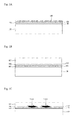
- FIGs. 1A to 1H are views illustrating a method of fabricating a light emitting device in accordance with one embodiment of the present invention
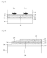
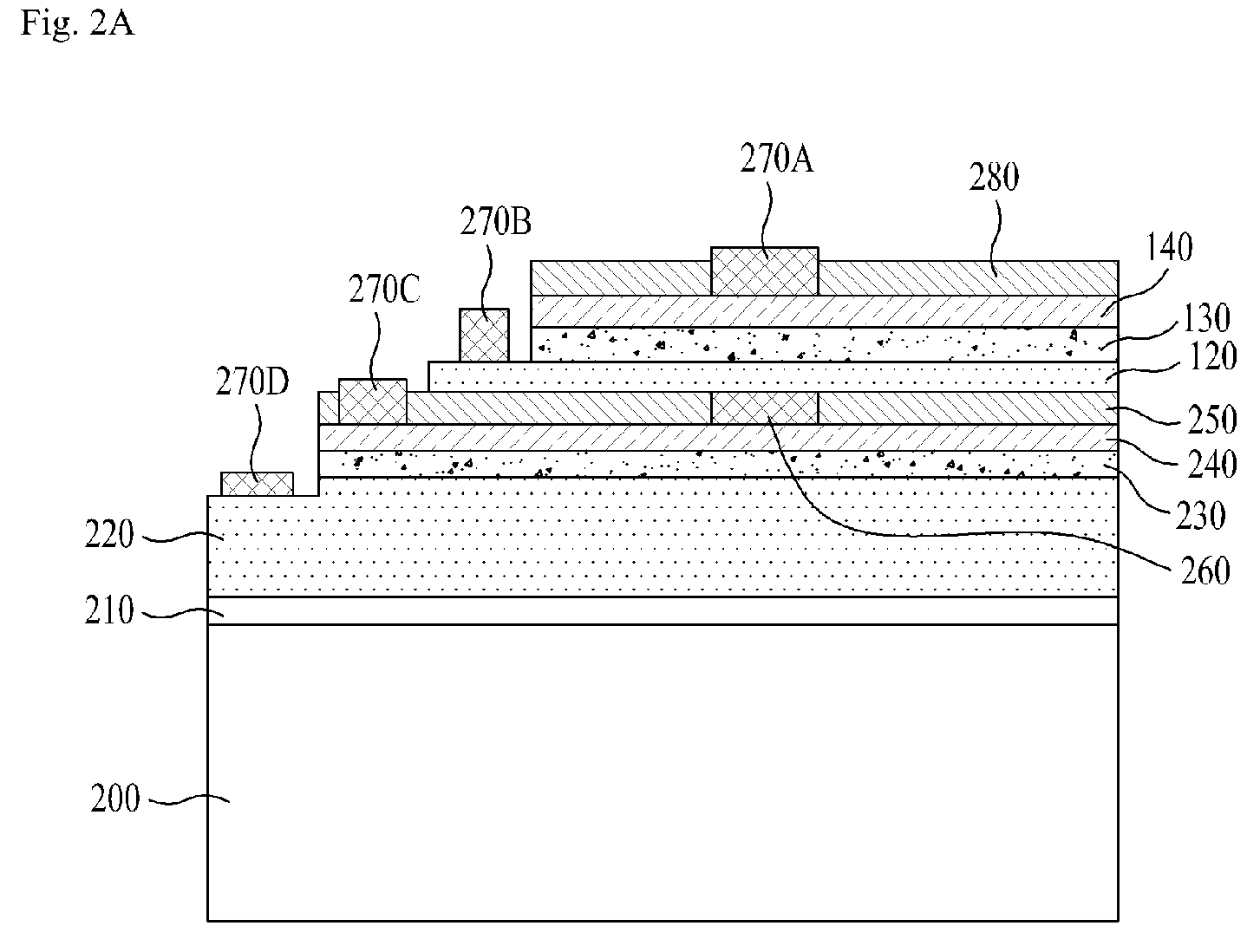
- FIGs. 2A and 2B are views illustrating a light emitting device in accordance with one embodiment of the present invention.
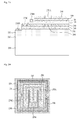
- FIGs. 3A and 3B are views illustrating a light emitting device in accordance with another embodiment of the present invention.
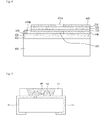
- FIG. 4 is a view illustrating a light emitting device in accordance with yet another embodiment of the present invention.
- FIG. 5 is a view illustrating a light emitting device package in accordance with one embodiment of the present invention.
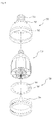
- FIG. 6 is an exploded perspective view of a lighting apparatus including light emitting device packages in accordance with one embodiment of the present invention.
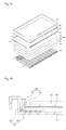
- FIGs. 7A and 7B are views illustrating a backlight including light emitting device packages in accordance with one embodiment of the present invention.
- FIGs. 1A to 1H are views illustrating a method of fabricating a light emitting device in accordance with one embodiment of the present invention. Hereinafter, the method of fabricating a light emitting device will be described with reference to FIG. 1A to 1H .
- a first nitride semiconductor is formed on a substrate 100.
- the first nitride semiconductor may include a first conductivity-type semiconductor layer 120, an active layer 130 and a second conductivity-type semiconductor layer 140.
- the active layer 130 disposed between the first conductivity-type semiconductor layer 120 and the second conductivity-type semiconductor layer 140.
- a sapphire (Al 2 O 3 ) substrate a silicon carbide (SiC) substrate, a silicon (Si) substrate, or a gallium arsenide (GaAs) substrate may be used.
- a sapphire (Al 2 O 3 ) substrate is used as the support substrate 100.
- a buffer layer 110 serves to reduce lattice mismatch and differences in coefficients of thermal expansion between the support substrate 100 and the nitride semiconductor material.
- the buffer layer 110 may be formed of at least one selected from among the group consisting of GaN, AlN, InN, InGaN, AlGaN, InAlGaN and AlInN.
- the buffer layer 110, the first conductivity-type semiconductor layer 120, the active layer 130 and the second conductivity-type semiconductor layer 140 may be formed through metal organic chemical vapor deposition (MOCVD), chemical vapor deposition (CVD), plasma-enhanced chemical vapor deposition (PECVD), molecular beam epitaxy (MBE), and hydride vapor phase epitaxy (HVPE), but formation thereof is not limited thereto.
- MOCVD metal organic chemical vapor deposition
- CVD chemical vapor deposition
- PECVD plasma-enhanced chemical vapor deposition
- MBE molecular beam epitaxy
- HVPE hydride vapor phase epitaxy
- first conductivity-type semiconductor layer 120, the active layer 130 and the second conductivity-type semiconductor layer 140 may be formed at a temperature of 700 ⁇ 1,100°C.
- the first conductivity-type semiconductor layer 120 may include a group III-V compound semiconductor doped with a first conductivity-type dopant. If the first conductivity-type semiconductor layer 120 is an N-type semiconductor layer, the first conductivity-type dopant is an N-type dopant, and the N-type dopant may include Si, Ge, Sn, Se and Te, but is not limited thereto.
- the first conductivity-type semiconductor layer 120 may include an N-doped semiconductor material having a composition formula of Al x InyGa 1-x-y N (0 ⁇ x ⁇ 1, 0 ⁇ y ⁇ 1, 0 ⁇ x+y ⁇ 1).
- the first conductivity-type semiconductor layer 120 may include at least one selected from among the group consisting of GaN, InN, AIN, InGaN, AlGaN, InAlGaN, AlInN, AlGaAs, InGaAs, AlInGaAs, GaP, AlGaP, InGaP, AlInGaP and InP.
- the first conductivity-type semiconductor layer 120 may be formed by injecting silane (SiH 4 ) gas including an N-type impurity, such as trimethyl gallium (TMGa) gas, ammonia (NH 3 ) gas, nitrogen (N 2 ) gas or silicon (Si), into a chamber.
- silane (SiH 4 ) gas including an N-type impurity such as trimethyl gallium (TMGa) gas, ammonia (NH 3 ) gas, nitrogen (N 2 ) gas or silicon (Si)
- TMGa trimethyl gallium
- NH 3 ammonia
- N 2 nitrogen
- Si silicon
- the active layer 130 emits light having energy decided by an inherent energy band of an active layer (light emitting) layer due to contact between carriers injected through the first conductivity-type semiconductor layer 120 and the second conductivity-type semiconductor layer 140.
- the active layer 130 may be formed to have at least one selected from among the group consisting of a single quantum well structure, a multi-quantum well structure (MQW), a quantum-wire structure and a quantum dot structure.
- MQW multi-quantum well structure
- the active layer 130 may be formed to have an MQW structure by injecting trimethyl gallium (TMGa) gas, ammonia (NH 3 ) gas, nitrogen (N 2 ) gas or trimethyl indium (TMIn) gas, but is not limited thereto.
- TMGa trimethyl gallium
- NH 3 ammonia
- N 2 nitrogen
- TMIn trimethyl indium
- Well/barrier layers of the active layer 130 may be formed to have at least one paired structure selected from among the group consisting of InGaN/GaN, InGaN/InGaN, GaN/AlGaN, InAlGaN/GaN, GaAs(InGaAs)/AlGaAs and GaP(InGaP)/AlGaP, but are not limited thereto.
- the well layer may be formed of a material having a lower band gap than the band gap of the barrier layer.
- the second conductivity-type semiconductor layer 140 may include a group III-V compound semiconductor doped with a second conductivity-type dopant, for example, a semiconductor material having a composition formula of In x Al y Ga 1-x-y N (0 ⁇ x ⁇ 1, 0 ⁇ y ⁇ 1, 0 ⁇ x+y ⁇ 1). If the second conductivity-type semiconductor layer 140 is a P-type semiconductor layer, the second conductivity-type dopant is a P-type dopant, and the P-type dopant may include Mg, Zn, Ca, Sr and Ba.
- the second conductivity-type semiconductor layer 140 may be a P-type GaN layer formed by injecting biscetyl cyclo pentadienyl magnesium ((EtCp 2 Mg) ⁇ Mg(C 2 H 5 C 5 H 4 ) 2 ⁇ ) including a P-type impurity, such as trimethyl gallium (TMGa) gas, ammonia (NH 3 ) gas, nitrogen (N 2 ) gas or magnesium (Mg), into a chamber, but is not limited thereto.
- TMGa trimethyl gallium
- NH 3 ammonia
- N 2 nitrogen
- Mg magnesium
- the first conductivity-type semiconductor layer 120 may be a P-type semiconductor layer and the second conductivity-type semiconductor layer 140 may be an N-type semiconductor layer.
- a semiconductor layer having polarity opposite to the second conductivity-type semiconductor layer 140 for example, an N-type semiconductor layer (not shown) if the second conductivity-type semiconductor layer 140 is a P-type semiconductor layer, may be formed on the second conductivity-type semiconductor layer 140.
- a first substrate 150 is formed on the second conductivity-type semiconductor layer 140.
- the first substrate 150 serves to support the first nitride semiconductor after removal of the support substrate 100, which will be described later.
- the first substrate 150 may be formed of at least one metal selected from among the group consisting of silicon (Si), chrome (Cr), molybdenum (Mo), nickel (Ni), gold (Au), aluminum (A1), titanium (Ti), platinum (Pt), copper (Cu) and tungsten (W), or alloys thereof.
- the first substrate 150 may be formed to a thickness of 30-500 ⁇ m.
- the support substrate 100 and the buffer layer 110 are removed.
- the removal of the support substrate 100 may be achieved by laser lift-off (LLO) using an excimer laser, dry etching or wet etching.
- the buffer layer 110 absorbs the laser and thus separation of the support substrate 100 is carried out.
- FIG. 1D illustrates the first substrate 150 on which the second conductivity-type semiconductor layer 140, the active layer 130 and the first conductivity-type semiconductor layer 120 are stacked by removing the support substrate 100 and the buffer layer 110.
- FIG. 1E another nitride semiconductor structure is formed. That is, a second nitride semiconductor is formed on a second substrate 200.
- the second nitride semiconductor may include a first conductivity-type semiconductor layer 220, an active layer 230 and a second conductivity-type semiconductor layer 240.
- compositions and methods of forming the respective layers of the second nitride semiconductor are the same as those of the above-described first nitride semiconductor.
- connection layer 250 is formed on the second conductivity-type semiconductor layer 240 of the second nitride semiconductor.
- the connection layer 250 serves to connect the second nitride semiconductor to the first nitride semiconductor.
- a current blocking layer (CBL) 260 may be formed within the connection layer 250 by patterning. That is, in order to relieve current crowding of a light emitting device which will be fabricated, the current blocking layer 260 may be formed of a metal or an insulating material. If the current blocking layer 260 is formed of a metal, a layer of the first nitride semiconductor or the second nitride semiconductor to which current is supplied may be formed of the material forming the layer and a material having Schottky characteristics.
- the first nitride semiconductor of FIG. 1D and the second nitride semiconductor are bonded.
- the first nitride semiconductor is bonded to the second nitride semiconductor through the connection layer 250 formed on the second nitride semiconductor.
- the first substrate 150 to which the first nitride semiconductor is fixed is removed.
- the removal of the first substrate 150 may be carried out by the same method as that of the removal of the support substrate 100.
- a structure in which two nitride semiconductors are connected under the condition that the connection layer 250 is interposed therebetween may be formed by the above-described method, and, in FIG. 1H , electrodes are formed.
- the electrodes may be formed after MESA etching through reactive ion etching (RIE).
- MESA etching is performed up to parts of the second conductivity-type semiconductor layers 140 and 240 and the first conductivity-type semiconductor layers 120 and 220, thereby assuring spaces in which the electrodes will be formed.
- the first conductivity-type semiconductor layer 220 and the second conductivity-type semiconductor layer 240 of the second nitride semiconductor and the first conductivity-type semiconductor layer 120 of the first nitride semiconductor are exposed, in FIG. 1H .
- the MESA etching process needs to be performed three times. Further, the second conductivity-type semiconductor layer 140 of the first nitride semiconductor is the uppermost layer, and thus may be exposed.
- the electrodes are formed, thereby forming a light emitting device having a horizontal structure, in FIGs. 2A and 2B .
- an N-type electrode 270D is formed on the first conductivity-type semiconductor layer 220 of the second nitride semiconductor
- a P-type electrode 270C is formed on the second conductivity-type semiconductor layer 220 of the second nitride semiconductor.
- An N-type electrode 270B is formed on the first conductivity-type semiconductor layer 120 of the first nitride semiconductor, and a P-type electrode 270A is formed on the second conductivity-type semiconductor layer 140 of the first nitride semiconductor.
- a transparent electrode layer 280 may be formed on the second conductivity-type semiconductor layer 140.
- the above electrodes may be formed of at least one metal selected from among the group consisting of chrome (Cr), nickel (Ni), gold (Au), aluminum (A1), titanium (Ti) and platinum (Pt), or alloys thereof.
- the transparent electrode layer 280 may include a metal thin film or a metal oxide, and in this case, the transparent electrode layer 280 may effectively transmit light emitted from the active layer 130.
- FIG. 2B is an elevation view of the light emitting device of FIG. 2A .
- the four electrodes 270A, 270B, 270C and 270D are formed on the respective semiconductor layers.
- the above-described light emitting device may be driven by AC power.
- the electrode 270A and the electrode 270D are connected to a common electrode or terminal, and the electrode 270C and the electrode 270B are connected to another common electrode or terminal.
- FIGs. 3A and 3B are views illustrating a light emitting device in accordance with another embodiment of the present invention.
- three electrodes may be formed on a light emitting device including two nitride semiconductors. That is, after the process shown in FIG. 1G , instead of performing the MESA etching process three times, the MESA etching process is performed twice in order to expose two layers.
- an N-type electrode 270C is formed on a first conductivity-type semiconductor layer 220 of the second nitride semiconductor. Further, an N-type electrode 270B is formed on a second conductivity-type semiconductor layer 240 of the second nitride semiconductor, and a P-type electrode 270A is formed on a second conductivity-type semiconductor layer 140 of the first nitride semiconductor.
- a transparent electrode layer 280 may be formed on the second conductivity-type semiconductor layer 140. Further, compositions of the electrodes are the same as those of the former embodiment shown in FIGs. 2A and 2B .
- FIG. 3B is an elevation view of the light emitting device of FIG. 3A .
- the three electrodes 270A, 270B and 270C are formed on the respective semiconductor layers.
- the above-described light emitting device may be driven by AC power.
- the electrode 270A and the electrode 270C are connected to a common electrode or terminal, and the electrode 270B is connected to another electrode or terminal.
- each of the light emitting devices in accordance with the embodiments may be connected to two electrode terminals and be driven by AC power. That is, each of the light emitting devices may be driven by applying currents in different directions, i.e., AC currents to the two active layers having the MQW structure. Further, each of the light emitting devices in accordance with the embodiments includes the two active layers having the MQW structure, and thus light/energy emitted from each of the light emitting devices may be increased.
- FIG. 4 is a view illustrating a light emitting device in accordance with yet another embodiment of the present invention.
- a first nitride semiconductor including a first conductivity-type semiconductor layer 410, an active layer 420 and a second conductivity-type semiconductor layer 430 is formed on a conductive substrate 400, and a current blocking layer 450 and a connection layer 440 are formed on the second conductivity-type semiconductor layer 430.
- the first nitride semiconductor is connected to a second nitride semiconductor including a first conductivity-type semiconductor layer 510, an active layer 520 and a second conductivity-type semiconductor layer 530 through the connection layer 440.
- a transparent electrode layer 460 may be formed on the second conductivity-type semiconductor layer 530.
- Compositions of the respective layers are the same as those of the former embodiments.
- the conductive substrate 400 may be a base substrate formed of copper (Cu), gold (Au), nickel (Ni), molybdenum (Mo), copper-tungsten (Cu-W) and includes single or multiple layers. Further, the conductive substrate 400 may be omitted, or may be disposed in a conductive sheet type.
- the second conductivity-type semiconductor layer 430 of the first nitride semiconductor is exposed, and an electrode 470B is formed on the exposed second conductivity-type semiconductor layer 430.
- the electrode 470A and the conductive substrate 400 may be connected to a common electrode or terminal, and the electrode 470B may be connected to another electrode or terminal.
- the light emitting device in accordance with the embodiment of FIG. 4 may be connected to two electrode terminals and be driven by AC power. Further, the light emitting device in accordance with the embodiment of FIG. 4 includes the two active layers having the MQW structure, and thus light/energy emitted from the light emitting device may be increased.
- FIG. 5 is a view illustrating a light emitting device package in accordance with one embodiment of the present invention.
- the light emitting device package in accordance with this embodiment will be described.
- the light emitting device package in accordance with this embodiment includes a package body 620, a first electrode layer 611 and a second electrode layer 612 installed on the package body 620, a light emitting device 600 installed on the package body 620 and electrically connected to the first electrode layer 611 and the second electrode layer 612, and a filing material 640 surrounding the light emitting device 600.
- the package body 620 may be made of a material, such as silicon, a synthetic resin or a metal.
- the package body 620 includes inclined planes around the light emitting device 600, thus increasing light extraction efficiency.
- the first electrode layer 611 and the second electrode layer 612 are electrically isolated from each other, and provide power to the light emitting device 600. Further, the first electrode layer 611 and the second electrode layer 612 may serve to reflect light emitted from the light emitting device 600 to increase light efficiency, and to discharge heat generated by the light emitting device 600 to the outside.
- the light emitting device 600 may be installed on the package body 620, or be installed on the first electrode layer 611 or the second electrode layer 612.
- the light emitting device 600 may be electrically connected to the first electrode layer 611 and the second electrode layer 612 by one method out of a wire-bonding method, a flip chip-bonding method or a die-bonding method.
- the filling material 640 may surround the light emitting device 600 to protect the light emitting device 600. Further, the filling material 640 may include a phosphor, thus varying a wavelength of light emitted from the light emitting device 600.
- the above light emitting device package may include at least one light emitting device or plural light emitting devices from among the light emitting devices in accordance with the former embodiments, but is not limited thereto.
- An array of a plurality of light emitting device packages in accordance with this embodiment may be mounted on a substrate, and optical members, such as a light guide panel, a prism sheet, a diffusion sheet, etc., may be disposed on a optical path of the light emitting device packages.
- the light emitting device packages, the substrate and the optical members may function as a light unit.
- the light emitting devices or the light emitting device package in accordance with the above-described embodiments may constitute a display device, an indicating device or a lighting system, and, for example, the lighting system may include a lamp or a streetlight.
- FIG. 6 is an exploded perspective view of a lighting apparatus including light emitting device packages in accordance with one embodiment of the present invention.
- the lighting apparatus in accordance with this embodiment includes a light source 720 to project light, a housing 700 in which the light source 720 is installed, a heat dissipation unit 710 to dissipate heat generated by the light source 720, and a holder 730 to connect the light source 720 and the heat dissipation unit 710 to the housing 700.
- the housing 700 includes a socket connector 701 connected to an electrical socket (not shown) and a body 702 connected to the socket connector 701 and accommodating the light source 720.
- One air flow hole 703 may be formed through the body 702.
- a plurality of air flow holes 703 is disposed on the body 702 of the housing 700.
- One air flow hole 703 may be formed, or plural air flow holes 703 may be disposed in a radial shape, in FIG. 6 , or various other shapes.
- the light source 720 includes a plurality of light emitting device packages 704 on a substrate 705.
- the substrate 705 may have a shape which is capable of being inserted into an opening of the housing 700, and be formed of a material having high thermal conductivity so as to transfer heat to the heat dissipation unit 710, as described later.
- the holder 730 is disposed under the light source 720.
- the holder 730 may include a frame and air flow holes. Further, although not shown in FIG. 6 , optical members may be disposed under the light source 720 so as to diffuse, scatter or converge light emitted from the light emitting device packages 704 of the light source 720.
- FIGs. 7A and 7B are views illustrating a backlight including light emitting device packages in accordance with one embodiment of the present invention.
- the backlight includes a bottom cover 810, a light emitting device package module (not shown) disposed at one side of the inside of the bottom cover 810, a reflective plate 820 disposed on the front surface of the bottom cover 810, a light guide panel 830 disposed in front of the reflective plate 820 to guide light emitted from the light emitting device package module to the front part of a display device, and optical members 840 disposed in front of the light guide panel 830.
- the display device including the backlight may further include, in addition to the above components, a liquid crystal display panel 860 disposed in front of the optical members 840, a top cover 870 disposed in front of the liquid crystal display panel 860, and fixing members 850 disposed between the bottom cover 810 and the top cover 870 to fix the bottom cover 810 and the top cover 870 together.
- the light guide panel 830 serves to guide light emitted from the light emitting device package module (not shown) so as to convert the light into surface light.
- the reflective plate 820 disposed at the rear of the light guide panel 830 serves to reflect light emitted from the light emitting device package module (not shown) toward the light guide panel 830 so as to improve light efficiency.
- the reflective plate 820 may be disposed as a separate component, in FIGs. 7A and 7B , or be disposed by coating the rear surface of the light guide panel 830 or the front surface of the bottom cover 810 with a material having high reflectivity.
- the reflective plate 820 may be formed of a material having high reflectivity and usable as an ultra-thin type, such as polyethylene terephthalate (PET).
- PET polyethylene terephthalate
- the light guide panel 830 scatters light emitted from the light emitting device package module so as to uniformly distribute the light throughout the entirety of a screen of the liquid crystal display device. Therefore, the light guide panel 830 is formed of a material having a high index of refraction and high transmittance, such as polymethylmethacrylate (PMMA), polycarbonate (PC) or polyethylene (PE).
- PMMA polymethylmethacrylate
- PC polycarbonate
- PE polyethylene
- the optical members 840 disposed on the light guide panel 830 diffuse light emitted from the light guide panel 830 by a designated angle.
- the optical members 840 enable light guided by the light guide panel 830 to be uniformly irradiated toward the liquid crystal display panel 860.
- optical sheets such as a diffusion sheet, a prism sheet and a protection sheet, may be selectively stacked, or a micro-lens array may be used.
- a plurality of optical sheets may be used, and the optical sheets may be formed of a transparent resin, such as acrylic resin, polyurethane resin or silicon resin.
- the prism sheet may include a phosphor sheet, as described above.
- the liquid crystal display panel 860 may be disposed on the front surface of the optical members 840.
- the liquid crystal display panel 860 instead of the liquid crystal display panel 860, other kinds of display devices requiring a light source may be disposed.
- FIG. 7B is a cross-sectional view of a light source part of the backlight.
- the reflective plate 820 is mounted on the bottom cover 810, and the light guide panel 830 is mounted on the reflective plate 820. Thereby, the reflective plate 820 may directly contact a heat dissipation member (not shown).
- Printed circuit boards 881 to which light emitting device packages 882 are fixed may be bonded to a bracket 812.
- the bracket 812 may be formed of a material having high thermal conductivity so as to discharge heat as well as to fix the light emitting device packages 882, and, although not shown in the drawings, heat pads may be disposed between the bracket 812 and the light emitting device packages 882 so as to facilitate heat transfer.
- bracket 812 is disposed in an L shape, in FIG. 7B , a horizontal part 812a of the bracket 812 is supported by the bottom cover 810, and a vertical part 812a of the bracket 812 fixes the printed circuit boards 881.
- a light emitting device, a method of fabricating the same and a light emitting device package in accordance with one embodiment of the present invention may be driven using AC power.
Landscapes
- Led Devices (AREA)
Abstract
Description
- The present invention relates to a light emitting device, a method of fabricating the same and a light emitting device package.
- Light emitting devices, such as light emitting diodes or laser diodes using group III-V or II-VI compound semiconductor materials, produce light of various colors, such as red, green, blue, and ultraviolet light, due to development of thin film growth techniques and element materials, and produce white light using fluorescent materials or through color mixing. Further, the light emitting devices have advantages, such as low power consumption, semi-permanent lifespan, rapid response speed, safety, and environmentally friendliness as compared to conventional light sources, such as fluorescent lamps and incandescent lamps.
- Therefore, these light emitting devices are increasingly applied to transmission modules of optical communication units, light emitting diode backlights replacing cold cathode fluorescent lamps (CCFLs) constituting backlights of liquid crystal display (LCD) devices, lighting apparatuses using white light emitting diodes replacing fluorescent lamps or incandescent lamps, headlights for vehicles and traffic lights.
- Accordingly, the present invention is directed to a light emitting device, a method of fabricating the same and a light emitting device package.
- An object of the present invention is to provide a light emitting device which is driven and emits light using AC power.
- Additional advantages, objects, and features of the embodiment will be set forth in part in the description which follows and in part will become apparent to those having ordinary skill in the art upon examination of the following or may be learned from practice of the embodiment. The objectives and other advantages of the embodiment may be realized and attained by the structure particularly pointed out in the written description and claims hereof as well as the appended drawings.
- To achieve this object and other advantages and in accordance with the purpose of the invention, as embodied and broadly described herein, a light emitting device includes a first nitride semiconductor and a second nitride semiconductor, each of which includes a first conductivity-type semiconductor layer, a second conductivity-type semiconductor layer and an active layer disposed between the first conductivity-type semiconductor layer and the second conductivity-type semiconductor layer, and a connection layer formed between the second conductivity-type semiconductor layer of the second nitride semiconductor and the first conductivity-type semiconductor layer of the first nitride semiconductor, wherein the first nitride semiconductor and the second nitride semiconductor are connected by the connection layer, and the light emitting device further comprises electrodes formed on at least a part of the second conductivity-type semiconductor layer of the first nitride semiconductor, at least a part of the first conductivity-type semiconductor layer of the second nitride semiconductor, and at least a part of the second conductivity-type semiconductor layer of the second nitride semiconductor.
- In another aspect of the present invention, a light emitting device package includes a package body, a first electrode layer and a second electrode layer disposed on the package body and electrically isolated from each other, and a light emitting device electrically connected to the first electrode layer and the second electrode layer, wherein the light emitting device includes a first nitride semiconductor and a second nitride semiconductor, each of which includes a first conductivity-type semiconductor layer, a second conductivity-type semiconductor layer and an active layer disposed between the first conductivity-type semiconductor layer and the second conductivity-type semiconductor layer, and a connection layer formed between the second conductivity-type semiconductor layer of the second nitride semiconductor and the first conductivity-type semiconductor layer of the first nitride semiconductor, wherein the first nitride semiconductor and the second nitride semiconductor are connected by the connection layer, and the light emitting device package further comprises electrodes formed on at least a part of the second conductivity-type semiconductor layer of the first nitride semiconductor, at least a part of the first conductivity-type semiconductor layer of the second nitride semiconductor, and at least a part of the second conductivity-type semiconductor layer of the second nitride semiconductor.
- In another aspect of the present invention, a lighting system includes light emitting device packages, each of which includes at least one light emitting device, a circuit board electrically connected to the light emitting device packages, a substrate to support the light emitting device packages and the circuit board, and optical members to transmit light emitted from the light emitting device packages, wherein the at least one light emitting device includes a first nitride semiconductor and a second nitride semiconductor, each of which includes a first conductivity-type semiconductor layer, a second conductivity-type semiconductor layer and an active layer disposed between the first conductivity-type semiconductor layer and the second conductivity-type semiconductor layer, and a connection layer formed between the second conductivity-type semiconductor layer of the second nitride semiconductor and the first conductivity-type semiconductor layer of the first nitride semiconductor, wherein the first nitride semiconductor and the second nitride semiconductor are connected by the connection layer, and the lighting system further comprises electrodes formed on at least a part of the second conductivity-type semiconductor layer of the first nitride semiconductor, at least a part of the first conductivity-type semiconductor layer of the second nitride semiconductor, and at least a part of the second conductivity-type semiconductor layer of the second nitride semiconductor.
- It is to be understood that both the foregoing general description and the following detailed description of the present invention are exemplary and explanatory and are intended to provide further explanation of the embodiment as claimed.
- The accompanying drawings, which are included to provide a further understanding of the disclosure and are incorporated in and constitute a part of this application, illustrate embodiment(s) of the disclosure and together with the description serve to explain the principle of the disclosure. In the drawings:
-
FIGs. 1A to 1H are views illustrating a method of fabricating a light emitting device in accordance with one embodiment of the present invention; -
FIGs. 2A and 2B are views illustrating a light emitting device in accordance with one embodiment of the present invention; -
FIGs. 3A and 3B are views illustrating a light emitting device in accordance with another embodiment of the present invention; -
FIG. 4 is a view illustrating a light emitting device in accordance with yet another embodiment of the present invention; -
FIG. 5 is a view illustrating a light emitting device package in accordance with one embodiment of the present invention; -
FIG. 6 is an exploded perspective view of a lighting apparatus including light emitting device packages in accordance with one embodiment of the present invention; and -
FIGs. 7A and 7B are views illustrating a backlight including light emitting device packages in accordance with one embodiment of the present invention. - Hereinafter, a light emitting device, a method of fabricating the same and a light emitting device package in accordance with embodiments of the present invention will be described with reference to the accompanying drawings.
- It will be understood that when an element is referred to as being 'on' or 'under' another element, it can be directly on/under the element, and one or more intervening elements may also be present. When an element is referred to as being 'on' or 'under', 'under the element' as well as 'on the element' can be included based on the element.
- In the drawings, the thicknesses or sizes of respective layers are exaggerated, omitted, or schematically illustrated for convenience and clarity of description. Further, the sizes of the respective elements do not denote the actual sizes thereof.
-
FIGs. 1A to 1H are views illustrating a method of fabricating a light emitting device in accordance with one embodiment of the present invention. Hereinafter, the method of fabricating a light emitting device will be described with reference toFIG. 1A to 1H . - First, in
FIG. 1A , a first nitride semiconductor is formed on asubstrate 100. Here, the first nitride semiconductor may include a first conductivity-type semiconductor layer 120, anactive layer 130 and a second conductivity-type semiconductor layer 140. Theactive layer 130 disposed between the first conductivity-type semiconductor layer 120 and the second conductivity-type semiconductor layer 140. - For example, as the
support substrate 100, a sapphire (Al2O3) substrate, a silicon carbide (SiC) substrate, a silicon (Si) substrate, or a gallium arsenide (GaAs) substrate may be used. Preferably, as thesupport substrate 100, a sapphire (Al2O3) substrate is used. - A
buffer layer 110 serves to reduce lattice mismatch and differences in coefficients of thermal expansion between thesupport substrate 100 and the nitride semiconductor material. For example, thebuffer layer 110 may be formed of at least one selected from among the group consisting of GaN, AlN, InN, InGaN, AlGaN, InAlGaN and AlInN. - The
buffer layer 110, the first conductivity-type semiconductor layer 120, theactive layer 130 and the second conductivity-type semiconductor layer 140 may be formed through metal organic chemical vapor deposition (MOCVD), chemical vapor deposition (CVD), plasma-enhanced chemical vapor deposition (PECVD), molecular beam epitaxy (MBE), and hydride vapor phase epitaxy (HVPE), but formation thereof is not limited thereto. - Further, the first conductivity-
type semiconductor layer 120, theactive layer 130 and the second conductivity-type semiconductor layer 140 may be formed at a temperature of 700∼1,100°C. - The first conductivity-
type semiconductor layer 120 may include a group III-V compound semiconductor doped with a first conductivity-type dopant. If the first conductivity-type semiconductor layer 120 is an N-type semiconductor layer, the first conductivity-type dopant is an N-type dopant, and the N-type dopant may include Si, Ge, Sn, Se and Te, but is not limited thereto. - The first conductivity-
type semiconductor layer 120 may include an N-doped semiconductor material having a composition formula of AlxInyGa1-x-yN (0≤x≤1, 0≤y≤1, 0≤x+y≤1). For example, the first conductivity-type semiconductor layer 120 may include at least one selected from among the group consisting of GaN, InN, AIN, InGaN, AlGaN, InAlGaN, AlInN, AlGaAs, InGaAs, AlInGaAs, GaP, AlGaP, InGaP, AlInGaP and InP. - The first conductivity-
type semiconductor layer 120 may be formed by injecting silane (SiH4) gas including an N-type impurity, such as trimethyl gallium (TMGa) gas, ammonia (NH3) gas, nitrogen (N2) gas or silicon (Si), into a chamber. - The
active layer 130 emits light having energy decided by an inherent energy band of an active layer (light emitting) layer due to contact between carriers injected through the first conductivity-type semiconductor layer 120 and the second conductivity-type semiconductor layer 140. - The
active layer 130 may be formed to have at least one selected from among the group consisting of a single quantum well structure, a multi-quantum well structure (MQW), a quantum-wire structure and a quantum dot structure. For example, theactive layer 130 may be formed to have an MQW structure by injecting trimethyl gallium (TMGa) gas, ammonia (NH3) gas, nitrogen (N2) gas or trimethyl indium (TMIn) gas, but is not limited thereto. - Well/barrier layers of the
active layer 130 may be formed to have at least one paired structure selected from among the group consisting of InGaN/GaN, InGaN/InGaN, GaN/AlGaN, InAlGaN/GaN, GaAs(InGaAs)/AlGaAs and GaP(InGaP)/AlGaP, but are not limited thereto. The well layer may be formed of a material having a lower band gap than the band gap of the barrier layer. - The second conductivity-
type semiconductor layer 140 may include a group III-V compound semiconductor doped with a second conductivity-type dopant, for example, a semiconductor material having a composition formula of InxAlyGa1-x-yN (0≤x≤1, 0≤y≤1, 0≤x+y≤1). If the second conductivity-type semiconductor layer 140 is a P-type semiconductor layer, the second conductivity-type dopant is a P-type dopant, and the P-type dopant may include Mg, Zn, Ca, Sr and Ba. - The second conductivity-
type semiconductor layer 140 may be a P-type GaN layer formed by injecting biscetyl cyclo pentadienyl magnesium ((EtCp2Mg){Mg(C2H5C5H4)2}) including a P-type impurity, such as trimethyl gallium (TMGa) gas, ammonia (NH3) gas, nitrogen (N2) gas or magnesium (Mg), into a chamber, but is not limited thereto. - In this embodiment, the first conductivity-
type semiconductor layer 120 may be a P-type semiconductor layer and the second conductivity-type semiconductor layer 140 may be an N-type semiconductor layer. Further, a semiconductor layer having polarity opposite to the second conductivity-type semiconductor layer 140, for example, an N-type semiconductor layer (not shown) if the second conductivity-type semiconductor layer 140 is a P-type semiconductor layer, may be formed on the second conductivity-type semiconductor layer 140. - Thereafter, in
FIG. 1B , afirst substrate 150 is formed on the second conductivity-type semiconductor layer 140. Here, thefirst substrate 150 serves to support the first nitride semiconductor after removal of thesupport substrate 100, which will be described later. If thefirst substrate 150 is formed of a conductive material, thefirst substrate 150 may be formed of at least one metal selected from among the group consisting of silicon (Si), chrome (Cr), molybdenum (Mo), nickel (Ni), gold (Au), aluminum (A1), titanium (Ti), platinum (Pt), copper (Cu) and tungsten (W), or alloys thereof. - Further, the
first substrate 150 may be formed to a thickness of 30-500 µm. - Thereafter, in
FIG. 1C , thesupport substrate 100 and thebuffer layer 110 are removed. Here, the removal of thesupport substrate 100 may be achieved by laser lift-off (LLO) using an excimer laser, dry etching or wet etching. - Here, if the removal of the
support substrate 100 is achieved by LLO, when a laser having energy smaller than the energy band gap of thesupport substrate 100 and greater than the energy band gap of the first conductivity-type semiconductor layer 120 is irradiated, thebuffer layer 110 absorbs the laser and thus separation of thesupport substrate 100 is carried out. -
FIG. 1D illustrates thefirst substrate 150 on which the second conductivity-type semiconductor layer 140, theactive layer 130 and the first conductivity-type semiconductor layer 120 are stacked by removing thesupport substrate 100 and thebuffer layer 110. - Thereafter, in
FIG. 1E , another nitride semiconductor structure is formed. That is, a second nitride semiconductor is formed on asecond substrate 200. Here, the second nitride semiconductor may include a first conductivity-type semiconductor layer 220, anactive layer 230 and a second conductivity-type semiconductor layer 240. - Compositions and methods of forming the respective layers of the second nitride semiconductor are the same as those of the above-described first nitride semiconductor.
- Thereafter, a
connection layer 250 is formed on the second conductivity-type semiconductor layer 240 of the second nitride semiconductor. Theconnection layer 250 serves to connect the second nitride semiconductor to the first nitride semiconductor. - Further, a current blocking layer (CBL) 260 may be formed within the
connection layer 250 by patterning. That is, in order to relieve current crowding of a light emitting device which will be fabricated, thecurrent blocking layer 260 may be formed of a metal or an insulating material. If thecurrent blocking layer 260 is formed of a metal, a layer of the first nitride semiconductor or the second nitride semiconductor to which current is supplied may be formed of the material forming the layer and a material having Schottky characteristics. - Thereafter, in FIG. IF, the first nitride semiconductor of
FIG. 1D and the second nitride semiconductor are bonded. Here, the first nitride semiconductor is bonded to the second nitride semiconductor through theconnection layer 250 formed on the second nitride semiconductor. - Thereafter, in
FIG. 1G , thefirst substrate 150 to which the first nitride semiconductor is fixed is removed. Here, the removal of thefirst substrate 150 may be carried out by the same method as that of the removal of thesupport substrate 100. - A structure in which two nitride semiconductors are connected under the condition that the
connection layer 250 is interposed therebetween may be formed by the above-described method, and, inFIG. 1H , electrodes are formed. Here, the electrodes may be formed after MESA etching through reactive ion etching (RIE). - That is, MESA etching is performed up to parts of the second conductivity-type semiconductor layers 140 and 240 and the first conductivity-type semiconductor layers 120 and 220, thereby assuring spaces in which the electrodes will be formed.
- When the MESA etching process has been completed, the first conductivity-
type semiconductor layer 220 and the second conductivity-type semiconductor layer 240 of the second nitride semiconductor and the first conductivity-type semiconductor layer 120 of the first nitride semiconductor are exposed, inFIG. 1H . - Here, in order to expose the above three layers, the MESA etching process needs to be performed three times. Further, the second conductivity-
type semiconductor layer 140 of the first nitride semiconductor is the uppermost layer, and thus may be exposed. - After the MESA etching process has been completed, the electrodes are formed, thereby forming a light emitting device having a horizontal structure, in
FIGs. 2A and 2B . - In
FIG. 2A , an N-type electrode 270D is formed on the first conductivity-type semiconductor layer 220 of the second nitride semiconductor, and a P-type electrode 270C is formed on the second conductivity-type semiconductor layer 220 of the second nitride semiconductor. - An N-
type electrode 270B is formed on the first conductivity-type semiconductor layer 120 of the first nitride semiconductor, and a P-type electrode 270A is formed on the second conductivity-type semiconductor layer 140 of the first nitride semiconductor. Here, atransparent electrode layer 280 may be formed on the second conductivity-type semiconductor layer 140. - The above electrodes may be formed of at least one metal selected from among the group consisting of chrome (Cr), nickel (Ni), gold (Au), aluminum (A1), titanium (Ti) and platinum (Pt), or alloys thereof.
- Further, the
transparent electrode layer 280 may include a metal thin film or a metal oxide, and in this case, thetransparent electrode layer 280 may effectively transmit light emitted from theactive layer 130. -
FIG. 2B is an elevation view of the light emitting device ofFIG. 2A . InFIG. 2B , the fourelectrodes - The above-described light emitting device may be driven by AC power. Here, the
electrode 270A and theelectrode 270D are connected to a common electrode or terminal, and theelectrode 270C and theelectrode 270B are connected to another common electrode or terminal. -
FIGs. 3A and 3B are views illustrating a light emitting device in accordance with another embodiment of the present invention. - With reference to
FIGs. 3A and 3B , three electrodes may be formed on a light emitting device including two nitride semiconductors. That is, after the process shown inFIG. 1G , instead of performing the MESA etching process three times, the MESA etching process is performed twice in order to expose two layers. - In
FIG. 3A , an N-type electrode 270C is formed on a first conductivity-type semiconductor layer 220 of the second nitride semiconductor. Further, an N-type electrode 270B is formed on a second conductivity-type semiconductor layer 240 of the second nitride semiconductor, and a P-type electrode 270A is formed on a second conductivity-type semiconductor layer 140 of the first nitride semiconductor. - In the same manner as the former embodiment shown in
FIGs. 2A and 2B , atransparent electrode layer 280 may be formed on the second conductivity-type semiconductor layer 140. Further, compositions of the electrodes are the same as those of the former embodiment shown inFIGs. 2A and 2B . -
FIG. 3B is an elevation view of the light emitting device ofFIG. 3A . InFIG. 3B , the threeelectrodes - Further, the above-described light emitting device may be driven by AC power. Here, the
electrode 270A and theelectrode 270C are connected to a common electrode or terminal, and theelectrode 270B is connected to another electrode or terminal. - The above-described light emitting devices in accordance with the embodiments may be connected to two electrode terminals and be driven by AC power. That is, each of the light emitting devices may be driven by applying currents in different directions, i.e., AC currents to the two active layers having the MQW structure. Further, each of the light emitting devices in accordance with the embodiments includes the two active layers having the MQW structure, and thus light/energy emitted from each of the light emitting devices may be increased.
-
FIG. 4 is a view illustrating a light emitting device in accordance with yet another embodiment of the present invention. - With reference to
FIG. 4 , a first nitride semiconductor including a first conductivity-type semiconductor layer 410, anactive layer 420 and a second conductivity-type semiconductor layer 430 is formed on aconductive substrate 400, and acurrent blocking layer 450 and aconnection layer 440 are formed on the second conductivity-type semiconductor layer 430. - The first nitride semiconductor is connected to a second nitride semiconductor including a first conductivity-
type semiconductor layer 510, anactive layer 520 and a second conductivity-type semiconductor layer 530 through theconnection layer 440. - Further, a
transparent electrode layer 460 may be formed on the second conductivity-type semiconductor layer 530. Compositions of the respective layers are the same as those of the former embodiments. - The
conductive substrate 400 may be a base substrate formed of copper (Cu), gold (Au), nickel (Ni), molybdenum (Mo), copper-tungsten (Cu-W) and includes single or multiple layers. Further, theconductive substrate 400 may be omitted, or may be disposed in a conductive sheet type. - Further, removal of a support substrate on which the second nitride semiconductor is stacked by Laser Lift-Off is the same as in the former embodiments.
- In this embodiment shown in
FIG. 4 , by performing the MESA etching process once, the second conductivity-type semiconductor layer 430 of the first nitride semiconductor is exposed, and anelectrode 470B is formed on the exposed second conductivity-type semiconductor layer 430. - Then, power is connected to two
electrodes conductive substrate 400. Theelectrode 470A and theconductive substrate 400 may be connected to a common electrode or terminal, and theelectrode 470B may be connected to another electrode or terminal. - Therefore, the light emitting device in accordance with the embodiment of
FIG. 4 may be connected to two electrode terminals and be driven by AC power. Further, the light emitting device in accordance with the embodiment ofFIG. 4 includes the two active layers having the MQW structure, and thus light/energy emitted from the light emitting device may be increased. -
FIG. 5 is a view illustrating a light emitting device package in accordance with one embodiment of the present invention. Hereinafter, with reference toFIG. 5 , the light emitting device package in accordance with this embodiment will be described. - In
FIG. 5 , the light emitting device package in accordance with this embodiment includes a package body 620, afirst electrode layer 611 and asecond electrode layer 612 installed on the package body 620, a light emitting device 600 installed on the package body 620 and electrically connected to thefirst electrode layer 611 and thesecond electrode layer 612, and afiling material 640 surrounding the light emitting device 600. - The package body 620 may be made of a material, such as silicon, a synthetic resin or a metal. The package body 620 includes inclined planes around the light emitting device 600, thus increasing light extraction efficiency.
- The
first electrode layer 611 and thesecond electrode layer 612 are electrically isolated from each other, and provide power to the light emitting device 600. Further, thefirst electrode layer 611 and thesecond electrode layer 612 may serve to reflect light emitted from the light emitting device 600 to increase light efficiency, and to discharge heat generated by the light emitting device 600 to the outside. - The light emitting device 600 may be installed on the package body 620, or be installed on the
first electrode layer 611 or thesecond electrode layer 612. - The light emitting device 600 may be electrically connected to the
first electrode layer 611 and thesecond electrode layer 612 by one method out of a wire-bonding method, a flip chip-bonding method or a die-bonding method. - The filling
material 640 may surround the light emitting device 600 to protect the light emitting device 600. Further, the fillingmaterial 640 may include a phosphor, thus varying a wavelength of light emitted from the light emitting device 600. - The above light emitting device package may include at least one light emitting device or plural light emitting devices from among the light emitting devices in accordance with the former embodiments, but is not limited thereto.
- An array of a plurality of light emitting device packages in accordance with this embodiment may be mounted on a substrate, and optical members, such as a light guide panel, a prism sheet, a diffusion sheet, etc., may be disposed on a optical path of the light emitting device packages. The light emitting device packages, the substrate and the optical members may function as a light unit. In accordance with another embodiment, the light emitting devices or the light emitting device package in accordance with the above-described embodiments may constitute a display device, an indicating device or a lighting system, and, for example, the lighting system may include a lamp or a streetlight.
-
FIG. 6 is an exploded perspective view of a lighting apparatus including light emitting device packages in accordance with one embodiment of the present invention. - The lighting apparatus in accordance with this embodiment includes a
light source 720 to project light, ahousing 700 in which thelight source 720 is installed, aheat dissipation unit 710 to dissipate heat generated by thelight source 720, and aholder 730 to connect thelight source 720 and theheat dissipation unit 710 to thehousing 700. - The
housing 700 includes asocket connector 701 connected to an electrical socket (not shown) and abody 702 connected to thesocket connector 701 and accommodating thelight source 720. Oneair flow hole 703 may be formed through thebody 702. - In this embodiment, a plurality of air flow holes 703 is disposed on the
body 702 of thehousing 700. Oneair flow hole 703 may be formed, or plural air flow holes 703 may be disposed in a radial shape, inFIG. 6 , or various other shapes. - The
light source 720 includes a plurality of light emitting device packages 704 on asubstrate 705. Here, thesubstrate 705 may have a shape which is capable of being inserted into an opening of thehousing 700, and be formed of a material having high thermal conductivity so as to transfer heat to theheat dissipation unit 710, as described later. - The
holder 730 is disposed under thelight source 720. Theholder 730 may include a frame and air flow holes. Further, although not shown inFIG. 6 , optical members may be disposed under thelight source 720 so as to diffuse, scatter or converge light emitted from the light emitting device packages 704 of thelight source 720. -
FIGs. 7A and 7B are views illustrating a backlight including light emitting device packages in accordance with one embodiment of the present invention. - In
FIGs. 7A and 7B , the backlight includes a bottom cover 810, a light emitting device package module (not shown) disposed at one side of the inside of the bottom cover 810, a reflective plate 820 disposed on the front surface of the bottom cover 810, alight guide panel 830 disposed in front of the reflective plate 820 to guide light emitted from the light emitting device package module to the front part of a display device, and optical members 840 disposed in front of thelight guide panel 830. The display device including the backlight may further include, in addition to the above components, a liquid crystal display panel 860 disposed in front of the optical members 840, a top cover 870 disposed in front of the liquid crystal display panel 860, and fixing members 850 disposed between the bottom cover 810 and the top cover 870 to fix the bottom cover 810 and the top cover 870 together. - The
light guide panel 830 serves to guide light emitted from the light emitting device package module (not shown) so as to convert the light into surface light. The reflective plate 820 disposed at the rear of thelight guide panel 830 serves to reflect light emitted from the light emitting device package module (not shown) toward thelight guide panel 830 so as to improve light efficiency. - The reflective plate 820 may be disposed as a separate component, in
FIGs. 7A and 7B , or be disposed by coating the rear surface of thelight guide panel 830 or the front surface of the bottom cover 810 with a material having high reflectivity. - Here, the reflective plate 820 may be formed of a material having high reflectivity and usable as an ultra-thin type, such as polyethylene terephthalate (PET).
- Further, the
light guide panel 830 scatters light emitted from the light emitting device package module so as to uniformly distribute the light throughout the entirety of a screen of the liquid crystal display device. Therefore, thelight guide panel 830 is formed of a material having a high index of refraction and high transmittance, such as polymethylmethacrylate (PMMA), polycarbonate (PC) or polyethylene (PE). - The optical members 840 disposed on the
light guide panel 830 diffuse light emitted from thelight guide panel 830 by a designated angle. The optical members 840 enable light guided by thelight guide panel 830 to be uniformly irradiated toward the liquid crystal display panel 860. - As the optical members 840, optical sheets, such as a diffusion sheet, a prism sheet and a protection sheet, may be selectively stacked, or a micro-lens array may be used. Here, a plurality of optical sheets may be used, and the optical sheets may be formed of a transparent resin, such as acrylic resin, polyurethane resin or silicon resin. Further, the prism sheet may include a phosphor sheet, as described above.
- The liquid crystal display panel 860 may be disposed on the front surface of the optical members 840. Here, it will be apparent that, instead of the liquid crystal display panel 860, other kinds of display devices requiring a light source may be disposed.
-
FIG. 7B is a cross-sectional view of a light source part of the backlight. - In
FIG. 7B , the reflective plate 820 is mounted on the bottom cover 810, and thelight guide panel 830 is mounted on the reflective plate 820. Thereby, the reflective plate 820 may directly contact a heat dissipation member (not shown). - Printed circuit boards 881 to which light emitting device packages 882 are fixed may be bonded to a bracket 812. Here, the bracket 812 may be formed of a material having high thermal conductivity so as to discharge heat as well as to fix the light emitting device packages 882, and, although not shown in the drawings, heat pads may be disposed between the bracket 812 and the light emitting device packages 882 so as to facilitate heat transfer.
- Further, the bracket 812 is disposed in an L shape, in
FIG. 7B , a horizontal part 812a of the bracket 812 is supported by the bottom cover 810, and a vertical part 812a of the bracket 812 fixes the printed circuit boards 881. - As apparent from the above description, a light emitting device, a method of fabricating the same and a light emitting device package in accordance with one embodiment of the present invention may be driven using AC power.
- It will be apparent to those skilled in the art that various modifications and variations can be made in the present invention without departing from the spirit or scope of the invention. Thus, it is intended that the present invention covers the modifications and variations of this invention provided they come within the scope of the appended claims and their equivalents.
Claims (15)
- A light emitting device comprising:a first nitride semiconductor and a second nitride semiconductor, each of which includes a first conductivity-type semiconductor layer, a second conductivity-type semiconductor layer and an active layer disposed between the first conductivity-type semiconductor layer and the second conductivity-type semiconductor layer; anda connection layer formed between the second conductivity-type semiconductor layer of the second nitride semiconductor and the first conductivity-type semiconductor layer of the first nitride semiconductor,wherein the first nitride semiconductor and the second nitride semiconductor are connected by the connection layer, and the light emitting device further comprises electrodes formed on at least a part of the second conductivity-type semiconductor layer of the first nitride semiconductor, at least a part of the first conductivity-type semiconductor layer of the second nitride semiconductor, and at least a part of the second conductivity-type semiconductor layer of the second nitride semiconductor.
- The light emitting device according to claim 1, wherein the electrode further formed on an exposed part of the first conductivity-type semiconductor layer of the first nitride semiconductor.
- The light emitting device according to claim 1, further comprising a current blocking layer formed between the second conductivity-type semiconductor layer of the second nitride semiconductor and the first conductivity-type semiconductor layer of the first nitride semiconductor.
- The light emitting device according to claim 3, wherein the current blocking layer is formed of a metal or an insulating material.
- The light emitting device according to claim 3, wherein the electrode further formed on an exposed part of the first conductivity-type semiconductor layer of the first nitride semiconductor and the current blocking layer is formed corresponding to the electrode.
- The light emitting device according to claim 3, wherein the current blocking layer is formed within the connection layer.
- The light emitting device according to claim 3, wherein the current blocking layer is formed of a metal and a material, the material having Schottky characteristics with another material, and a layer of the first nitride semiconductor or the second nitride semiconductor to which current is supplied is formed of the another material.
- The light emitting device according to claim 1, further comprising a transparent electrode layer formed on the first conductivity-type semiconductor layer of the first nitride semiconductor.
- The light emitting device according to claim 1, wherein the electrode formed on at least the part of the second conductivity-type semiconductor layer of the first nitride semiconductor and the electrode formed on at least the part of the first conductivity-type semiconductor layer of the second nitride semiconductor are connected to a first electrode.
- The light emitting device according to claim 9, wherein the electrode formed on at least the part of the second conductivity-type semiconductor layer of the second nitride semiconductor is connected to a second electrode.
- The light emitting device according to claim 2, wherein the electrode formed on the part of the first conductivity-type semiconductor layer of the first nitride semiconductor and the electrode formed on at least the part of the second conductivity-type semiconductor layer of the second nitride semiconductor are connected to a first electrode.
- The light emitting device according to claim 2, wherein the electrode formed on at least the part of the second conductivity-type semiconductor layer of the first nitride semiconductor and the electrode formed on at least the part of the first conductivity-type semiconductor layer of the second nitride semiconductor are connected to a second electrode.
- The light emitting device according to claim 1, wherein, the first conductivity-type semiconductor layer is an N-type semiconductor layer and the second conductivity-type semiconductor layer is an P-type semiconductor layer.
- A light emitting device package comprising:a package body;a first electrode layer and a second electrode layer disposed on the package body and electrically isolated from each other; anda light emitting device according to any one of claims 1 to 13, the light emitting device is electrically connected to the first electrode layer and the second electrode layer.
- A lighting system comprising:light emitting device packages, each of which includes at least one light emitting device according to any one of claims 1 to 13;a circuit board electrically connected to the light emitting device packages;a substrate to support the light emitting device packages and the circuit board; andoptical members to transmit light emitted from the light emitting device packages.
Applications Claiming Priority (1)
| Application Number | Priority Date | Filing Date | Title |
|---|---|---|---|
| KR1020100047833A KR101039609B1 (en) | 2010-05-24 | 2010-05-24 | Light emitting device, manufacturing method and light emitting device package |
Publications (3)
| Publication Number | Publication Date |
|---|---|
| EP2390916A2 true EP2390916A2 (en) | 2011-11-30 |
| EP2390916A3 EP2390916A3 (en) | 2015-06-03 |
| EP2390916B1 EP2390916B1 (en) | 2019-04-10 |
Family
ID=44405157
Family Applications (1)
| Application Number | Title | Priority Date | Filing Date |
|---|---|---|---|
| EP11167102.0A Active EP2390916B1 (en) | 2010-05-24 | 2011-05-23 | Stacked light emitting devices |
Country Status (4)
| Country | Link |
|---|---|
| US (1) | US8507944B2 (en) |
| EP (1) | EP2390916B1 (en) |
| KR (1) | KR101039609B1 (en) |
| CN (1) | CN102263180A (en) |
Families Citing this family (8)
| Publication number | Priority date | Publication date | Assignee | Title |
|---|---|---|---|---|
| TWD146468S1 (en) * | 2011-05-24 | 2012-04-11 | 隆達電子股份有限公司 | Chip |
| TWD146470S (en) * | 2011-05-24 | 2012-04-11 | 隆達電子股份有限公司 | Chip |
| TWD146471S (en) * | 2011-05-24 | 2012-04-11 | 隆達電子股份有限公司 | Chip |
| TWD146469S (en) * | 2011-05-24 | 2012-04-11 | 隆達電子股份有限公司 | Chip |
| USD656908S1 (en) * | 2011-07-05 | 2012-04-03 | Epistar Corporation | Light emitting device |
| US20130285010A1 (en) * | 2012-04-27 | 2013-10-31 | Phostek, Inc. | Stacked led device with posts in adhesive layer |
| JP5440674B1 (en) * | 2012-09-18 | 2014-03-12 | ウシオ電機株式会社 | LED element and manufacturing method thereof |
| TWI871647B (en) * | 2023-05-31 | 2025-02-01 | 隆達電子股份有限公司 | Light-emitting device and method of manufacturing the same |
Family Cites Families (13)
| Publication number | Priority date | Publication date | Assignee | Title |
|---|---|---|---|---|
| TW522534B (en) * | 2001-09-11 | 2003-03-01 | Hsiu-Hen Chang | Light source of full color LED using die bonding and packaging technology |
| KR100970611B1 (en) | 2003-12-17 | 2010-07-15 | 우리엘에스티 주식회사 | Light emitting diodes emitting a plurality of wavelengths of light and a manufacturing method thereof |
| TWI229463B (en) | 2004-02-02 | 2005-03-11 | South Epitaxy Corp | Light-emitting diode structure with electro-static discharge protection |
| US7119374B2 (en) * | 2004-02-20 | 2006-10-10 | Supernova Optoelectronics Corp. | Gallium nitride based light emitting device and the fabricating method for the same |
| US20060002442A1 (en) * | 2004-06-30 | 2006-01-05 | Kevin Haberern | Light emitting devices having current blocking structures and methods of fabricating light emitting devices having current blocking structures |
| US7474681B2 (en) | 2005-05-13 | 2009-01-06 | Industrial Technology Research Institute | Alternating current light-emitting device |
| TW200640045A (en) * | 2005-05-13 | 2006-11-16 | Ind Tech Res Inst | Alternating current light-emitting device |
| KR100691177B1 (en) * | 2005-05-31 | 2007-03-09 | 삼성전기주식회사 | White light emitting device |
| CN100388515C (en) * | 2005-09-30 | 2008-05-14 | 晶能光电(江西)有限公司 | Semiconductor light emitting device and manufacturing method thereof |
| KR100793333B1 (en) | 2006-04-21 | 2008-01-11 | 삼성전기주식회사 | Method of manufacturing surface mount light emitting diode device |
| KR20080092716A (en) | 2007-04-13 | 2008-10-16 | 삼성전자주식회사 | Organic light emitting device and organic light emitting display device including the same |
| US8124991B2 (en) * | 2007-07-26 | 2012-02-28 | The Regents Of The University Of California | Light emitting diodes with a P-type surface bonded to a transparent submount to increase light extraction efficiency |
| KR101332794B1 (en) * | 2008-08-05 | 2013-11-25 | 삼성전자주식회사 | Light emitting device, light emitting system comprising the same, and fabricating method of the light emitting device and the light emitting system |
-
2010
- 2010-05-24 KR KR1020100047833A patent/KR101039609B1/en not_active Expired - Fee Related
-
2011
- 2011-05-23 EP EP11167102.0A patent/EP2390916B1/en active Active
- 2011-05-24 US US13/114,246 patent/US8507944B2/en active Active
- 2011-05-24 CN CN2011101451777A patent/CN102263180A/en active Pending
Non-Patent Citations (1)
| Title |
|---|
| None |
Also Published As
| Publication number | Publication date |
|---|---|
| US8507944B2 (en) | 2013-08-13 |
| KR101039609B1 (en) | 2011-06-09 |
| EP2390916A3 (en) | 2015-06-03 |
| CN102263180A (en) | 2011-11-30 |
| EP2390916B1 (en) | 2019-04-10 |
| US20110284901A1 (en) | 2011-11-24 |
Similar Documents
| Publication | Publication Date | Title |
|---|---|---|
| US10141478B2 (en) | Structure of a reflective electrode and an OHMIC layer of a light emitting device | |
| US9356007B2 (en) | Light emitting device and lighting apparatus including the same | |
| EP2390916B1 (en) | Stacked light emitting devices | |
| US9673254B2 (en) | Light emitting device | |
| EP2860770B1 (en) | Light-emitting element | |
| US8536606B2 (en) | Light emitting device, light emitting device package including the same and lighting system | |
| US20110316004A1 (en) | Light emitting device | |
| EP2375457B1 (en) | Light emitting device with a monolithic re-emission layer | |
| US8212265B2 (en) | Light emitting device and method for fabricating the light emitting device | |
| KR20130139015A (en) | Light emitting device | |
| KR101861633B1 (en) | Light emitting device and light emitting device package including the same | |
| KR20130074989A (en) | Light emitting device | |
| KR20120038126A (en) | Light emitting device | |
| KR20130010673A (en) | Light emitting device package | |
| KR20120045877A (en) | Light emitting device | |
| KR20120037708A (en) | Light emitting device |
Legal Events
| Date | Code | Title | Description |
|---|---|---|---|
| AK | Designated contracting states |
Kind code of ref document: A2 Designated state(s): AL AT BE BG CH CY CZ DE DK EE ES FI FR GB GR HR HU IE IS IT LI LT LU LV MC MK MT NL NO PL PT RO RS SE SI SK SM TR |
|
| AX | Request for extension of the european patent |
Extension state: BA ME |
|
| PUAI | Public reference made under article 153(3) epc to a published international application that has entered the european phase |
Free format text: ORIGINAL CODE: 0009012 |
|
| 17P | Request for examination filed |
Effective date: 20140327 |
|
| RBV | Designated contracting states (corrected) |
Designated state(s): AL AT BE BG CH CY CZ DE DK EE ES FI FR GB GR HR HU IE IS IT LI LT LU LV MC MK MT NL NO PL PT RO RS SE SI SK SM TR |
|
| RAP1 | Party data changed (applicant data changed or rights of an application transferred) |
Owner name: LG INNOTEK CO., LTD. |
|
| PUAL | Search report despatched |
Free format text: ORIGINAL CODE: 0009013 |
|
| AK | Designated contracting states |
Kind code of ref document: A3 Designated state(s): AL AT BE BG CH CY CZ DE DK EE ES FI FR GB GR HR HU IE IS IT LI LT LU LV MC MK MT NL NO PL PT RO RS SE SI SK SM TR |
|
| AX | Request for extension of the european patent |
Extension state: BA ME |
|
| RIC1 | Information provided on ipc code assigned before grant |
Ipc: H01L 33/00 20100101ALN20150430BHEP Ipc: H01L 25/075 20060101AFI20150430BHEP |
|
| RAP1 | Party data changed (applicant data changed or rights of an application transferred) |
Owner name: LG INNOTEK CO., LTD. |
|
| GRAP | Despatch of communication of intention to grant a patent |
Free format text: ORIGINAL CODE: EPIDOSNIGR1 |
|
| STAA | Information on the status of an ep patent application or granted ep patent |
Free format text: STATUS: GRANT OF PATENT IS INTENDED |
|
| RIC1 | Information provided on ipc code assigned before grant |
Ipc: H01L 25/075 20060101AFI20180927BHEP Ipc: H01L 33/14 20100101ALI20180927BHEP Ipc: H01L 33/00 20100101ALN20180927BHEP Ipc: H01L 33/42 20100101ALI20180927BHEP |
|
| RIC1 | Information provided on ipc code assigned before grant |
Ipc: H01L 33/14 20100101ALI20181001BHEP Ipc: H01L 33/00 20100101ALN20181001BHEP Ipc: H01L 25/075 20060101AFI20181001BHEP Ipc: H01L 33/42 20100101ALI20181001BHEP |
|
| RIC1 | Information provided on ipc code assigned before grant |
Ipc: H01L 33/42 20100101ALI20181009BHEP Ipc: H01L 33/00 20100101ALN20181009BHEP Ipc: H01L 33/14 20100101ALI20181009BHEP Ipc: H01L 25/075 20060101AFI20181009BHEP |
|
| INTG | Intention to grant announced |
Effective date: 20181026 |
|
| GRAS | Grant fee paid |
Free format text: ORIGINAL CODE: EPIDOSNIGR3 |
|
| GRAA | (expected) grant |
Free format text: ORIGINAL CODE: 0009210 |
|
| STAA | Information on the status of an ep patent application or granted ep patent |
Free format text: STATUS: THE PATENT HAS BEEN GRANTED |
|
| AK | Designated contracting states |
Kind code of ref document: B1 Designated state(s): AL AT BE BG CH CY CZ DE DK EE ES FI FR GB GR HR HU IE IS IT LI LT LU LV MC MK MT NL NO PL PT RO RS SE SI SK SM TR |
|
| REG | Reference to a national code |
Ref country code: GB Ref legal event code: FG4D |
|
| REG | Reference to a national code |
Ref country code: CH Ref legal event code: EP Ref country code: AT Ref legal event code: REF Ref document number: 1119839 Country of ref document: AT Kind code of ref document: T Effective date: 20190415 |
|
| REG | Reference to a national code |
Ref country code: IE Ref legal event code: FG4D |
|
| REG | Reference to a national code |
Ref country code: DE Ref legal event code: R096 Ref document number: 602011057890 Country of ref document: DE |
|
| REG | Reference to a national code |
Ref country code: NL Ref legal event code: MP Effective date: 20190410 |
|
| REG | Reference to a national code |
Ref country code: LT Ref legal event code: MG4D |
|
| REG | Reference to a national code |
Ref country code: AT Ref legal event code: MK05 Ref document number: 1119839 Country of ref document: AT Kind code of ref document: T Effective date: 20190410 |
|
| PG25 | Lapsed in a contracting state [announced via postgrant information from national office to epo] |
Ref country code: NL Free format text: LAPSE BECAUSE OF FAILURE TO SUBMIT A TRANSLATION OF THE DESCRIPTION OR TO PAY THE FEE WITHIN THE PRESCRIBED TIME-LIMIT Effective date: 20190410 |
|
| PG25 | Lapsed in a contracting state [announced via postgrant information from national office to epo] |
Ref country code: SE Free format text: LAPSE BECAUSE OF FAILURE TO SUBMIT A TRANSLATION OF THE DESCRIPTION OR TO PAY THE FEE WITHIN THE PRESCRIBED TIME-LIMIT Effective date: 20190410 Ref country code: LT Free format text: LAPSE BECAUSE OF FAILURE TO SUBMIT A TRANSLATION OF THE DESCRIPTION OR TO PAY THE FEE WITHIN THE PRESCRIBED TIME-LIMIT Effective date: 20190410 Ref country code: AL Free format text: LAPSE BECAUSE OF FAILURE TO SUBMIT A TRANSLATION OF THE DESCRIPTION OR TO PAY THE FEE WITHIN THE PRESCRIBED TIME-LIMIT Effective date: 20190410 Ref country code: PT Free format text: LAPSE BECAUSE OF FAILURE TO SUBMIT A TRANSLATION OF THE DESCRIPTION OR TO PAY THE FEE WITHIN THE PRESCRIBED TIME-LIMIT Effective date: 20190910 Ref country code: NO Free format text: LAPSE BECAUSE OF FAILURE TO SUBMIT A TRANSLATION OF THE DESCRIPTION OR TO PAY THE FEE WITHIN THE PRESCRIBED TIME-LIMIT Effective date: 20190710 Ref country code: ES Free format text: LAPSE BECAUSE OF FAILURE TO SUBMIT A TRANSLATION OF THE DESCRIPTION OR TO PAY THE FEE WITHIN THE PRESCRIBED TIME-LIMIT Effective date: 20190410 Ref country code: HR Free format text: LAPSE BECAUSE OF FAILURE TO SUBMIT A TRANSLATION OF THE DESCRIPTION OR TO PAY THE FEE WITHIN THE PRESCRIBED TIME-LIMIT Effective date: 20190410 Ref country code: FI Free format text: LAPSE BECAUSE OF FAILURE TO SUBMIT A TRANSLATION OF THE DESCRIPTION OR TO PAY THE FEE WITHIN THE PRESCRIBED TIME-LIMIT Effective date: 20190410 |
|
| PG25 | Lapsed in a contracting state [announced via postgrant information from national office to epo] |
Ref country code: GR Free format text: LAPSE BECAUSE OF FAILURE TO SUBMIT A TRANSLATION OF THE DESCRIPTION OR TO PAY THE FEE WITHIN THE PRESCRIBED TIME-LIMIT Effective date: 20190711 Ref country code: BG Free format text: LAPSE BECAUSE OF FAILURE TO SUBMIT A TRANSLATION OF THE DESCRIPTION OR TO PAY THE FEE WITHIN THE PRESCRIBED TIME-LIMIT Effective date: 20190710 Ref country code: PL Free format text: LAPSE BECAUSE OF FAILURE TO SUBMIT A TRANSLATION OF THE DESCRIPTION OR TO PAY THE FEE WITHIN THE PRESCRIBED TIME-LIMIT Effective date: 20190410 Ref country code: RS Free format text: LAPSE BECAUSE OF FAILURE TO SUBMIT A TRANSLATION OF THE DESCRIPTION OR TO PAY THE FEE WITHIN THE PRESCRIBED TIME-LIMIT Effective date: 20190410 Ref country code: LV Free format text: LAPSE BECAUSE OF FAILURE TO SUBMIT A TRANSLATION OF THE DESCRIPTION OR TO PAY THE FEE WITHIN THE PRESCRIBED TIME-LIMIT Effective date: 20190410 |
|
| REG | Reference to a national code |
Ref country code: CH Ref legal event code: PL |
|
| PG25 | Lapsed in a contracting state [announced via postgrant information from national office to epo] |
Ref country code: IS Free format text: LAPSE BECAUSE OF FAILURE TO SUBMIT A TRANSLATION OF THE DESCRIPTION OR TO PAY THE FEE WITHIN THE PRESCRIBED TIME-LIMIT Effective date: 20190810 Ref country code: AT Free format text: LAPSE BECAUSE OF FAILURE TO SUBMIT A TRANSLATION OF THE DESCRIPTION OR TO PAY THE FEE WITHIN THE PRESCRIBED TIME-LIMIT Effective date: 20190410 |
|
| REG | Reference to a national code |
Ref country code: DE Ref legal event code: R097 Ref document number: 602011057890 Country of ref document: DE |
|
| PG25 | Lapsed in a contracting state [announced via postgrant information from national office to epo] |
Ref country code: EE Free format text: LAPSE BECAUSE OF FAILURE TO SUBMIT A TRANSLATION OF THE DESCRIPTION OR TO PAY THE FEE WITHIN THE PRESCRIBED TIME-LIMIT Effective date: 20190410 Ref country code: LI Free format text: LAPSE BECAUSE OF NON-PAYMENT OF DUE FEES Effective date: 20190531 Ref country code: DK Free format text: LAPSE BECAUSE OF FAILURE TO SUBMIT A TRANSLATION OF THE DESCRIPTION OR TO PAY THE FEE WITHIN THE PRESCRIBED TIME-LIMIT Effective date: 20190410 Ref country code: MC Free format text: LAPSE BECAUSE OF FAILURE TO SUBMIT A TRANSLATION OF THE DESCRIPTION OR TO PAY THE FEE WITHIN THE PRESCRIBED TIME-LIMIT Effective date: 20190410 Ref country code: SK Free format text: LAPSE BECAUSE OF FAILURE TO SUBMIT A TRANSLATION OF THE DESCRIPTION OR TO PAY THE FEE WITHIN THE PRESCRIBED TIME-LIMIT Effective date: 20190410 Ref country code: CZ Free format text: LAPSE BECAUSE OF FAILURE TO SUBMIT A TRANSLATION OF THE DESCRIPTION OR TO PAY THE FEE WITHIN THE PRESCRIBED TIME-LIMIT Effective date: 20190410 Ref country code: CH Free format text: LAPSE BECAUSE OF NON-PAYMENT OF DUE FEES Effective date: 20190531 Ref country code: RO Free format text: LAPSE BECAUSE OF FAILURE TO SUBMIT A TRANSLATION OF THE DESCRIPTION OR TO PAY THE FEE WITHIN THE PRESCRIBED TIME-LIMIT Effective date: 20190410 |
|
| REG | Reference to a national code |
Ref country code: BE Ref legal event code: MM Effective date: 20190531 |
|
| PLBE | No opposition filed within time limit |
Free format text: ORIGINAL CODE: 0009261 |
|
| STAA | Information on the status of an ep patent application or granted ep patent |
Free format text: STATUS: NO OPPOSITION FILED WITHIN TIME LIMIT |
|
| PG25 | Lapsed in a contracting state [announced via postgrant information from national office to epo] |
Ref country code: LU Free format text: LAPSE BECAUSE OF NON-PAYMENT OF DUE FEES Effective date: 20190523 Ref country code: IT Free format text: LAPSE BECAUSE OF FAILURE TO SUBMIT A TRANSLATION OF THE DESCRIPTION OR TO PAY THE FEE WITHIN THE PRESCRIBED TIME-LIMIT Effective date: 20190410 Ref country code: SM Free format text: LAPSE BECAUSE OF FAILURE TO SUBMIT A TRANSLATION OF THE DESCRIPTION OR TO PAY THE FEE WITHIN THE PRESCRIBED TIME-LIMIT Effective date: 20190410 |
|
| 26N | No opposition filed |
Effective date: 20200113 |
|
| GBPC | Gb: european patent ceased through non-payment of renewal fee |
Effective date: 20190710 |
|
| PG25 | Lapsed in a contracting state [announced via postgrant information from national office to epo] |
Ref country code: TR Free format text: LAPSE BECAUSE OF FAILURE TO SUBMIT A TRANSLATION OF THE DESCRIPTION OR TO PAY THE FEE WITHIN THE PRESCRIBED TIME-LIMIT Effective date: 20190410 |
|
| PG25 | Lapsed in a contracting state [announced via postgrant information from national office to epo] |
Ref country code: GB Free format text: LAPSE BECAUSE OF NON-PAYMENT OF DUE FEES Effective date: 20190710 Ref country code: IE Free format text: LAPSE BECAUSE OF NON-PAYMENT OF DUE FEES Effective date: 20190523 |
|
| PG25 | Lapsed in a contracting state [announced via postgrant information from national office to epo] |
Ref country code: BE Free format text: LAPSE BECAUSE OF NON-PAYMENT OF DUE FEES Effective date: 20190531 Ref country code: SI Free format text: LAPSE BECAUSE OF FAILURE TO SUBMIT A TRANSLATION OF THE DESCRIPTION OR TO PAY THE FEE WITHIN THE PRESCRIBED TIME-LIMIT Effective date: 20190410 |
|
| PG25 | Lapsed in a contracting state [announced via postgrant information from national office to epo] |
Ref country code: FR Free format text: LAPSE BECAUSE OF NON-PAYMENT OF DUE FEES Effective date: 20190610 |
|
| PG25 | Lapsed in a contracting state [announced via postgrant information from national office to epo] |
Ref country code: CY Free format text: LAPSE BECAUSE OF FAILURE TO SUBMIT A TRANSLATION OF THE DESCRIPTION OR TO PAY THE FEE WITHIN THE PRESCRIBED TIME-LIMIT Effective date: 20190410 |
|
| PG25 | Lapsed in a contracting state [announced via postgrant information from national office to epo] |
Ref country code: MT Free format text: LAPSE BECAUSE OF FAILURE TO SUBMIT A TRANSLATION OF THE DESCRIPTION OR TO PAY THE FEE WITHIN THE PRESCRIBED TIME-LIMIT Effective date: 20190410 Ref country code: HU Free format text: LAPSE BECAUSE OF FAILURE TO SUBMIT A TRANSLATION OF THE DESCRIPTION OR TO PAY THE FEE WITHIN THE PRESCRIBED TIME-LIMIT; INVALID AB INITIO Effective date: 20110523 |
|
| REG | Reference to a national code |
Ref country code: DE Ref legal event code: R081 Ref document number: 602011057890 Country of ref document: DE Owner name: SUZHOU LEKIN SEMICONDUCTOR CO. LTD., TAICANG, CN Free format text: FORMER OWNER: LG INNOTEK CO., LTD., SEOUL, KR |
|
| PG25 | Lapsed in a contracting state [announced via postgrant information from national office to epo] |
Ref country code: MK Free format text: LAPSE BECAUSE OF FAILURE TO SUBMIT A TRANSLATION OF THE DESCRIPTION OR TO PAY THE FEE WITHIN THE PRESCRIBED TIME-LIMIT Effective date: 20190410 |
|
| REG | Reference to a national code |
Ref country code: DE Ref legal event code: R079 Ref document number: 602011057890 Country of ref document: DE Free format text: PREVIOUS MAIN CLASS: H01L0025075000 Ipc: H10H0029240000 |
|
| PGFP | Annual fee paid to national office [announced via postgrant information from national office to epo] |
Ref country code: DE Payment date: 20250408 Year of fee payment: 15 |