EP2388843A2 - Organic material and organic light emitting diode display using same - Google Patents
Organic material and organic light emitting diode display using same Download PDFInfo
- Publication number
- EP2388843A2 EP2388843A2 EP11166396A EP11166396A EP2388843A2 EP 2388843 A2 EP2388843 A2 EP 2388843A2 EP 11166396 A EP11166396 A EP 11166396A EP 11166396 A EP11166396 A EP 11166396A EP 2388843 A2 EP2388843 A2 EP 2388843A2
- Authority
- EP
- European Patent Office
- Prior art keywords
- group
- organic
- substituted
- formula
- organic material
- Prior art date
- Legal status (The legal status is an assumption and is not a legal conclusion. Google has not performed a legal analysis and makes no representation as to the accuracy of the status listed.)
- Granted
Links
- XUKFEPBQUUSMFH-UHFFFAOYSA-N Oc(c1c(-c2cc3ccccc3cc2)c(ccc(-c2cc3ccccc3cc2)c2)c2c(-c2cc3ccccc3cc2)c1c(O)c1O)c1O Chemical compound Oc(c1c(-c2cc3ccccc3cc2)c(ccc(-c2cc3ccccc3cc2)c2)c2c(-c2cc3ccccc3cc2)c1c(O)c1O)c1O XUKFEPBQUUSMFH-UHFFFAOYSA-N 0.000 description 3
Images


Classifications
-
- H—ELECTRICITY
- H10—SEMICONDUCTOR DEVICES; ELECTRIC SOLID-STATE DEVICES NOT OTHERWISE PROVIDED FOR
- H10K—ORGANIC ELECTRIC SOLID-STATE DEVICES
- H10K85/00—Organic materials used in the body or electrodes of devices covered by this subclass
- H10K85/60—Organic compounds having low molecular weight
- H10K85/615—Polycyclic condensed aromatic hydrocarbons, e.g. anthracene
- H10K85/626—Polycyclic condensed aromatic hydrocarbons, e.g. anthracene containing more than one polycyclic condensed aromatic rings, e.g. bis-anthracene
-
- H—ELECTRICITY
- H10—SEMICONDUCTOR DEVICES; ELECTRIC SOLID-STATE DEVICES NOT OTHERWISE PROVIDED FOR
- H10K—ORGANIC ELECTRIC SOLID-STATE DEVICES
- H10K85/00—Organic materials used in the body or electrodes of devices covered by this subclass
- H10K85/60—Organic compounds having low molecular weight
- H10K85/615—Polycyclic condensed aromatic hydrocarbons, e.g. anthracene
-
- C—CHEMISTRY; METALLURGY
- C07—ORGANIC CHEMISTRY
- C07C—ACYCLIC OR CARBOCYCLIC COMPOUNDS
- C07C15/00—Cyclic hydrocarbons containing only six-membered aromatic rings as cyclic parts
- C07C15/20—Polycyclic condensed hydrocarbons
- C07C15/27—Polycyclic condensed hydrocarbons containing three rings
- C07C15/28—Anthracenes
-
- H—ELECTRICITY
- H10—SEMICONDUCTOR DEVICES; ELECTRIC SOLID-STATE DEVICES NOT OTHERWISE PROVIDED FOR
- H10K—ORGANIC ELECTRIC SOLID-STATE DEVICES
- H10K50/00—Organic light-emitting devices
- H10K50/10—OLEDs or polymer light-emitting diodes [PLED]
- H10K50/11—OLEDs or polymer light-emitting diodes [PLED] characterised by the electroluminescent [EL] layers
- H10K50/12—OLEDs or polymer light-emitting diodes [PLED] characterised by the electroluminescent [EL] layers comprising dopants
-
- H—ELECTRICITY
- H10—SEMICONDUCTOR DEVICES; ELECTRIC SOLID-STATE DEVICES NOT OTHERWISE PROVIDED FOR
- H10K—ORGANIC ELECTRIC SOLID-STATE DEVICES
- H10K85/00—Organic materials used in the body or electrodes of devices covered by this subclass
- H10K85/30—Coordination compounds
-
- H—ELECTRICITY
- H10—SEMICONDUCTOR DEVICES; ELECTRIC SOLID-STATE DEVICES NOT OTHERWISE PROVIDED FOR
- H10K—ORGANIC ELECTRIC SOLID-STATE DEVICES
- H10K85/00—Organic materials used in the body or electrodes of devices covered by this subclass
- H10K85/60—Organic compounds having low molecular weight
- H10K85/615—Polycyclic condensed aromatic hydrocarbons, e.g. anthracene
- H10K85/623—Polycyclic condensed aromatic hydrocarbons, e.g. anthracene containing five rings, e.g. pentacene
-
- H—ELECTRICITY
- H10—SEMICONDUCTOR DEVICES; ELECTRIC SOLID-STATE DEVICES NOT OTHERWISE PROVIDED FOR
- H10K—ORGANIC ELECTRIC SOLID-STATE DEVICES
- H10K85/00—Organic materials used in the body or electrodes of devices covered by this subclass
- H10K85/60—Organic compounds having low molecular weight
- H10K85/615—Polycyclic condensed aromatic hydrocarbons, e.g. anthracene
- H10K85/624—Polycyclic condensed aromatic hydrocarbons, e.g. anthracene containing six or more rings
-
- C—CHEMISTRY; METALLURGY
- C07—ORGANIC CHEMISTRY
- C07B—GENERAL METHODS OF ORGANIC CHEMISTRY; APPARATUS THEREFOR
- C07B2200/00—Indexing scheme relating to specific properties of organic compounds
- C07B2200/05—Isotopically modified compounds, e.g. labelled
-
- H—ELECTRICITY
- H10—SEMICONDUCTOR DEVICES; ELECTRIC SOLID-STATE DEVICES NOT OTHERWISE PROVIDED FOR
- H10K—ORGANIC ELECTRIC SOLID-STATE DEVICES
- H10K2102/00—Constructional details relating to the organic devices covered by this subclass
- H10K2102/10—Transparent electrodes, e.g. using graphene
- H10K2102/101—Transparent electrodes, e.g. using graphene comprising transparent conductive oxides [TCO]
- H10K2102/103—Transparent electrodes, e.g. using graphene comprising transparent conductive oxides [TCO] comprising indium oxides, e.g. ITO
-
- H—ELECTRICITY
- H10—SEMICONDUCTOR DEVICES; ELECTRIC SOLID-STATE DEVICES NOT OTHERWISE PROVIDED FOR
- H10K—ORGANIC ELECTRIC SOLID-STATE DEVICES
- H10K30/00—Organic devices sensitive to infrared radiation, light, electromagnetic radiation of shorter wavelength or corpuscular radiation
- H10K30/30—Organic devices sensitive to infrared radiation, light, electromagnetic radiation of shorter wavelength or corpuscular radiation comprising bulk heterojunctions, e.g. interpenetrating networks of donor and acceptor material domains
- H10K30/353—Organic devices sensitive to infrared radiation, light, electromagnetic radiation of shorter wavelength or corpuscular radiation comprising bulk heterojunctions, e.g. interpenetrating networks of donor and acceptor material domains comprising blocking layers, e.g. exciton blocking layers
-
- H—ELECTRICITY
- H10—SEMICONDUCTOR DEVICES; ELECTRIC SOLID-STATE DEVICES NOT OTHERWISE PROVIDED FOR
- H10K—ORGANIC ELECTRIC SOLID-STATE DEVICES
- H10K50/00—Organic light-emitting devices
- H10K50/10—OLEDs or polymer light-emitting diodes [PLED]
- H10K50/11—OLEDs or polymer light-emitting diodes [PLED] characterised by the electroluminescent [EL] layers
-
- Y—GENERAL TAGGING OF NEW TECHNOLOGICAL DEVELOPMENTS; GENERAL TAGGING OF CROSS-SECTIONAL TECHNOLOGIES SPANNING OVER SEVERAL SECTIONS OF THE IPC; TECHNICAL SUBJECTS COVERED BY FORMER USPC CROSS-REFERENCE ART COLLECTIONS [XRACs] AND DIGESTS
- Y02—TECHNOLOGIES OR APPLICATIONS FOR MITIGATION OR ADAPTATION AGAINST CLIMATE CHANGE
- Y02E—REDUCTION OF GREENHOUSE GAS [GHG] EMISSIONS, RELATED TO ENERGY GENERATION, TRANSMISSION OR DISTRIBUTION
- Y02E10/00—Energy generation through renewable energy sources
- Y02E10/50—Photovoltaic [PV] energy
- Y02E10/549—Organic PV cells
Definitions
- the present invention relates to an organic material for an organic light emitting diode (OLED) display, and an OLED display using the same.
- An OLED display includes two electrodes facing each other and an organic layer interposed between the two electrodes.
- holes injected from one electrode and electrons injected from the other electrode are combined in the organic layer to form excitons, and as the excitons generate energy, light is emitted.
- the OLED display may be applicable to various fields including a display device and an illumination system.
- the OLED display may be driven by using self-emission characteristics of an organic light emission layer, so it does not necessarily require an auxiliary light source. Thus, less power is consumed for driving the OLED display. In addition, because the OLED display has a wide viewing angle and a fast response speed, it is receiving much attention as a next-generation display device.
- the OLED display includes several organic layers including an organic light emission layer.
- an organic material of the organic layer is generally weak to heat, so it is easily degraded according to a change in temperature.
- the present invention provides an organic material having improved heat resistance.
- the present invention also provides an organic light emitting diode (OLED) display including the organic material.
- OLED organic light emitting diode
- an organic material for an organic light emitting diode (OLED) display including an anthracene derivative of which at least one constituent is substituted with deuterium.
- an OLED display including first and second electrodes, and an organic layer interposed between the first and second electrodes, wherein the organic layer includes an organic material according to the present invention in its first aspect
- an organic material according to the present invention in its first aspect in an organic light emitting diode (OLED) display.
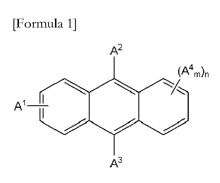
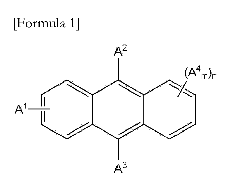
- the anthracene derivative may be represented by Formula 1. wherein, A 1 to A 4 is independently selected from the group consisting of hydrogen, a C 1 -C 6 alkyl group, a C 1 -C 6 alkoxy group, a C 6 -C 18 aryloxy group, a C 6 -C 20 aryl group, a C 3 to C 20 heteroaryl group, an amino group, an alkylamino group, an arylamino group, a cyano group, a nitro group, a hydroxyl group, and a halogen atom, m may be an integer of 1 to 4, n may be an integer of 0 to 4, and at least one of A 1 to A 4 is deuterium or a substituent including deuterium.
- the organic layer according to the present invention in its second aspect may be an organic light emission layer.
- the organic layer or the organic material according to the present invention in any of its aspects may further include a dopant material.
- the dopant material may include a substituted or unsubstituted styrene, a substituted or unsubstituted perylene, a substituted or unsubstituted pyrene, a substituted or unsubstituted arylethylbenzene, a substituted or unsubstituted paraphenylene, a substituted or unsubstituted thiophene, a chelate metal complex, or combinations thereof.
- the dopant material may include a compound of which a constituent is substituted with deuterium.
- the dopant material may include an anthracene derivative of which at least one constituent is substituted with deuterium.
- An organic material having improved heat resistance may be provided.
- An OLED display having improved reliability and a lengthened life span by the organic material may be implemented.
- substituted refers to a hydrogen atom of a compound substituted with a substituent selected from among halogen atoms (F, Br, Cl, or I), a hydroxyl group, an alkoxy group, a nitro group, a cyano group, an amino group, an azido group, an amidino group, a hydrazino group, a hydrazono group, a carbonyl group, a carbamyl group, a thiol group, an ester group, a carboxyl group or its salt, a sulfonic acid group or its salt, a phosphoric acid or its salt, an alkyl group, a C 2 -C 16 alkenyl group, a C 2 -C 16 alkynyl group, an aryl group, a C 7 -C 13 arylakyl group, a C 1 -C 4 oxyalkyl group, a C 1 -C 4 oxyalkyl group, a C 1 -C
- hetero refers to containing one to three hetero atoms selected from among N, O, S, or P.
- the thickness and/or relative thickness of the elements may be exaggerated in order to clarify embodiments of the present invention. Also, the expressions related to positions such as “upper part”, “lower part”, or the like are relatively used for clarification, without limiting absolute positions among the elements.
- the organic material may be used to form an organic light emission layer or an auxiliary layer within the OLED display.
- the auxiliary layer may be one of a hole injection layer, a hole transport layer, an electron injection layer, and an electron transport layer.
- the organic material includes an anthracene derivative of which at least one constituent is substituted with deuterium.
- the anthracene derivative may be represented by Formula 1. wherein, A 1 to A 4 are independently selected from the group consisting of hydrogen, a C 1 -C 6 alkyl group, a C 1 -C 6 alkoxy group, a C 6- C 18 aryloxy group, a C 6 -C 20 aryl group, a C 3 -C 20 heteroaryl group, an amino group, an alkylamino group, an arylamino group, a cyano group, a nitro group, a hydroxyl group, and a halogen atom, m is an integer of 1 to 4, n is an integer of 0 to 4, and at least one of A 1 to A 4 is deuterium or a substituent including deuterium.
- the C 1 -C 6 alkyl group includes a methyl group, an ethyl group, an n-propyl group, an i-propyl group, an n-butyl group, an i-butyl group, a sec-butyl group, a t-butyl group, an i-pentyl group, a t-pentyl group, a neopentyl group, an n-hexyl group, and an i-hexyl group.
- the C 1 -C 6 alkoxy group includes a methoxy group, an ethoxy group, an n-propoxy group, an i-propoxy group, an n-butyloxy group, an i-butyloxy group, a sec-butyloxy group, an i-pentyloxy group, a t-pentyloxy group, and an n-hexyloxy group.
- the C 6- C 18 aryloxy group includes a phenoxy group and a naphthyloxy group.
- the C 6 -C 20 aryl group includes a phenyl group and a naphthyl group.
- the alkylamino group includes NHR and NR 2 .
- the alkyl group (R) of the alkylamino group may be selected from a C 1 -C 6 alkyl group.
- the arylamino group includes -NHAr and NAr 2 .
- the aryl group (Ar) of the arylamino group may be selected from a C 6 -C 20 aryl group.
- the halogen atom includes fluorine, chlorine, bromine, and iodine.
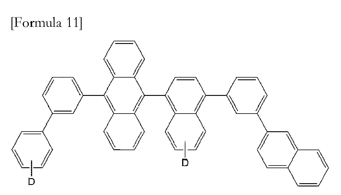
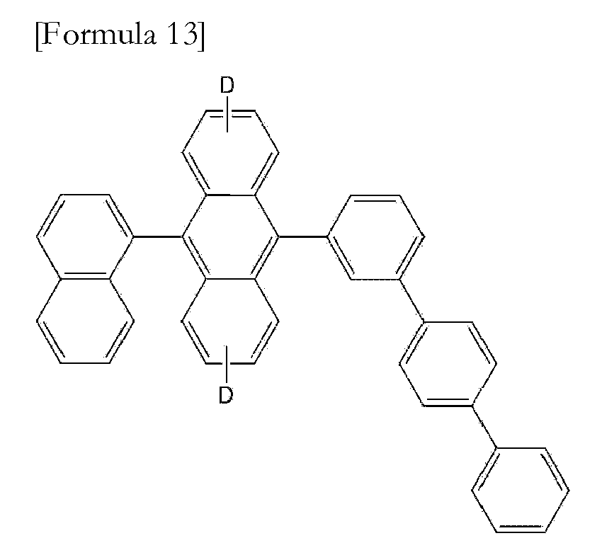
- the anthracene derivative may include a compound represented by one of Formula 2 to Formula 14.
- D is deuterium
- the deuterium may be included on an anthracenyl group and/or on other functional groups.
- at least one hydrogen of the anthracenyl group and/or naphthyl group may be substituted with a deuterium atom.
- a plurality of hydrogen atoms of the organic compound may be substituted with deuterium atoms.
- the organic compound according to one embodiment includes deuterium, it may have a relatively high molecular weight. Accordingly, the glass transition temperature, the melting point, or the like, that are affected by the molecular weight, may be increased. Thus, heat resistance of the organic material including the organic compound may be improved.
- the organic material may include a dopant material.
- the dopant material may include substituted or unsubstituted styrene, a substituted or unsubstituted perylene, a substituted or unsubstituted pyrene, a substituted or unsubstituted arylethylbenzene, a substituted or unsubstituted paraphenylene, a substituted or unsubstituted thiophene, a chelate metal complex, or combinations thereof.
- the dopant material may include at least one selected from among compounds represented by Formula 15 to Formula 23.
- R 1 may be selected from the group consisting of a hydrogen atom, a methyl group, and a t-butyl group.
- Ar 4 may be selected from a C 6 -C 20 aryl group.
- Ar 5 may be selected from a C 6 -C 14 aryl group.
- the dopant material may include a compound represented by Formula 24 shown below.
- a 5 to A 8 are independently selected from the group consisting of hydrogen, a C 1 -C 6 alkyl group, a C 1 -C 6 alkoxy group, a C 6 -C 18 aryloxy group, a C 6 -C 20 aryl group, an amino group, an alkylamino group, an arylamino group, a cyano group, a nitro group, a hydroxyl group, and a halogen atom, 1 is an integer of 0 to 4, o is an integer of 0 to 4, and at least one of A 5 to A 8 is deuterium or a substituent including deuterium.
- the compound represented by Formula 24 may be a compound having different substituents from those of the compound represented by Formula 1 above.
- the C 1 -C 6 alkyl group includes a methyl group, an ethyl group, an n-propyl group, an i-propyl group, an n-butyl group, an i-butyl group, a sec-butyl group, a t-butyl group, an i-pentyl group, a t-pentyl group, a neopentyl group, an n-hexyl group, and an i-hexyl group.
- the C 1 -C 6 alkoxy group includes a methoxy group, an ethoxy group, an n-propoxy group, an i-propoxy group, an n-butyloxy group, an i-butyloxy group, a sec-butyloxy group, an i-pentyloxy group, a t-pentyloxy group, and an n-hexyloxy group.
- the C 6 -C 18 aryloxy group includes a phenoxy group and a naphthyloxy group.
- the C 6 -C 20 aryl group includes a phenyl group and a naphthyl group.
- the alkylamino group includes NHR and NR 2 .
- the alkyl group (R) of the alkylamino group may be selected from a C 1 -C 6 alkyl group.
- the arylamino group includes -NHAr and NAr 2 .
- the aryl group (Ar) of the arylamino group may be selected from a C 6 -C 20 aryl group.
- the halogen atom includes fluorine, chlorine, bromine, and iodine.
- the heat resistance of the organic material may be further improved.
- Figure 1 is a cross-sectional view of an OLED display according to an exemplary embodiment.
- a lower electrode 120 and an upper electrode 160 are disposed on a substrate 110, and an organic light emission layer 140 is disposed between the lower electrode 120 and the upper electrode 160.
- a lower auxiliary layer 130 may be interposed between the lower electrode 120 and the organic light emission layer 140.
- An upper auxiliary layer 150 may be interposed between the organic light emission layer 140 and the upper electrode 160.
- the substrate 110 may made of glass, polymer, or a combination thereof.
- One of the lower electrode 120 and the upper electrode 160 may be an anode and the other may be a cathode.
- the lower electrode 120 and the upper electrode 160 may be transparent or opaque electrodes.
- the lower electrode 120 and the upper electrode 160 may be made of ITO, IZO, or a combination thereof, or may be made of aluminum (Al), silver (Ag), or a combination thereof.
- One of the lower auxiliary layer 130 and the upper auxiliary layer 150 may include a hole injection layer and/or a hole transport layer, and the other may include an electron transport layer and/or an electron injection layer.
- the lower auxiliary layer 130 may include a hole injection layer and/or a hole transport layer and the upper auxiliary layer 150 may include an electron injection layer and/or an electron transport layer.
- at least one of the lower auxiliary layer 130 and the upper auxiliary layer 150 may be omitted.
- the organic material according to an exemplary embodiment may be included in the lower auxiliary layer 130, the organic light emission layer 140, the upper auxiliary layer 150, or any combination thereof.
- the organic material may be included in the organic light emission layer 140.
- the organic material may include a host material and a dopant material mixed in the host material.
- the blue host material includes an anthracene derivative including at least one deuterium.
- an anthracene derivative including at least one deuterium.
- at least one of hydrogen atoms of an anthracenyl group may be substituted by a deuterium atom or at least one of hydrogen atoms of a functional group other than the anthracenyl group may be substituted by a deuterium atom.
- a hydrogen atom of the anthracenyl group and a hydrogen atom of a substituent other than the anthracenyl group may be simultaneously substituted with deuterium atoms.
- the blue host material may include a compound represented by Formula 1.
- a 1 to A 4 are independently selected from the group consisting of hydrogen, a C 1 -C 6 alkyl group, a C 1 -C 6 alkoxy group, a C 6 -C 18 aryloxy group, a C 6 -C 20 aryl group, a C 3 -C 20 heteroaryl group, an amino group, an alkylamino group, an arylamino group, a cyano group, a nitro group, a hydroxyl group, and a halogen atom, m is an integer of 1 to 4, n is an integer of 0 to 4, and at least one of A 1 to A 4 is deuterium or a substituent including deuterium.
- the C 1 -C 6 alkyl group includes a methyl group, an ethyl group, an n-propyl group, an i-propyl group, an n-butyl group, an i-butyl group, a sec-butyl group, a t-butyl group, an i-pentyl group, a t-pentyl group, a neopentyl group, an n-hexyl group, and an i-hexyl group.
- the C 1 -C 6 alkoxy group includes a methoxy group, an ethoxy group, an n-propoxy group, an i-propoxy group, an n-butyloxy group, an i-butyloxy group, a sec-butyloxy group, an i-pentyloxy group, a t-pentyloxy group, and an n-hexyloxy group.
- the C 6 -C 18 aryloxy group includes a phenoxy group and a naphthyloxy group.
- the C 6 -C 20 aryl group includes a phenyl group and a naphthyl group.
- the C 6 -C 20 aryl group includes a phenyl group and a naphthyl group.
- the alkyl group (R) of the alkylamino group may be selected from a C 1 -C 6 alkyl group.
- the arylamino group includes -NHAr and NAr 2 .
- the aryl group (Ar) of the arylamino group may be selected from a C 6 -C 20 aryl group.
- the halogen atom includes fluorine, chlorine, bromine, and iodine.
- the blue host material may include at least one selected from among compounds represented by Formula 2 to Formula 14.
- D is deuterium
- the molecular weight of the compound is increased by the deuterium.
- the increase in the molecular weight of the compound may lead to an increase in a melting point and/or glass transition temperature of the organic material including the blue host material. Accordingly, heat resistance of the organic light emission layer 140 including the blue host material may be improved.
- the reliability of the OLED display including the blue host material may be improved and a life span of the OLED display may be lengthened.
- the organic light emission layer 140 may selectively further include hosts of different colors.
- the organic light emission layer 140 may further include red hosts and/or green hosts therein.
- the organic emission layer 140 may include a dopant material.
- the dopant material may be, for example, a substituted or unsubstituted styrene, a substituted or unsubstituted perylene, a substituted or unsubstituted pyrene, a substituted or unsubstituted arylethylbenzene, a substituted or unsubstituted paraphenylene, a substituted or unsubstituted thiophene, a chelate metal complex, or combinations thereof.
- the dopant material may include at least one selected from among compounds represented by Formula 15 to Formula 23.
- each R 1 is independently selected from the group consisting of hydrogen, a methyl group, and a t-butyl group.
- Ar 4 is selected from a C 6 -C 20 aryl group.
- Ar 4 is selected from a C 6 -C 14 aryl group.
- the dopant material may include a compound of which a constituent has been substituted with deuterium.
- the dopant material may be selected from compounds represented by Formula 15 to Formula 23, and the selected compound may be substituted with deuterium.
- the dopant material may include a compound represented by Formula 24 shown below.
- a 5 to A 8 are independently selected from the group consisting of hydrogen, a C 1 -C 6 alkyl group, a C 1 -C 6 alkoxy group, a C 6 -C 18 aryloxy group, a C 6 -C 20 aryl group, an amino group, an alkylamino group, an arylamino group, a cyano group, a nitro group, a hydroxyl group, and a halogen atom, 1 is an integer of 0 to 4, o is an integer of 0 to 4, and at least one of A 5 to A 8 is deuterium or a substituent including deuterium.
- the compound represented by Formula 24 may be a compound that is different from that used as the host material.
- the C 1 -C 6 alkyl group includes a methyl group, an ethyl group, an n-propyl group, an i-propyl group, an n-butyl group, an i-butyl group, a sec-butyl group, a t-butyl group, an i-pentyl group, a t-pentyl group, a neopentyl group, an n-hexyl group, and an i-hexyl group.
- the C 1 -C 6 alkoxy group includes a methoxy group, an ethoxy group, an n-propoxy group, an i-propoxy group, an n-butyloxy group, an i-butyloxy group, a sec-butyloxy group, an i-pentyloxy group, a t-pentyloxy group, and an n-hexyloxy group.
- the C 6 -C 18 aryloxy group includes a phenoxy group and a naphthyloxy group.
- the C 6 -C 20 aryl group includes a phenyl group and a naphthyl group.
- the alkylamino group includes NHR and NR 2 .
- the alkyl group (R) of the alkylamino group may be selected from a C 1 -C 6 alkyl group.
- the arylamino group includes -NHAr and NAr 2 .
- the aryl group (Ar) of the arylamino group may be selected from a C 6 -C 20 alkyl group.
- the halogen atom includes fluorine, chlorine, bromine, and iodine.
- the heat resistance of the organic material may be further improved.
- Figure 2 is a cross-sectional view of an OLED display according to another exemplary embodiment.
- organic light emission layers 140 and 142 may include a plurality of stacked layers.
- the layers emit light of different colors, respectively, and the combination of the stacked layers may emit white light.
- the lower light emission layer 140 may emit blue light
- the upper light emission layer 142 may emit light of a different color other than blue color
- the stacked lower and upper light emission layers 140 and 142 may emit white light.
- the upper electrode 160 may be disposed on the upper light emission layer 140, and color filters 172, 174, and 176 may be disposed on the upper electrode 160. As the white light emitted through the organic light emission layers 140 and 142 passes through the color filters 172, 174, and 176, it may be converted into red, blue, and green colors. Alternatively, color filters of any other colors may be disposed on the upper electrode 160, and light beams of different colors may be emitted.
- ITO electrode was formed on a glass substrate, on which 4,4',4"-tris (3-methylphenylamino)triphenylamine (MTDATA), 1,4,5,8,9,12-hexaazatriphenylenehexanitrile (HAT-CN6), and N,N'-diphenyl-N,N'-di(1-naphthyl)-1,1'-biphenyl-4,4'-diamine (NPB) were then deposited to have thicknesses of about 70nm, 5nm, and 70nm, respectively.
- MTDATA 3,-methylphenylamino)triphenylamine
- HAT-CN6 1,4,5,8,9,12-hexaazatriphenylenehexanitrile
- NPB N,N'-diphenyl-N,N'-di(1-naphthyl)-1,1'-biphenyl-4,4'-diamine
- a mixture obtained by mixing a compound represented by Formula 23 and a compound represented by Formula 16 was deposited on the resultant structure to form an organic light emission layer.
- the compound represented by Formula 16 was mixed with the concentration of 3 wt% based on the compound represented by Formula 23, and used as a dopant of the organic light emission layer.
- BCP 2,9-dimethyl-4,7-diphenyl-1,10-phenanthroline
- LiQ 8-hydroxyquinolinate lithium
- magnesium and silver were deposited in the weight ratio of 160 : 10 to form an upper electrode on the organic light emission layer. As a result, an OLED display was fabricated.
- An OLED display was fabricated in the same manner as that of the Example 1, except that the compound represented by formula 16 as a dopant was used at the concentration of about 2 wt% based on the compound represented by Formula 23.
- An OLED display was fabricated in the same manner as that of the Example 1, except that the compound represented by formula 16 as a dopant was used at the concentration of about 1 wt% based on the compound represented by Formula 23.
- An OLED display was fabricated in the same manner as those of Example 1, except that the compound represented by Formula 23 was replaced with 2,9,10-tris(2-naphthyl)anthracene.
- the luminance of each of the OLED displays fabricated according to the Examples 1 to 3 and Comparative Example 1 according to time was measured.
- the change in the luminance over time was measured by applying a constant current of about 39 mA/cm 2 to the respective OLED displays, at room temperature, according to the highly accelerated life test.
- a luminance reduction rate of each of the OLED displays according to Examples 1 to 3 is smaller than that of the OLED display according to Comparative Example 1. It is noted that the OLED displays according to Examples 1 to 3 have stable luminance characteristics. Therefore, the OLED displays may be implemented with improved reliability.
Landscapes
- Chemical & Material Sciences (AREA)
- Physics & Mathematics (AREA)
- Engineering & Computer Science (AREA)
- Materials Engineering (AREA)
- Spectroscopy & Molecular Physics (AREA)
- Organic Chemistry (AREA)
- Inorganic Chemistry (AREA)
- Optics & Photonics (AREA)
- Electroluminescent Light Sources (AREA)
Abstract
Description
- The present invention relates to an organic material for an organic light emitting diode (OLED) display, and an OLED display using the same.
- An OLED display includes two electrodes facing each other and an organic layer interposed between the two electrodes. In the OLED display, holes injected from one electrode and electrons injected from the other electrode are combined in the organic layer to form excitons, and as the excitons generate energy, light is emitted. The OLED display may be applicable to various fields including a display device and an illumination system.
- The OLED display may be driven by using self-emission characteristics of an organic light emission layer, so it does not necessarily require an auxiliary light source. Thus, less power is consumed for driving the OLED display. In addition, because the OLED display has a wide viewing angle and a fast response speed, it is receiving much attention as a next-generation display device.
- The OLED display includes several organic layers including an organic light emission layer. However, an organic material of the organic layer is generally weak to heat, so it is easily degraded according to a change in temperature.
- The present invention provides an organic material having improved heat resistance. The present invention also provides an organic light emitting diode (OLED) display including the organic material.
- In a first aspect of the present invention, there is provided an organic material for an organic light emitting diode (OLED) display including an anthracene derivative of which at least one constituent is substituted with deuterium.
- In a second aspect of the present invention, there is provided an OLED display including first and second electrodes, and an organic layer interposed between the first and second electrodes, wherein the organic layer includes an organic material according to the present invention in its first aspect
- In a third aspect of the present invention, there is provided the use of an organic material according to the present invention in its first aspect in an organic light emitting diode (OLED) display.
- In embodiments of the present invention, the anthracene derivative may be represented by Formula 1.
- The organic layer according to the present invention in its second aspect may be an organic light emission layer. The organic layer or the organic material according to the present invention in any of its aspects may further include a dopant material.
- The dopant material may include a substituted or unsubstituted styrene, a substituted or unsubstituted perylene, a substituted or unsubstituted pyrene, a substituted or unsubstituted arylethylbenzene, a substituted or unsubstituted paraphenylene, a substituted or unsubstituted thiophene, a chelate metal complex, or combinations thereof.
- The dopant material may include a compound of which a constituent is substituted with deuterium.
- The dopant material may include an anthracene derivative of which at least one constituent is substituted with deuterium.
- An organic material having improved heat resistance may be provided. An OLED display having improved reliability and a lengthened life span by the organic material may be implemented.
- Further embodiments of the present invention in any of its various aspects are as described below or as defined in the sub-claims.
- A more complete appreciation of the present invention, and many of the attendant advantages thereof, will be readily apparent as the same becomes better understood by reference to the following detailed description when considered in conjunction with the accompanying drawings, wherein:
-
Figure 1 is a view for explaining an organic light emitting diode (OLED) display according to an embodiment of the present invention. -
Figure 2 is a view for explaining an organic light emitting diode (OLED) display according to another embodiment of the present invention. -
Figure 3 is a graph showing change in luminance of the OLED displays according to the embodiments of the present invention described in Examples 1 to 3 and the Comparative Example over time. - An organic material and an organic light emitting diode (OLED) display using the same according to exemplary embodiments of the present invention will now be described. The exemplary embodiments described herein are provided to allow a skilled person in the art to easily understand the idea of the present invention, and the present invention is not meant to be limited thereto. The exemplary embodiments described herein may be modified within the technical idea and scope of the present invention.
- In the present exemplary embodiments, unless otherwise specified, "substituted" refers to a hydrogen atom of a compound substituted with a substituent selected from among halogen atoms (F, Br, Cl, or I), a hydroxyl group, an alkoxy group, a nitro group, a cyano group, an amino group, an azido group, an amidino group, a hydrazino group, a hydrazono group, a carbonyl group, a carbamyl group, a thiol group, an ester group, a carboxyl group or its salt, a sulfonic acid group or its salt, a phosphoric acid or its salt, an alkyl group, a C2-C16 alkenyl group, a C2-C16 alkynyl group, an aryl group, a C7-C13 arylakyl group, a C1-C4 oxyalkyl group, a C1-C20 heteroalkyl group, a C3-C20 heteroaryl alkyl group, a cycloalkyl group, a C3-C15 cycloalkenyl group, a C6-C15 cycloalkynyl group, a heterocycloalkyl group, and combinations thereof.
- Also, unless otherwise specified, "hetero" refers to containing one to three hetero atoms selected from among N, O, S, or P.
- In the present exemplary embodiments, "and/or" is used to include at least one among constituent elements arranged before and after. In the present exemplary embodiments, each element and/or parts are designated by using expressions such as "first", "second", etc., but these are used for clarification and the present invention is not limited thereto.
- In the present exemplary embodiments, it will be understood that when an element is referred to as being "on" another element, it can be directly on the other element or intervening elements may also be present.
- In the drawings, the thickness and/or relative thickness of the elements may be exaggerated in order to clarify embodiments of the present invention. Also, the expressions related to positions such as "upper part", "lower part", or the like are relatively used for clarification, without limiting absolute positions among the elements.
- An organic material for an OLED display according to the present invention in its first aspect will now be described.
- The organic material may be used to form an organic light emission layer or an auxiliary layer within the OLED display. Here, the auxiliary layer may be one of a hole injection layer, a hole transport layer, an electron injection layer, and an electron transport layer.
- The organic material includes an anthracene derivative of which at least one constituent is substituted with deuterium.
- The anthracene derivative may be represented by Formula 1.
- The C1-C6 alkyl group includes a methyl group, an ethyl group, an n-propyl group, an i-propyl group, an n-butyl group, an i-butyl group, a sec-butyl group, a t-butyl group, an i-pentyl group, a t-pentyl group, a neopentyl group, an n-hexyl group, and an i-hexyl group.
- The C1-C6 alkoxy group includes a methoxy group, an ethoxy group, an n-propoxy group, an i-propoxy group, an n-butyloxy group, an i-butyloxy group, a sec-butyloxy group, an i-pentyloxy group, a t-pentyloxy group, and an n-hexyloxy group.
- The C6-C18 aryloxy group includes a phenoxy group and a naphthyloxy group.
- The C6-C20 aryl group includes a phenyl group and a naphthyl group.
- The alkylamino group includes NHR and NR2. The alkyl group (R) of the alkylamino group may be selected from a C1-C6 alkyl group.
- The arylamino group includes -NHAr and NAr2. The aryl group (Ar) of the arylamino group may be selected from a C6-C20 aryl group.
- The halogen atom includes fluorine, chlorine, bromine, and iodine.
- For example, the anthracene derivative may include a compound represented by one of Formula 2 to Formula 14.


- In
Formula 2 to Formula 14, D is deuterium. - In Formula 2 to Formula 14, the deuterium may be included on an anthracenyl group and/or on other functional groups. For example, in
Formula 2, at least one hydrogen of the anthracenyl group and/or naphthyl group may be substituted with a deuterium atom. In an exemplary embodiment, a plurality of hydrogen atoms of the organic compound may be substituted with deuterium atoms. - Because the organic compound according to one embodiment includes deuterium, it may have a relatively high molecular weight. Accordingly, the glass transition temperature, the melting point, or the like, that are affected by the molecular weight, may be increased. Thus, heat resistance of the organic material including the organic compound may be improved.
- The organic material may include a dopant material. For example, when the organic material is used as a material of an organic light emission layer, the dopant material may include substituted or unsubstituted styrene, a substituted or unsubstituted perylene, a substituted or unsubstituted pyrene, a substituted or unsubstituted arylethylbenzene, a substituted or unsubstituted paraphenylene, a substituted or unsubstituted thiophene, a chelate metal complex, or combinations thereof.
- For example, the dopant material may include at least one selected from among compounds represented by Formula 15 to Formula 23.


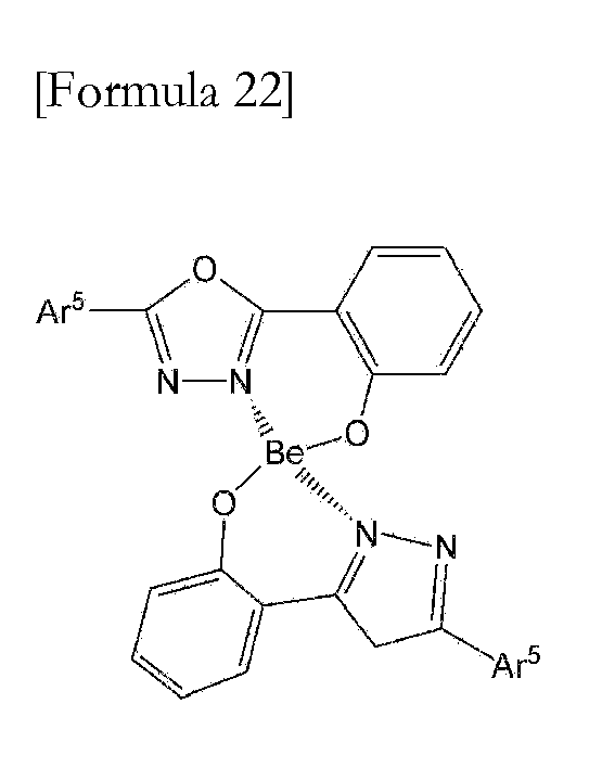

- In Formula 15, R1 may be selected from the group consisting of a hydrogen atom, a methyl group, and a t-butyl group. In Formula 19, Ar4 may be selected from a C6-C20 aryl group. In Formula 22, Ar5 may be selected from a C6-C14 aryl group.
- In an exemplary embodiment, at least one of hydrogen atoms of the compound constituting the dopant material may be substituted with deuterium. For example, the dopant material may include a compound represented by Formula 24 shown below.

- In Formula 24, A5 to A8 are independently selected from the group consisting of hydrogen, a C1-C6 alkyl group, a C1-C6 alkoxy group, a C6-C18 aryloxy group, a C6-C20 aryl group, an amino group, an alkylamino group, an arylamino group, a cyano group, a nitro group, a hydroxyl group, and a halogen atom, 1 is an integer of 0 to 4, o is an integer of 0 to 4, and at least one of A5 to A8 is deuterium or a substituent including deuterium. The compound represented by Formula 24 may be a compound having different substituents from those of the compound represented by
Formula 1 above. - The C1-C6 alkyl group includes a methyl group, an ethyl group, an n-propyl group, an i-propyl group, an n-butyl group, an i-butyl group, a sec-butyl group, a t-butyl group, an i-pentyl group, a t-pentyl group, a neopentyl group, an n-hexyl group, and an i-hexyl group.
- The C1-C6 alkoxy group includes a methoxy group, an ethoxy group, an n-propoxy group, an i-propoxy group, an n-butyloxy group, an i-butyloxy group, a sec-butyloxy group, an i-pentyloxy group, a t-pentyloxy group, and an n-hexyloxy group.
- The C6-C18 aryloxy group includes a phenoxy group and a naphthyloxy group.
- The C6-C20 aryl group includes a phenyl group and a naphthyl group.
- The alkylamino group includes NHR and NR2. The alkyl group (R) of the alkylamino group may be selected from a C1-C6 alkyl group.
- The arylamino group includes -NHAr and NAr2. The aryl group (Ar) of the arylamino group may be selected from a C6-C20 aryl group.
- The halogen atom includes fluorine, chlorine, bromine, and iodine.
- When the dopant material includes a compound including deuterium, the heat resistance of the organic material may be further improved.
- An OLED display including the foregoing organic material, according to the present invention in its second aspect, will now be described with reference to
Figure 1 . -
Figure 1 is a cross-sectional view of an OLED display according to an exemplary embodiment. - With reference to
Figure 1 , alower electrode 120 and anupper electrode 160 are disposed on asubstrate 110, and an organiclight emission layer 140 is disposed between thelower electrode 120 and theupper electrode 160. A lowerauxiliary layer 130 may be interposed between thelower electrode 120 and the organiclight emission layer 140. An upperauxiliary layer 150 may be interposed between the organiclight emission layer 140 and theupper electrode 160. - The
substrate 110 may made of glass, polymer, or a combination thereof. - One of the
lower electrode 120 and theupper electrode 160 may be an anode and the other may be a cathode. Thelower electrode 120 and theupper electrode 160 may be transparent or opaque electrodes. For example, thelower electrode 120 and theupper electrode 160 may be made of ITO, IZO, or a combination thereof, or may be made of aluminum (Al), silver (Ag), or a combination thereof. - One of the lower
auxiliary layer 130 and the upperauxiliary layer 150 may include a hole injection layer and/or a hole transport layer, and the other may include an electron transport layer and/or an electron injection layer. For example, when thelower electrode 120 is an anode and theupper electrode 150 is a cathode, the lowerauxiliary layer 130 may include a hole injection layer and/or a hole transport layer and the upperauxiliary layer 150 may include an electron injection layer and/or an electron transport layer. In this case, at least one of the lowerauxiliary layer 130 and the upperauxiliary layer 150 may be omitted. - The organic material according to an exemplary embodiment may be included in the lower
auxiliary layer 130, the organiclight emission layer 140, the upperauxiliary layer 150, or any combination thereof. For example, the organic material may be included in the organiclight emission layer 140. Here, the organic material may include a host material and a dopant material mixed in the host material. - Hereinafter, the case in which the organic material is included in a blue host material will be described, but the present invention is not meant to be limited thereto.
- The blue host material includes an anthracene derivative including at least one deuterium. In the anthracene derivative, at least one of hydrogen atoms of an anthracenyl group may be substituted by a deuterium atom or at least one of hydrogen atoms of a functional group other than the anthracenyl group may be substituted by a deuterium atom. Alternatively, in the anthracene derivative, a hydrogen atom of the anthracenyl group and a hydrogen atom of a substituent other than the anthracenyl group may be simultaneously substituted with deuterium atoms.
- For example, the blue host material may include a compound represented by
Formula 1.
- In
Formula 1, A1 to A4 are independently selected from the group consisting of hydrogen, a C1-C6 alkyl group, a C1-C6 alkoxy group, a C6-C18 aryloxy group, a C6-C20 aryl group, a C3-C20 heteroaryl group, an amino group, an alkylamino group, an arylamino group, a cyano group, a nitro group, a hydroxyl group, and a halogen atom, m is an integer of 1 to 4, n is an integer of 0 to 4, and at least one of A1 to A4 is deuterium or a substituent including deuterium. - The C1-C6 alkyl group includes a methyl group, an ethyl group, an n-propyl group, an i-propyl group, an n-butyl group, an i-butyl group, a sec-butyl group, a t-butyl group, an i-pentyl group, a t-pentyl group, a neopentyl group, an n-hexyl group, and an i-hexyl group.
- The C1-C6 alkoxy group includes a methoxy group, an ethoxy group, an n-propoxy group, an i-propoxy group, an n-butyloxy group, an i-butyloxy group, a sec-butyloxy group, an i-pentyloxy group, a t-pentyloxy group, and an n-hexyloxy group.
- The C6-C18 aryloxy group includes a phenoxy group and a naphthyloxy group.
- The C6-C20 aryl group includes a phenyl group and a naphthyl group.
- The C6-C20 aryl group includes a phenyl group and a naphthyl group. The alkyl group (R) of the alkylamino group may be selected from a C1-C6 alkyl group.
- The arylamino group includes -NHAr and NAr2. The aryl group (Ar) of the arylamino group may be selected from a C6-C20 aryl group.
- The halogen atom includes fluorine, chlorine, bromine, and iodine.
- For example, the blue host material may include at least one selected from among compounds represented by
Formula 2 toFormula 14.


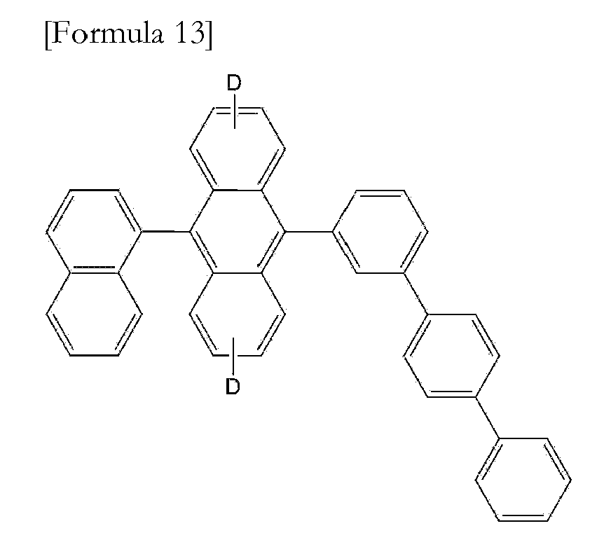

- In
Formula 2 toFormula 14, D is deuterium. - The molecular weight of the compound is increased by the deuterium. The increase in the molecular weight of the compound may lead to an increase in a melting point and/or glass transition temperature of the organic material including the blue host material. Accordingly, heat resistance of the organic
light emission layer 140 including the blue host material may be improved. Thus, the reliability of the OLED display including the blue host material may be improved and a life span of the OLED display may be lengthened. - The organic
light emission layer 140 may selectively further include hosts of different colors. For example, the organiclight emission layer 140 may further include red hosts and/or green hosts therein. - The
organic emission layer 140 may include a dopant material. The dopant material may be, for example, a substituted or unsubstituted styrene, a substituted or unsubstituted perylene, a substituted or unsubstituted pyrene, a substituted or unsubstituted arylethylbenzene, a substituted or unsubstituted paraphenylene, a substituted or unsubstituted thiophene, a chelate metal complex, or combinations thereof. - For example, the dopant material may include at least one selected from among compounds represented by Formula 15 to Formula 23.


- In Formula 15, each R1 is independently selected from the group consisting of hydrogen, a methyl group, and a t-butyl group. In Formula 19, Ar4 is selected from a C6-C20 aryl group. For example, in Formula 19, Ar4 is selected from a C6-C14 aryl group.
- In an exemplary embodiment, the dopant material may include a compound of which a constituent has been substituted with deuterium. For example, the dopant material may be selected from compounds represented by Formula 15 to Formula 23, and the selected compound may be substituted with deuterium. For another example, the dopant material may include a compound represented by Formula 24 shown below.

- In Formula 24, A5 to A8 are independently selected from the group consisting of hydrogen, a C1-C6 alkyl group, a C1-C6 alkoxy group, a C6-C18 aryloxy group, a C6-C20 aryl group, an amino group, an alkylamino group, an arylamino group, a cyano group, a nitro group, a hydroxyl group, and a halogen atom, 1 is an integer of 0 to 4, o is an integer of 0 to 4, and at least one of A5 to A8 is deuterium or a substituent including deuterium. The compound represented by Formula 24 may be a compound that is different from that used as the host material.
- The C1-C6 alkyl group includes a methyl group, an ethyl group, an n-propyl group, an i-propyl group, an n-butyl group, an i-butyl group, a sec-butyl group, a t-butyl group, an i-pentyl group, a t-pentyl group, a neopentyl group, an n-hexyl group, and an i-hexyl group.
- The C1-C6 alkoxy group includes a methoxy group, an ethoxy group, an n-propoxy group, an i-propoxy group, an n-butyloxy group, an i-butyloxy group, a sec-butyloxy group, an i-pentyloxy group, a t-pentyloxy group, and an n-hexyloxy group.
- The C6-C18 aryloxy group includes a phenoxy group and a naphthyloxy group.
- The C6-C20 aryl group includes a phenyl group and a naphthyl group.
- The alkylamino group includes NHR and NR2. The alkyl group (R) of the alkylamino group may be selected from a C1-C6 alkyl group.
- The arylamino group includes -NHAr and NAr2. The aryl group (Ar) of the arylamino group may be selected from a C6-C20 alkyl group.
- The halogen atom includes fluorine, chlorine, bromine, and iodine.
- When the dopant material includes a compound including deuterium, the heat resistance of the organic material may be further improved.
- An OLED display including the organic material according to an exemplary embodiment will now be described with reference to
Figure 2 . The same reference numerals are used for the same elements as those described above with reference toFigure 1 , and descriptions thereof will be omitted. -
Figure 2 is a cross-sectional view of an OLED display according to another exemplary embodiment. - With reference to
Figure 2 , organic light emission layers 140 and 142 may include a plurality of stacked layers. The layers emit light of different colors, respectively, and the combination of the stacked layers may emit white light. For example, the lowerlight emission layer 140 may emit blue light, the upperlight emission layer 142 may emit light of a different color other than blue color, and the stacked lower and upper light emission layers 140 and 142 may emit white light. - The
upper electrode 160 may be disposed on the upperlight emission layer 140, andcolor filters upper electrode 160. As the white light emitted through the organic light emission layers 140 and 142 passes through thecolor filters upper electrode 160, and light beams of different colors may be emitted. - The present invention will be described in detail through the following exemplary embodiments. The following exemplary embodiments are merely described for the purpose of explanation, without limiting the scope of the present invention.
- An ITO electrode was formed on a glass substrate, on which 4,4',4"-tris (3-methylphenylamino)triphenylamine (MTDATA), 1,4,5,8,9,12-hexaazatriphenylenehexanitrile (HAT-CN6), and N,N'-diphenyl-N,N'-di(1-naphthyl)-1,1'-biphenyl-4,4'-diamine (NPB) were then deposited to have thicknesses of about 70nm, 5nm, and 70nm, respectively.
- A mixture obtained by mixing a compound represented by Formula 23 and a compound represented by Formula 16 was deposited on the resultant structure to form an organic light emission layer. The compound represented by Formula 16 was mixed with the concentration of 3 wt% based on the compound represented by Formula 23, and used as a dopant of the organic light emission layer.
- Then, a mixture of 2,9-dimethyl-4,7-diphenyl-1,10-phenanthroline (BCP) and 8-hydroxyquinolinate lithium (LiQ) was deposited on the organic light emission layer. In this case, the BCP and the LiQ were mixed in the ratio of 50 wt% : 50 wt%.
- Thereafter, magnesium and silver were deposited in the weight ratio of 160 : 10 to form an upper electrode on the organic light emission layer. As a result, an OLED display was fabricated.


- An OLED display was fabricated in the same manner as that of the Example 1, except that the compound represented by formula 16 as a dopant was used at the concentration of about 2 wt% based on the compound represented by Formula 23.
- An OLED display was fabricated in the same manner as that of the Example 1, except that the compound represented by formula 16 as a dopant was used at the concentration of about 1 wt% based on the compound represented by Formula 23.
- An OLED display was fabricated in the same manner as those of Example 1, except that the compound represented by Formula 23 was replaced with 2,9,10-tris(2-naphthyl)anthracene.
- The luminance of each of the OLED displays fabricated according to the Examples 1 to 3 and Comparative Example 1 according to time was measured. The change in the luminance over time was measured by applying a constant current of about 39 mA/cm2 to the respective OLED displays, at room temperature, according to the highly accelerated life test.
- A change in the luminance of each of the OLED displays over time was measured at room temperature, and the results are shown in
Figure 3 . - With reference to
Figure 3 , it is noted that a luminance reduction rate of each of the OLED displays according to Examples 1 to 3 is smaller than that of the OLED display according to Comparative Example 1. It is noted that the OLED displays according to Examples 1 to 3 have stable luminance characteristics. Therefore, the OLED displays may be implemented with improved reliability. - While the present invention has been described in relation to certain exemplary embodiments thereof, it is to be understood that the present invention is not limited to such embodiments, but, on the contrary, is intended to cover various modifications and equivalent arrangements included within the scope of the appended claims.
Claims (12)
- An organic material for an organic light emitting diode (OLED) display, comprising an anthracene derivative of which at least one constituent is substituted with deuterium.
- The organic material of claim 1, wherein the anthracene derivative is represented by Formula 1:

m is an integer from 1 to 4, and
n is an integer from 0 to 4. - The organic material of claims 1 or 2, wherein the anthracene derivative is selected from compounds represented by Formula 2 to Formula 14:




- The organic material of claims 1, 2 or 3, further comprising a dopant material.
- The organic material of claim 4, wherein the dopant material comprises a substituted or unsubstituted styrene, a substituted or unsubstituted perylene, a substituted or unsubstituted pyrene, a substituted or unsubstituted arylethylbenzene, a substituted or unsubstituted paraphenylene, a substituted or unsubstituted thiophene, a chelate metal complex, or combinations thereof.
- The organic material of claims 4 or 5, wherein the dopant material is substituted with one or more deuterium atoms.
- The organic material of claim 4, wherein the dopant material comprises an anthracene derivative further substituted with one or more deuterium atoms.
- The organic material of claim 4, wherein the dopant material comprises at least one selected from compounds represented by Formula 15 to Formula 23


- The organic material of claim 8, wherein the dopant material comprises at least one selected from compounds represented by Formula 16 and Formula 23.


- An organic light emitting diode display comprising:first and second electrodes that face each other; andan organic layer interposed between the first and second electrodes,wherein the organic layer comprises an organic material as claimed in any one of claims 1 to 9.
- The organic light emitting diode display of claim 10, wherein the organic layer is an organic emission layer.
- Use of an organic material as claimed in any one of claims 1 to 9 in an organic light emitting diode (OLED) display.
Applications Claiming Priority (1)
| Application Number | Priority Date | Filing Date | Title |
|---|---|---|---|
| KR1020100046507A KR101191644B1 (en) | 2010-05-18 | 2010-05-18 | Organic Materials and Organic Light Emitting Devices Using the Same |
Publications (3)
| Publication Number | Publication Date |
|---|---|
| EP2388843A2 true EP2388843A2 (en) | 2011-11-23 |
| EP2388843A3 EP2388843A3 (en) | 2012-09-19 |
| EP2388843B1 EP2388843B1 (en) | 2019-08-07 |
Family
ID=44168332
Family Applications (1)
| Application Number | Title | Priority Date | Filing Date |
|---|---|---|---|
| EP11166396.9A Active EP2388843B1 (en) | 2010-05-18 | 2011-05-17 | Organic material and organic light emitting diode display using same |
Country Status (4)
| Country | Link |
|---|---|
| US (1) | US9634254B2 (en) |
| EP (1) | EP2388843B1 (en) |
| JP (1) | JP2011241383A (en) |
| KR (1) | KR101191644B1 (en) |
Cited By (2)
| Publication number | Priority date | Publication date | Assignee | Title |
|---|---|---|---|---|
| WO2014106522A1 (en) * | 2013-01-03 | 2014-07-10 | Merck Patent Gmbh | Materials for electronic devices |
| WO2018095384A1 (en) * | 2016-11-23 | 2018-05-31 | 广州华睿光电材料有限公司 | Deuterated fused ring compound, polymer, mixture and composition, and organic electronic device |
Families Citing this family (23)
| Publication number | Priority date | Publication date | Assignee | Title |
|---|---|---|---|---|
| TW201245408A (en) * | 2011-04-08 | 2012-11-16 | Du Pont | Electronic device |
| JP2013227251A (en) * | 2012-04-25 | 2013-11-07 | Jnc Corp | Electron transport material and organic electroluminescent element using the same |
| KR102293729B1 (en) * | 2014-08-14 | 2021-08-27 | 삼성디스플레이 주식회사 | Condensed-cyclic compound and organic light emitting diode comprising the same |
| JP7325731B2 (en) | 2018-08-23 | 2023-08-15 | 国立大学法人九州大学 | organic electroluminescence element |
| WO2020080417A1 (en) | 2018-10-16 | 2020-04-23 | 出光興産株式会社 | Organic electroluminescent element and electronic device |
| CN122555332A (en) * | 2018-10-16 | 2026-08-11 | 出光兴产株式会社 | Organic electroluminescent elements and electronic devices |
| KR20200047400A (en) | 2018-10-26 | 2020-05-07 | 롬엔드하스전자재료코리아유한회사 | A plurality of light-emitting materials and organic electroluminescent device comprising the same |
| WO2020085829A1 (en) * | 2018-10-26 | 2020-04-30 | Rohm And Haas Electronic Materials Korea Ltd. | A plurality of light-emitting materials and organic electroluminescent device comprising the same |
| KR102661411B1 (en) | 2018-12-28 | 2024-04-25 | 엘지디스플레이 주식회사 | Organic light emitting diode and orgnic light emitting device including the same |
| KR102667691B1 (en) * | 2018-12-28 | 2024-05-20 | 엘지디스플레이 주식회사 | Organic light emitting diode and orgnic light emitting device including the same |
| KR102668776B1 (en) | 2018-12-28 | 2024-05-22 | 엘지디스플레이 주식회사 | Organic light emitting diode and orgnic light emitting device including the same |
| JP2020188121A (en) * | 2019-05-14 | 2020-11-19 | 出光興産株式会社 | Organic electroluminescence devices and electronic devices |
| US12522764B2 (en) | 2019-07-31 | 2026-01-13 | Lg Chem, Ltd. | Compound and organic light emitting device comprising same |
| WO2021049651A1 (en) | 2019-09-13 | 2021-03-18 | 出光興産株式会社 | Organic electroluminescent element and electronic device |
| US12666861B2 (en) | 2019-09-13 | 2026-06-23 | Idemitsu Kosan Co., Ltd. | Organic electroluminescent element and electronic device |
| JP7531499B2 (en) * | 2019-09-13 | 2024-08-09 | 出光興産株式会社 | Organic electroluminescence element and electronic device |
| KR102437213B1 (en) * | 2019-11-29 | 2022-08-29 | 주식회사 엘지화학 | Organic light emitting device |
| US12610735B2 (en) | 2019-12-26 | 2026-04-21 | Idemitsu Kosan Co., Ltd. | Organic electroluminescence device and electronic apparatus |
| CN115428184B (en) * | 2020-04-15 | 2026-01-16 | 出光兴产株式会社 | Organic electroluminescent elements and electronic devices |
| CN115461348A (en) | 2020-04-23 | 2022-12-09 | 三星显示有限公司 | Organic Molecules for Optoelectronic Devices |
| KR102770373B1 (en) * | 2020-07-27 | 2025-02-20 | 주식회사 엘지화학 | Organic light emitting device |
| US20240130224A1 (en) * | 2020-12-25 | 2024-04-18 | Idemitsu Kosan Co., Ltd. | Organic electroluminescent element and electronic device |
| US20240228513A1 (en) * | 2021-04-23 | 2024-07-11 | Samsung Display Co., Ltd. | Organic molecules for optoelectronic devices |
Family Cites Families (20)
| Publication number | Priority date | Publication date | Assignee | Title |
|---|---|---|---|---|
| US5077142A (en) | 1989-04-20 | 1991-12-31 | Ricoh Company, Ltd. | Electroluminescent devices |
| KR100869622B1 (en) | 1998-12-28 | 2008-11-21 | 이데미쓰 고산 가부시키가이샤 | A material for organic electroluminescent element and an organic electroluminescent element comprising same |
| CN1208422C (en) | 1999-09-21 | 2005-06-29 | 出光兴产株式会社 | Organic electroluminescent device and organic light-emitting medium |
| EP2295519B1 (en) | 2002-07-19 | 2016-05-18 | Idemitsu Kosan Co., Ltd. | Organic electroluminescent devices and organic luminescent medium |
| DE10236146A1 (en) | 2002-07-31 | 2004-02-19 | Basf Coatings Ag | Coating material, useful for scratch-resistant, transparent coatings, films, shaped parts, and multilayer effect coatings in automobile finishing, contains hydrophobic and hydrophilic nano particles based on silicon dioxide |
| KR100946476B1 (en) | 2002-08-23 | 2010-03-10 | 이데미쓰 고산 가부시키가이샤 | Organic Electroluminescent Devices and Anthracene Derivatives |
| JP3848307B2 (en) | 2003-06-27 | 2006-11-22 | キヤノン株式会社 | Aminoanthryl derivative-substituted compound and organic light-emitting device using the same |
| JP4955971B2 (en) | 2004-11-26 | 2012-06-20 | キヤノン株式会社 | Aminoanthryl derivative-substituted pyrene compound and organic light-emitting device |
| KR100903203B1 (en) | 2006-11-30 | 2009-06-18 | 에스에프씨 주식회사 | Anthracene Derivatives and Organic Electroluminescent Devices Employing the Same |
| TWI502049B (en) | 2006-12-28 | 2015-10-01 | Semiconductor Energy Lab | Organic compound and method for synthesizing organic compound and anthracene derivative |
| KR101579918B1 (en) | 2007-04-25 | 2015-12-24 | 가부시키가이샤 한도오따이 에네루기 켄큐쇼 | Organic compound anthracene derivative and light emitting element light emitting device and electronic appliance using anthracene derivative |
| US20080299294A1 (en) | 2007-06-04 | 2008-12-04 | Feng Wen Yen | Anthracene compound and organic light emitting device using the same |
| JP2009076865A (en) | 2007-08-29 | 2009-04-09 | Fujifilm Corp | Organic electroluminescence device |
| KR20090082778A (en) | 2008-01-28 | 2009-07-31 | 삼성모바일디스플레이주식회사 | Organic electroluminescent device and manufacturing method thereof |
| KR101068224B1 (en) | 2008-02-05 | 2011-09-28 | 에스에프씨 주식회사 | Anthracene Derivatives and Organic Electroluminescent Devices Comprising the Same |
| KR20090098585A (en) * | 2008-03-14 | 2009-09-17 | (주)그라쎌 | Organic electroluminescent device employing organic light emitting compound as light emitting material |
| WO2010052885A1 (en) * | 2008-11-06 | 2010-05-14 | 出光興産株式会社 | Organic electroluminescence element |
| KR20100069216A (en) * | 2008-12-16 | 2010-06-24 | 주식회사 두산 | Deuterated anthracene derivative and organic light emitting device comprising the same |
| JP2012519186A (en) | 2009-02-27 | 2012-08-23 | イー・アイ・デュポン・ドウ・ヌムール・アンド・カンパニー | Deuterium compounds for electronic applications |
| US8759818B2 (en) * | 2009-02-27 | 2014-06-24 | E I Du Pont De Nemours And Company | Deuterated compounds for electronic applications |
-
2010
- 2010-05-18 KR KR1020100046507A patent/KR101191644B1/en active Active
-
2011
- 2011-03-25 JP JP2011068703A patent/JP2011241383A/en active Pending
- 2011-04-29 US US13/097,886 patent/US9634254B2/en active Active
- 2011-05-17 EP EP11166396.9A patent/EP2388843B1/en active Active
Non-Patent Citations (1)
| Title |
|---|
| None |
Cited By (3)
| Publication number | Priority date | Publication date | Assignee | Title |
|---|---|---|---|---|
| WO2014106522A1 (en) * | 2013-01-03 | 2014-07-10 | Merck Patent Gmbh | Materials for electronic devices |
| WO2018095384A1 (en) * | 2016-11-23 | 2018-05-31 | 广州华睿光电材料有限公司 | Deuterated fused ring compound, polymer, mixture and composition, and organic electronic device |
| CN109790087A (en) * | 2016-11-23 | 2019-05-21 | 广州华睿光电材料有限公司 | Deuterated fused ring compound, high polymer, mixture, composition and organic electronic device |
Also Published As
| Publication number | Publication date |
|---|---|
| KR20110126950A (en) | 2011-11-24 |
| US9634254B2 (en) | 2017-04-25 |
| US20110285274A1 (en) | 2011-11-24 |
| JP2011241383A (en) | 2011-12-01 |
| EP2388843B1 (en) | 2019-08-07 |
| KR101191644B1 (en) | 2012-10-17 |
| EP2388843A3 (en) | 2012-09-19 |
Similar Documents
| Publication | Publication Date | Title |
|---|---|---|
| EP2388843B1 (en) | Organic material and organic light emitting diode display using same | |
| JP6795660B2 (en) | Extension of OLED operating life by phosphorescent dopant profile manipulation | |
| EP2456617B1 (en) | Oled device with stabilized yellow light-emitting layer | |
| US20140014927A1 (en) | Organic light emitting device | |
| KR20030036669A (en) | Organic Electroluminescence Device and Luminance Material | |
| JPH04175395A (en) | Electroluminescent | |
| US8808875B2 (en) | Compound and organic EL device | |
| KR101429961B1 (en) | Organic Light Emitting Material and Organic Light Emitting Diode Having The Same | |
| KR20170118113A (en) | Phosphorescent compound, manufacturing method and organic light emitting diode device | |
| CN109776334B (en) | Organic electroluminescent compounds, method of manufacturing the same and devices using the same | |
| CN107808929B (en) | Organic electroluminescent element | |
| KR20040111447A (en) | Organic Electroluminescence Element | |
| WO2011148801A1 (en) | Organic el element | |
| JP5681766B2 (en) | Phosphorescent compound and organic light-emitting diode device using the same | |
| JP2004006064A (en) | Light emitting element | |
| CN103772362A (en) | Pyrene-imidazole derivative and application thereof as electroluminescent material | |
| CN108336238A (en) | Organic light-emitting element using spirobifluorene ring compound | |
| KR101145685B1 (en) | Novel anthracene derivatives and organic electroluminescent device using the same | |
| KR20100138442A (en) | White organic light emitting diode | |
| JP4802645B2 (en) | Materials for organic electroluminescence devices | |
| JP4214482B2 (en) | Organic electroluminescence device | |
| JP2007308376A (en) | Fluorene compound and organic EL device | |
| JP3742095B2 (en) | Electroluminescent device | |
| WO2013129042A1 (en) | Organic el element | |
| JP3915293B2 (en) | Organic thin film EL device |
Legal Events
| Date | Code | Title | Description |
|---|---|---|---|
| AK | Designated contracting states |
Kind code of ref document: A2 Designated state(s): AL AT BE BG CH CY CZ DE DK EE ES FI FR GB GR HR HU IE IS IT LI LT LU LV MC MK MT NL NO PL PT RO RS SE SI SK SM TR |
|
| AX | Request for extension of the european patent |
Extension state: BA ME |
|
| PUAI | Public reference made under article 153(3) epc to a published international application that has entered the european phase |
Free format text: ORIGINAL CODE: 0009012 |
|
| PUAL | Search report despatched |
Free format text: ORIGINAL CODE: 0009013 |
|
| AK | Designated contracting states |
Kind code of ref document: A3 Designated state(s): AL AT BE BG CH CY CZ DE DK EE ES FI FR GB GR HR HU IE IS IT LI LT LU LV MC MK MT NL NO PL PT RO RS SE SI SK SM TR |
|
| AX | Request for extension of the european patent |
Extension state: BA ME |
|
| RIC1 | Information provided on ipc code assigned before grant |
Ipc: H01L 51/50 20060101AFI20120816BHEP |
|
| RAP1 | Party data changed (applicant data changed or rights of an application transferred) |
Owner name: SAMSUNG DISPLAY CO., LTD. |
|
| 17P | Request for examination filed |
Effective date: 20130305 |
|
| RAP1 | Party data changed (applicant data changed or rights of an application transferred) |
Owner name: SAMSUNG DISPLAY CO., LTD. |
|
| STAA | Information on the status of an ep patent application or granted ep patent |
Free format text: STATUS: EXAMINATION IS IN PROGRESS |
|
| 17Q | First examination report despatched |
Effective date: 20170209 |
|
| RIC1 | Information provided on ipc code assigned before grant |
Ipc: H01L 51/54 20060101AFI20180515BHEP Ipc: H01L 51/46 20060101ALN20180515BHEP |
|
| RIC1 | Information provided on ipc code assigned before grant |
Ipc: H01L 51/54 20060101AFI20180522BHEP Ipc: H01L 51/46 20060101ALN20180522BHEP |
|
| REG | Reference to a national code |
Ref country code: DE Ref legal event code: R079 Ref document number: 602011060997 Country of ref document: DE Free format text: PREVIOUS MAIN CLASS: H01L0051500000 Ipc: H01L0051540000 |
|
| GRAP | Despatch of communication of intention to grant a patent |
Free format text: ORIGINAL CODE: EPIDOSNIGR1 |
|
| STAA | Information on the status of an ep patent application or granted ep patent |
Free format text: STATUS: GRANT OF PATENT IS INTENDED |
|
| RIC1 | Information provided on ipc code assigned before grant |
Ipc: H01L 51/54 20060101AFI20190204BHEP Ipc: H01L 51/46 20060101ALN20190204BHEP |
|
| RIC1 | Information provided on ipc code assigned before grant |
Ipc: H01L 51/46 20060101ALN20190211BHEP Ipc: H01L 51/54 20060101AFI20190211BHEP |
|
| INTG | Intention to grant announced |
Effective date: 20190304 |
|
| GRAS | Grant fee paid |
Free format text: ORIGINAL CODE: EPIDOSNIGR3 |
|
| GRAA | (expected) grant |
Free format text: ORIGINAL CODE: 0009210 |
|
| STAA | Information on the status of an ep patent application or granted ep patent |
Free format text: STATUS: THE PATENT HAS BEEN GRANTED |
|
| AK | Designated contracting states |
Kind code of ref document: B1 Designated state(s): AL AT BE BG CH CY CZ DE DK EE ES FI FR GB GR HR HU IE IS IT LI LT LU LV MC MK MT NL NO PL PT RO RS SE SI SK SM TR |
|
| REG | Reference to a national code |
Ref country code: GB Ref legal event code: FG4D |
|
| REG | Reference to a national code |
Ref country code: CH Ref legal event code: EP Ref country code: AT Ref legal event code: REF Ref document number: 1165192 Country of ref document: AT Kind code of ref document: T Effective date: 20190815 |
|
| REG | Reference to a national code |
Ref country code: DE Ref legal event code: R096 Ref document number: 602011060997 Country of ref document: DE |
|
| REG | Reference to a national code |
Ref country code: IE Ref legal event code: FG4D |
|
| REG | Reference to a national code |
Ref country code: NL Ref legal event code: MP Effective date: 20190807 |
|
| REG | Reference to a national code |
Ref country code: LT Ref legal event code: MG4D |
|
| PG25 | Lapsed in a contracting state [announced via postgrant information from national office to epo] |
Ref country code: NO Free format text: LAPSE BECAUSE OF FAILURE TO SUBMIT A TRANSLATION OF THE DESCRIPTION OR TO PAY THE FEE WITHIN THE PRESCRIBED TIME-LIMIT Effective date: 20191107 Ref country code: BG Free format text: LAPSE BECAUSE OF FAILURE TO SUBMIT A TRANSLATION OF THE DESCRIPTION OR TO PAY THE FEE WITHIN THE PRESCRIBED TIME-LIMIT Effective date: 20191107 Ref country code: PT Free format text: LAPSE BECAUSE OF FAILURE TO SUBMIT A TRANSLATION OF THE DESCRIPTION OR TO PAY THE FEE WITHIN THE PRESCRIBED TIME-LIMIT Effective date: 20191209 Ref country code: LT Free format text: LAPSE BECAUSE OF FAILURE TO SUBMIT A TRANSLATION OF THE DESCRIPTION OR TO PAY THE FEE WITHIN THE PRESCRIBED TIME-LIMIT Effective date: 20190807 Ref country code: NL Free format text: LAPSE BECAUSE OF FAILURE TO SUBMIT A TRANSLATION OF THE DESCRIPTION OR TO PAY THE FEE WITHIN THE PRESCRIBED TIME-LIMIT Effective date: 20190807 Ref country code: FI Free format text: LAPSE BECAUSE OF FAILURE TO SUBMIT A TRANSLATION OF THE DESCRIPTION OR TO PAY THE FEE WITHIN THE PRESCRIBED TIME-LIMIT Effective date: 20190807 Ref country code: HR Free format text: LAPSE BECAUSE OF FAILURE TO SUBMIT A TRANSLATION OF THE DESCRIPTION OR TO PAY THE FEE WITHIN THE PRESCRIBED TIME-LIMIT Effective date: 20190807 Ref country code: SE Free format text: LAPSE BECAUSE OF FAILURE TO SUBMIT A TRANSLATION OF THE DESCRIPTION OR TO PAY THE FEE WITHIN THE PRESCRIBED TIME-LIMIT Effective date: 20190807 |
|
| REG | Reference to a national code |
Ref country code: AT Ref legal event code: MK05 Ref document number: 1165192 Country of ref document: AT Kind code of ref document: T Effective date: 20190807 |
|
| PG25 | Lapsed in a contracting state [announced via postgrant information from national office to epo] |
Ref country code: ES Free format text: LAPSE BECAUSE OF FAILURE TO SUBMIT A TRANSLATION OF THE DESCRIPTION OR TO PAY THE FEE WITHIN THE PRESCRIBED TIME-LIMIT Effective date: 20190807 Ref country code: GR Free format text: LAPSE BECAUSE OF FAILURE TO SUBMIT A TRANSLATION OF THE DESCRIPTION OR TO PAY THE FEE WITHIN THE PRESCRIBED TIME-LIMIT Effective date: 20191108 Ref country code: LV Free format text: LAPSE BECAUSE OF FAILURE TO SUBMIT A TRANSLATION OF THE DESCRIPTION OR TO PAY THE FEE WITHIN THE PRESCRIBED TIME-LIMIT Effective date: 20190807 Ref country code: AL Free format text: LAPSE BECAUSE OF FAILURE TO SUBMIT A TRANSLATION OF THE DESCRIPTION OR TO PAY THE FEE WITHIN THE PRESCRIBED TIME-LIMIT Effective date: 20190807 Ref country code: RS Free format text: LAPSE BECAUSE OF FAILURE TO SUBMIT A TRANSLATION OF THE DESCRIPTION OR TO PAY THE FEE WITHIN THE PRESCRIBED TIME-LIMIT Effective date: 20190807 Ref country code: IS Free format text: LAPSE BECAUSE OF FAILURE TO SUBMIT A TRANSLATION OF THE DESCRIPTION OR TO PAY THE FEE WITHIN THE PRESCRIBED TIME-LIMIT Effective date: 20191207 |
|
| PG25 | Lapsed in a contracting state [announced via postgrant information from national office to epo] |
Ref country code: TR Free format text: LAPSE BECAUSE OF FAILURE TO SUBMIT A TRANSLATION OF THE DESCRIPTION OR TO PAY THE FEE WITHIN THE PRESCRIBED TIME-LIMIT Effective date: 20190807 |
|
| PG25 | Lapsed in a contracting state [announced via postgrant information from national office to epo] |
Ref country code: IT Free format text: LAPSE BECAUSE OF FAILURE TO SUBMIT A TRANSLATION OF THE DESCRIPTION OR TO PAY THE FEE WITHIN THE PRESCRIBED TIME-LIMIT Effective date: 20190807 Ref country code: DK Free format text: LAPSE BECAUSE OF FAILURE TO SUBMIT A TRANSLATION OF THE DESCRIPTION OR TO PAY THE FEE WITHIN THE PRESCRIBED TIME-LIMIT Effective date: 20190807 Ref country code: PL Free format text: LAPSE BECAUSE OF FAILURE TO SUBMIT A TRANSLATION OF THE DESCRIPTION OR TO PAY THE FEE WITHIN THE PRESCRIBED TIME-LIMIT Effective date: 20190807 Ref country code: EE Free format text: LAPSE BECAUSE OF FAILURE TO SUBMIT A TRANSLATION OF THE DESCRIPTION OR TO PAY THE FEE WITHIN THE PRESCRIBED TIME-LIMIT Effective date: 20190807 Ref country code: AT Free format text: LAPSE BECAUSE OF FAILURE TO SUBMIT A TRANSLATION OF THE DESCRIPTION OR TO PAY THE FEE WITHIN THE PRESCRIBED TIME-LIMIT Effective date: 20190807 Ref country code: RO Free format text: LAPSE BECAUSE OF FAILURE TO SUBMIT A TRANSLATION OF THE DESCRIPTION OR TO PAY THE FEE WITHIN THE PRESCRIBED TIME-LIMIT Effective date: 20190807 |
|
| PG25 | Lapsed in a contracting state [announced via postgrant information from national office to epo] |
Ref country code: CZ Free format text: LAPSE BECAUSE OF FAILURE TO SUBMIT A TRANSLATION OF THE DESCRIPTION OR TO PAY THE FEE WITHIN THE PRESCRIBED TIME-LIMIT Effective date: 20190807 Ref country code: SK Free format text: LAPSE BECAUSE OF FAILURE TO SUBMIT A TRANSLATION OF THE DESCRIPTION OR TO PAY THE FEE WITHIN THE PRESCRIBED TIME-LIMIT Effective date: 20190807 Ref country code: IS Free format text: LAPSE BECAUSE OF FAILURE TO SUBMIT A TRANSLATION OF THE DESCRIPTION OR TO PAY THE FEE WITHIN THE PRESCRIBED TIME-LIMIT Effective date: 20200224 Ref country code: SM Free format text: LAPSE BECAUSE OF FAILURE TO SUBMIT A TRANSLATION OF THE DESCRIPTION OR TO PAY THE FEE WITHIN THE PRESCRIBED TIME-LIMIT Effective date: 20190807 |
|
| REG | Reference to a national code |
Ref country code: DE Ref legal event code: R097 Ref document number: 602011060997 Country of ref document: DE |
|
| PLBE | No opposition filed within time limit |
Free format text: ORIGINAL CODE: 0009261 |
|
| STAA | Information on the status of an ep patent application or granted ep patent |
Free format text: STATUS: NO OPPOSITION FILED WITHIN TIME LIMIT |
|
| PG2D | Information on lapse in contracting state deleted |
Ref country code: IS |
|
| 26N | No opposition filed |
Effective date: 20200603 |
|
| PG25 | Lapsed in a contracting state [announced via postgrant information from national office to epo] |
Ref country code: SI Free format text: LAPSE BECAUSE OF FAILURE TO SUBMIT A TRANSLATION OF THE DESCRIPTION OR TO PAY THE FEE WITHIN THE PRESCRIBED TIME-LIMIT Effective date: 20190807 |
|
| PG25 | Lapsed in a contracting state [announced via postgrant information from national office to epo] |
Ref country code: LI Free format text: LAPSE BECAUSE OF NON-PAYMENT OF DUE FEES Effective date: 20200531 Ref country code: CH Free format text: LAPSE BECAUSE OF NON-PAYMENT OF DUE FEES Effective date: 20200531 Ref country code: MC Free format text: LAPSE BECAUSE OF FAILURE TO SUBMIT A TRANSLATION OF THE DESCRIPTION OR TO PAY THE FEE WITHIN THE PRESCRIBED TIME-LIMIT Effective date: 20190807 |
|
| REG | Reference to a national code |
Ref country code: BE Ref legal event code: MM Effective date: 20200531 |
|
| PG25 | Lapsed in a contracting state [announced via postgrant information from national office to epo] |
Ref country code: LU Free format text: LAPSE BECAUSE OF NON-PAYMENT OF DUE FEES Effective date: 20200517 |
|
| PG25 | Lapsed in a contracting state [announced via postgrant information from national office to epo] |
Ref country code: IE Free format text: LAPSE BECAUSE OF NON-PAYMENT OF DUE FEES Effective date: 20200517 |
|
| PG25 | Lapsed in a contracting state [announced via postgrant information from national office to epo] |
Ref country code: BE Free format text: LAPSE BECAUSE OF NON-PAYMENT OF DUE FEES Effective date: 20200531 |
|
| PG25 | Lapsed in a contracting state [announced via postgrant information from national office to epo] |
Ref country code: MT Free format text: LAPSE BECAUSE OF FAILURE TO SUBMIT A TRANSLATION OF THE DESCRIPTION OR TO PAY THE FEE WITHIN THE PRESCRIBED TIME-LIMIT Effective date: 20190807 Ref country code: CY Free format text: LAPSE BECAUSE OF FAILURE TO SUBMIT A TRANSLATION OF THE DESCRIPTION OR TO PAY THE FEE WITHIN THE PRESCRIBED TIME-LIMIT Effective date: 20190807 |
|
| PG25 | Lapsed in a contracting state [announced via postgrant information from national office to epo] |
Ref country code: MK Free format text: LAPSE BECAUSE OF FAILURE TO SUBMIT A TRANSLATION OF THE DESCRIPTION OR TO PAY THE FEE WITHIN THE PRESCRIBED TIME-LIMIT Effective date: 20190807 |
|
| REG | Reference to a national code |
Ref country code: DE Ref legal event code: R079 Ref document number: 602011060997 Country of ref document: DE Free format text: PREVIOUS MAIN CLASS: H01L0051540000 Ipc: H10K0085000000 |
|
| P01 | Opt-out of the competence of the unified patent court (upc) registered |
Effective date: 20230515 |
|
| PGFP | Annual fee paid to national office [announced via postgrant information from national office to epo] |
Ref country code: GB Payment date: 20260324 Year of fee payment: 16 |
|
| PGFP | Annual fee paid to national office [announced via postgrant information from national office to epo] |
Ref country code: DE Payment date: 20260420 Year of fee payment: 16 |
|
| PGFP | Annual fee paid to national office [announced via postgrant information from national office to epo] |
Ref country code: FR Payment date: 20260421 Year of fee payment: 16 |