EP2383877B1 - Power conversion device - Google Patents
Power conversion device Download PDFInfo
- Publication number
- EP2383877B1 EP2383877B1 EP09839121.2A EP09839121A EP2383877B1 EP 2383877 B1 EP2383877 B1 EP 2383877B1 EP 09839121 A EP09839121 A EP 09839121A EP 2383877 B1 EP2383877 B1 EP 2383877B1
- Authority
- EP
- European Patent Office
- Prior art keywords
- inverters
- output
- voltage
- voltage command
- smoothing capacitors
- Prior art date
- Legal status (The legal status is an assumption and is not a legal conclusion. Google has not performed a legal analysis and makes no representation as to the accuracy of the status listed.)
- Not-in-force
Links
Images


Classifications
-
- H—ELECTRICITY
- H02—GENERATION; CONVERSION OR DISTRIBUTION OF ELECTRIC POWER
- H02M—APPARATUS FOR CONVERSION BETWEEN AC AND AC, BETWEEN AC AND DC, OR BETWEEN DC AND DC, AND FOR USE WITH MAINS OR SIMILAR POWER SUPPLY SYSTEMS; CONVERSION OF DC OR AC INPUT POWER INTO SURGE OUTPUT POWER; CONTROL OR REGULATION THEREOF
- H02M7/00—Conversion of ac power input into dc power output; Conversion of dc power input into ac power output
- H02M7/42—Conversion of dc power input into ac power output without possibility of reversal
- H02M7/44—Conversion of dc power input into ac power output without possibility of reversal by static converters
- H02M7/48—Conversion of dc power input into ac power output without possibility of reversal by static converters using discharge tubes with control electrode or semiconductor devices with control electrode
- H02M7/483—Converters with outputs that each can have more than two voltages levels
- H02M7/49—Combination of the output voltage waveforms of a plurality of converters
-
- H—ELECTRICITY
- H02—GENERATION; CONVERSION OR DISTRIBUTION OF ELECTRIC POWER
- H02M—APPARATUS FOR CONVERSION BETWEEN AC AND AC, BETWEEN AC AND DC, OR BETWEEN DC AND DC, AND FOR USE WITH MAINS OR SIMILAR POWER SUPPLY SYSTEMS; CONVERSION OF DC OR AC INPUT POWER INTO SURGE OUTPUT POWER; CONTROL OR REGULATION THEREOF
- H02M1/00—Details of apparatus for conversion
- H02M1/0095—Hybrid converter topologies, e.g. NPC mixed with flying capacitor, thyristor converter mixed with MMC or charge pump mixed with buck
-
- H—ELECTRICITY
- H02—GENERATION; CONVERSION OR DISTRIBUTION OF ELECTRIC POWER
- H02M—APPARATUS FOR CONVERSION BETWEEN AC AND AC, BETWEEN AC AND DC, OR BETWEEN DC AND DC, AND FOR USE WITH MAINS OR SIMILAR POWER SUPPLY SYSTEMS; CONVERSION OF DC OR AC INPUT POWER INTO SURGE OUTPUT POWER; CONTROL OR REGULATION THEREOF
- H02M7/00—Conversion of ac power input into dc power output; Conversion of dc power input into ac power output
- H02M7/42—Conversion of dc power input into ac power output without possibility of reversal
- H02M7/44—Conversion of dc power input into ac power output without possibility of reversal by static converters
- H02M7/48—Conversion of dc power input into ac power output without possibility of reversal by static converters using discharge tubes with control electrode or semiconductor devices with control electrode
- H02M7/483—Converters with outputs that each can have more than two voltages levels
- H02M7/4833—Capacitor voltage balancing
-
- H—ELECTRICITY
- H02—GENERATION; CONVERSION OR DISTRIBUTION OF ELECTRIC POWER
- H02M—APPARATUS FOR CONVERSION BETWEEN AC AND AC, BETWEEN AC AND DC, OR BETWEEN DC AND DC, AND FOR USE WITH MAINS OR SIMILAR POWER SUPPLY SYSTEMS; CONVERSION OF DC OR AC INPUT POWER INTO SURGE OUTPUT POWER; CONTROL OR REGULATION THEREOF
- H02M7/00—Conversion of ac power input into dc power output; Conversion of dc power input into ac power output
- H02M7/42—Conversion of dc power input into ac power output without possibility of reversal
- H02M7/44—Conversion of dc power input into ac power output without possibility of reversal by static converters
- H02M7/48—Conversion of dc power input into ac power output without possibility of reversal by static converters using discharge tubes with control electrode or semiconductor devices with control electrode
- H02M7/483—Converters with outputs that each can have more than two voltages levels
- H02M7/4835—Converters with outputs that each can have more than two voltages levels comprising two or more cells, each including a switchable capacitor, the capacitors having a nominal charge voltage which corresponds to a given fraction of the input voltage, and the capacitors being selectively connected in series to determine the instantaneous output voltage
-
- H—ELECTRICITY
- H02—GENERATION; CONVERSION OR DISTRIBUTION OF ELECTRIC POWER
- H02M—APPARATUS FOR CONVERSION BETWEEN AC AND AC, BETWEEN AC AND DC, OR BETWEEN DC AND DC, AND FOR USE WITH MAINS OR SIMILAR POWER SUPPLY SYSTEMS; CONVERSION OF DC OR AC INPUT POWER INTO SURGE OUTPUT POWER; CONTROL OR REGULATION THEREOF
- H02M7/00—Conversion of ac power input into dc power output; Conversion of dc power input into ac power output
- H02M7/42—Conversion of dc power input into ac power output without possibility of reversal
- H02M7/44—Conversion of dc power input into ac power output without possibility of reversal by static converters
- H02M7/48—Conversion of dc power input into ac power output without possibility of reversal by static converters using discharge tubes with control electrode or semiconductor devices with control electrode
- H02M7/483—Converters with outputs that each can have more than two voltages levels
- H02M7/487—Neutral point clamped inverters
-
- H—ELECTRICITY
- H02—GENERATION; CONVERSION OR DISTRIBUTION OF ELECTRIC POWER
- H02M—APPARATUS FOR CONVERSION BETWEEN AC AND AC, BETWEEN AC AND DC, OR BETWEEN DC AND DC, AND FOR USE WITH MAINS OR SIMILAR POWER SUPPLY SYSTEMS; CONVERSION OF DC OR AC INPUT POWER INTO SURGE OUTPUT POWER; CONTROL OR REGULATION THEREOF
- H02M7/00—Conversion of ac power input into dc power output; Conversion of dc power input into ac power output
- H02M7/66—Conversion of ac power input into dc power output; Conversion of dc power input into ac power output with possibility of reversal
- H02M7/68—Conversion of ac power input into dc power output; Conversion of dc power input into ac power output with possibility of reversal by static converters
- H02M7/72—Conversion of ac power input into dc power output; Conversion of dc power input into ac power output with possibility of reversal by static converters using discharge tubes with control electrode or semiconductor devices with control electrode
- H02M7/79—Conversion of ac power input into dc power output; Conversion of dc power input into ac power output with possibility of reversal by static converters using discharge tubes with control electrode or semiconductor devices with control electrode using devices of a triode or transistor type requiring continuous application of a control signal
- H02M7/797—Conversion of ac power input into dc power output; Conversion of dc power input into ac power output with possibility of reversal by static converters using discharge tubes with control electrode or semiconductor devices with control electrode using devices of a triode or transistor type requiring continuous application of a control signal using semiconductor devices only
Definitions
- the present invention relates to a power converting apparatus which converts DC power into AC power and, in particular, the invention is concerned with a power converting apparatus used as a power conditioner, for example, which connects a photovoltaic voltage to a power system.
- a power conditioner used as a conventional power converting apparatus is configured to obtain an output voltage from the sum of voltages generated by individual inverters with an AC side of a single-phase inverter (first inverter) whose DC source is a DC voltage obtained by boosting a photovoltaic voltage by a chopper circuit and AC sides of the other inverters (second and third inverters) connected in series, the power conditioner being capable of outputting a voltage higher than the DC voltage boosted by the chopper circuit. Also, the power conditioner is controlled such that outputs of the second and third inverters become equal to each other (refer to Patent Document 1, for example).
- IWAYA K ET AL "High-frequency switched mode power amplifier with small capacity filter inverters", INDUSTRIAL ELECTRONICS SOCIETY, 2004. IECON 2004. 30TH ANNUAL CONFEREN CE OF IEEE BUSAN. SOUTH KOREA 2-6 NOV. 2004. PISCATAWAY. NJ. USA.IEEE. vol. 1.2 November 2004 (2004-11-02), pages 35-40 . is considered to be the closest prior art, and discloses a related power converting apparatus.
- the two inverters other than the first inverter of which input is the output DC voltage of the chopper circuit are provided with DC/DC converters serving as DC power sources to maintain DC bus voltages at a constant level. For this reason, the DC bus voltages of the two inverters are kept equal to each other and, thus, the output of the power converting apparatus is controlled with high reliability.
- the provision of the DC/DC converters which are hardware results in an increase in the structure of the apparatus as well as an increase in cost.
- the present invention has been made to solve the aforementioned problem. Accordingly, it is an object of the invention to suppress an imbalance of DC bus voltages of a plurality of inverters connected to a first inverter and stabilize the DC bus voltages with an inexpensive and compact apparatus structure.
- a power converting apparatus includes, amongst others, a first inverter which converts DC power fed from a first smoothing capacitor connected to a first DC power supply into AC power and a plurality of second inverters which are connected in series to an AC output tine of the first inverter and convert DC power fed from respective second smoothing capacitors into AC power, wherein voltages of the second smoothing capacitors are lower than a voltage of the first smoothing capacitor, the plurality of second inverters output voltages approximately equal to each other by performing PWM control so that an output power balance during one cycle becomes approximately zero, and the power converting apparatus outputs the sum of an output voltage of the first inverter and the output voltages of the second inverters.
- the power converting apparatus further includes voltage command generating means for individually generating output voltage commands for the second inverters, wherein the voltage command generating means generates the output voltage commands upon individually making an adjustment so that the voltages of the individual second smoothing capacitors become equal to each other depending on whether the second smoothing capacitors are in charging or discharging mode while keeping the sum of the individual output voltage commands at a target sum voltage to be matched by the sum of the output voltages of the plurality of second inverters
- the voltage command generating means generates the output voltage commands for the individual second inverters upon individually making an adjustment so that the voltages of the individual second smoothing capacitors become equal to each other depending on whether the second smoothing capacitors are in charging or discharging mode.
- DC bus voltages of the plurality of second inverters can be stabilized with an imbalance therebetween suppressed. Also, it is not necessary to exchange DC power with the exterior, requiring no DC/DC converter or the like, and thus it is possible to provide an apparatus structure featuring a reduced cost and advanced compactness.
- the claimed invention corresponds to what is called the third embodiment of the present invention in the description.
- the first and second embodiments of the present invention are to be considered as comparative examples.
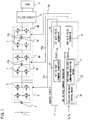
- FIG. 1 is a diagram illustrating the configuration of the power converting apparatus according to the first embodiment of this invention.
- a first smoothing capacitor 2 for smoothing a DC bus voltage is connected to a first DC power supply 1 made up of a solar battery, for example, to supply DC power to a first inverter 3 made up of a single-phase full-bridge inverter.
- a plurality (two in this case) of second inverters 4A, 4B are connected in series to an AC output line of the first inverter 3.
- the first inverter 3 which is provided with a plurality of self-turn-off semiconductor switching devices 5 (hereinafter referred to as the semiconductor switches 5) like metal oxide semiconductor field effect transistors (MOSFETs) converts DC power fed from the first smoothing capacitor 2 into AC power.
- the second inverters 4A, 4B which are provided with mutually independent second smoothing capacitors 6A, 6B and a plurality of self-turn-off semiconductor switching devices 7 (hereinafter referred to as the semiconductor switches 7) like MOSFETs convert DC power of the second smoothing capacitors 6A, 6B into AC power, respectively.
- Output voltages of the individual second inverters 4A, 4B are superimposed on an output voltage of the first inverter 3 and sine-wave AC power is applied to a load 9 through a filter circuit 8.
- voltage sensors 10a, 10b for detecting voltages V A , V B of the second smoothing capacitors 6A, 6B, respectively.
- the voltages of the second smoothing capacitors 6A, 6B are made lower than a voltage of the first smoothing capacitor 2.
- the control circuit 11 employing a processing device like a digital signal processor (DSP) or a field-programmable gate array (FPGA), for example.
- the control circuit 11 includes a first voltage command generator 12 for generating an output voltage command Vref1 for the first inverter 3, a second voltage command generator 13 which serves as voltage command generating means for generating output voltage commands VrefA, VrefB for the second inverters 4A, 4B, respectively, a first gate pulse generator 14 for generating a gate pulse 14a for controllably driving the first inverter 3 based on the output voltage command Vref1 for the first inverter 3, and a second gate pulse generator 15 for generating gate pulses 15a, 15b for controllably driving the second inverters 4A, 4B based on the output voltage commands VrefA, VrefB for the second inverters 4A, 4B, respectively.
- DSP digital signal processor
- FPGA field-programmable gate array
- the second voltage command generator 13 includes voltage balance control means 16 for detecting an imbalance between the voltages V A , V B of the second smoothing capacitors 6A, 6B obtained from the voltage sensors 10a, 10b, respectively, and performing a control calculation so as to balance the voltages V A , V B , and individual voltage command generating means 17 for generating the output voltage commands VrefA, VrefB for the second inverters 4A, 4B, respectively, based on the result of the control calculation performed by the voltage balance control means 16.
- FIG. 2 is a diagram depicting output voltage waveforms of the first and second inverters 3, 4A, 4B of the power converting apparatus.
- Designated by 20 is a sine-wave voltage output by the entire power converting apparatus to the load 9.
- the output voltage 21 of the first inverter 3 has a pulse waveform containing pulses generated at a rate of one pulse per half cycle, and the second inverters 4A, 4B output voltages 22a, 22b that would make up for a difference between the sine-wave voltage and the output voltage 21 of the first inverter 3 by a pulse width modulation (PWM) method.
- PWM pulse width modulation
- the output voltages 22a, 22b of the individual second inverters 4A, 4B are approximately equal to each other and the sum of these voltages is used to make up for the difference between the sine-wave voltage and the output voltage 21 of the first inverter 3.
- the sum of the output voltages of the series-connected first and second inverters 3, 4A, 4B is output to the load 9.
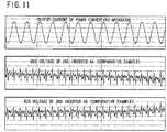
- FIG. 3 illustrates a voltage waveform of a sum voltage 22 of the output voltages 22a, 22b of the individual second inverters 4A, 4B.
- Designated by 23 is an output current waveform of the power converting apparatus.
- FIG. 4 illustrates an electric power waveform of summed power 24 of individual output power components (instantaneous values) of the second inverters 4A, 4B.
- electric power is output by the PWM method in such a manner that the amounts of positive and negative power components become equal to each other, or such that a power balance during one cycle becomes approximately zero.
- control operation performed by the control circuit 11 is described.
- the first voltage command generator 12 generates the output voltage command Vref1 so that the first inverter 3 outputs a pulse voltage containing pulses generated at a rate of one pulse per half cycle based on the sine-wave voltage which is an output target of the entire power converting apparatus and the voltage of the first smoothing capacitor 2.
- the pulse width of this pulse voltage is determined such that a power balance (summed power balance) of the second inverters 4A, 4B that output the sum voltage 22 used for making up for the difference between the sine-wave voltage and the output voltage 21 of the first inverter 3 becomes approximately zero.
- the first gate pulse generator 14 generates the gate pulse 14a for controllably driving the individual semiconductor switches 5 of the first inverter 3 based on the output voltage command Vref1.
- the second voltage command generator 13 which is provided with the voltage balance control means 16 and the individual voltage command generating means 17 individually generates the output voltage commands VrefA, VrefB for the respective second inverters 4A, 4B so that the voltages V A , V B of the second smoothing capacitors 6A, 6B are balanced.
- the second gate pulse generator 15 generates the gate pulses 15a for controllably driving the individual semiconductor switches 7 of the second inverter 4A based on the output voltage command VrefA as well as the gate pulses 15b for controllably driving the individual semiconductor switches 7 of the second inverter 4B based on the output voltage command VrefB.
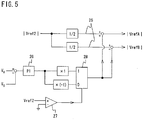
- FIG. 5 is a control block diagram of the second voltage command generator 13. It is to be noted that FIG. 5 depicts only a case where the output current 23 has a positive polarity for the sake of explanation.
- a target sum voltage Vref2 which becomes an output voltage command for the sum voltage 22 that is the sum of the output voltages of the two second inverters 4A, 4B is generated by subtracting the output voltage command Vref1 for the first inverter 3 from the sine-wave voltage. Then, a reference voltage command 25 is generated by dividing the target sum voltage Vref2 into two equal parts.
- an amount of control derived by proportional-integral (PI) control is generated by a circuit 26 so that the difference between the voltage V A of the second smoothing capacitor 6A and the voltage V B of the second smoothing capacitor 6B becomes zero and, then, positive and negative amounts of control are generated from the aforementioned amount of control and a value obtained by inverting the plus or minus sign of the amount of control.
- PI proportional-integral
- a comparator 27 detects the polarity of the target sum voltage Vref2 and a circuit 28 outputs one of the positive and negative amounts of control depending on the polarity of the target sum voltage Vref2. Then, the amount of control output from the circuit 28 is added to the reference voltage command 25 to generate one of the output voltage commands VrefA, VrefB and the amount of control is subtracted from the reference voltage command 25 to generate the other of the output voltage commands VrefA, VrefB. It is to be noted that the sum of the two output voltage commands VrefA, VrefB always coincides with the target sum voltage Vref2.
- the reference voltage command 25 and the two output voltage commands VrefA, VrefB have the same polarity, it is assumed here that the individual output voltage commands VrefA, VrefB are generated as absolute values and the reference voltage command 25 is also treated as an absolute value for the sake of simplification.
- the voltage balance control means 16 calculates the amount of control for feedback control operation in such a manner that the difference between the voltage V A of the second smoothing capacitor 6A and the voltage V B of the second smoothing capacitor 6B becomes zero as mentioned above.
- the individual voltage command generating means 17 calculates the target sum voltage Vref2 and generates the individual output voltage commands VrefA, VrefB upon making an adjustment involving addition and subtraction of the amount of control calculated by the voltage balance control means 16 to and from the reference voltage command 25 obtained by dividing the target sum voltage Vref2 into two equal parts.
- the direction of this adjustment is determined depending on whether the second smoothing capacitors 6A, 6B are in charging or discharging mode which can be known from the polarity of the target sum voltage Vref2.
- the target sum voltage Vref2 has the positive polarity and the second smoothing capacitors 6A, 6B are in the discharging mode in phases 0 - ⁇ 1, ⁇ 2 - ⁇ 3 and ⁇ 4 - ⁇ whereas the target sum voltage Vref2 has the negative polarity and the second smoothing capacitors 6A, 6B are in the charging mode in phases ⁇ 1 - ⁇ 2 and ⁇ 3 - ⁇ 4.
- the circuit 26 When the balance between the voltage V A of the second smoothing capacitor 6A and the voltage V B of the second smoothing capacitor 6B is lost, resulting in a situation expressed by V A > V B , the circuit 26 outputs a positive amount of control and the absolute value of the output voltage command VrefA is increased and the absolute value of the output voltage command VrefB is decreased so that the amount of discharging from the second smoothing capacitor 6A becomes larger than the amount of discharging from the second smoothing capacitor 6B in the case of the discharging mode.
- the absolute value of the output voltage command VrefB is increased and the absolute value of the output voltage command VrefA is decreased by inverting the plus and minus signs of the amounts of control so that the amount of charging into the second smoothing capacitor 6B becomes larger than the amount of charging into the second smoothing capacitor 6A.
- the circuit 26 When a situation expressed by V A ⁇ V B is created, on the other hand, the circuit 26 outputs a negative amount of control and the absolute value of the output voltage command VrefB is increased and the absolute value of the output voltage command VrefA is decreased so that the amount of discharging from the second smoothing capacitor 6B becomes larger than the amount of discharging from the second smoothing capacitor 6A in the case of the discharging mode.
- the output voltage command VrefA is increased and the absolute value of the output voltage command VrefB is decreased by inverting the plus and minus signs of the amounts of control so that the amount of charging into the second smoothing capacitor 6A becomes larger than the amount of charging into the second smoothing capacitor 6B.
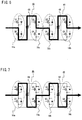
- each of the second inverters 4A, 4B is configured such that, among two arms made up of two each semiconductor switches 7 (Q1 - Q8), one is a polarity fixing arm 18a, 18b which performs switching operation only when the polarity of the output voltage changes and the other is a PWM arm 19a, 19b which forms a waveform by PWM switching operation.
- the polarity fixing arm 18a is configured with the semiconductor switches Q1, Q2 and the PWM arm 19a is configured with the semiconductor switches Q3, Q4. Also, in the second inverter 4B, the polarity fixing arm 18b is configured with the semiconductor switches Q5, Q6 and the PWM arm 19b is configured with the semiconductor switches Q7, Q8.
- the output power of the second inverters 4A, 4B has the positive polarity and the second smoothing capacitors 6A, 6B are in the discharging mode, in which case an electric current flowing through the second inverters 4A, 4B flows through a current path depicted in FIG. 6 .
- the semiconductor switches Q2, Q6 of the polarity fixing arms 18a, 18b remain constantly ON and the amount of discharging is determined by the individual duty factors of the semiconductor switches Q3, Q7 of the PWM arms 19a, 19b.
- the duty factors of the semiconductor switches Q3, Q7 are determined according to the absolute values of the individual output voltage commands VrefA, VrefB.
- the semiconductor switches Q3, Q7 one having a higher duty factor more decreases the voltages of the second smoothing capacitors 6A, 6B, more causing the DC bus voltage of each of the second inverters 4A, 4B to drop.
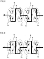
- the output power of the second inverters 4A, 4B has the negative polarity and the second smoothing capacitors 6A, 6B are in the charging mode, in which case the electric current flowing through the second inverters 4A, 4B flows through a current path depicted in FIG. 7 .
- the semiconductor switches Q1, Q5 of the polarity fixing arms 18a, 18b remain constantly ON and the amount of charging is determined by the individual duty factors of the semiconductor switches Q4, Q8 of the PWM arms 19a, 19b.
- the duty factors of the semiconductor switches Q4, Q8 are determined according to the absolute values of the individual output voltage commands VrefA, VrefB. Among the semiconductor switches Q4, Q8, one having a higher duty factor more increases the voltages of the second smoothing capacitors 6A, 6B, more causing the DC bus voltage of each of the second inverters 4A, 4B to increase.
- the output power of the second inverters 4A, 4B has the negative polarity and the second smoothing capacitors 6A, 6B are in the charging mode, in which case the electric current flowing through the second inverters 4A, 4B flows through a current path depicted in FIG. 8 .
- the semiconductor switches Q2, Q6 of the polarity fixing arms 18a, 18b remain constantly ON and the amount of charging is determined by the individual duty factors of the semiconductor switches Q3, Q7 of the PWM arms 19a, 19b.
- the duty factors of the semiconductor switches Q3, Q7 are determined according to the absolute values of the individual output voltage commands VrefA, VrefB. Among the semiconductor switches Q3, Q7, one having a higher duty factor more increases the voltages of the second smoothing capacitors 6A, 6B, more causing the DC bus voltage of each of the second inverters 4A, 4B to increase.
- the output power of the second inverters 4A, 4B has the positive polarity and the second smoothing capacitors 6A, 6B are in the discharging mode, in which case the electric current flowing through the second inverters 4A, 4B flows through a current path depicted in FIG. 9 .
- the semiconductor switches Q1, Q5 of the polarity fixing arms 18a, 18b remain constantly ON and the amount of discharging is determined by the individual duty factors of the semiconductor switches Q4, Q8 of the PWM arms 19a, 19b.
- the duty factors of the semiconductor switches Q4, Q8 are determined according to the absolute values of the individual output voltage commands VrefA, VrefB.
- the semiconductor switches Q4, Q8 one having a higher duty factor more decreases the voltages of the second smoothing capacitors 6A, 6B, more causing the DC bus voltage of each of the second inverters 4A, 4B to drop.
- the outputs of the individual second inverters 4A, 4B are controlled by the pertinent output voltage commands VrefA, VrefB in such a manner that the voltages of the two second smoothing capacitors 6A, 6B which work as the respective DC bus voltages become equal to each other. For this reason, an imbalance between the DC bus voltages of the second inverters 4A, 4B is suppressed and can be controlled to become equal to each other at a specific value as depicted in FIG. 10 .
- a comparative example is a case in which the reference voltage command 25 obtained by dividing the target sum voltage Vref2 into two equal parts is directly used as the output voltage command for the individual second inverters 4A, 4B.
- the two second inverters 4A, 4B are configured in the same fashion, the second inverters 4A, 4B have different circuit constants in actuality due to a difference in impedance between the second smoothing capacitor 6A and the second smoothing capacitor 6B, a difference in pattern between the second inverters 4A, 4B and a difference in properties of the semiconductor switches 7.
- the output voltage commands are generated upon making an adjustment so that the DC bus voltages of the individual second inverters 4A, 4B are balanced as discussed in the foregoing. For this reason, it is possible to control the DC bus voltages of the second inverters 4A, 4B to become equal to each other at a specific value without the need to control the voltages by exchanging DC power with the exterior. Therefore, reliability of output control is improved with an apparatus structure featuring a reduced cost and advanced compactness.
- the power converting apparatus may employ a different feedback control operation like proportional control or integral control, for example.
- the power converting apparatus may be configured to perform feedback control so that the difference between each of the voltages of the second smoothing capacitors 6A, 6B and a target voltage value becomes zero and then generate the output voltage commands for the individual second inverters 4A, 4B.
- the first inverter 3 is configured to output a voltage containing pulses generated at a rate of one pulse per half cycle in the foregoing embodiment, the embodiment is not limited to this configuration. Although it is desirable that the number of pulses generated be a few pulses or less per half cycle for achieving a high efficiency, a first inverter 3 configured to output more pulses is also applicable to the present embodiment.
- the power converting apparatus has the same configuration as illustrated in FIG. 1 .
- the first inverter 3 is controlled in the same fashion as in the above-described first embodiment. Specifically, the first voltage command generator 12 generates the output voltage command Vref1 so that the first inverter 3 outputs a pulse voltage containing pulses generated at a rate of one pulse per half cycle upon determining the pulse width of the pulse voltage in such a manner that a power balance (summed power balance) of the second inverters 4A, 4B becomes approximately zero. Then, the first gate pulse generator 14 generates the gate pulse 14a for controllably driving the individual semiconductor switches 5 of the first inverter 3 based on the output voltage command Vref1.
- the second voltage command generator 13 which is provided with the voltage balance control means 16 and the individual voltage command generating means 17 individually generates the output voltage commands VrefA, VrefB for the respective second inverters 4A, 4B so that the voltages V A , V B of the second smoothing capacitors 6A, 6B are balanced.
- the second gate pulse generator 15 generates the gate pulses 15a for controllably driving the individual semiconductor switches 7 of the second inverter 4A based on the output voltage command VrefA as well as the gate pulses 15b for controllably driving the individual semiconductor switches 7 of the second inverter 4B based on the output voltage command VrefB.
- the voltage balance control means 16 compares the voltage V A of the second smoothing capacitor 6A and the voltage V B of the second smoothing capacitor 6B and, when the difference therebetween exceeds a specified value, outputs a control signal which causes only one of the second inverters 4A, 4B to provide an output.
- the individual voltage command generating means 17 first generates the target sum voltage Vref2 which becomes an output voltage command for the sum voltage 22 that is the sum of the output voltages of the two second inverters 4A, 4B by subtracting the output voltage command Vref1 for the first inverter 3 from the sine-wave voltage in the same fashion as in the above-described first embodiment. Next, the individual voltage command generating means 17 generates the reference voltage command 25 by dividing the target sum voltage Vref2 into two equal parts.
- the reference voltage command 25 is used as the output voltage commands VrefA, VrefB for the respective second inverters 4A, 4B.
- the individual voltage command generating means 17 makes one of the output voltage commands VrefA, VrefB for the second inverters 4A, 4B equal to zero and the other equal to the target sum voltage Vref2.
- a decision on which output voltage command should be used as the target sum voltage Vref2 is made depending on whether the second smoothing capacitors 6A, 6B are in charging or discharging mode which can be known from the polarity of the target sum voltage Vref2.
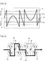
- control operation for causing only one of the second inverters 4A, 4B to output one of the output voltage commands used as the target sum voltage Vref2 can be performed only during periods when the target sum voltage Vref2 falls within a voltage range 29 in which the target sum voltage Vref2 is equal to or lower than voltage levels of the second smoothing capacitors 6A, 6B as depicted in FIG. 12 .
- the reference voltage command 25 is used as each of the output voltage commands VrefA, VrefB during periods when a situation expressed by Vref2 > V A (V B ) or Vref2 ⁇ -V A (V B ) is created.
- Described below is specific control operation performed when the balance between the voltage V A of the second smoothing capacitor 6A and the voltage V B of the second smoothing capacitor 6B is destroyed during the periods when the target sum voltage Vref2 falls within the voltage range 29, or during the periods when a situation expressed by -V A (V B ) ⁇ Vref2 ⁇ V A (V B ) is created.
- the output voltage command VrefB is made equal to the target sum voltage Vref2 and the output voltage command VrefA is made equal to zero so that only the second smoothing capacitor 6B is charged.
- This arrangement causes the voltage V A of the second smoothing capacitor 6A to drop and the voltage V B of the second smoothing capacitor 6B to rise,
- the output voltage command VrefA is made equal to the target sum voltage Vref2 and the output voltage command VrefB is made equal to zero so that only the second smoothing capacitor 6A is charged.
- This arrangement causes the voltage V A of the second smoothing capacitor 6A to rise and the voltage V B of the second smoothing capacitor 6B to drop.
- the semiconductor switches Q6, Q8 of the second inverter 4B are kept constantly ON and the semiconductor switches Q5, Q7 are kept constantly OFF in order to keep the second inverter 4B in a completely shorted state.
- the semiconductor switch Q2 of the polarity fixing arm 18a is kept constantly ON and the semiconductor switch Q3 of the PWM arm 19a is turned ON at a duty factor determined according to the absolute value of the output voltage command VrefA (Vref2).
- the output voltage commands are generated upon making an adjustment so that the DC bus voltages of the individual second inverters 4A, 4B are balanced as discussed above in this embodiment as well. Accordingly, as is the case with the first embodiment, it is possible to control the DC bus voltages of the second inverters 4A, 4B to become equal to each other at a specific value without the need to control the voltages by exchanging DC power with the exterior. Therefore, reliability of output control is improved with an apparatus structure featuring a reduced cost and advanced compactness.
- first and second embodiments are configured to each include the two second inverters, there may be provided three or more second inverters.
- FIG. 14 is a diagram illustrating the configuration of a power converting apparatus according to a third embodiment of the present invention.
- a first smoothing capacitor 2 is connected to a first DC power supply 1 to supply DC power to a first inverter 3 made up of a single-phase full-bridge inverter.
- Three second inverters 4A, 4B, 4C are connected in series to an AC output line of the first inverter 3.
- the second inverters 4A, 4B, 4C are respectively provided with mutually independent second smoothing capacitors 6A, 6B, 6C and a plurality of switching devices 7, and output voltages of the individual second inverters 4A, 4B, 4C are superimposed on an output voltage of the first inverter 3, whereby sine-wave AC power is applied to a load 9 through a filter circuit 8.
- voltage sensors 10a, 10b, 10c for detecting voltages V A , V B , V c of the second smoothing capacitors 6A, 6B, 6C, respectively.
- the control circuit 11a employing a processing device like a DSP or an FPGA, for example.
- the control circuit 11a includes a first voltage command generator 12 for generating an output voltage command Vref1 for the first inverter 3, a second voltage command generator 13 for generating output voltage commands VrefA, VrefB, VrefC for the second inverters 4A, 4B, 4C, respectively, a first gate pulse generator 14 for generating a gate pulse 14a for controllably driving the first inverter 3 based on the output voltage command Vref1 for the first inverter 3, and a second gate pulse generator 15 for generating gate pulses 15a, 15b, 15c for controllably driving the second inverters 4A, 4B, 4C based on the output voltage commands VrefA, VrefB, VrefC for the second inverters 4A, 4B, 4C, respectively.
- the first voltage command generator 12 generates the output voltage command Vref1 for the first inverter 3 in the same fashion as in the above-described first embodiment.
- the second voltage command generator 13 which is provided with voltage balance control means 16 and individual voltage command generating means 17 individually generates the output voltage commands VrefA, VrefB, VrefC for the respective second inverters 4A, 4B, 4C so that the voltages V A , V B , V c of the second smoothing capacitors 6A, 6B, 6C are balanced one another.
- the three second inverters 4 (4A, 4B, 4C) are divided into two groups one of which includes the two second inverters 4A, 4B and the other includes the remaining second inverter 4C and, based on a comparison between an average voltage of the second smoothing capacitors 6A, 6B and the voltage V C of the second smoothing capacitor 6C, the group having a higher voltage is referred to as group A in which the voltage is decreased while the group having a lower voltage is referred to as group B in which the voltage is increased.
- an average voltage is used as the voltage of the second smoothing capacitors.
- the output voltage command for each second inverter 4 in group A is so generated as to have an absolute-valued voltage lower than a reference voltage command 25a which is obtained by dividing a target sum voltage Vref2 into three equal parts and the output voltage command for each second inverter 4 in group B is so generated as to have an absolute-valued voltage higher than the reference voltage command 25a.
- the output voltage command for each second inverter 4 in group A is so generated as to have an absolute-valued voltage higher than the reference voltage command 25a and the output voltage command for each second inverter 4 in group B is so generated as to have an absolute-valued voltage lower than the reference voltage command 25a.
- FIG. 15 is a control block diagram of the second voltage command generator 13 according to the present embodiment. It is to be noted that FIG. 15 depicts only a case where an output current 23 has a positive polarity for the sake of explanation.
- the target sum voltage Vref2 which becomes an output voltage command for a sum voltage 22 that is the sum of the output voltages of the three second inverters 4A, 4B, 4C is generated by subtracting the output voltage command Vref1 for the first inverter 3 from a sine-wave voltage. Then, the reference voltage command 25a is generated by dividing the target sum voltage Vref2 into three equal parts.
- an amount of control derived by PI control is generated by a circuit 26 so that the difference between the average voltage of the voltages V A , V B of the second smoothing capacitors 6A, 6B and the voltage V C of the remaining second smoothing capacitor 6C becomes zero and, then, positive and negative amounts of control are generated from the aforementioned amount of control and a value obtained by inverting the plus or minus sign of the amount of control.
- a comparator 27 detects the polarity of the target sum voltage Vref2 and a circuit 28 outputs one of the positive and negative amounts of control depending on the polarity of the target sum voltage Vref2,
- values obtained by distributing the amount of control output from the circuit 28 according to the ratio of the voltages V A , V B are individually added to the reference voltage command 25a to generate the output voltage commands VrefA, VrefB and the amount of control is subtracted from the reference voltage command 25a to generate the output voltage command VrefC. It is to be noted that the sum of the three output voltage commands VrefA, VrefB, VrefC always coincides with the target sum voltage Vref2.
- the reference voltage command 25a and the three output voltage commands VrefA, VrefB, VrefC have the same polarity, it is assumed here that the individual output voltage commands VrefA, VrefB, VrefC are generated as absolute values and the reference voltage command 25a is also treated as an absolute value for the sake of simplification.
- the output voltage commands are generated upon making an adjustment so that the DC bus voltages of the individual second inverters 4A, 4B, 4C are balanced. For this reason, it is possible to control the DC bus voltages of the second inverters 4A, 4B, 4C to become equal to one another at a specific value without the need to control the voltages by exchanging DC power with the exterior. Therefore, reliability of output control is improved with an apparatus structure featuring a reduced cost and advanced compactness.
- the DC bus voltages of the second inverters 4 may be balanced by applying the foregoing second embodiment to a power converting apparatus provided with three or more second inverters 4, thereby creating the same advantageous effects.
- a plurality of second inverters 4 are divided into two groups and, based on a comparison between average voltages of the second smoothing capacitors 6, the group having a higher voltage is referred to as group A in which the voltage is decreased while the group having a lower voltage is referred to as group B in which the voltage is increased.
- group A the group having a higher voltage
- group B the group having a lower voltage
- the below-described control operation is performed when the difference between the average voltages exceeds a specified value.
- the output voltage command for each second inverter 4 in group A is set to 0 and the output voltage command for each second inverter 4 in group B only is generated by distributing the target sum voltage Vref2 according to the ratio of the voltages of the second smoothing capacitors 6, for example, to perform output control.
- the output voltage command for each second inverter 4 in group B is set to 0 and the output voltage command for each second inverter 4 in group A only is generated by distributing the target sum voltage Vref2 according to the ratio of the voltages of the second smoothing capacitors 6, for example, to perform output control.
- the control operation for charging or discharging the second smoothing capacitors 6 in only one of the groups is possible only during periods when the target sum voltage Vref2 becomes equal to or lower than the voltage level of the sum of the voltages of the second smoothing capacitors 6 of the aforementioned one of the groups in which output control is performed in this case as well.
- the reference voltage command 25a obtained by dividing the target sum voltage Vref2 by the number of the second inverters 4 into equal parts is used as each of the output voltage commands as is the case when the difference between the voltages of the second smoothing capacitors 6 of the different groups falls within a specified value range.
- the first inverter may be a multi-level inverter like a three-level single-phase inverter 30 as illustrated in FIG. 16 .
- two series-connected first smoothing capacitors 2a, 2b for smoothing a voltage of the DC power supply 1 are connected.
- the first inverter may be a three-phase inverter 31 as illustrated in FIG. 17 , in which case a plurality of second inverters 4A, 4B are individually connected in series to AC output lines of individual phases of the three-phase inverter 31 and the second inverters 4A, 4B of each phase are controlled in the same manner as in each of the above-described embodiments.
- the present invention can be widely applied to power converting apparatuses which convert DC power into AC power and, in particular, to those used as power conditioners, for example, which connect a photovoltaic voltage or the like to a power system.
Description
- The present invention relates to a power converting apparatus which converts DC power into AC power and, in particular, the invention is concerned with a power converting apparatus used as a power conditioner, for example, which connects a photovoltaic voltage to a power system.
- A power conditioner used as a conventional power converting apparatus is configured to obtain an output voltage from the sum of voltages generated by individual inverters with an AC side of a single-phase inverter (first inverter) whose DC source is a DC voltage obtained by boosting a photovoltaic voltage by a chopper circuit and AC sides of the other inverters (second and third inverters) connected in series, the power conditioner being capable of outputting a voltage higher than the DC voltage boosted by the chopper circuit. Also, the power conditioner is controlled such that outputs of the second and third inverters become equal to each other (refer to
Patent Document 1, for example). -
- Patent Document 1 :
- International publication No.
WO2006/090674 - IWAYA K ET AL: "High-frequency switched mode power amplifier with small capacity filter inverters", INDUSTRIAL ELECTRONICS SOCIETY, 2004. IECON 2004. 30TH ANNUAL CONFEREN CE OF IEEE BUSAN. SOUTH KOREA 2-6 NOV. 2004. PISCATAWAY. NJ. USA.IEEE. vol. 1.2 November 2004 (2004-11-02), pages 35-40.
is considered to be the closest prior art, and discloses a related power converting apparatus. - In the conventional power converting apparatus, the two inverters other than the first inverter of which input is the output DC voltage of the chopper circuit are provided with DC/DC converters serving as DC power sources to maintain DC bus voltages at a constant level. For this reason, the DC bus voltages of the two inverters are kept equal to each other and, thus, the output of the power converting apparatus is controlled with high reliability. There has however been a problem that the provision of the DC/DC converters which are hardware results in an increase in the structure of the apparatus as well as an increase in cost.
- The present invention has been made to solve the aforementioned problem. Accordingly, it is an object of the invention to suppress an imbalance of DC bus voltages of a plurality of inverters connected to a first inverter and stabilize the DC bus voltages with an inexpensive and compact apparatus structure.
- A power converting apparatus according to the present invention is given in
claims - The power converting apparatus further includes voltage command generating means for individually generating output voltage commands for the second inverters, wherein the voltage command generating means generates the output voltage commands upon individually making an adjustment so that the voltages of the individual second smoothing capacitors become equal to each other depending on whether the second smoothing capacitors are in charging or discharging mode while keeping the sum of the individual output voltage commands at a target sum voltage to be matched by the sum of the output voltages of the plurality of second inverters
- According to the present invention, the voltage command generating means generates the output voltage commands for the individual second inverters upon individually making an adjustment so that the voltages of the individual second smoothing capacitors become equal to each other depending on whether the second smoothing capacitors are in charging or discharging mode.
- Therefore, DC bus voltages of the plurality of second inverters can be stabilized with an imbalance therebetween suppressed. Also, it is not necessary to exchange DC power with the exterior, requiring no DC/DC converter or the like, and thus it is possible to provide an apparatus structure featuring a reduced cost and advanced compactness.
- It is remarked here that the claimed invention corresponds to what is called the third embodiment of the present invention in the description. The first and second embodiments of the present invention are to be considered as comparative examples.
- FIG. 1
- is a diagram illustrating the configuration of a power converting apparatus according to a first embodiment of the present invention;
- FIG. 2
- is a diagram depicting output voltage waveforms of first and second inverters according to the first embodiment of the present invention;
- FIG. 3
- is a diagram depicting a voltage waveform of a sum voltage of individual output voltages of the second inverters according to the first embodiment of the present invention;
- FIG. 4
- is a diagram depicting an electric power waveform of summed power of individual output power components (instantaneous values) of the second inverters according to the first embodiment of the present invention;
- FIG. 5
- is a control block diagram of a second voltage command generator according to the first embodiment of the present invention;
- FIG. 6
- is a diagram depicting a current path through a plurality of second inverters according to the first embodiment of the present invention;
- FIG. 7
- is a diagram depicting a current path through the plurality of second inverters according to the first embodiment of the present invention;
- FIG. 8
- is a diagram depicting a current path through the plurality of second inverters according to the first embodiment of the present invention;
- FIG. 9
- is a diagram depicting a current path through the plurality of second inverters according to the first embodiment of the present invention;
- FIG. 10
- is a diagram depicting DC bus voltages of the plurality of second inverters according to the first embodiment of the present invention;
- FIG. 11
- is a diagram depicting DC bus voltages of a plurality of second inverters according to a comparative example of the first embodiment of the present invention;
- FIG. 12
- is a diagram depicting a control range according to a second embodiment of the present invention;
- FIG. 13
- is a diagram depicting a current path through a plurality of second inverters according to the second embodiment of the present invention;
- FIG. 14
- is a diagram illustrating the configuration of a power converting apparatus according to a third embodiment of the present invention;
- FIG. 15
- is a control block diagram of a second voltage command generator according to the third embodiment of the present invention;
- FIG. 16
- is a diagram illustrating the configuration of a power converting apparatus according to an alternative example of the third embodiment of the present invention; and
- FIG. 17
- is a diagram illustrating the configuration of a power converting apparatus according to another alternative example of the third embodiment of the present invention.
- A power converting apparatus according to a first embodiment of the present invention is now described.
FIG. 1 is a diagram illustrating the configuration of the power converting apparatus according to the first embodiment of this invention. - As illustrated in
FIG. 1 , afirst smoothing capacitor 2 for smoothing a DC bus voltage is connected to a firstDC power supply 1 made up of a solar battery, for example, to supply DC power to a first inverter 3 made up of a single-phase full-bridge inverter. A plurality (two in this case) ofsecond inverters - The first inverter 3 which is provided with a plurality of self-turn-off semiconductor switching devices 5 (hereinafter referred to as the semiconductor switches 5) like metal oxide semiconductor field effect transistors (MOSFETs) converts DC power fed from the
first smoothing capacitor 2 into AC power. Thesecond inverters second smoothing capacitors second smoothing capacitors - Output voltages of the individual
second inverters load 9 through afilter circuit 8. There are also providedvoltage sensors second smoothing capacitors second smoothing capacitors first smoothing capacitor 2. - There is further provided a
control circuit 11 employing a processing device like a digital signal processor (DSP) or a field-programmable gate array (FPGA), for example. Thecontrol circuit 11 includes a firstvoltage command generator 12 for generating an output voltage command Vref1 for the first inverter 3, a secondvoltage command generator 13 which serves as voltage command generating means for generating output voltage commands VrefA, VrefB for thesecond inverters gate pulse generator 14 for generating agate pulse 14a for controllably driving the first inverter 3 based on the output voltage command Vref1 for the first inverter 3, and a secondgate pulse generator 15 for generatinggate pulses second inverters second inverters - The second
voltage command generator 13 includes voltage balance control means 16 for detecting an imbalance between the voltages VA, VB of thesecond smoothing capacitors voltage sensors second inverters - The working of the power converting apparatus configured as described above is explained hereunder.
-
FIG. 2 is a diagram depicting output voltage waveforms of the first andsecond inverters load 9. Theoutput voltage 21 of the first inverter 3 has a pulse waveform containing pulses generated at a rate of one pulse per half cycle, and thesecond inverters 4B output voltages output voltage 21 of the first inverter 3 by a pulse width modulation (PWM) method. - In this case, the
output voltages second inverters output voltage 21 of the first inverter 3. Thus, the sum of the output voltages of the series-connected first andsecond inverters load 9. -
FIG. 3 illustrates a voltage waveform of asum voltage 22 of theoutput voltages second inverters FIG. 4 illustrates an electric power waveform of summedpower 24 of individual output power components (instantaneous values) of thesecond inverters - Unlike the case of an ordinary PWM inverter which produces electric power having only a positive polarity, there exist a period during which the output power (summed power 24) of the
second inverters FIG. 4 , and the individualsecond smoothing capacitors - Then, electric power is output by the PWM method in such a manner that the amounts of positive and negative power components become equal to each other, or such that a power balance during one cycle becomes approximately zero.
- Next, control operation performed by the
control circuit 11 is described. - The first
voltage command generator 12 generates the output voltage command Vref1 so that the first inverter 3 outputs a pulse voltage containing pulses generated at a rate of one pulse per half cycle based on the sine-wave voltage which is an output target of the entire power converting apparatus and the voltage of thefirst smoothing capacitor 2. - The pulse width of this pulse voltage is determined such that a power balance (summed power balance) of the
second inverters sum voltage 22 used for making up for the difference between the sine-wave voltage and theoutput voltage 21 of the first inverter 3 becomes approximately zero. The firstgate pulse generator 14 generates thegate pulse 14a for controllably driving theindividual semiconductor switches 5 of the first inverter 3 based on the output voltage command Vref1. - The second
voltage command generator 13 which is provided with the voltage balance control means 16 and the individual voltage command generating means 17 individually generates the output voltage commands VrefA, VrefB for the respectivesecond inverters second smoothing capacitors - The second
gate pulse generator 15 generates thegate pulses 15a for controllably driving theindividual semiconductor switches 7 of thesecond inverter 4A based on the output voltage command VrefA as well as thegate pulses 15b for controllably driving theindividual semiconductor switches 7 of thesecond inverter 4B based on the output voltage command VrefB. -
FIG. 5 is a control block diagram of the secondvoltage command generator 13. It is to be noted thatFIG. 5 depicts only a case where the output current 23 has a positive polarity for the sake of explanation. - A target sum voltage Vref2 which becomes an output voltage command for the
sum voltage 22 that is the sum of the output voltages of the twosecond inverters reference voltage command 25 is generated by dividing the target sum voltage Vref2 into two equal parts. - On the other hand, an amount of control derived by proportional-integral (PI) control is generated by a
circuit 26 so that the difference between the voltage VA of thesecond smoothing capacitor 6A and the voltage VB of thesecond smoothing capacitor 6B becomes zero and, then, positive and negative amounts of control are generated from the aforementioned amount of control and a value obtained by inverting the plus or minus sign of the amount of control. - Also, a
comparator 27 detects the polarity of the target sum voltage Vref2 and acircuit 28 outputs one of the positive and negative amounts of control depending on the polarity of the target sum voltage Vref2. Then, the amount of control output from thecircuit 28 is added to thereference voltage command 25 to generate one of the output voltage commands VrefA, VrefB and the amount of control is subtracted from thereference voltage command 25 to generate the other of the output voltage commands VrefA, VrefB. It is to be noted that the sum of the two output voltage commands VrefA, VrefB always coincides with the target sum voltage Vref2. - Also, since the target sum voltage Vref2, the
reference voltage command 25 and the two output voltage commands VrefA, VrefB have the same polarity, it is assumed here that the individual output voltage commands VrefA, VrefB are generated as absolute values and thereference voltage command 25 is also treated as an absolute value for the sake of simplification. - The voltage balance control means 16 calculates the amount of control for feedback control operation in such a manner that the difference between the voltage VA of the
second smoothing capacitor 6A and the voltage VB of thesecond smoothing capacitor 6B becomes zero as mentioned above. - The individual voltage command generating means 17 calculates the target sum voltage Vref2 and generates the individual output voltage commands VrefA, VrefB upon making an adjustment involving addition and subtraction of the amount of control calculated by the voltage balance control means 16 to and from the
reference voltage command 25 obtained by dividing the target sum voltage Vref2 into two equal parts. The direction of this adjustment is determined depending on whether thesecond smoothing capacitors - When the output current 23 has the positive polarity, that is, when an output of the power converting apparatus has the positive polarity (phase 0 - π) as illustrated in
FIGS. 3 and 4 , the target sum voltage Vref2 has the positive polarity and thesecond smoothing capacitors second smoothing capacitors - When the balance between the voltage VA of the
second smoothing capacitor 6A and the voltage VB of thesecond smoothing capacitor 6B is lost, resulting in a situation expressed by VA > VB, thecircuit 26 outputs a positive amount of control and the absolute value of the output voltage command VrefA is increased and the absolute value of the output voltage command VrefB is decreased so that the amount of discharging from thesecond smoothing capacitor 6A becomes larger than the amount of discharging from thesecond smoothing capacitor 6B in the case of the discharging mode. - Also, in the case of the charging mode, the absolute value of the output voltage command VrefB is increased and the absolute value of the output voltage command VrefA is decreased by inverting the plus and minus signs of the amounts of control so that the amount of charging into the
second smoothing capacitor 6B becomes larger than the amount of charging into thesecond smoothing capacitor 6A. - When a situation expressed by VA < VB is created, on the other hand, the
circuit 26 outputs a negative amount of control and the absolute value of the output voltage command VrefB is increased and the absolute value of the output voltage command VrefA is decreased so that the amount of discharging from thesecond smoothing capacitor 6B becomes larger than the amount of discharging from thesecond smoothing capacitor 6A in the case of the discharging mode. - Also, in the case of the charging mode, the output voltage command VrefA is increased and the absolute value of the output voltage command VrefB is decreased by inverting the plus and minus signs of the amounts of control so that the amount of charging into the
second smoothing capacitor 6A becomes larger than the amount of charging into thesecond smoothing capacitor 6B. - The working of the individual
second inverters FIGS. 6 to 9 . - Here, each of the
second inverters polarity fixing arm PWM arm - In the
second inverter 4A, thepolarity fixing arm 18a is configured with the semiconductor switches Q1, Q2 and thePWM arm 19a is configured with the semiconductor switches Q3, Q4. Also, in thesecond inverter 4B, thepolarity fixing arm 18b is configured with the semiconductor switches Q5, Q6 and thePWM arm 19b is configured with the semiconductor switches Q7, Q8. - When the output of the power converting apparatus has the positive polarity and the
output voltages second inverters second inverters second smoothing capacitors second inverters FIG. 6 . - In this case, the semiconductor switches Q2, Q6 of the
polarity fixing arms PWM arms second smoothing capacitors second inverters - Next, when the output of the power converting apparatus has the positive polarity and the
output voltages second inverters second inverters second smoothing capacitors second inverters FIG. 7 . - In this case, the semiconductor switches Q1, Q5 of the
polarity fixing arms PWM arms - The duty factors of the semiconductor switches Q4, Q8 are determined according to the absolute values of the individual output voltage commands VrefA, VrefB. Among the semiconductor switches Q4, Q8, one having a higher duty factor more increases the voltages of the
second smoothing capacitors second inverters - Next, when the output of the power converting apparatus has the negative polarity and the
output voltages second inverters second inverters second smoothing capacitors second inverters FIG. 8 . - In this case, the semiconductor switches Q2, Q6 of the
polarity fixing arms PWM arms - The duty factors of the semiconductor switches Q3, Q7 are determined according to the absolute values of the individual output voltage commands VrefA, VrefB. Among the semiconductor switches Q3, Q7, one having a higher duty factor more increases the voltages of the
second smoothing capacitors second inverters - Next, when the output of the power converting apparatus has the negative polarity and the
output voltages second inverters second inverters second smoothing capacitors second inverters FIG. 9 . - In this case, the semiconductor switches Q1, Q5 of the
polarity fixing arms PWM arms second smoothing capacitors second inverters - As described above, the outputs of the individual
second inverters second smoothing capacitors second inverters FIG. 10 . - Described below as a comparative example is a case in which the
reference voltage command 25 obtained by dividing the target sum voltage Vref2 into two equal parts is directly used as the output voltage command for the individualsecond inverters second inverters second inverters second smoothing capacitor 6A and thesecond smoothing capacitor 6B, a difference in pattern between thesecond inverters - Therefore, when the two
second inverters second inverters FIG. 11 , for example. In this case, the DC bus voltage of thesecond inverter 4A, or the voltage value of thesecond smoothing capacitor 6A, decreases, while the DC bus voltage of thesecond inverter 4B, or the voltage value of thesecond smoothing capacitor 6B, increases. - In the present embodiment, the output voltage commands are generated upon making an adjustment so that the DC bus voltages of the individual
second inverters second inverters - While the feedback control operation involves PI (proportional-integral) control performed in such a manner that the difference between the voltages of the two
second smoothing capacitors - Also, the power converting apparatus may be configured to perform feedback control so that the difference between each of the voltages of the
second smoothing capacitors second inverters - Also, while the first inverter 3 is configured to output a voltage containing pulses generated at a rate of one pulse per half cycle in the foregoing embodiment, the embodiment is not limited to this configuration. Although it is desirable that the number of pulses generated be a few pulses or less per half cycle for achieving a high efficiency, a first inverter 3 configured to output more pulses is also applicable to the present embodiment.
- Described next is a power converting apparatus according to a second embodiment of the present invention. In this case, the power converting apparatus has the same configuration as illustrated in
FIG. 1 . - In control operation of this embodiment, the first inverter 3 is controlled in the same fashion as in the above-described first embodiment. Specifically, the first
voltage command generator 12 generates the output voltage command Vref1 so that the first inverter 3 outputs a pulse voltage containing pulses generated at a rate of one pulse per half cycle upon determining the pulse width of the pulse voltage in such a manner that a power balance (summed power balance) of thesecond inverters gate pulse generator 14 generates thegate pulse 14a for controllably driving theindividual semiconductor switches 5 of the first inverter 3 based on the output voltage command Vref1. - The second
voltage command generator 13 which is provided with the voltage balance control means 16 and the individual voltage command generating means 17 individually generates the output voltage commands VrefA, VrefB for the respectivesecond inverters second smoothing capacitors gate pulse generator 15 generates thegate pulses 15a for controllably driving theindividual semiconductor switches 7 of thesecond inverter 4A based on the output voltage command VrefA as well as thegate pulses 15b for controllably driving theindividual semiconductor switches 7 of thesecond inverter 4B based on the output voltage command VrefB. - In this case, the voltage balance control means 16 compares the voltage VA of the
second smoothing capacitor 6A and the voltage VB of thesecond smoothing capacitor 6B and, when the difference therebetween exceeds a specified value, outputs a control signal which causes only one of thesecond inverters - The individual voltage command generating means 17 first generates the target sum voltage Vref2 which becomes an output voltage command for the
sum voltage 22 that is the sum of the output voltages of the twosecond inverters reference voltage command 25 by dividing the target sum voltage Vref2 into two equal parts. - Then, under normal conditions where the difference between the voltage VA of the
second smoothing capacitor 6A and the voltage VB of thesecond smoothing capacitor 6B is equal to or smaller than the specified value, thereference voltage command 25 is used as the output voltage commands VrefA, VrefB for the respectivesecond inverters - Also, when the difference between the voltage VA of the
second smoothing capacitor 6A and the voltage VB of thesecond smoothing capacitor 6B exceeds the specified value, the individual voltage command generating means 17 makes one of the output voltage commands VrefA, VrefB for thesecond inverters second smoothing capacitors - It is to be noted that control operation for causing only one of the
second inverters voltage range 29 in which the target sum voltage Vref2 is equal to or lower than voltage levels of thesecond smoothing capacitors FIG. 12 . - For this reason, the
reference voltage command 25 is used as each of the output voltage commands VrefA, VrefB during periods when a situation expressed by Vref2 > VA(VB) or Vref2 < -VA(VB) is created. - Described below is specific control operation performed when the balance between the voltage VA of the
second smoothing capacitor 6A and the voltage VB of thesecond smoothing capacitor 6B is destroyed during the periods when the target sum voltage Vref2 falls within thevoltage range 29, or during the periods when a situation expressed by -VA(VB) ≤ Vref2 ≤ VA(VB) is created. - When VA > VB and the difference (VA - VB) therebetween exceeds the specified value in the case of the discharging mode, the output voltage command VrefA is made equal to the target sum voltage Vref2 and the output voltage command VrefB is made equal to zero so that only the
second smoothing capacitor 6A is discharged, - Also, in the case of the charging mode, the output voltage command VrefB is made equal to the target sum voltage Vref2 and the output voltage command VrefA is made equal to zero so that only the
second smoothing capacitor 6B is charged. This arrangement causes the voltage VA of thesecond smoothing capacitor 6A to drop and the voltage VB of thesecond smoothing capacitor 6B to rise, - When VA < VB and the difference (VB - VA) therebetween exceeds the specified value in the case of the discharging mode, the output voltage command VrefB is made equal to the target sum voltage Vref2 and the output voltage command VrefA is made equal to zero so that only the
second smoothing capacitor 6B is discharged. - Also, in the case of the charging mode, the output voltage command VrefA is made equal to the target sum voltage Vref2 and the output voltage command VrefB is made equal to zero so that only the
second smoothing capacitor 6A is charged. This arrangement causes the voltage VA of thesecond smoothing capacitor 6A to rise and the voltage VB of thesecond smoothing capacitor 6B to drop. - When causing only the
second inverter 4A to provide an output with the output voltage command VrefA made equal to the target sum voltage Vref2 under conditions where VA > VB in the case of the discharging mode, for example, an electric current flowing through thesecond inverters FIG. 13 . - In this case, the semiconductor switches Q6, Q8 of the
second inverter 4B are kept constantly ON and the semiconductor switches Q5, Q7 are kept constantly OFF in order to keep thesecond inverter 4B in a completely shorted state. Then, in thesecond inverter 4A, the semiconductor switch Q2 of thepolarity fixing arm 18a is kept constantly ON and the semiconductor switch Q3 of thePWM arm 19a is turned ON at a duty factor determined according to the absolute value of the output voltage command VrefA (Vref2). - The output voltage commands are generated upon making an adjustment so that the DC bus voltages of the individual
second inverters second inverters - While the foregoing first and second embodiments are configured to each include the two second inverters, there may be provided three or more second inverters.
-
FIG. 14 is a diagram illustrating the configuration of a power converting apparatus according to a third embodiment of the present invention. - As illustrated in
FIG. 14 , afirst smoothing capacitor 2 is connected to a firstDC power supply 1 to supply DC power to a first inverter 3 made up of a single-phase full-bridge inverter. Threesecond inverters - The
second inverters second smoothing capacitors devices 7, and output voltages of the individualsecond inverters load 9 through afilter circuit 8. There are also providedvoltage sensors second smoothing capacitors - There is further provided a
control circuit 11a employing a processing device like a DSP or an FPGA, for example. Thecontrol circuit 11a includes a firstvoltage command generator 12 for generating an output voltage command Vref1 for the first inverter 3, a secondvoltage command generator 13 for generating output voltage commands VrefA, VrefB, VrefC for thesecond inverters gate pulse generator 14 for generating agate pulse 14a for controllably driving the first inverter 3 based on the output voltage command Vref1 for the first inverter 3, and a secondgate pulse generator 15 for generatinggate pulses second inverters second inverters - The first
voltage command generator 12 generates the output voltage command Vref1 for the first inverter 3 in the same fashion as in the above-described first embodiment. - The second
voltage command generator 13 which is provided with voltage balance control means 16 and individual voltage command generating means 17 individually generates the output voltage commands VrefA, VrefB, VrefC for the respectivesecond inverters second smoothing capacitors - In this case, the three second inverters 4 (4A, 4B, 4C) are divided into two groups one of which includes the two
second inverters second smoothing capacitors second smoothing capacitor 6C, the group having a higher voltage is referred to as group A in which the voltage is decreased while the group having a lower voltage is referred to as group B in which the voltage is increased. In a case where there are a plurality of inverters in the group including the second inverter 4C, an average voltage is used as the voltage of the second smoothing capacitors. - When the second smoothing capacitors 6 (6A, 6B, 6C) are in the charging mode, the output voltage command for each second inverter 4 in group A is so generated as to have an absolute-valued voltage lower than a
reference voltage command 25a which is obtained by dividing a target sum voltage Vref2 into three equal parts and the output voltage command for each second inverter 4 in group B is so generated as to have an absolute-valued voltage higher than thereference voltage command 25a. - Also, when the
second smoothing capacitors 6 are in the discharging mode, the output voltage command for each second inverter 4 in group A is so generated as to have an absolute-valued voltage higher than thereference voltage command 25a and the output voltage command for each second inverter 4 in group B is so generated as to have an absolute-valued voltage lower than thereference voltage command 25a. -
FIG. 15 is a control block diagram of the secondvoltage command generator 13 according to the present embodiment. It is to be noted thatFIG. 15 depicts only a case where an output current 23 has a positive polarity for the sake of explanation. - The target sum voltage Vref2 which becomes an output voltage command for a
sum voltage 22 that is the sum of the output voltages of the threesecond inverters reference voltage command 25a is generated by dividing the target sum voltage Vref2 into three equal parts. - On the other hand, an amount of control derived by PI control is generated by a
circuit 26 so that the difference between the average voltage of the voltages VA, VB of thesecond smoothing capacitors second smoothing capacitor 6C becomes zero and, then, positive and negative amounts of control are generated from the aforementioned amount of control and a value obtained by inverting the plus or minus sign of the amount of control. Also, acomparator 27 detects the polarity of the target sum voltage Vref2 and acircuit 28 outputs one of the positive and negative amounts of control depending on the polarity of the target sum voltage Vref2, - Then, values obtained by distributing the amount of control output from the
circuit 28 according to the ratio of the voltages VA, VB are individually added to thereference voltage command 25a to generate the output voltage commands VrefA, VrefB and the amount of control is subtracted from thereference voltage command 25a to generate the output voltage command VrefC. It is to be noted that the sum of the three output voltage commands VrefA, VrefB, VrefC always coincides with the target sum voltage Vref2. - Also, since the target sum voltage Vref2, the
reference voltage command 25a and the three output voltage commands VrefA, VrefB, VrefC have the same polarity, it is assumed here that the individual output voltage commands VrefA, VrefB, VrefC are generated as absolute values and thereference voltage command 25a is also treated as an absolute value for the sake of simplification. - Again, it is the case in this embodiment that the output voltage commands are generated upon making an adjustment so that the DC bus voltages of the individual
second inverters second inverters - Incidentally, the DC bus voltages of the second inverters 4 may be balanced by applying the foregoing second embodiment to a power converting apparatus provided with three or more second inverters 4, thereby creating the same advantageous effects.
- Specifically, a plurality of second inverters 4 are divided into two groups and, based on a comparison between average voltages of the
second smoothing capacitors 6, the group having a higher voltage is referred to as group A in which the voltage is decreased while the group having a lower voltage is referred to as group B in which the voltage is increased. In this case, the below-described control operation is performed when the difference between the average voltages exceeds a specified value. - When the
second smoothing capacitors 6 are in the charging mode, the output voltage command for each second inverter 4 in group A is set to 0 and the output voltage command for each second inverter 4 in group B only is generated by distributing the target sum voltage Vref2 according to the ratio of the voltages of thesecond smoothing capacitors 6, for example, to perform output control. - Also, when the
second smoothing capacitors 6 are in the discharging mode, the output voltage command for each second inverter 4 in group B is set to 0 and the output voltage command for each second inverter 4 in group A only is generated by distributing the target sum voltage Vref2 according to the ratio of the voltages of thesecond smoothing capacitors 6, for example, to perform output control. - The control operation for charging or discharging the
second smoothing capacitors 6 in only one of the groups is possible only during periods when the target sum voltage Vref2 becomes equal to or lower than the voltage level of the sum of the voltages of thesecond smoothing capacitors 6 of the aforementioned one of the groups in which output control is performed in this case as well. - During periods other than the aforementioned periods, the
reference voltage command 25a obtained by dividing the target sum voltage Vref2 by the number of the second inverters 4 into equal parts is used as each of the output voltage commands as is the case when the difference between the voltages of thesecond smoothing capacitors 6 of the different groups falls within a specified value range. - Also, the first inverter may be a multi-level inverter like a three-level single-
phase inverter 30 as illustrated inFIG. 16 . In this case, two series-connected first smoothingcapacitors 2a, 2b for smoothing a voltage of theDC power supply 1 are connected. - Furthermore, the first inverter may be a three-
phase inverter 31 as illustrated inFIG. 17 , in which case a plurality ofsecond inverters phase inverter 31 and thesecond inverters - It will be appreciated from the foregoing that the present invention can be widely applied to power converting apparatuses which convert DC power into AC power and, in particular, to those used as power conditioners, for example, which connect a photovoltaic voltage or the like to a power system.
Claims (7)
- A power converting apparatus comprising a first inverter (3) which converts DC power fed from a first smoothing capacitor (2) connected to a first DC power supply (1) into AC power and a plurality of second inverters (4A, 4B, 4C) which are connected in series to an AC output line of the first inverter (3) and convert DC power fed from respective second smoothing capacitors (6A, 6B, 6C) into AC power, wherein voltages of the second smoothing capacitors (6A, 6B, 6C) are lower than a voltage of the first smoothing capacitor (2), the plurality of second inverters (4A, 4B, 4C) output voltages approximately equal to each other by performing PWM control so that an output power balance, which is a balance of positive polarity and negative polarity of summed output power of second inverters (4A, 4B, 4C) during one cycle, becomes approximately zero, and the power converting apparatus outputs the sum of an output voltage of the first inverter (3) and the output voltages of the second inverters (4A, 4B, 4C),
the power converting apparatus further comprising:voltage command generating means (13) for individually generating output voltage commands (VrefA, VrefB, VrefC) for the second inverters (4A, 4B, 4C), wherein the voltage command generating means (13) generates the output voltage commands (VrefA, VrefB, VrefC) upon individually making an adjustment so that the voltages of the individual second smoothing capacitors (6A, 6B, 6C) become equal to each other while keeping the sum of the individual output voltage commands (VrefA, VrefB, VrefC) at a target sum voltage (Vref2) to be matched by the sum of the output voltages of the plurality of second inverters (4A, 4B),wherein the voltage command generating means (13) is arranged to apply a charging mode for charging the second smoothing capacitors (6A, 6B, 6C) when the output voltages of the second inverters (4A, 4B, 4C) have different polarity than an output current of the power converting apparatus, and to apply a discharging mode for discharging the second smoothing capacitors (6A, 6B, 6C) when the output voltages of the second inverters (4A, 4B, 4C) have same polarity as the output current of the power converting apparatus, wherein the voltage command generating means (13) divides the plurality of second inverters (4A, 4B, 4C) into two groups based on a comparison of the voltages of the second smoothing capacitors (6A, 6B, 6C) to set group A in which the voltage of each pertinent one of the second smoothing capacitors (6A, 6B, 6C) is to be decreased and to set group B in which the voltage of each pertinent one of the second smoothing capacitors(6A, 6B, 6C) is to be increased, and calculates a reference voltage command (25a) for the individual second inverters (4A, 4B, 4C) by dividing the target sum voltage (Vref2) into equal parts, andwherein when the second smoothing capacitors (6A,6B,6C) are to be charged in the charging mode, the voltage command generating means (13) generates the output voltage command (VrefA, VrefB, VrefC) for each pertinent one of the second inverters (4A, 4B, 4C) of the group A to have an absolute-valued voltage lower than the reference voltage command (25a) as well as the output voltage command (VrefA, VrefB, VrefC) for each pertinent one of the second inverters (4A, 4B, 4C) of the group B to have an absolute-valued voltage higher than the reference voltage command (25a) andwhen the second smoothing capacitors (6A, 6B, 6C) are to be discharged in the discharging mode, the voltage command generating means(13) generates the output voltage command (VrefA, VrefB, VrefC) for each pertinent one of the second inverters (4A, 4B, 4C) of the group A to have an absolute-valued voltage higher than the reference voltage command (25a) as well as the output voltage command (VrefA, VrefB, VrefC) for each pertinent one of the second inverters (4A, 4B, 4C) of the group B to have an absolute-valued voltage lower than the reference voltage command (25a) - A power converting apparatus comprising a first inverter (3) which converts DC power fed from a first smoothing capacitor (2) connected to a first DC power supply (1) into AC power and a plurality of second inverters (4A, 4B, 4C) which are connected in series to an AC output line of the first inverter (3) and convert DC power fed from respective second smoothing capacitors (6A, 6B, 6C) into AC power, wherein voltages of the second smoothing capacitors (6A, 6B, 6C) are lower than a voltage of the first smoothing capacitor (2), the plurality of second inverters (4A, 4B, 4C) output voltages approximately equal to each other by performing PWM control so that an output power balance, which is a balance of positive polarity and negative polarity of summed output power of second inverters (4A, 4B, 4C) during one cycle, becomes approximately zero, and the power converting apparatus outputs the sum of an output voltage of the first inverter (3) and the output voltages of the second inverters (4A, 4B, 4C),
the power converting apparatus further comprising:voltage command generating means (13) for individually generating output voltage commands (VrefA, VrefB, VrefC) for the second inverters (4A, 4B, 4C), wherein the voltage command generating means (13) generates the output voltage commands (VrefA, VrefB, VrefC) upon individually making an adjustment so that the voltages of the individual second smoothing capacitors (6A, 6B, 6C) become equal to each other while keeping the sum of the individual output voltage commands (VrefA, VrefB, VrefC) at a target sum voltage (Vref2) to be matched by the sum of the output voltages of the plurality of second inverters (4A, 4B),wherein the voltage command generating means (13) is arranged to apply a charging mode for charging the second smoothing capacitors (6A, 6B, 6C) when the output voltages of the second inverters (4A, 4B, 4C) have different polarity than an output current of the power converting apparatus, and to apply a discharging mode for discharging the second smoothing capacitors (6A, 6B, 6C) when the output voltages of the second inverters (4A, 4B, 4C) have same polarity as the output current of the power converting apparatus,wherein the voltage command generating means (13) divides the plurality of second inverters (4A, 4B, 4C) into two groups based on a comparison of the voltages of the second smoothing capacitors (6A, 6B, 6C) to set group A in which the voltage of each pertinent one of the second smoothing capacitors (6A, 6B, 6C) is to be decreased and to set group B in which the voltage of each pertinent one of the second smoothing capacitors (6A, 6B, 6C) is to be increased, andwherein when the second smoothing capacitors (6A, 6B, 6C) are to be charged in the charging mode, the voltage command generating means (13) set the output voltage command (VrefA, VrefB, VrefC) for each pertinent one of the second inverters (4A, 4B, 4C) of the group A to zero and generates only the output voltage command (VrefA, VrefB, VrefC) for each pertinent one of the second inverters (4A, 4B, 4C) of the group B so as to charge each pertinent one of the second smoothing capacitors (6A, 6B, 6C), andwhen the second smoothing capacitors (6A, 6B, 6C) are to be discharged in the discharging mode, the voltage command generating means (13) set the output voltage command (VrefA, VrefB, VrefC) for each pertinent one of the second inverters (4A, 4B, 4C) of the group B to zero and generates only the output voltage command (VrefA, VrefB, VrefC) for each pertinent one of the second inverters (4A, 4B, 4C) of the group A so as to discharge each pertinent one of the second smoothing capacitors (6A, 6B, 6C). - The power converting apparatus according to claim 2,
wherein control operation for charging or discharging the second smoothing capacitors (6A, 6B, 6C) in only one of the groups A and B is performed only during a period when the absolute value of the target sum voltage (Vref2) is smaller than the sum of the voltages of the second smoothing capacitors (6A, 6B, 6C) of the one of the groups. - The power converting apparatus according to any one of claims 1 to 3,
wherein the first inverter (3) and the plurality of second inverters (4A, 4B, 4C) are configured with single-phase inverters. - The power converting apparatus according to claim 4,
wherein the first inverter (3) is made up of a full-bridge type or multi-level type single-phase inverter. - The power converting apparatus according to any one of claims 1 to 3, wherein the first inverter (3) is configured with a three-phase inverter, the plurality of second inverters (4A, 4B) are configured with single-phase inverters, and the plurality of second inverters (4A, 4B) are individually connected in series to AC output lines of individual phases of the first inverter (3).
- The power converting apparatus according to any one of claims 1 to 6, wherein the first DC power supply (1) is a solar battery.
Applications Claiming Priority (2)
| Application Number | Priority Date | Filing Date | Title |
|---|---|---|---|
| JP2009017719 | 2009-01-29 | ||
| PCT/JP2009/005967 WO2010086929A1 (en) | 2009-01-29 | 2009-11-10 | Power conversion device |
Publications (3)
| Publication Number | Publication Date |
|---|---|
| EP2383877A1 EP2383877A1 (en) | 2011-11-02 |
| EP2383877A4 EP2383877A4 (en) | 2014-12-24 |
| EP2383877B1 true EP2383877B1 (en) | 2018-09-05 |
Family
ID=42395199
Family Applications (1)
| Application Number | Title | Priority Date | Filing Date |
|---|---|---|---|
| EP09839121.2A Not-in-force EP2383877B1 (en) | 2009-01-29 | 2009-11-10 | Power conversion device |
Country Status (5)
| Country | Link |
|---|---|
| US (1) | US8649196B2 (en) |
| EP (1) | EP2383877B1 (en) |
| JP (1) | JP5285716B2 (en) |
| CN (1) | CN102301579B (en) |
| WO (1) | WO2010086929A1 (en) |
Families Citing this family (19)
| Publication number | Priority date | Publication date | Assignee | Title |
|---|---|---|---|---|
| JP5477237B2 (en) * | 2010-09-13 | 2014-04-23 | オムロン株式会社 | Inverter |
| JP5375781B2 (en) * | 2010-09-13 | 2013-12-25 | オムロン株式会社 | Inverter |
| JP2012065428A (en) * | 2010-09-15 | 2012-03-29 | Tabuchi Electric Co Ltd | Multilevel inverter |
| JP5734672B2 (en) * | 2011-01-12 | 2015-06-17 | 株式会社東芝 | Semiconductor power converter |
| JP5490263B2 (en) * | 2011-01-20 | 2014-05-14 | 三菱電機株式会社 | Power converter |
| JP5734083B2 (en) * | 2011-05-12 | 2015-06-10 | 三菱電機株式会社 | Power converter |
| US8766758B2 (en) * | 2011-08-18 | 2014-07-01 | Solid State Controls, LLC | High-frequency transformer |
| US9007789B2 (en) * | 2011-12-12 | 2015-04-14 | Chen Na | Electric circuit for high voltage power conversion |
| US8730696B2 (en) * | 2012-07-16 | 2014-05-20 | Delta Electronics, Inc. | Multi-level voltage converter |
| CN105393423B (en) * | 2013-06-07 | 2018-05-04 | Abb技术有限公司 | Method for the convertor device of power back-off and for controlling power inverter |
| WO2014199422A1 (en) * | 2013-06-10 | 2014-12-18 | 株式会社 日立製作所 | Power conversion device |
| CN104348342B (en) * | 2013-08-02 | 2019-05-31 | 通用电气公司 | Electrical conversion systems and method |
| CN103595285A (en) * | 2013-11-29 | 2014-02-19 | 哈尔滨工业大学 | Method and device for controlling energy balance between bridge arms of modularized multi-level converter |
| WO2015124165A1 (en) * | 2014-02-18 | 2015-08-27 | Abb Technology Ltd | Converter for an ac system |
| CN209134070U (en) * | 2015-08-07 | 2019-07-19 | 艾思玛太阳能技术股份公司 | Pole changer and the inverter for having idle power capability |
| US10020765B2 (en) | 2015-12-30 | 2018-07-10 | Mitsubishi Electric Corporation | Excitation device of AC exciter |
| US10270368B2 (en) * | 2016-12-02 | 2019-04-23 | Lawrence Livermore National Security, Llc | Bi-directional, transformerless voltage system |
| US11848600B2 (en) * | 2019-02-14 | 2023-12-19 | Mitsubishi Electric Corporation | Power conversion device with control circuit to adjust a common mode voltage of combined output voltages |
| WO2021100116A1 (en) * | 2019-11-19 | 2021-05-27 | 三菱電機株式会社 | Power conversion device |
Family Cites Families (9)
| Publication number | Priority date | Publication date | Assignee | Title |
|---|---|---|---|---|
| US6320767B1 (en) * | 1998-12-18 | 2001-11-20 | Kabushiki Kaisha Toshiba | Inverter apparatus |
| US6236580B1 (en) * | 1999-04-09 | 2001-05-22 | Robicon Corporation | Modular multi-level adjustable supply with series connected active inputs |
| JP3980515B2 (en) | 2003-04-22 | 2007-09-26 | 三菱電機株式会社 | Voltage fluctuation compensation device |
| JP4527767B2 (en) | 2005-02-25 | 2010-08-18 | 三菱電機株式会社 | Power converter |
| JP2006246676A (en) * | 2005-03-07 | 2006-09-14 | Kansai Electric Power Co Inc:The | Power conversion equipment, self-excited reactive power compensating system using this power conversion equipment, and power supply system |
| JP4824360B2 (en) * | 2005-07-29 | 2011-11-30 | 三菱電機株式会社 | Power converter |
| JP4811917B2 (en) * | 2005-12-27 | 2011-11-09 | 三菱電機株式会社 | Power converter |
| JP4365376B2 (en) * | 2006-02-14 | 2009-11-18 | 三菱電機株式会社 | Power converter |
| KR100886194B1 (en) * | 2007-06-08 | 2009-02-27 | 한국전기연구원 | Controller of double-fed induction generator |
-
2009
- 2009-11-10 US US13/145,573 patent/US8649196B2/en not_active Expired - Fee Related
- 2009-11-10 WO PCT/JP2009/005967 patent/WO2010086929A1/en active Application Filing
- 2009-11-10 JP JP2010548269A patent/JP5285716B2/en not_active Expired - Fee Related
- 2009-11-10 CN CN200980155648.3A patent/CN102301579B/en not_active Expired - Fee Related
- 2009-11-10 EP EP09839121.2A patent/EP2383877B1/en not_active Not-in-force
Non-Patent Citations (1)
| Title |
|---|
| None * |
Also Published As
| Publication number | Publication date |
|---|---|
| CN102301579B (en) | 2015-03-25 |
| JPWO2010086929A1 (en) | 2012-07-26 |
| EP2383877A1 (en) | 2011-11-02 |
| CN102301579A (en) | 2011-12-28 |
| US8649196B2 (en) | 2014-02-11 |
| WO2010086929A1 (en) | 2010-08-05 |
| JP5285716B2 (en) | 2013-09-11 |
| EP2383877A4 (en) | 2014-12-24 |
| US20110273916A1 (en) | 2011-11-10 |
Similar Documents
| Publication | Publication Date | Title |
|---|---|---|
| EP2383877B1 (en) | Power conversion device | |
| US8223517B2 (en) | Power converting apparatus with main converter and sub-converter | |
| JP4811917B2 (en) | Power converter | |
| EP3148067B1 (en) | Direct-current power transmission power conversion device and direct-current power transmission power conversion method | |
| JP3249380B2 (en) | Power converter | |
| US8154893B2 (en) | Three-phase power converting apparatus | |
| EP3208928B1 (en) | Converting device | |
| EP1455437A2 (en) | Power converter and power unit | |
| US9419542B2 (en) | Inverter device | |
| EP2357720B1 (en) | Power conversion device | |
| JP5400961B2 (en) | Power converter | |
| WO2016125682A1 (en) | Dc/dc converter | |
| JP5254922B2 (en) | Power converter | |
| WO2013054567A1 (en) | Power conversion device | |
| JP5734083B2 (en) | Power converter | |
| JP5410551B2 (en) | Power converter | |
| EP3151414A1 (en) | Control of neutral potential in npc 3-level converter | |
| JP7206491B2 (en) | Controller for direct power converter | |
| JP2022120255A (en) | Power supply system | |
| JP5400955B2 (en) | Power converter |
Legal Events
| Date | Code | Title | Description |
|---|---|---|---|
| PUAI | Public reference made under article 153(3) epc to a published international application that has entered the european phase |
Free format text: ORIGINAL CODE: 0009012 |
|
| 17P | Request for examination filed |
Effective date: 20110706 |
|
| AK | Designated contracting states |
Kind code of ref document: A1 Designated state(s): AT BE BG CH CY CZ DE DK EE ES FI FR GB GR HR HU IE IS IT LI LT LU LV MC MK MT NL NO PL PT RO SE SI SK SM TR |
|
| DAX | Request for extension of the european patent (deleted) | ||
| A4 | Supplementary search report drawn up and despatched |
Effective date: 20141126 |
|
| RIC1 | Information provided on ipc code assigned before grant |
Ipc: H02M 7/487 20070101ALI20141120BHEP Ipc: H02M 7/49 20070101ALI20141120BHEP Ipc: H02M 7/48 20070101AFI20141120BHEP |
|
| 17Q | First examination report despatched |
Effective date: 20150724 |
|
| GRAP | Despatch of communication of intention to grant a patent |
Free format text: ORIGINAL CODE: EPIDOSNIGR1 |
|
| INTG | Intention to grant announced |
Effective date: 20180314 |
|
| GRAS | Grant fee paid |
Free format text: ORIGINAL CODE: EPIDOSNIGR3 |
|
| GRAA | (expected) grant |
Free format text: ORIGINAL CODE: 0009210 |
|
| AK | Designated contracting states |
Kind code of ref document: B1 Designated state(s): AT BE BG CH CY CZ DE DK EE ES FI FR GB GR HR HU IE IS IT LI LT LU LV MC MK MT NL NO PL PT RO SE SI SK SM TR |
|
| REG | Reference to a national code |
Ref country code: GB Ref legal event code: FG4D |
|
| REG | Reference to a national code |
Ref country code: CH Ref legal event code: EP |
|
| REG | Reference to a national code |
Ref country code: AT Ref legal event code: REF Ref document number: 1039013 Country of ref document: AT Kind code of ref document: T Effective date: 20180915 |
|
| REG | Reference to a national code |
Ref country code: IE Ref legal event code: FG4D |
|
| REG | Reference to a national code |
Ref country code: DE Ref legal event code: R096 Ref document number: 602009054391 Country of ref document: DE |
|
| REG | Reference to a national code |
Ref country code: FR Ref legal event code: PLFP Year of fee payment: 10 |
|
| REG | Reference to a national code |
Ref country code: NL Ref legal event code: MP Effective date: 20180905 |
|
| REG | Reference to a national code |
Ref country code: LT Ref legal event code: MG4D |
|
| PG25 | Lapsed in a contracting state [announced via postgrant information from national office to epo] |
Ref country code: GR Free format text: LAPSE BECAUSE OF FAILURE TO SUBMIT A TRANSLATION OF THE DESCRIPTION OR TO PAY THE FEE WITHIN THE PRESCRIBED TIME-LIMIT Effective date: 20181206 Ref country code: BG Free format text: LAPSE BECAUSE OF FAILURE TO SUBMIT A TRANSLATION OF THE DESCRIPTION OR TO PAY THE FEE WITHIN THE PRESCRIBED TIME-LIMIT Effective date: 20181205 Ref country code: NO Free format text: LAPSE BECAUSE OF FAILURE TO SUBMIT A TRANSLATION OF THE DESCRIPTION OR TO PAY THE FEE WITHIN THE PRESCRIBED TIME-LIMIT Effective date: 20181205 Ref country code: LT Free format text: LAPSE BECAUSE OF FAILURE TO SUBMIT A TRANSLATION OF THE DESCRIPTION OR TO PAY THE FEE WITHIN THE PRESCRIBED TIME-LIMIT Effective date: 20180905 Ref country code: FI Free format text: LAPSE BECAUSE OF FAILURE TO SUBMIT A TRANSLATION OF THE DESCRIPTION OR TO PAY THE FEE WITHIN THE PRESCRIBED TIME-LIMIT Effective date: 20180905 Ref country code: SE Free format text: LAPSE BECAUSE OF FAILURE TO SUBMIT A TRANSLATION OF THE DESCRIPTION OR TO PAY THE FEE WITHIN THE PRESCRIBED TIME-LIMIT Effective date: 20180905 |
|
| REG | Reference to a national code |
Ref country code: AT Ref legal event code: MK05 Ref document number: 1039013 Country of ref document: AT Kind code of ref document: T Effective date: 20180905 |
|
| PG25 | Lapsed in a contracting state [announced via postgrant information from national office to epo] |
Ref country code: LV Free format text: LAPSE BECAUSE OF FAILURE TO SUBMIT A TRANSLATION OF THE DESCRIPTION OR TO PAY THE FEE WITHIN THE PRESCRIBED TIME-LIMIT Effective date: 20180905 Ref country code: HR Free format text: LAPSE BECAUSE OF FAILURE TO SUBMIT A TRANSLATION OF THE DESCRIPTION OR TO PAY THE FEE WITHIN THE PRESCRIBED TIME-LIMIT Effective date: 20180905 Ref country code: ES Free format text: LAPSE BECAUSE OF FAILURE TO SUBMIT A TRANSLATION OF THE DESCRIPTION OR TO PAY THE FEE WITHIN THE PRESCRIBED TIME-LIMIT Effective date: 20180905 |
|
| PG25 | Lapsed in a contracting state [announced via postgrant information from national office to epo] |
Ref country code: EE Free format text: LAPSE BECAUSE OF FAILURE TO SUBMIT A TRANSLATION OF THE DESCRIPTION OR TO PAY THE FEE WITHIN THE PRESCRIBED TIME-LIMIT Effective date: 20180905 Ref country code: PL Free format text: LAPSE BECAUSE OF FAILURE TO SUBMIT A TRANSLATION OF THE DESCRIPTION OR TO PAY THE FEE WITHIN THE PRESCRIBED TIME-LIMIT Effective date: 20180905 Ref country code: IS Free format text: LAPSE BECAUSE OF FAILURE TO SUBMIT A TRANSLATION OF THE DESCRIPTION OR TO PAY THE FEE WITHIN THE PRESCRIBED TIME-LIMIT Effective date: 20190105 Ref country code: CZ Free format text: LAPSE BECAUSE OF FAILURE TO SUBMIT A TRANSLATION OF THE DESCRIPTION OR TO PAY THE FEE WITHIN THE PRESCRIBED TIME-LIMIT Effective date: 20180905 Ref country code: RO Free format text: LAPSE BECAUSE OF FAILURE TO SUBMIT A TRANSLATION OF THE DESCRIPTION OR TO PAY THE FEE WITHIN THE PRESCRIBED TIME-LIMIT Effective date: 20180905 Ref country code: IT Free format text: LAPSE BECAUSE OF FAILURE TO SUBMIT A TRANSLATION OF THE DESCRIPTION OR TO PAY THE FEE WITHIN THE PRESCRIBED TIME-LIMIT Effective date: 20180905 Ref country code: NL Free format text: LAPSE BECAUSE OF FAILURE TO SUBMIT A TRANSLATION OF THE DESCRIPTION OR TO PAY THE FEE WITHIN THE PRESCRIBED TIME-LIMIT Effective date: 20180905 Ref country code: AT Free format text: LAPSE BECAUSE OF FAILURE TO SUBMIT A TRANSLATION OF THE DESCRIPTION OR TO PAY THE FEE WITHIN THE PRESCRIBED TIME-LIMIT Effective date: 20180905 |
|
| PG25 | Lapsed in a contracting state [announced via postgrant information from national office to epo] |
Ref country code: SK Free format text: LAPSE BECAUSE OF FAILURE TO SUBMIT A TRANSLATION OF THE DESCRIPTION OR TO PAY THE FEE WITHIN THE PRESCRIBED TIME-LIMIT Effective date: 20180905 Ref country code: SM Free format text: LAPSE BECAUSE OF FAILURE TO SUBMIT A TRANSLATION OF THE DESCRIPTION OR TO PAY THE FEE WITHIN THE PRESCRIBED TIME-LIMIT Effective date: 20180905 Ref country code: PT Free format text: LAPSE BECAUSE OF FAILURE TO SUBMIT A TRANSLATION OF THE DESCRIPTION OR TO PAY THE FEE WITHIN THE PRESCRIBED TIME-LIMIT Effective date: 20190105 |
|
| REG | Reference to a national code |
Ref country code: DE Ref legal event code: R119 Ref document number: 602009054391 Country of ref document: DE |
|
| REG | Reference to a national code |
Ref country code: CH Ref legal event code: PL |
|
| PLBE | No opposition filed within time limit |
Free format text: ORIGINAL CODE: 0009261 |
|
| STAA | Information on the status of an ep patent application or granted ep patent |
Free format text: STATUS: NO OPPOSITION FILED WITHIN TIME LIMIT |
|
| PG25 | Lapsed in a contracting state [announced via postgrant information from national office to epo] |
Ref country code: DK Free format text: LAPSE BECAUSE OF FAILURE TO SUBMIT A TRANSLATION OF THE DESCRIPTION OR TO PAY THE FEE WITHIN THE PRESCRIBED TIME-LIMIT Effective date: 20180905 Ref country code: LU Free format text: LAPSE BECAUSE OF NON-PAYMENT OF DUE FEES Effective date: 20181110 Ref country code: MC Free format text: LAPSE BECAUSE OF FAILURE TO SUBMIT A TRANSLATION OF THE DESCRIPTION OR TO PAY THE FEE WITHIN THE PRESCRIBED TIME-LIMIT Effective date: 20180905 |
|
| 26N | No opposition filed |
Effective date: 20190606 |
|
| REG | Reference to a national code |
Ref country code: BE Ref legal event code: MM Effective date: 20181130 |
|
| REG | Reference to a national code |
Ref country code: IE Ref legal event code: MM4A |
|
| GBPC | Gb: european patent ceased through non-payment of renewal fee |
Effective date: 20181205 |
|
| PG25 | Lapsed in a contracting state [announced via postgrant information from national office to epo] |
Ref country code: CH Free format text: LAPSE BECAUSE OF NON-PAYMENT OF DUE FEES Effective date: 20181130 Ref country code: SI Free format text: LAPSE BECAUSE OF FAILURE TO SUBMIT A TRANSLATION OF THE DESCRIPTION OR TO PAY THE FEE WITHIN THE PRESCRIBED TIME-LIMIT Effective date: 20180905 Ref country code: LI Free format text: LAPSE BECAUSE OF NON-PAYMENT OF DUE FEES Effective date: 20181130 |
|
| PG25 | Lapsed in a contracting state [announced via postgrant information from national office to epo] |
Ref country code: IE Free format text: LAPSE BECAUSE OF NON-PAYMENT OF DUE FEES Effective date: 20181110 Ref country code: DE Free format text: LAPSE BECAUSE OF NON-PAYMENT OF DUE FEES Effective date: 20190601 |
|
| PG25 | Lapsed in a contracting state [announced via postgrant information from national office to epo] |
Ref country code: BE Free format text: LAPSE BECAUSE OF NON-PAYMENT OF DUE FEES Effective date: 20181130 |
|
| PG25 | Lapsed in a contracting state [announced via postgrant information from national office to epo] |
Ref country code: GB Free format text: LAPSE BECAUSE OF NON-PAYMENT OF DUE FEES Effective date: 20181205 |
|
| PG25 | Lapsed in a contracting state [announced via postgrant information from national office to epo] |
Ref country code: MT Free format text: LAPSE BECAUSE OF NON-PAYMENT OF DUE FEES Effective date: 20181110 |
|
| PGFP | Annual fee paid to national office [announced via postgrant information from national office to epo] |
Ref country code: FR Payment date: 20191015 Year of fee payment: 11 |
|
| PG25 | Lapsed in a contracting state [announced via postgrant information from national office to epo] |
Ref country code: TR Free format text: LAPSE BECAUSE OF FAILURE TO SUBMIT A TRANSLATION OF THE DESCRIPTION OR TO PAY THE FEE WITHIN THE PRESCRIBED TIME-LIMIT Effective date: 20180905 |
|
| PG25 | Lapsed in a contracting state [announced via postgrant information from national office to epo] |
Ref country code: CY Free format text: LAPSE BECAUSE OF FAILURE TO SUBMIT A TRANSLATION OF THE DESCRIPTION OR TO PAY THE FEE WITHIN THE PRESCRIBED TIME-LIMIT Effective date: 20180905 Ref country code: HU Free format text: LAPSE BECAUSE OF FAILURE TO SUBMIT A TRANSLATION OF THE DESCRIPTION OR TO PAY THE FEE WITHIN THE PRESCRIBED TIME-LIMIT; INVALID AB INITIO Effective date: 20091110 Ref country code: MK Free format text: LAPSE BECAUSE OF NON-PAYMENT OF DUE FEES Effective date: 20180905 |
|
| PG25 | Lapsed in a contracting state [announced via postgrant information from national office to epo] |
Ref country code: FR Free format text: LAPSE BECAUSE OF NON-PAYMENT OF DUE FEES Effective date: 20201130 |