EP2383775B1 - Verfahren zum Erhalten einer AlN-Schicht mit deutlich vertikalen Flanken - Google Patents
Verfahren zum Erhalten einer AlN-Schicht mit deutlich vertikalen Flanken Download PDFInfo
- Publication number
- EP2383775B1 EP2383775B1 EP11163944.9A EP11163944A EP2383775B1 EP 2383775 B1 EP2383775 B1 EP 2383775B1 EP 11163944 A EP11163944 A EP 11163944A EP 2383775 B1 EP2383775 B1 EP 2383775B1
- Authority
- EP
- European Patent Office
- Prior art keywords
- layer
- substrate
- aln
- mask
- etching
- Prior art date
- Legal status (The legal status is an assumption and is not a legal conclusion. Google has not performed a legal analysis and makes no representation as to the accuracy of the status listed.)
- Active
Links
- 239000000758 substrate Substances 0.000 claims description 56
- 238000000034 method Methods 0.000 claims description 33
- 238000005530 etching Methods 0.000 claims description 32
- BASFCYQUMIYNBI-UHFFFAOYSA-N platinum Chemical compound [Pt] BASFCYQUMIYNBI-UHFFFAOYSA-N 0.000 claims description 22
- 238000000151 deposition Methods 0.000 claims description 15
- 239000000463 material Substances 0.000 claims description 15
- ZOKXTWBITQBERF-UHFFFAOYSA-N Molybdenum Chemical compound [Mo] ZOKXTWBITQBERF-UHFFFAOYSA-N 0.000 claims description 10
- 230000008021 deposition Effects 0.000 claims description 9
- 229910052750 molybdenum Inorganic materials 0.000 claims description 8
- 239000011733 molybdenum Substances 0.000 claims description 8
- VYPSYNLAJGMNEJ-UHFFFAOYSA-N Silicium dioxide Chemical compound O=[Si]=O VYPSYNLAJGMNEJ-UHFFFAOYSA-N 0.000 claims description 7
- 230000015572 biosynthetic process Effects 0.000 claims description 6
- 229910052697 platinum Inorganic materials 0.000 claims description 6
- 238000004519 manufacturing process Methods 0.000 claims description 5
- 239000004840 adhesive resin Substances 0.000 claims 1
- 229920006223 adhesive resin Polymers 0.000 claims 1
- 229910052581 Si3N4 Inorganic materials 0.000 description 10
- HQVNEWCFYHHQES-UHFFFAOYSA-N silicon nitride Chemical compound N12[Si]34N5[Si]62N3[Si]51N64 HQVNEWCFYHHQES-UHFFFAOYSA-N 0.000 description 10
- XUIMIQQOPSSXEZ-UHFFFAOYSA-N Silicon Chemical compound [Si] XUIMIQQOPSSXEZ-UHFFFAOYSA-N 0.000 description 6
- 239000010936 titanium Substances 0.000 description 5
- 229910052710 silicon Inorganic materials 0.000 description 4
- 239000010703 silicon Substances 0.000 description 4
- 229910004298 SiO 2 Inorganic materials 0.000 description 3
- RTAQQCXQSZGOHL-UHFFFAOYSA-N Titanium Chemical compound [Ti] RTAQQCXQSZGOHL-UHFFFAOYSA-N 0.000 description 3
- 230000035784 germination Effects 0.000 description 3
- 238000005240 physical vapour deposition Methods 0.000 description 3
- 238000001039 wet etching Methods 0.000 description 3
- 229940082150 encore Drugs 0.000 description 2
- 229910052594 sapphire Inorganic materials 0.000 description 2
- 239000010980 sapphire Substances 0.000 description 2
- 239000000377 silicon dioxide Substances 0.000 description 2
- 229910052719 titanium Inorganic materials 0.000 description 2
- NBIIXXVUZAFLBC-UHFFFAOYSA-N Phosphoric acid Chemical compound OP(O)(O)=O NBIIXXVUZAFLBC-UHFFFAOYSA-N 0.000 description 1
- 230000001464 adherent effect Effects 0.000 description 1
- 229910052681 coesite Inorganic materials 0.000 description 1
- PMHQVHHXPFUNSP-UHFFFAOYSA-M copper(1+);methylsulfanylmethane;bromide Chemical compound Br[Cu].CSC PMHQVHHXPFUNSP-UHFFFAOYSA-M 0.000 description 1
- 229910052906 cristobalite Inorganic materials 0.000 description 1
- 238000001514 detection method Methods 0.000 description 1
- 238000001312 dry etching Methods 0.000 description 1
- 230000001747 exhibiting effect Effects 0.000 description 1
- 230000003071 parasitic effect Effects 0.000 description 1
- 238000002360 preparation method Methods 0.000 description 1
- 239000011347 resin Substances 0.000 description 1
- 229920005989 resin Polymers 0.000 description 1
- 235000012239 silicon dioxide Nutrition 0.000 description 1
- 229910052814 silicon oxide Inorganic materials 0.000 description 1
- 229910052682 stishovite Inorganic materials 0.000 description 1
- 229910052905 tridymite Inorganic materials 0.000 description 1
Images


Classifications
-
- H—ELECTRICITY
- H01—ELECTRIC ELEMENTS
- H01L—SEMICONDUCTOR DEVICES NOT COVERED BY CLASS H10
- H01L21/00—Processes or apparatus adapted for the manufacture or treatment of semiconductor or solid state devices or of parts thereof
- H01L21/02—Manufacture or treatment of semiconductor devices or of parts thereof
- H01L21/04—Manufacture or treatment of semiconductor devices or of parts thereof the devices having potential barriers, e.g. a PN junction, depletion layer or carrier concentration layer
- H01L21/18—Manufacture or treatment of semiconductor devices or of parts thereof the devices having potential barriers, e.g. a PN junction, depletion layer or carrier concentration layer the devices having semiconductor bodies comprising elements of Group IV of the Periodic Table or AIIIBV compounds with or without impurities, e.g. doping materials
- H01L21/30—Treatment of semiconductor bodies using processes or apparatus not provided for in groups H01L21/20 - H01L21/26
- H01L21/31—Treatment of semiconductor bodies using processes or apparatus not provided for in groups H01L21/20 - H01L21/26 to form insulating layers thereon, e.g. for masking or by using photolithographic techniques; After treatment of these layers; Selection of materials for these layers
- H01L21/3105—After-treatment
- H01L21/311—Etching the insulating layers by chemical or physical means
- H01L21/31105—Etching inorganic layers
- H01L21/31111—Etching inorganic layers by chemical means
- H01L21/31116—Etching inorganic layers by chemical means by dry-etching
- H01L21/31122—Etching inorganic layers by chemical means by dry-etching of layers not containing Si, e.g. PZT, Al2O3
-
- H—ELECTRICITY
- H01—ELECTRIC ELEMENTS
- H01L—SEMICONDUCTOR DEVICES NOT COVERED BY CLASS H10
- H01L21/00—Processes or apparatus adapted for the manufacture or treatment of semiconductor or solid state devices or of parts thereof
- H01L21/02—Manufacture or treatment of semiconductor devices or of parts thereof
- H01L21/04—Manufacture or treatment of semiconductor devices or of parts thereof the devices having potential barriers, e.g. a PN junction, depletion layer or carrier concentration layer
- H01L21/18—Manufacture or treatment of semiconductor devices or of parts thereof the devices having potential barriers, e.g. a PN junction, depletion layer or carrier concentration layer the devices having semiconductor bodies comprising elements of Group IV of the Periodic Table or AIIIBV compounds with or without impurities, e.g. doping materials
- H01L21/30—Treatment of semiconductor bodies using processes or apparatus not provided for in groups H01L21/20 - H01L21/26
- H01L21/31—Treatment of semiconductor bodies using processes or apparatus not provided for in groups H01L21/20 - H01L21/26 to form insulating layers thereon, e.g. for masking or by using photolithographic techniques; After treatment of these layers; Selection of materials for these layers
- H01L21/3105—After-treatment
- H01L21/311—Etching the insulating layers by chemical or physical means
- H01L21/31105—Etching inorganic layers
-
- H—ELECTRICITY
- H10—SEMICONDUCTOR DEVICES; ELECTRIC SOLID-STATE DEVICES NOT OTHERWISE PROVIDED FOR
- H10N—ELECTRIC SOLID-STATE DEVICES NOT OTHERWISE PROVIDED FOR
- H10N30/00—Piezoelectric or electrostrictive devices
- H10N30/01—Manufacture or treatment
- H10N30/07—Forming of piezoelectric or electrostrictive parts or bodies on an electrical element or another base
- H10N30/074—Forming of piezoelectric or electrostrictive parts or bodies on an electrical element or another base by depositing piezoelectric or electrostrictive layers, e.g. aerosol or screen printing
- H10N30/076—Forming of piezoelectric or electrostrictive parts or bodies on an electrical element or another base by depositing piezoelectric or electrostrictive layers, e.g. aerosol or screen printing by vapour phase deposition
-
- H—ELECTRICITY
- H10—SEMICONDUCTOR DEVICES; ELECTRIC SOLID-STATE DEVICES NOT OTHERWISE PROVIDED FOR
- H10N—ELECTRIC SOLID-STATE DEVICES NOT OTHERWISE PROVIDED FOR
- H10N30/00—Piezoelectric or electrostrictive devices
- H10N30/01—Manufacture or treatment
- H10N30/08—Shaping or machining of piezoelectric or electrostrictive bodies
- H10N30/082—Shaping or machining of piezoelectric or electrostrictive bodies by etching, e.g. lithography
Definitions
- the invention relates to techniques for etching a material such as AlN, with a view to producing a layer of this material with one or more straight flanks, that is to say substantially perpendicular to a surface on which this layer is deposited or formed.
- substantially perpendicular means that the flank makes with said surface an angle greater than or equal to 75 °.
- This type of material is used in the production of MEMS components, for example of the type requiring a piezoelectric or dielectric layer with straight flanks.
- Such a resonator comprises a piezoelectric layer which must have one or vertical flanks, in order to prevent the propagation of parasitic waves.
- this type of material is also used in the realization of capacitive detection MEMS, which require fine and vertical "gap", or in the production of gyroscopes.
- Dry or wet etching techniques all have an isotropic character. They result in one or flanks not having the character of verticality desired: the material is indeed etched in a vertical direction, but also in a horizontal direction.
- the invention firstly relates to a method of producing an AlN layer with at least one substantially vertical or perpendicular flank with respect to a surface of a substrate, according to claim 1.
- the walk pattern defines a raised portion of the pattern relative to a lower level.
- Deposition of the AlN layer is performed on the raised portion and on the lower level.
- substantially perpendicular vertical means that the flank makes with said surface an angle greater than or equal to 75 °.
- Such a method may comprise a preliminary step of forming the topology of the substrate, by etching the surface of the substrate, so as to obtain at least the step type pattern.
- the step may have at least one lateral flank forming an angle at most equal to 15 ° relative to the perpendicular to the surface of the substrate in or on which it is made.
- the substrate comprises an underlayer, a surface of which forms, with the surface of the substrate, the walk-type pattern.
- This underlayer can be obtained by depositing a uniform layer of material, then etching at least this layer, to obtain the walk-type pattern.
- At least a portion of the underlayer and / or at least a portion of the mask layer may form an electrode.
- a method according to the invention may further comprise producing an inclined flank by etching the AlN layer.
- the etching of the AlN layer is of wet etching type.
- a method according to the invention may also make it possible to produce at least one hole with vertical edges, the diameter of the hole and the thickness of the AlN layer preferably having a diameter / thickness ratio of less than 0.5.
- the topology can result from an etching of the surface of the substrate so as to obtain at least the step type pattern.
- the step may have at least one lateral flank forming an angle at most equal to 15 ° relative to the perpendicular to the surface of the substrate in or on which it is made.
- the substrate may comprise an underlayer, a surface of which forms, with the surface of the substrate, the walk-type pattern.
- the sub-layer may be formed at least in part on a layer forming a surface topology of the support substrate.
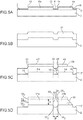
- a layer 4 which can be continuous or connected but which is not necessarily: in the example of the Figure 1A this layer comprises a first part 4 which is separated from a second part 4 'by an opening 6 which reveals the surface 2' of the substrate 2.
- This opening is for example obtained by etching a continuous initial layer of the material of the parts 4,4 ', etching which stops on the surface 2' of the substrate 2.
- the references 12 and 14 designate the flanks respectively of the portions 4 ' and 4 of this layer, on both sides of the opening 6. Two other flanks are designated by the references 10 and 12, to the left and to the right of the Figure 1A .
- this layer 4, 4 ', as well as the topology 4a, 4'a, 4b formed in the embodiments of the Figures 5A-5D and 6A-6D is lined or surrounded by a surface 2 'of the substrate located at a lower level than the upper level or the raised portion of the layer 4, 4' or topology 4a, 4'a, 4b.
- flanks 10, 12, 14, 16 are straight, that is to say substantially perpendicular to the surface 2 'of the substrate 2 or form with the perpendicular to this surface an angle less than or equal to 15 °.
- the material of the layer 4, 4 ' is, for example, titanium (Ti) or silicon (Si), or molybdenum (Mo), or platinum (Pt), or silicon nitride (SiN or Si 3 N 4 ) or silicon oxide (SiO 2 ).
- This layer 4, 4 ' may have a thickness of the order of 200 nm, or, more generally, between 10 nm and 1 ⁇ m or between 100 nm and 300 nm.
- a layer 7 of texturing or germination which will help to orient the material 31 which will then be deposited, may have been previously formed on the surface of the substrate 2.
- a layer 31 of AlN for example of approximately thickness equal to 1 micron or, more generally, between 10 nm and 5 microns.
- a deposition technique that can be used is the PVD (Physical Vapor Deposition) technique.
- This layer 31 is uniformly deposited on the portions 4, 4 'of the previously obtained layer (also known as the underlayer or topology layer), as well as on the parts of the surface 2' of the substrate 2 which are exposed, or again at the same time on the lower level defined by the layer 4, 4 'on the surface 2' and on the upper level or on the raised part of the layer 4, 4 '(or of the topology 4a, 4'a, 4b in others Figures 5A - 6D ).
- the portions 4, 4 'of the previously obtained layer also known as the underlayer or topology layer
- edges 20, 22, 24 define with, respectively, each of the edges 10, 12, 14 of the layer 4, 4 'a plane which is substantially perpendicular to the surface 2' of the substrate 2.
- this plane may not be strictly perpendicular to the surface 2 ', but be slightly inclined relative to the perpendicular direction, for example an angle between 0 ° and 15 °.
- This mask layer 40, 40 ' has a thickness which may be for example between 10 nm and 10 ⁇ m. It can be by example molybdenum Mo or silicon nitride (SiN, Si 3 N 4 ).
- the alignment of the edges 20, 22, 24 with, respectively, each of the edges 10, 12, 14 can be obtained with an accuracy of the order of 1 ⁇ m or less than 1 ⁇ m, for example an accuracy of ⁇ 1 ⁇ m on a stepper 1X, ⁇ 150 nm for deep UV lithographs (called “deep uv”) and ⁇ 50 nm for "ebeam” type lithographs.
- This alignment will make it possible to define a high end 30 1 , 32 1 , 34 1 and a low end 30 2 , 32 2 , 34 2 of the flanks 30, 32, 34 which will be made in the layer 31.
- edges of the mask 40, 40 ' will define the upper ends 30 1 , 32 1 , 34 1 of the sidewalls to be engraved (in other words, these high ends are positioned where the edges of the mask are positioned).
- edges of the layer 4, 4 ' will define the lower ends 2 , 32 2 , 34 2 of the flanks to be etched (in other words, these low ends are positioned where the edges of this layer are positioned).
- one of the flanks of the mask 40 here the right flank 26, is not aligned with the right flank 16 of the underlayer 4.
- An etching step is then performed, as shown in FIG. figure 1D .
- This step will make it possible to etch the layer 31 of AlN material, in areas that are not protected by the mask 40, 40 '.
- This etching is continued to the surface 2 'of substrate 2, this surface 2 'reappears therefore after the etching is complete.
- each flank which extends between a high end 30 1 , 32 1 , 34 1 and a low end 30 2 , 32 2 , 34 2 and is defined by the corresponding pair of high and low end 30 1 , 32 1 , 34 1 and 30 2 , 32 2 , 34 2 .
- the etching leads to the formation of a hole 60 between two portions 31a, 31b of AIN which are located under the portions 40, 40 'of hard mask.
- this hole is the flanks 32, 34 which, as indicated above, are perpendicular to the surface 2 'of the layer 2.
- the right flank 26 of the mask layer 40 is not aligned with the right flank 16 of the growth layer 4.
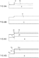
- a layer 3 is first formed, of thickness e, with a view to creating a topology in the future underlayer 4 (or, where again, topology layer).
- This layer 3 may for example be a layer for defining an electrode. It is for example SiO 2 or SiN or molybdenum (Mo) or platinum (Pt). Its thickness e is for example between 10 nm and 1 micron, or between 100 nm and 300 nm.
- a layer 4 is then deposited, the nature and thickness of which may be those already mentioned for the first embodiment.
- a layer 4 is obtained, part of which rests directly on the surface 2 'of the substrate 2, and of which another part rests on the surface 3' of the layer 3.
- the edges 13a, 13b of the layer 3 are reflected in the deposited layer 4 by flanks 10a, 10b which can be slightly inclined relative to a direction perpendicular to the surface 2 '.
- This aspect is represented in more detail in figure 3 , where it can be seen that the flank 10a defines, with a horizontal plane (reference is taken here as the surface 3 'of the layer 3), an angle ⁇ which can be of the order of 80 ° or more.
- the layer 4 has generated a step in the layer 4, of height substantially equal to the thickness e of the layer 3.
- the edges of this step are not necessarily strictly perpendicular to the surface 2 'of the substrate 2.
- the step is defined by both the lower level defined by the upper surface of the layer 4, in the areas where there is no underlying pattern 3, and the upper level or the raised portion of the same layer 4.
- a mask layer 40 is formed again, whose flanks 20, 22 are aligned - in the sense and in the manner already explained above - with the flanks 13a, 13b of the layer 3 and the flanks 10a, 10b of layer 4. This alignment will make it possible to define a high end 30 1 , 32 1 and a low end 30 2 , 32 2 of the flanks 30, 32 which will be made in the layer 31.
- edges of the mask 40 will define the upper ends 30 1 , 32 1 of the flanks to be engraved (in other words, these high ends are positioned where the edges of the mask are positioned).
- edges of the raised portion of the layer 4 will define the lower ends 2 , 32 2 of the flanks to be engraved (that is, these low ends are positioned where the edges of the raised portion of this layer are positioned) .
- This mask layer may form one or more electrodes.
- each flank which extends between a high end 30 1 , 32 1 and a low end 30 2 , 32 2 is defined by the corresponding pair of high and low end 30 1 , 32 1 and 2 , 32 2 .
- the thicknesses and materials for the layers 4, 31, 40 may be identical or similar to the thicknesses and materials indicated above, in the context of the first embodiment.
- the layer 3 it may be for example silicon dioxide (SiO 2 ), or silicon nitride (SiN), or molybdenum (Mo), or platinum (Pt) and have a thickness that can be understood as the underlayer 4, between 10 nm and 1 ⁇ m.
- the underlayer 4 is not necessarily engraved, but a topology, or step, or relief is created on the surface of this underlayer 4 by the formation, previously, of a layer underlying 3 presenting flanks which will result, during the deposition of the underlayer 4, also by flanks 10a, 10b.
- the etching of the layer 31 is then carried out in the areas not situated under the layer 40 of the mask. As before, the layer 31 is etched over its entire thickness, but the surface 4 'of the underlayer 4 is then updated.
- a portion 31a is thus obtained in AlN, with side flanks 30, 32, which are again found to be perpendicular to the horizontal surface defined here by the upper surface 4 'of the underlayer 4.
- the layer 3 it is possible to use the layer 3 to form a topology or a relief in the underlayer 4 whose edges 10a, 10b, in turn, allow to align the edges of the mask layer 40 and to define the areas in which vertical sides of the layer 31 will be obtained, after etching.
- this second embodiment it is also possible to make one or more holes such as the hole 60 of the figure 1D , with vertical flanks and with the geometric characteristics already mentioned above.
- one or more several inclined flanks, such as the flank 36 of the figure 1D are examples of the flanks, such as the flank 36 of the figure 1D .
- a topology is produced, thus a surface exhibiting variations in altitude.
- Parts 4a, 4'a are thus raised (higher level) relative to the rest of the surface 2 ', which forms the lower level.
- These portions have edges 10, 12, 14 substantially perpendicular to this surface 2 '.
- the raised portion can be continuous or connected.
- These portions 4a, 4'a can be obtained by etching a substrate 2 initially uniformly plan, they can therefore be of the same material as the substrate 2.
- This layer 31 is uniformly deposited on the raised portions 4a, 4a 'of the substrate, as well as on the other parts of the surface 2' of the substrate 2 which are at a lower level.
- This alignment will make it possible to define a high end 30 1 , 32 1 , 34 1 and a low end 30 2 , 32 2 , 34 2 of the flanks 30, 32, 34 which will be made in the layer 31.
- edges of the mask 40, 40 ' will define the upper ends 30 1 , 32 1 , 34 1 of the sidewalls to be engraved (in other words, these high ends are positioned where the edges of the mask are positioned).
- edges of the raised portions 4a, 4 'a will define the low ends 2 , 32 2 , 34 2 of the flanks to be engraved (in other words, these low ends are positioned where the edges of these raised portions are positioned) .
- flanks 30, 32, 34 of the AlN layer 31 are perpendicular to the surface 2 'of the substrate 2, or their inclination with respect to this perpendicular is less than a few degrees, for example less than ⁇ 15 °.
- etching leads to the formation of a hole 60, between two portions 31a, 31b of AlN which are located under the portions 40, 40 'of hard mask.
- the right flank 26 of the mask layer 40 is not aligned with the right flank 16 of the growth layer 4.
- a topology is produced with a surface that has a step 10, the latter delimiting a portion 4b raised relative to the rest of the surface 2 '.
- This configuration can result from the etching of an initially uniformly plane substrate.
- the topology or the relief can be obtained by engraving of this same layer (case of Figures 1A-1D ), or by growth of this layer on a pre-existing topology (case of Figures 2A and 2B ), or by etching the substrate 2 (case of Figures 5A - 6D ).
- the technique presented above makes it possible to obtain straight flanks in a layer of AlN, without overgrafting.
Landscapes
- Engineering & Computer Science (AREA)
- Chemical & Material Sciences (AREA)
- Manufacturing & Machinery (AREA)
- Microelectronics & Electronic Packaging (AREA)
- Inorganic Chemistry (AREA)
- Condensed Matter Physics & Semiconductors (AREA)
- General Physics & Mathematics (AREA)
- Computer Hardware Design (AREA)
- Power Engineering (AREA)
- Physics & Mathematics (AREA)
- General Chemical & Material Sciences (AREA)
- Chemical Kinetics & Catalysis (AREA)
- Micromachines (AREA)
- Weting (AREA)
- Cold Cathode And The Manufacture (AREA)
- Piezo-Electric Or Mechanical Vibrators, Or Delay Or Filter Circuits (AREA)
- Led Devices (AREA)
- Chemical Vapour Deposition (AREA)
- Ceramic Products (AREA)
- Crystals, And After-Treatments Of Crystals (AREA)
Description
L'invention concerne des techniques de gravure d'un matériau tel que l'AlN, en vue de réaliser une couche de ce matériau avec un ou des flancs droits, c'est-à-dire sensiblement perpendiculaires à une surface sur laquelle cette couche est déposée ou formée. On entend par « sensiblement perpendiculaire » le fait que le flanc fasse avec ladite surface un angle supérieur ou égal à 75°.The invention relates to techniques for etching a material such as AlN, with a view to producing a layer of this material with one or more straight flanks, that is to say substantially perpendicular to a surface on which this layer is deposited or formed. The term "substantially perpendicular" means that the flank makes with said surface an angle greater than or equal to 75 °.
Ce type de matériau est mis en oeuvre dans la réalisation de composants MEMS, par exemple du type requérant une couche piézoélectrique ou diélectrique à flancs droits.This type of material is used in the production of MEMS components, for example of the type requiring a piezoelectric or dielectric layer with straight flanks.
On en fait usage également dans la préparation de résonateurs acoustiques. Un tel résonateur comporte une couche piézoélectrique qui doit avoir un ou des flancs verticaux, afin d'empêcher la propagation d'ondes parasites.It is also used in the preparation of acoustic resonators. Such a resonator comprises a piezoelectric layer which must have one or vertical flanks, in order to prevent the propagation of parasitic waves.
Enfin, ce type de matériau est aussi mis en oeuvre dans la réalisation de MEMS à détection capacitive, qui nécessitent des « gap » fins et verticaux, ou encore dans la réalisation de gyroscopes.Finally, this type of material is also used in the realization of capacitive detection MEMS, which require fine and vertical "gap", or in the production of gyroscopes.
L'article de
Cependant, à l'heure actuelle, on ne connaît pas de technique permettant de graver l'AIN avec des flancs droits.However, at present, there is no known technique for engraving AIN with straight flanks.
Les techniques de gravure sèche ou humide présentent toutes un caractère isotrope. Elles résultent en un ou des flancs ne présentant pas le caractère de verticalité souhaité: le matériau est en effet alors gravé suivant une direction verticale, mais aussi suivant une direction horizontale.Dry or wet etching techniques all have an isotropic character. They result in one or flanks not having the character of verticality desired: the material is indeed etched in a vertical direction, but also in a horizontal direction.
Il se pose donc le problème de trouver une technique de réalisation d'une couche d'AIN avec un flanc droit, c'est-à-dire sensiblement perpendiculaire à un substrat sur lequel la couche est réalisée.There is therefore the problem of finding a technique for producing an AlN layer with a right flank, that is to say substantially perpendicular to a substrate on which the layer is made.
L'invention concerne d'abord un procédé de réalisation d'une couche d'AlN à au moins un flanc sensiblement vertical ou perpendiculaire par rapport à une surface d'un substrat, conformément à la revendication 1.The invention firstly relates to a method of producing an AlN layer with at least one substantially vertical or perpendicular flank with respect to a surface of a substrate, according to claim 1.
Le motif de type marche définit une partie surélevée du motif par rapport à un niveau inférieur. Le dépôt de la couche d'AlN est réalisé sur la partie surélevée et sur le niveau inférieur.The walk pattern defines a raised portion of the pattern relative to a lower level. Deposition of the AlN layer is performed on the raised portion and on the lower level.
On entend par « sensiblement vertical perpendiculaire » le fait que le flanc fasse avec ladite surface un angle supérieur ou égal à 75°.The term "substantially perpendicular vertical" means that the flank makes with said surface an angle greater than or equal to 75 °.
Un tel procédé peut comporter une étape préalable de formation de la topologie du substrat, par gravure de la surface du substrat, de manière à obtenir au moins le motif de type marche.Such a method may comprise a preliminary step of forming the topology of the substrate, by etching the surface of the substrate, so as to obtain at least the step type pattern.
La marche peut présenter au moins un flanc latéral formant un angle au plus égal à 15° par rapport à la perpendiculaire à la surface du substrat dans ou sur lequel elle est réalisée.The step may have at least one lateral flank forming an angle at most equal to 15 ° relative to the perpendicular to the surface of the substrate in or on which it is made.
Selon un mode de réalisation particulier, le substrat comporte une sous-couche, dont une surface forme, avec la surface du substrat, le motif de type marche. Cette sous-couche peut être obtenue par dépôt d'une couche uniforme de matériau, puis gravure au moins de cette couche, pour obtenir le motif de type marche.According to a particular embodiment, the substrate comprises an underlayer, a surface of which forms, with the surface of the substrate, the walk-type pattern. This underlayer can be obtained by depositing a uniform layer of material, then etching at least this layer, to obtain the walk-type pattern.
Au moins une partie de la sous-couche et/ou au moins une partie de la couche de masque peut former une électrode.At least a portion of the underlayer and / or at least a portion of the mask layer may form an electrode.
Un procédé selon l'invention peut en outre comporter la réalisation d'un flanc incliné par gravure de la couche d'AlN.A method according to the invention may further comprise producing an inclined flank by etching the AlN layer.
La gravure de la couche d'AIN est de type gravure humide.The etching of the AlN layer is of wet etching type.
Un procédé selon l'invention peut en outre permettre de réaliser au moins un trou à bords verticaux, le diamètre du trou et l'épaisseur de la couche d'AlN ayant préférentiellement un rapport diamètre/épaisseur inférieur à 0,5.A method according to the invention may also make it possible to produce at least one hole with vertical edges, the diameter of the hole and the thickness of the AlN layer preferably having a diameter / thickness ratio of less than 0.5.
La topologie peut résulter d'une gravure de la surface du substrat de manière à obtenir au moins le motif de type marche.The topology can result from an etching of the surface of the substrate so as to obtain at least the step type pattern.
La marche peut présenter au moins un flanc latéral formant un angle au plus égal à 15° par rapport à la perpendiculaire à la surface du substrat dans ou sur lequel elle est réalisée.The step may have at least one lateral flank forming an angle at most equal to 15 ° relative to the perpendicular to the surface of the substrate in or on which it is made.
Le substrat peut comporter une sous-couche, dont une surface forme, avec la surface du substrat, le motif de type marche.The substrate may comprise an underlayer, a surface of which forms, with the surface of the substrate, the walk-type pattern.
La sous couche peut être formée au moins en partie sur une couche formant une topologie en surface du substrat support.The sub-layer may be formed at least in part on a layer forming a surface topology of the support substrate.
Dans un procédé ou un dispositif selon l'invention :
- la sous-couche peut être en titane (Ti) ou en silicium (Si), ou en molybdène (Mo), ou en platine (Pt), ou en nitrure de silicium ;
- et/ou la topologie ou le motif de type marche ou la sous-couche peut avoir une épaisseur comprise entre 10 nm et 1 µm ;
- et/ou la couche de masque peut être en silice (SiO2), ou en molybdène (Mo), ou en platine (Pt) ou en une résine adhérente ;
- et/ou la couche de masque a par exemple une épaisseur comprise entre 10 nm et 10 µm.
- the underlayer may be titanium (Ti) or silicon (Si), or molybdenum (Mo), or platinum (Pt), or silicon nitride;
- and / or the topology or the walk-type pattern or the underlayer may have a thickness of between 10 nm and 1 μm;
- and / or the mask layer may be silica (SiO 2 ), or molybdenum (Mo), or platinum (Pt) or an adherent resin;
- and / or the mask layer has for example a thickness of between 10 nm and 10 μm.
- Les
figures 1A à 1D représentent des étapes d'un procédé selon l'invention, - les
figures 2A et 2B représentent une variante d'un procédé selon l'invention, - la
figure 3 représente un agrandissement d'une partie d'un substrat sur lequel la variante desfigures 2A et 2B peut être mise en oeuvre, - la
figure 4 représente un substrat obtenu par combinaison de deux modes de réalisation d'un procédé selon l'invention, - les
figures 5A - 5D représentent un autre mode de réalisation d'un procédé selon l'invention,
- The
Figures 1A to 1D represent steps of a method according to the invention, - the
Figures 2A and 2B represent a variant of a process according to the invention, - the
figure 3 represents an enlargement of a part of a substrate on which the variant ofFigures 2A and 2B can be implemented, - the
figure 4 represents a substrate obtained by combining two embodiments of a process according to the invention, - the
Figures 5A - 5D represent another embodiment of a method according to the invention,
Un premier mode de réalisation de l'invention va être décrit en liaison avec les
Sur un substrat 2, par exemple en silicium ou en saphir, on forme, par exemple par dépôt, une couche 4, qui peut être continue ou connexe mais qui ne l'est pas nécessairement: dans l'exemple de la
Cette ouverture est par exemple obtenue par gravure d'une couche initiale continue du matériau des parties 4,4', gravure qui s'arrête sur la surface 2' du substrat 2. Les références 12 et 14 désignent les flancs respectivement des portions 4' et 4 de cette couche, de part et d'autre de l'ouverture 6. Deux autres flancs sont désignés par les références 10 et 12, à gauche et à droite de la
Autrement dit, cette couche 4, 4', de même que la topologie 4a, 4'a, 4b formée dans les modes de réalisation des
Dans le cas des
Tous ces flancs 10, 12, 14, 16 sont droits, c'est-à-dire sensiblement perpendiculaires à la surface 2' du substrat 2 ou forment avec la perpendiculaire à cette surface un angle inférieur ou égal à 15°.All these
Le matériau de la couche 4, 4' est par exemple du titane (Ti) ou du silicium (Si), ou du molybdène (Mo), ou du platine (Pt), ou du nitrure de silicium (SiN ou Si3N4) ou encore de l'oxyde de silicium (SiO2).The material of the
Cette couche 4, 4' peut avoir une épaisseur de l'ordre de 200 nm, ou, plus généralement, comprise entre 10 nm et 1 µm ou encore entre 100 nm et 300 nm.This
Au moins une partie de cette couche 4, 4' peut former une électrode.At least a portion of this
Eventuellement, une couche 7 de texturation ou de germination, qui permettra d'aider à l'orientation du matériau 31 qui sera ensuite déposé, peut avoir été préalablement formée en surface du substrat 2.Optionally, a
On procède ensuite (
Cette couche 31 est déposée uniformément sur les portions 4, 4' de la couche obtenue précédemment (dite aussi sous-couche ou couche de topologie), ainsi que sur les parties de la surface 2' du substrat 2 qui sont mises à nu, ou encore à la fois sur le niveau inférieur défini par la couche 4, 4' sur la surface 2' et sur le niveau supérieur ou sur la partie surélevée de la couche 4, 4' (ou de la topologie 4a, 4'a, 4b dans les autres
On procède ensuite (
Autrement dit, ces bords 20, 22, 24 définissent avec, respectivement, chacun des bords 10, 12, 14 de la couche 4, 4' un plan qui est sensiblement perpendiculaire à la surface 2' du substrat 2. En fait, ce plan pourra ne pas être strictement perpendiculaire à la surface 2', mais être légèrement incliné par rapport à la direction perpendiculaire, par exemple d'un angle compris entre 0° et 15°. Cette couche de masque 40, 40' a une épaisseur qui peut être comprise par exemple entre 10 nm et 10 µm. Elle peut être par exemple en molybdène Mo ou en nitrure de silicium (SiN, Si3N4).In other words, these
L'alignement des bords 20, 22, 24 avec, respectivement, chacun des bords 10, 12, 14 peut être obtenu avec une précision de l'ordre du µm ou de moins de 1 µm, par exemple une précision de ±1 µm sur un stepper 1X, ±150 nm pour des lithographies en UV profond (dites « deep uv ») et de ± 50 nm pour des lithographies de type « ebeam ».The alignment of the
Cet alignement va permettre de définir une extrémité haute 301, 321, 341 et une extrémité basse 302, 322, 342 des flancs 30, 32, 34 qui vont être réalisés dans la couche 31.This alignment will make it possible to define a
Les bords du masque 40, 40' vont définir les extrémités hautes 301, 321, 341 des flancs à graver (autrement dit, ces extrémités hautes sont positionnées là où sont positionnés les bords du masque).The edges of the
De même, les bords de la couche 4, 4' vont définir les extrémités basses 302, 322, 342 des flancs à graver (autrement dit, ces extrémités basses sont positionnées là où sont positionnés les bords de cette couche).Likewise, the edges of the
Dans cet exemple, et comme on le voit sur la
On procède ensuite à une étape de gravure, comme représenté en
La pente de chaque flanc, qui s'étend entre une extrémité haute 301, 321, 341 et une extrémité basse 302, 322, 342 et est définie par le couple correspondant d'extrémité haute et basse 301, 321, 341 et 302, 322, 342.The slope of each flank, which extends between a
Du fait des conditions d'alignement des bords du masque 40, 40' avec ceux de la sous-couche 4, 4', on obtient des flancs 30, 32, 34, de la couche 31, alignés avec les flancs correspondant de la sous-couche 4, 4' et de la couche de masque 40, 40'.Due to the conditions of alignment of the edges of the
Autrement dit, ces flancs 30, 32, 34 de la couche d'AIN 31, sont perpendiculaires à la surface 2' du substrat 2, ou leur inclinaison par rapport à cette perpendiculaire est inférieure à quelques degrés, par exemple inférieure à ±15°.In other words, these
Dans l'exemple qui a été représenté sur les dessins, la gravure conduit à la formation d'un trou 60, entre deux portions 31a, 31b d'AIN qui sont situées sous les portions 40, 40' de masque dur.In the example which has been shown in the drawings, the etching leads to the formation of a
Les parois de ce trou sont les flancs 32, 34 qui, comme indiqué ci-dessus, sont perpendiculaires à la surface 2' de la couche 2. Avec cette technique, il est possible d'obtenir un trou de diamètre 0 d'environ 10µm, plus généralement compris entre 100 nm et 100 µm et/ou un trou qui traverse la couche 31, et dont le rapport du diamètre Ø à l'épaisseur H de la couche est inférieur ou égal à environ ½ (Ø/H < 0,5).The walls of this hole are the
Comme déjà indiqué ci-dessus, le flanc droit 26 de la couche de masque 40 n'est pas aligné avec le flanc droit 16 de la couche 4 de croissance.As already indicated above, the
Il en résulte donc un flanc 36 de la couche 31b qui n'est pas perpendiculaire à la surface 2' de substrat 2, mais définit, avec cette surface 2', un angle α.This results in a
Un autre mode de réalisation va être expliqué, en liaison avec les
Sur ces figures, partant d'un substrat 2 identique à celui décrit précédemment, on forme d'abord une couche 3, d'épaisseur e, en vue de la création d'une topologie dans la future sous-couche 4 (ou, là encore, couche de topologie).In these figures, starting from a
Cette couche 3 peut être par exemple une couche servant à définir une électrode. Elle est par exemple en SiO2 ou en SiN ou en molybdène (Mo) ou en platine(Pt). Son épaisseur e est par exemple comprise entre 10 nm et 1 µm, ou entre 100 nm et 300 nm.This
On peut préalablement réaliser, comme dans le premier mode, une sous-couche 7' de texturation. Cette sous-couche texture alors la couche 3, qui texture elle-même la couche 31.It is possible to carry out, as in the first mode, a sub-layer 7 'of texturing. This sub-layer then
On dépose ensuite une couche 4, dont la nature et l'épaisseur peuvent être celles déjà citées pour le premier mode de réalisation. On obtient donc, après ce dépôt, une couche 4 dont une partie repose directement sur la surface 2' du substrat 2, et dont une autre partie repose sur la surface 3' de la couche 3. Les bords 13a, 13b de la couche 3 se traduisent, dans la couche déposée 4, par des flancs 10a, 10b qui peuvent être légèrement inclinés par rapport à une direction perpendiculaire à la surface 2'. Cet aspect est représenté de manière plus détaillée en
On a donc, là encore, engendré une marche dans la couche 4, de hauteur sensiblement égale à l'épaisseur e de la couche 3. Les bords de cette marche ne sont pas nécessairement strictement perpendiculaires à la surface 2' du substrat 2. La marche est définie par, à la fois, le niveau inférieur défini par la surface supérieure de la couche 4, dans les zone où il n'y a pas de motif 3 sous jacent, et le niveau supérieur ou la partie surélevée de cette même couche 4.Here again, it has generated a step in the
On procède ensuite au dépôt de la couche 31 d'AlN, là encore par exemple par technique PVD, d'une part sur la surface de cette couche 4 dans ses parties non surélevées, mais aussi sur la surface de cette couche 4 dans la partie qui est surélevée du fait de la présence du motif 3.The
Puis, on forme de nouveau une couche de masque 40, dont les flancs 20, 22 sont alignés - au sens et de la manière déjà expliqués ci-dessus - avec les flancs 13a, 13b de la couche 3 et les flancs 10a, 10b de la couche 4. Cet alignement va permettre de définir une extrémité haute 301, 321 et une extrémité basse 302, 322 des flancs 30, 32 qui vont être réalisés dans la couche 31.Then, a
Les bords du masque 40 vont définir les extrémités hautes 301, 321 des flancs à graver (autrement dit, ces extrémités hautes sont positionnées là où sont positionnés les bords du masque).The edges of the
De même, les bords de la portion surélevée de la couche 4 vont définir les extrémités basses 302, 322 des flancs à graver (autrement dit, ces extrémités basses sont positionnées là où sont positionnés les bords de la portion surélevée de cette couche).Similarly, the edges of the raised portion of the
Cette couche de masque peut former une ou plusieurs électrodes.This mask layer may form one or more electrodes.
On procède ensuite (
La pente de chaque flanc, qui s'étend entre une extrémité haute 301, 321 et une extrémité basse 302, 322 est définie par le couple correspondant d'extrémité haute et basse 301, 321 et 302, 322.The slope of each flank, which extends between a
Dans ce deuxième mode de réalisation, les épaisseurs et les matériaux pour les couches 4, 31, 40, peuvent être identiques ou similaires aux épaisseurs et matériaux indiqués ci-dessus, dans le cadre du premier mode de réalisation. Quant à la couche 3, elle peut être par exemple en dioxyde de silicium (SiO2), ou en nitrure de silicium (SiN), ou en molybdène (Mo), ou en platine (Pt) et avoir une épaisseur qui peut être comprise, comme la sous-couche 4, entre 10 nm et 1 µm.In this second embodiment, the thicknesses and materials for the
Selon ce deuxième mode de réalisation, on ne grave pas nécessairement la sous couche 4, mais on crée une topologie, ou une marche, ou un relief, à la surface de cette sous-couche 4 par la formation, antérieurement, d'une couche sous jacente 3 présentant des flancs qui se traduiront, lors du dépôt de la sous-couche 4, également par des flancs 10a, 10b.According to this second embodiment, the
On procède ensuite à la gravure de la couche 31, dans les zones non situées sous la couche 40 de masque. Comme précédemment, on grave la couche 31 sur toute son épaisseur, mais on met alors à jour la surface 4' de la sous-couche 4.The etching of the
On obtient donc une portion 31a en AlN, avec des flancs latéraux 30, 32, dont on constate, là encore, qu'ils sont perpendiculaires à la surface horizontale définie ici par la surface supérieure 4' de la sous-couche 4.A
Autrement dit, il est possible d'utiliser la couche 3 pour former une topologie ou un relief dans la sous-couche 4 dont les bords 10a, 10b, vont, à leur tour, permettre d'aligner les bords de la couche 40 de masque, et de définir les zones dans lesquelles des flancs verticaux de la couche 31 seront obtenus, après gravure.In other words, it is possible to use the
Dans ce deuxième mode de réalisation on peut aussi réaliser un ou des trous comme le trou 60 de la
Il est possible, comme illustré en
Encore un autre mode de réalisation de l'invention va être décrit en liaison avec les
On réalise en surface d'un substrat 2, par exemple en silicium ou en saphir, une topologie, donc une surface présentant des variations d'altitude. Des parties 4a, 4'a sont donc surélevées (niveau supérieur) par rapport au reste de la surface 2', qui forme le niveau inférieur. Ces parties présentent des bords 10, 12, 14 sensiblement perpendiculaires à cette surface 2'. En variante, on peut avoir une seule partie surélevée, par exemple la partie 4'a de la
On procède ensuite (
Cette couche 31 est déposée uniformément sur les portions surélevées 4a, 4a' du substrat, ainsi que sur les autres parties de la surface 2' du substrat 2 qui sont à un niveau inférieur.This
On procède ensuite (
Cet alignement va permettre de définir une extrémité haute 301, 321, 341 et une extrémité basse 302, 322, 342 des flancs 30, 32, 34 qui vont être réalisés dans la couche 31.This alignment will make it possible to define a
Les bords du masque 40, 40' vont définir les extrémités hautes 301, 321, 341 des flancs à graver (autrement dit, ces extrémités hautes sont positionnées là où sont positionnés les bords du masque).The edges of the
De même, les bords des portions surélevées 4a, 4' a vont définir les extrémités basses 302, 322, 342 des flancs à graver (autrement dit, ces extrémités basses sont positionnées là où sont positionnés les bords de ces portions surélevées).Similarly, the edges of the raised
Autrement dit, ces bords 20, 22, 24 définissent avec, respectivement, chacun des bords 10, 12, 14 un plan qui est sensiblement perpendiculaire à la surface 2' du substrat 2. En fait, là encore, ce plan pourra ne pas être strictement perpendiculaire à la surface 2', mais être légèrement incliné par rapport à la direction perpendiculaire, par exemple d'un angle compris entre 0° et 15°. Cette couche de masque 40, 40' a une épaisseur qui peut être comprise par exemple entre 10 nm et 10 µm. Elle peut être par exemple en molybdène Mo ou en nitrure de silicium (SiN, Si3N4).In other words, these
Seul l'un des flancs représentés, le flanc droit 26 du masque 40 n'est, lui, pas aligné avec le flanc droit 16 de la zone 4a de topologie.Only one of the flanks shown, the
On procède ensuite à une étape de gravure, comme représenté en
La pente de chaque flanc, qui s'étend entre une extrémité haute 301, 321, 341 et une extrémité basse 302, 322, 342 est définie par le couple correspondant d'extrémité haute et basse 301, 321, 341 et 302, 322, 342.The slope of each flank, which extends between a
Du fait des conditions d'alignement des bords du masque 40, 40' avec ceux de la topologie 4a, 4'a, on obtient des flancs 30, 32, 34, de la couche 31, alignés avec les flancs correspondant de la topologie 4a, 4'a et de la couche de masque 40, 40'.Due to the alignment conditions of the edges of the
Autrement dit, ces flancs 30, 32, 34 de la couche d'AlN 31 sont perpendiculaires à la surface 2' du substrat 2, ou leur inclinaison par rapport à cette perpendiculaire est inférieure à quelques degrés, par exemple inférieure à ±15°.In other words, these
Dans l'exemple illustré, la gravure conduit à la formation d'un trou 60, entre deux portions 31a, 31b d'AlN qui sont situées sous les portions 40, 40' de masque dur.In the illustrated example, etching leads to the formation of a
Les parois de ce trou sont les flancs 32, 34 qui, comme indiqué ci-dessus, sont perpendiculaires à la surface 2' de la couche 2. Avec cette technique, il est possible d'obtenir un trou de diamètre 0 d'environ 10µm, plus généralement compris entre 100 nm et 100 µm et/ou un trou qui traverse la couche 31, et dont le rapport du diamètre Ø à l'épaisseur H de la couche est inférieur ou égal à environ 1/2.The walls of this hole are the
Comme déjà indiqué ci-dessus, le flanc droit 26 de la couche de masque 40 n'est pas aligné avec le flanc droit 16 de la couche 4 de croissance.As already indicated above, the
Il en résulte donc un flanc 36 de la couche 31b qui n'est pas perpendiculaire à la surface 2' de substrat 2, mais définit, avec cette surface 2', un angle α.This results in a
Selon encore un autre exemple de réalisation de l'invention, qui va être décrit en liaison avec les
Puis on procède comme décrit ci-dessus : dépôt d'une couche d'AlN 31 (
Du fait de la condition d'alignement du bord 20 du masque 40 (qui peut être une électrode) avec celui de la topologie 4'b, on obtient un flanc 30 de la couche 31, aligné avec le flanc correspondant de la sous-couche 4'b et de la couche de masque 40.Due to the alignment condition of the
Autrement dit, ce flanc 30 de la couche d'AlN 31 est perpendiculaire à la surface 2' du substrat 2, ou son inclinaison par rapport à cette perpendiculaire est inférieure à quelques degrés, par exemple inférieure à ±15°.In other words, this
La pente de chaque flanc, qui s'étend entre une extrémité haute 301 et une extrémité basse 302 est définie par le couple correspondant d'extrémité haute et basse 301 et 302. Ces extrémités sont elles mêmes définies par le bord de la zone supérieure de la marche et par le bord de la couche 40 de masque.The slope of each flank, which extends between a
Dans les deux modes de réalisation des
- la surface supérieure des
portions 4a, 4' a, 4b peut être surélevée, par rapport à la surface 2', d'une hauteur ou d'une épaisseur de l'ordre de 200 nm, ou, plus généralement, comprise entre 10 nm et 1 µm ou encore entre 100 nm et 300 nm, la référence 7 désigne une éventuelle couche 7 de texturation ou de germination, ayant la même fonction que dans les exemples précédents,- la nature et/ou l'épaisseur de la couche de masque 40, 40' peut être celle des exemples précédents,
- les techniques de dépôts, de gravure et d'alignement peuvent être les mêmes que dans les exemples précédents.
- the upper surface of the
portions 4a, 4 'a, 4b may be raised, relative to the surface 2', by a height or a thickness of the order of 200 nm, or, more generally, between 10 nm and 1 μm or between 100 nm and 300 nm, - 7 denotes a
possible layer 7 texturing or germination, having the same function as in the previous examples, - the nature and / or the thickness of the
mask layer 40, 40 'can be that of the previous examples, - the techniques of deposition, etching and alignment may be the same as in the previous examples.
Dans un procédé ou un dispositif selon l'invention, les flancs droits 30, 32, 34 de la couche d'AlN sont définis par les bords des sous-couches 4, 4' de croissance ou de la topologie 4a, 4'a, 4b formée en surface du substrat 2.In a method or a device according to the invention, the
La topologie ou le relief peut être obtenue par gravure de cette même couche (cas des
L'angle réel des flancs 30, 32, 34 de la couche d'AlN est obtenu par la précision d'alignement des flancs de la ou des sous-couches 4, 4' et des bords du ou des masques 40, 40'. La pente de chaque flanc 30, 32, 34 est définie par un bord du masque dur 40, 40' et un bord de la sous-couche 4, 4' de croissance ou de la topologie 4a, 4'a, 4b.The actual angle of the
Ces exemples de réalisation montrent en outre que, dans un même dispositif, on peut obtenir des portions présentant des flancs droits 30, 32, 34, et une ou des portions présentant un ou des flancs inclinés tel que le flanc 36.These examples of embodiment further show that, in the same device, it is possible to obtain portions having
Dans tous les exemples présentés ci-dessus :
- la gravure utilisée pour la couche 31 est une gravure humide, par exemple au H3PO4 chaud (à température sensiblement comprise entre 100°C et 140°C),
- et/ou le substrat initial 2 peut être un substrat hétérogène, par exemple de types multicouche, ou bien de type homogène ou massif (ou « bulk»).
- the etching used for the
layer 31 is a wet etching, for example with hot H 3 PO 4 (at a temperature substantially between 100 ° C. and 140 ° C.), - and / or the
initial substrate 2 may be a heterogeneous substrate, for example of multilayer type, or of homogeneous or bulk type (or "bulk").
Tout ou partie des portions de masque 40, 40' peut être éliminée après gravure de la couche d'AlN.All or part of the
Quel que soit le mode de réalisation retenu, la technique présentée ci-dessus permet d'obtenir des flancs droits dans une couche d'AlN, sans surgravure.Whatever the embodiment chosen, the technique presented above makes it possible to obtain straight flanks in a layer of AlN, without overgrafting.
Elle permet en outre d'obtenir des gravures de petites dimensions latérales, avec des « gap » fins, et/ou de faire un ou des trous droits 60 avec des petites dimensions, c'est-à-dire de réaliser des vias.It also makes it possible to obtain engravings of small lateral dimensions, with fine "gaps", and / or to make one or more
Claims (10)
- Method for producing a layer of AlN having at least one side which is substantially vertical or perpendicular relative to a surface (4', 2') of a substrate (2), each side extending between a bottom end and a top end, the surface of said substrate having a topology (4, 4', 4a, 4' a, 4b) comprising at least one step-type pattern (10, 12, 14, 16), said method comprising:- the deposition of the AlN layer (31), on at least said pattern of the topology, the top end of the step corresponding to the bottom end of said side,- the formation of a mask layer (40, 40') over the AlN layer, at least one edge of which is positioned so as to define the top end of the side,- the etching of the AlN layer (31) through the mask, in order to obtain said side, the slope of the side being defined by the position of said top and bottom edges, the inclination of which forming an angle equal to at most 15° relative to the perpendicular to the surface (4' , 2') of the substrate (2).
- Method according to claim 1, comprising a preliminary step for forming the topology (4a, 4'a, 4b) of the substrate, by etching the surface (2') of the substrate (2), so as to at least obtain the step-type pattern.
- Method according to one of claims 1 or 2, the step having at least one lateral side (10, 12, 14, 16) forming an angle equal to at most 15° relative to the perpendicular to the surface (4', 2') of the substrate (2) in or on which same is made.
- Method according to one of claims 1 to 3, wherein the substrate comprises a sub-layer (4, 4'), one surface of which, together with the surface of the substrate, forms the step-type pattern.
- Method according to claim 4, the sub-layer (4, 4') being obtained:- by depositing a uniform layer of material, and by then etching at least said layer, in order to obtain the step-type pattern;- or by depositing on a layer (3) forming a topology on the surface (2') of the substrate (2).
- Method according to one of claims 4 or 5, at a least a portion of the sub-layer (4, 4') forming an electrode.
- Method according to one of the preceding claims, at least a portion of the mask layer (40, 40') forming an electrode.
- Method according to one of the preceding claims, the mask layer (40, 40') being made of silica (SiO2), or molybdenum (Mo), or platinum (Pt) or an adhesive resin.
- Method according to one of the preceding claims, further comprising the production of an inclined side (36) by etching the AlN layer (39).
- Method according to one of the preceding claims, further comprising the production of a hole (60) having vertical edges.
Applications Claiming Priority (1)
| Application Number | Priority Date | Filing Date | Title |
|---|---|---|---|
| FR1053360A FR2959597B1 (en) | 2010-04-30 | 2010-04-30 | METHOD FOR OBTAINING ALN LAYER WITH SENSITIVELY VERTICAL FLANKS |
Publications (3)
| Publication Number | Publication Date |
|---|---|
| EP2383775A2 EP2383775A2 (en) | 2011-11-02 |
| EP2383775A3 EP2383775A3 (en) | 2012-11-07 |
| EP2383775B1 true EP2383775B1 (en) | 2017-03-15 |
Family
ID=43503564
Family Applications (1)
| Application Number | Title | Priority Date | Filing Date |
|---|---|---|---|
| EP11163944.9A Active EP2383775B1 (en) | 2010-04-30 | 2011-04-27 | Verfahren zum Erhalten einer AlN-Schicht mit deutlich vertikalen Flanken |
Country Status (4)
| Country | Link |
|---|---|
| US (1) | US8460987B2 (en) |
| EP (1) | EP2383775B1 (en) |
| JP (2) | JP2011236121A (en) |
| FR (1) | FR2959597B1 (en) |
Families Citing this family (4)
| Publication number | Priority date | Publication date | Assignee | Title |
|---|---|---|---|---|
| WO2019225112A1 (en) * | 2018-05-23 | 2019-11-28 | 株式会社Sumco | Group iii nitride semiconductor substrate and method of producing same |
| US10662058B1 (en) | 2019-03-05 | 2020-05-26 | Rosemount Aerospace Inc. | Wet etch patterning of an aluminum nitride film |
| CN110931495B (en) * | 2019-12-11 | 2021-03-19 | 长江存储科技有限责任公司 | Manufacturing method of three-dimensional memory |
| EP3865954A1 (en) * | 2020-02-12 | 2021-08-18 | Nivarox-FAR S.A. | Method for manufacturing a device with flexible single-piece silicon sheets, for timepieces |
Citations (1)
| Publication number | Priority date | Publication date | Assignee | Title |
|---|---|---|---|---|
| US6306313B1 (en) * | 2000-02-04 | 2001-10-23 | Agere Systems Guardian Corp. | Selective etching of thin films |
Family Cites Families (11)
| Publication number | Priority date | Publication date | Assignee | Title |
|---|---|---|---|---|
| JP3649634B2 (en) * | 1999-02-09 | 2005-05-18 | 東芝テック株式会社 | Inkjet printer head and manufacturing method thereof |
| JP2002240271A (en) * | 2001-02-20 | 2002-08-28 | Ricoh Co Ltd | Ink jet recording head |
| JP4290151B2 (en) * | 2004-08-31 | 2009-07-01 | キヤノン株式会社 | Piezoelectric / electrostrictive element structure, manufacturing method of piezoelectric / electrostrictive element structure, and manufacturing method of liquid jet head |
| US8082640B2 (en) * | 2004-08-31 | 2011-12-27 | Canon Kabushiki Kaisha | Method for manufacturing a ferroelectric member element structure |
| US7492241B2 (en) * | 2005-06-02 | 2009-02-17 | The Regents Of The University Of California | Contour-mode piezoelectric micromechanical resonators |
| US7319284B2 (en) * | 2005-09-02 | 2008-01-15 | Precision Instrument Development Center National Applied Research Laboratories | Surface acoustic wave device and method for fabricating the same |
| US20070139140A1 (en) * | 2005-12-20 | 2007-06-21 | Rao Valluri R | Frequency tuning of film bulk acoustic resonators (FBAR) |
| WO2007119643A1 (en) * | 2006-03-31 | 2007-10-25 | Ube Industries, Ltd. | Film bulk acoustic resonator, piezoelectric thin film device and method for manufacturing the piezoelectric thin film device |
| JP4361102B2 (en) * | 2007-09-12 | 2009-11-11 | 富士フイルム株式会社 | Method for manufacturing piezoelectric element |
| JP2009124640A (en) * | 2007-11-19 | 2009-06-04 | Hitachi Media Electoronics Co Ltd | Thin-film piezoelectric bulk wave resonator and its manufacturing method, and thin-film piezoelectric bulk wave resonator filter using thin-film piezoelectric bulk wave resonator |
| EP2297976B1 (en) * | 2008-06-30 | 2020-09-30 | The Regents of the University of Michigan | Piezoelectric mems microphone |
-
2010
- 2010-04-30 FR FR1053360A patent/FR2959597B1/en active Active
-
2011
- 2011-04-27 EP EP11163944.9A patent/EP2383775B1/en active Active
- 2011-04-28 JP JP2011101247A patent/JP2011236121A/en active Pending
- 2011-04-29 US US13/097,686 patent/US8460987B2/en active Active
-
2016
- 2016-06-22 JP JP2016123234A patent/JP6207680B2/en active Active
Patent Citations (1)
| Publication number | Priority date | Publication date | Assignee | Title |
|---|---|---|---|---|
| US6306313B1 (en) * | 2000-02-04 | 2001-10-23 | Agere Systems Guardian Corp. | Selective etching of thin films |
Also Published As
| Publication number | Publication date |
|---|---|
| US20110266594A1 (en) | 2011-11-03 |
| JP2016171351A (en) | 2016-09-23 |
| US8460987B2 (en) | 2013-06-11 |
| FR2959597B1 (en) | 2012-10-12 |
| FR2959597A1 (en) | 2011-11-04 |
| EP2383775A2 (en) | 2011-11-02 |
| JP2011236121A (en) | 2011-11-24 |
| EP2383775A3 (en) | 2012-11-07 |
| JP6207680B2 (en) | 2017-10-04 |
Similar Documents
| Publication | Publication Date | Title |
|---|---|---|
| EP2316784B1 (en) | Interconnection structure in a cavity having one or more contact rises on the walls of the cavity, and manufacturing method | |
| EP2383775B1 (en) | Verfahren zum Erhalten einer AlN-Schicht mit deutlich vertikalen Flanken | |
| EP2960203B1 (en) | Germanium-based membrane device under stress | |
| EP1972002A1 (en) | Simplified method of producing an epitaxially grown structure | |
| EP1890958B1 (en) | Micromechanical component with active elements and method for producing a component of this type | |
| EP2769249A1 (en) | Method for producing a refractive or diffractive optical device | |
| WO2008125511A1 (en) | Method of depositing localized coatings | |
| EP4128324A1 (en) | Removable structure used for the transfer or manipulation of layers, and method for transfer of a layer using said removable structure | |
| EP1458095A2 (en) | Method of manufacturing a piezoelectric tunable microresonator | |
| FR2948495A1 (en) | Component, has substrate provided with continuous opening that is realized by forming holes by deep reactive ion etching, where one of holes is located close to other hole and has depth lower than that of former hole | |
| CH701266A2 (en) | Composite micromechanical piece e.g. escape wheel, fabrication method for timepiece, involves realizing electroplating process by connecting electrode to lower layer to form metallic parts of micromechanical piece released from substrate | |
| EP3925930B1 (en) | Method for manufacturing a microelectronic device comprising a membrane suspended over a cavity | |
| EP1180790A1 (en) | Fabrication of a capacitor with metal electrodes | |
| EP3412625A1 (en) | Method for manufacturing a micromechanical part | |
| WO2017009564A1 (en) | Stencil and method for manufacturing the stencil | |
| CH701988B1 (en) | A method of manufacturing an oblique recess in a silicon layer. | |
| FR3046291A1 (en) | ELECTRONIC CIRCUIT COMPRISING TRENCHES OF ELECTRICAL INSULATION | |
| WO2023194142A1 (en) | Substrate containing vias and associated fabricating processes | |
| EP3939935A1 (en) | Nanometric electromechanical actuator and manufacturing method thereof | |
| EP2884532B1 (en) | Method for manufacturing an electrically conductive member for an electronic component having one end provided with a cavity | |
| WO2023194318A1 (en) | Substrate comprising vias and associated manufacturing methods | |
| WO2002076881A1 (en) | Method for making a structure with micromachined membrane | |
| EP0338636A1 (en) | Process for providing small dimension electrical contacts to a semiconductor device |
Legal Events
| Date | Code | Title | Description |
|---|---|---|---|
| AK | Designated contracting states |
Kind code of ref document: A2 Designated state(s): AL AT BE BG CH CY CZ DE DK EE ES FI FR GB GR HR HU IE IS IT LI LT LU LV MC MK MT NL NO PL PT RO RS SE SI SK SM TR |
|
| AX | Request for extension of the european patent |
Extension state: BA ME |
|
| PUAI | Public reference made under article 153(3) epc to a published international application that has entered the european phase |
Free format text: ORIGINAL CODE: 0009012 |
|
| PUAL | Search report despatched |
Free format text: ORIGINAL CODE: 0009013 |
|
| AK | Designated contracting states |
Kind code of ref document: A3 Designated state(s): AL AT BE BG CH CY CZ DE DK EE ES FI FR GB GR HR HU IE IS IT LI LT LU LV MC MK MT NL NO PL PT RO RS SE SI SK SM TR |
|
| AX | Request for extension of the european patent |
Extension state: BA ME |
|
| RIC1 | Information provided on ipc code assigned before grant |
Ipc: H01L 41/22 20060101ALI20120928BHEP Ipc: H01L 21/311 20060101AFI20120928BHEP |
|
| 17P | Request for examination filed |
Effective date: 20130503 |
|
| 17Q | First examination report despatched |
Effective date: 20141013 |
|
| GRAP | Despatch of communication of intention to grant a patent |
Free format text: ORIGINAL CODE: EPIDOSNIGR1 |
|
| INTG | Intention to grant announced |
Effective date: 20160803 |
|
| GRAS | Grant fee paid |
Free format text: ORIGINAL CODE: EPIDOSNIGR3 |
|
| STAA | Information on the status of an ep patent application or granted ep patent |
Free format text: STATUS: GRANT OF PATENT IS INTENDED |
|
| GRAJ | Information related to disapproval of communication of intention to grant by the applicant or resumption of examination proceedings by the epo deleted |
Free format text: ORIGINAL CODE: EPIDOSDIGR1 |
|
| GRAL | Information related to payment of fee for publishing/printing deleted |
Free format text: ORIGINAL CODE: EPIDOSDIGR3 |
|
| STAA | Information on the status of an ep patent application or granted ep patent |
Free format text: STATUS: EXAMINATION IS IN PROGRESS |
|
| INTC | Intention to grant announced (deleted) | ||
| GRAR | Information related to intention to grant a patent recorded |
Free format text: ORIGINAL CODE: EPIDOSNIGR71 |
|
| STAA | Information on the status of an ep patent application or granted ep patent |
Free format text: STATUS: GRANT OF PATENT IS INTENDED |
|
| GRAA | (expected) grant |
Free format text: ORIGINAL CODE: 0009210 |
|
| STAA | Information on the status of an ep patent application or granted ep patent |
Free format text: STATUS: THE PATENT HAS BEEN GRANTED |
|
| AK | Designated contracting states |
Kind code of ref document: B1 Designated state(s): AL AT BE BG CH CY CZ DE DK EE ES FI FR GB GR HR HU IE IS IT LI LT LU LV MC MK MT NL NO PL PT RO RS SE SI SK SM TR |
|
| INTG | Intention to grant announced |
Effective date: 20170206 |
|
| REG | Reference to a national code |
Ref country code: CH Ref legal event code: EP Ref country code: GB Ref legal event code: FG4D Free format text: NOT ENGLISH |
|
| REG | Reference to a national code |
Ref country code: IE Ref legal event code: FG4D Free format text: LANGUAGE OF EP DOCUMENT: FRENCH |
|
| REG | Reference to a national code |
Ref country code: AT Ref legal event code: REF Ref document number: 876351 Country of ref document: AT Kind code of ref document: T Effective date: 20170415 |
|
| REG | Reference to a national code |
Ref country code: DE Ref legal event code: R096 Ref document number: 602011035877 Country of ref document: DE |
|
| REG | Reference to a national code |
Ref country code: FR Ref legal event code: PLFP Year of fee payment: 7 |
|
| REG | Reference to a national code |
Ref country code: NL Ref legal event code: MP Effective date: 20170315 |
|
| REG | Reference to a national code |
Ref country code: LT Ref legal event code: MG4D |
|
| PG25 | Lapsed in a contracting state [announced via postgrant information from national office to epo] |
Ref country code: FI Free format text: LAPSE BECAUSE OF FAILURE TO SUBMIT A TRANSLATION OF THE DESCRIPTION OR TO PAY THE FEE WITHIN THE PRESCRIBED TIME-LIMIT Effective date: 20170315 Ref country code: NO Free format text: LAPSE BECAUSE OF FAILURE TO SUBMIT A TRANSLATION OF THE DESCRIPTION OR TO PAY THE FEE WITHIN THE PRESCRIBED TIME-LIMIT Effective date: 20170615 Ref country code: GR Free format text: LAPSE BECAUSE OF FAILURE TO SUBMIT A TRANSLATION OF THE DESCRIPTION OR TO PAY THE FEE WITHIN THE PRESCRIBED TIME-LIMIT Effective date: 20170616 Ref country code: LT Free format text: LAPSE BECAUSE OF FAILURE TO SUBMIT A TRANSLATION OF THE DESCRIPTION OR TO PAY THE FEE WITHIN THE PRESCRIBED TIME-LIMIT Effective date: 20170315 Ref country code: HR Free format text: LAPSE BECAUSE OF FAILURE TO SUBMIT A TRANSLATION OF THE DESCRIPTION OR TO PAY THE FEE WITHIN THE PRESCRIBED TIME-LIMIT Effective date: 20170315 |
|
| REG | Reference to a national code |
Ref country code: AT Ref legal event code: MK05 Ref document number: 876351 Country of ref document: AT Kind code of ref document: T Effective date: 20170315 |
|
| PG25 | Lapsed in a contracting state [announced via postgrant information from national office to epo] |
Ref country code: RS Free format text: LAPSE BECAUSE OF FAILURE TO SUBMIT A TRANSLATION OF THE DESCRIPTION OR TO PAY THE FEE WITHIN THE PRESCRIBED TIME-LIMIT Effective date: 20170315 Ref country code: SE Free format text: LAPSE BECAUSE OF FAILURE TO SUBMIT A TRANSLATION OF THE DESCRIPTION OR TO PAY THE FEE WITHIN THE PRESCRIBED TIME-LIMIT Effective date: 20170315 Ref country code: LV Free format text: LAPSE BECAUSE OF FAILURE TO SUBMIT A TRANSLATION OF THE DESCRIPTION OR TO PAY THE FEE WITHIN THE PRESCRIBED TIME-LIMIT Effective date: 20170315 Ref country code: BG Free format text: LAPSE BECAUSE OF FAILURE TO SUBMIT A TRANSLATION OF THE DESCRIPTION OR TO PAY THE FEE WITHIN THE PRESCRIBED TIME-LIMIT Effective date: 20170615 |
|
| PG25 | Lapsed in a contracting state [announced via postgrant information from national office to epo] |
Ref country code: NL Free format text: LAPSE BECAUSE OF FAILURE TO SUBMIT A TRANSLATION OF THE DESCRIPTION OR TO PAY THE FEE WITHIN THE PRESCRIBED TIME-LIMIT Effective date: 20170315 |
|
| PG25 | Lapsed in a contracting state [announced via postgrant information from national office to epo] |
Ref country code: IT Free format text: LAPSE BECAUSE OF FAILURE TO SUBMIT A TRANSLATION OF THE DESCRIPTION OR TO PAY THE FEE WITHIN THE PRESCRIBED TIME-LIMIT Effective date: 20170315 Ref country code: ES Free format text: LAPSE BECAUSE OF FAILURE TO SUBMIT A TRANSLATION OF THE DESCRIPTION OR TO PAY THE FEE WITHIN THE PRESCRIBED TIME-LIMIT Effective date: 20170315 Ref country code: CZ Free format text: LAPSE BECAUSE OF FAILURE TO SUBMIT A TRANSLATION OF THE DESCRIPTION OR TO PAY THE FEE WITHIN THE PRESCRIBED TIME-LIMIT Effective date: 20170315 Ref country code: EE Free format text: LAPSE BECAUSE OF FAILURE TO SUBMIT A TRANSLATION OF THE DESCRIPTION OR TO PAY THE FEE WITHIN THE PRESCRIBED TIME-LIMIT Effective date: 20170315 Ref country code: RO Free format text: LAPSE BECAUSE OF FAILURE TO SUBMIT A TRANSLATION OF THE DESCRIPTION OR TO PAY THE FEE WITHIN THE PRESCRIBED TIME-LIMIT Effective date: 20170315 Ref country code: AT Free format text: LAPSE BECAUSE OF FAILURE TO SUBMIT A TRANSLATION OF THE DESCRIPTION OR TO PAY THE FEE WITHIN THE PRESCRIBED TIME-LIMIT Effective date: 20170315 Ref country code: SK Free format text: LAPSE BECAUSE OF FAILURE TO SUBMIT A TRANSLATION OF THE DESCRIPTION OR TO PAY THE FEE WITHIN THE PRESCRIBED TIME-LIMIT Effective date: 20170315 |
|
| PG25 | Lapsed in a contracting state [announced via postgrant information from national office to epo] |
Ref country code: SM Free format text: LAPSE BECAUSE OF FAILURE TO SUBMIT A TRANSLATION OF THE DESCRIPTION OR TO PAY THE FEE WITHIN THE PRESCRIBED TIME-LIMIT Effective date: 20170315 Ref country code: IS Free format text: LAPSE BECAUSE OF FAILURE TO SUBMIT A TRANSLATION OF THE DESCRIPTION OR TO PAY THE FEE WITHIN THE PRESCRIBED TIME-LIMIT Effective date: 20170715 Ref country code: PT Free format text: LAPSE BECAUSE OF FAILURE TO SUBMIT A TRANSLATION OF THE DESCRIPTION OR TO PAY THE FEE WITHIN THE PRESCRIBED TIME-LIMIT Effective date: 20170717 Ref country code: PL Free format text: LAPSE BECAUSE OF FAILURE TO SUBMIT A TRANSLATION OF THE DESCRIPTION OR TO PAY THE FEE WITHIN THE PRESCRIBED TIME-LIMIT Effective date: 20170315 |
|
| REG | Reference to a national code |
Ref country code: CH Ref legal event code: PL |
|
| REG | Reference to a national code |
Ref country code: DE Ref legal event code: R097 Ref document number: 602011035877 Country of ref document: DE |
|
| PLBE | No opposition filed within time limit |
Free format text: ORIGINAL CODE: 0009261 |
|
| STAA | Information on the status of an ep patent application or granted ep patent |
Free format text: STATUS: NO OPPOSITION FILED WITHIN TIME LIMIT |
|
| REG | Reference to a national code |
Ref country code: IE Ref legal event code: MM4A |
|
| PG25 | Lapsed in a contracting state [announced via postgrant information from national office to epo] |
Ref country code: MC Free format text: LAPSE BECAUSE OF FAILURE TO SUBMIT A TRANSLATION OF THE DESCRIPTION OR TO PAY THE FEE WITHIN THE PRESCRIBED TIME-LIMIT Effective date: 20170315 Ref country code: DK Free format text: LAPSE BECAUSE OF FAILURE TO SUBMIT A TRANSLATION OF THE DESCRIPTION OR TO PAY THE FEE WITHIN THE PRESCRIBED TIME-LIMIT Effective date: 20170315 |
|
| 26N | No opposition filed |
Effective date: 20171218 |
|
| PG25 | Lapsed in a contracting state [announced via postgrant information from national office to epo] |
Ref country code: SI Free format text: LAPSE BECAUSE OF FAILURE TO SUBMIT A TRANSLATION OF THE DESCRIPTION OR TO PAY THE FEE WITHIN THE PRESCRIBED TIME-LIMIT Effective date: 20170315 Ref country code: LI Free format text: LAPSE BECAUSE OF NON-PAYMENT OF DUE FEES Effective date: 20170430 Ref country code: CH Free format text: LAPSE BECAUSE OF NON-PAYMENT OF DUE FEES Effective date: 20170430 Ref country code: LU Free format text: LAPSE BECAUSE OF NON-PAYMENT OF DUE FEES Effective date: 20170427 |
|
| REG | Reference to a national code |
Ref country code: BE Ref legal event code: MM Effective date: 20170430 |
|
| REG | Reference to a national code |
Ref country code: FR Ref legal event code: PLFP Year of fee payment: 8 |
|
| PG25 | Lapsed in a contracting state [announced via postgrant information from national office to epo] |
Ref country code: IE Free format text: LAPSE BECAUSE OF NON-PAYMENT OF DUE FEES Effective date: 20170427 |
|
| PG25 | Lapsed in a contracting state [announced via postgrant information from national office to epo] |
Ref country code: BE Free format text: LAPSE BECAUSE OF NON-PAYMENT OF DUE FEES Effective date: 20170430 |
|
| PG25 | Lapsed in a contracting state [announced via postgrant information from national office to epo] |
Ref country code: MT Free format text: LAPSE BECAUSE OF FAILURE TO SUBMIT A TRANSLATION OF THE DESCRIPTION OR TO PAY THE FEE WITHIN THE PRESCRIBED TIME-LIMIT Effective date: 20170315 |
|
| PG25 | Lapsed in a contracting state [announced via postgrant information from national office to epo] |
Ref country code: HU Free format text: LAPSE BECAUSE OF FAILURE TO SUBMIT A TRANSLATION OF THE DESCRIPTION OR TO PAY THE FEE WITHIN THE PRESCRIBED TIME-LIMIT; INVALID AB INITIO Effective date: 20110427 |
|
| PG25 | Lapsed in a contracting state [announced via postgrant information from national office to epo] |
Ref country code: CY Free format text: LAPSE BECAUSE OF NON-PAYMENT OF DUE FEES Effective date: 20170315 |
|
| PG25 | Lapsed in a contracting state [announced via postgrant information from national office to epo] |
Ref country code: MK Free format text: LAPSE BECAUSE OF FAILURE TO SUBMIT A TRANSLATION OF THE DESCRIPTION OR TO PAY THE FEE WITHIN THE PRESCRIBED TIME-LIMIT Effective date: 20170315 |
|
| PG25 | Lapsed in a contracting state [announced via postgrant information from national office to epo] |
Ref country code: TR Free format text: LAPSE BECAUSE OF FAILURE TO SUBMIT A TRANSLATION OF THE DESCRIPTION OR TO PAY THE FEE WITHIN THE PRESCRIBED TIME-LIMIT Effective date: 20170315 |
|
| PG25 | Lapsed in a contracting state [announced via postgrant information from national office to epo] |
Ref country code: AL Free format text: LAPSE BECAUSE OF FAILURE TO SUBMIT A TRANSLATION OF THE DESCRIPTION OR TO PAY THE FEE WITHIN THE PRESCRIBED TIME-LIMIT Effective date: 20170315 |
|
| P01 | Opt-out of the competence of the unified patent court (upc) registered |
Effective date: 20230830 |
|
| PGFP | Annual fee paid to national office [announced via postgrant information from national office to epo] |
Ref country code: GB Payment date: 20240418 Year of fee payment: 14 |
|
| PGFP | Annual fee paid to national office [announced via postgrant information from national office to epo] |
Ref country code: DE Payment date: 20240418 Year of fee payment: 14 |
|
| PGFP | Annual fee paid to national office [announced via postgrant information from national office to epo] |
Ref country code: FR Payment date: 20240422 Year of fee payment: 14 |