EP2380038B1 - Cmos imager - Google Patents
Cmos imager Download PDFInfo
- Publication number
- EP2380038B1 EP2380038B1 EP09774935.2A EP09774935A EP2380038B1 EP 2380038 B1 EP2380038 B1 EP 2380038B1 EP 09774935 A EP09774935 A EP 09774935A EP 2380038 B1 EP2380038 B1 EP 2380038B1
- Authority
- EP
- European Patent Office
- Prior art keywords
- image
- color
- photodetectors
- intensity
- apd
- Prior art date
- Legal status (The legal status is an assumption and is not a legal conclusion. Google has not performed a legal analysis and makes no representation as to the accuracy of the status listed.)
- Active
Links
Images


Classifications
-
- G—PHYSICS
- G01—MEASURING; TESTING
- G01S—RADIO DIRECTION-FINDING; RADIO NAVIGATION; DETERMINING DISTANCE OR VELOCITY BY USE OF RADIO WAVES; LOCATING OR PRESENCE-DETECTING BY USE OF THE REFLECTION OR RERADIATION OF RADIO WAVES; ANALOGOUS ARRANGEMENTS USING OTHER WAVES
- G01S17/00—Systems using the reflection or reradiation of electromagnetic waves other than radio waves, e.g. lidar systems
- G01S17/02—Systems using the reflection of electromagnetic waves other than radio waves
- G01S17/06—Systems determining position data of a target
- G01S17/08—Systems determining position data of a target for measuring distance only
- G01S17/10—Systems determining position data of a target for measuring distance only using transmission of interrupted, pulse-modulated waves
-
- G—PHYSICS
- G01—MEASURING; TESTING
- G01S—RADIO DIRECTION-FINDING; RADIO NAVIGATION; DETERMINING DISTANCE OR VELOCITY BY USE OF RADIO WAVES; LOCATING OR PRESENCE-DETECTING BY USE OF THE REFLECTION OR RERADIATION OF RADIO WAVES; ANALOGOUS ARRANGEMENTS USING OTHER WAVES
- G01S17/00—Systems using the reflection or reradiation of electromagnetic waves other than radio waves, e.g. lidar systems
- G01S17/86—Combinations of lidar systems with systems other than lidar, radar or sonar, e.g. with direction finders
-
- G—PHYSICS
- G01—MEASURING; TESTING
- G01S—RADIO DIRECTION-FINDING; RADIO NAVIGATION; DETERMINING DISTANCE OR VELOCITY BY USE OF RADIO WAVES; LOCATING OR PRESENCE-DETECTING BY USE OF THE REFLECTION OR RERADIATION OF RADIO WAVES; ANALOGOUS ARRANGEMENTS USING OTHER WAVES
- G01S17/00—Systems using the reflection or reradiation of electromagnetic waves other than radio waves, e.g. lidar systems
- G01S17/88—Lidar systems specially adapted for specific applications
- G01S17/89—Lidar systems specially adapted for specific applications for mapping or imaging
-
- H—ELECTRICITY
- H04—ELECTRIC COMMUNICATION TECHNIQUE
- H04N—PICTORIAL COMMUNICATION, e.g. TELEVISION
- H04N23/00—Cameras or camera modules comprising electronic image sensors; Control thereof
- H04N23/80—Camera processing pipelines; Components thereof
- H04N23/84—Camera processing pipelines; Components thereof for processing colour signals
-
- H—ELECTRICITY
- H04—ELECTRIC COMMUNICATION TECHNIQUE
- H04N—PICTORIAL COMMUNICATION, e.g. TELEVISION
- H04N25/00—Circuitry of solid-state image sensors [SSIS]; Control thereof
- H04N25/10—Circuitry of solid-state image sensors [SSIS]; Control thereof for transforming different wavelengths into image signals
- H04N25/11—Arrangement of colour filter arrays [CFA]; Filter mosaics
- H04N25/13—Arrangement of colour filter arrays [CFA]; Filter mosaics characterised by the spectral characteristics of the filter elements
- H04N25/134—Arrangement of colour filter arrays [CFA]; Filter mosaics characterised by the spectral characteristics of the filter elements based on three different wavelength filter elements
Definitions
- the following relates to the imaging arts, photographic arts, audio/video arts, remote communication arts, and related arts.
- Digital imaging is used in diverse applications such as digital cameras, web cameras (“webcams”), audio/video cameras (“camcorders”), and so forth.
- a CMOS imager is employed, in which an array of broadband photodetectors are coupled with color-selective filters to define color-selective photodetectors.
- CMOS color imaging arrays sometimes employ a Bayer pattern that includes 50% green photodetectors, 25% blue photodetectors, and 25% red photodetectors.
- the color-selective photodetectors are biased through a reset transistor, and impingement of light generates a detectable voltage reduction.
- the voltage can be amplified by suitable amplification circuitry.
- CMOS imagers have poor sensitivity to low light conditions, even when operated in conjunction with signal amplification circuitry.
- One source of light intensity loss is the color-selective filters. For a given light intensity, each color-selective filter typically removes about two-thirds of the light (corresponding to the non-selected colors), although the filtering loss is dependent upon the type of filter used.
- panchromatic photodetectors are similar to the color-selective photodetectors, but do not have color-selective filters.
- the panchromatic photodetectors generate a luminance image, which is an image of light intensity substantially independent of light color or wavelength, as acquired by broadband or panchromatic photodetectors.
- Digital image processing circuitry combines the color image generated by the color-selective photodetectors and the luminance image generated by the broadband or panchromatic photodetectors to generate an output image.
- Some systems employing such interspersed color-selective and panchromatic photodetectors are described, for example, in U.S. Publ. Appl. No. 2008/0130991 A1 and in U.S. Publ. Appl. No. 2008/0130073 A1 as well as in WO 2008/150021 A1 .
- the approach of interspersing color-selective and panchromatic photodetectors in a color imaging array improves light sensitivity due at least to the removal of the color-selective filters in the panchromatic photodetectors.
- a further advantage is that the electronics are similar for both the color-selective and panchromatic photodetectors, which simplifies imaging array fabrication.
- the improvement in light intensity sensitivity using this approach is limited, and is influenced by the tradeoff between color-selective and panchromatic photodetector densities in the imaging array.
- about one-half of the array comprises panchromatic photodetectors.
- An array having a higher number of panchromatic photodetectors than color-selective photodetectors is disclosed in EP 0354382 A1 .
- This high density of panchromatic photodetectors in the array can be expected to adversely affect color sensitivity and color differentiation capabilities of the array.
- the light sensitivity of the panchromatic portion of the imaging array is limited due to the noise of the detector itself.
- EP 1973160 A2 discloses an image sensor including an imaging area including a plurality of cells arrayed in a matrix on a semiconductor substrate, each of the cells including an avalanche photodiode.
- One advantage resides in providing color imaging with improved intensity range.
- Another advantage resides in providing color imaging with depth of field information.
- Another advantage resides in providing color imaging with amplification.
- a color imaging array 10 includes an array of color selective photodetectors configured to acquire a color image of a subject.
- the color selective photodetectors include: red photodetectors R configured to detect red light; green photodetectors G configured to detect green light; and blue photodetectors B configured to detect blue light.
- the color imaging array 10 further includes a set of avalanche photodiode (APD) photodetectors APD arranged to acquire a luminance image.
- APD avalanche photodiode
- the blue photodetector B is a CMOS photodetector including a photodiode D that is pre-charged to a low voltage bias vdd through a reset transistor R1. During the acquisition, electron-hole pairs are photo-generated in the depletion region of the diode D, which lowers the voltage level across the diode D.
- the diode D can be substantially any type of photodiode, such as a P-I-N photodiode, an avalanche photodiode, or so forth.
- the voltage is amplified by a source-follower circuit AMP and can be read out through a readout transistor R2.
- the photodiode D is a broadband photodiode which would in general detect light of substantially any visible wavelength. Accordingly, a color-selective filter F is included to block light other than blue light from reaching the photodetector D.
- the red and green photodetectors R, G are similar, except that they utilize red-selective and green-selective filters, respectively.
- FIGURE 2 also depicts an electrical schematic of an illustrative APD photodetector APD, which includes an avalanche photodiode DA.
- An avalanche photodiode is a photodiode that provides internal signal amplification through an avalanche process.
- the avalanche photodiode DA is reverse-biased at a bias level Vex that is sufficiently high so that photogenerated electrons and holes are accelerated by the internal bias field to generate avalanche multiplication of carriers so as to produce substantial gain.
- the electrical schematic of FIGURE 2 configures the avalanche photodiode DA in Geiger mode for photon counting. In other embodiments, a lower bias level can be used to produce avalanche multiplication.
- the same circuit topology as is used for the red, green, and blue photodetectors R, G, B is also used to operate the avalanche photodiode DA, with avalanche multiplication being obtained in the avalanche photodiode DA due to a high internal electric field provided by the p/n junction design of the avalanche photodiode DA.
- the gain provided by the avalanche photodiode DA means that for every absorbed photon, a cascade of electrons and holes is generated internally within the avalanche photodiode DA. The gain depends upon, among other factors, the bias level Vex.
- a detectable current pulse is generated responsive to absorption of a single photon, which enables the avalanche photodiode DA to be optionally operated in a Geiger mode to perform photon counting.
- the electrical schematic of an illustrative APD photodetector APD depicted in FIGURE 2 is configured for Geiger mode operation.
- the diode DA is charged to few volts above the breakdown voltage by the bias level Vex, and a readout transistor R3 senses if the avalanche photodiode DA has absorbed a photon. Photons are counted sequentially by reading each photodiode DA at successive intervals.
- the READ signal of one line can optionally be used as the RESET signal of the previous line.
- the avalanche photodiodes DA of the APD photodetectors APD are typically configured to count any photon in the visible spectrum. Accordingly, the image acquired by the set of APD photodetectors APD is a luminance or grayscale image. However, it is contemplated for the spectral response of the avalanche photodiodes DA to have some wavelength dependence, such as (for example) a sensitivity peak near the middle of the visible spectrum, and/or a sensitivity decrease toward the infrared region and/or toward the ultraviolet region. Illustrated photon counting circuitry 12 operates the APD photodetectors APD in Geiger mode to generate a luminance image based on photon counts acquired using the APD photodetectors APD.
- the photon counting circuitry 12 receives data output by the set of APD photodetectors APD, and optionally also sends control signals to reset APD photodetectors APD that have been "triggered” by impingement of a photon. Alternatively, the resetting of the APD photodetectors APD may be performed by suitable reset circuitry integrated with each APD photodetector APD.
- the luminance image acquired by the photon counting circuitry 12 is stored or buffered in a suitable luminance image memory 14.
- a modification of the APD readout method uses the set of APD photodetectors APD of the imaging array 10 and varies the excess voltage of each avalanche photodiode DA (that is, varies the bias voltage Vex ) to match the photon detection efficiency to the expected photon flux.
- the bias voltage Vex is different for different avalanche photodiodes DA of the set of APD photodetectors APD of the imaging array 10.
- the bias variation can be selected using a lookup table associating bias value for the avalanche photodiode with current in one or more of the neighboring color selective photodetectors R, G, B. This current value is suitably multiplied by the inverse of the photon detection efficiency to account for the reduced photon detection efficiencies at low values of the bias voltage Vex.
- a fast parallel readout scheme can be used to achieve luminance image readout rates of more than 1 million frames per second.
- this rapid readout rate can be realized by reading two halves of the array 10 at the same time and by using more than one data line per column to allow the readout of several lines at the same time.
- the luminance acquisition circuitry operates the APD photodetectors APD in a non-Geiger mode, for example by biasing the APD photodetectors APD at a lower level so that the APD photodetectors APD provide substantial gain but are not capable of performing individual photon counting as in the Geiger mode.
- a non-Geiger mode still provides intrinsic gain due to avalanche multiplication during breakdown of the junction, so as to provide good sensitivity to low light intensity.
- Color image acquisition circuitry 20 acquires image data from the color-selective photodetectors R, G, B of the imaging array 10, and buffers or stores the resulting color image in a color image memory 22.
- the color-selective photodetectors R, G, B and associated color image acquisition circuitry 20 suitably operate in accordance with a typical color image device employing a CMOS imaging array. However, because some pixels of the display are occupied by grayscale APD photodetectors APD rather than by color-selective photodetectors R, G, B, some scaling of the various color channels may be appropriate.
- densities of the red, green, blue, and APD photodetectors R, G, B, APD in the array 10 are about 25%, 25%, 25%, and 25%, respectively. That is, about 25% of the photodetectors are red photodetectors R; about 25% of the photodetectors are green photodetectors G; about 25% of the photodetectors are blue photodetectors B; and about 25% of the photodetectors are APD photodetectors APD.
- the array 10 is obtained by starting with a conventional Bayer pattern that includes 50% green photodetectors, 25% blue photodetectors, and 25% red photodetectors, and replacing about one-half of the green photodetectors with APD photodetectors. As a consequence, the green channel intensity of the raw image will be reduced by one-half as compared with the conventional Bayer pattern.
- the color image acquisition circuitry 20 accommodates this reduction in density of green photodetectors G by suitable scaling of the green image channel.
- digital image processing circuitry 30 is configured to process the acquired color image and the acquired luminance image to generate an output image.
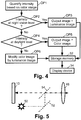
- FIGURE 4 illustrates one suitable algorithm for generating the output image.
- the image intensity is quantified based on the color image. This quanitification can employ an average image intensity, average image intensity per color channel, or other suitable metric.
- the image intensity quantification operation OP1 is performed for sub-regions of the image to enable piecemeal processing of the image.
- the image intensity quantification operation OP1 is optionally replaced by another metric of the color image "quality" such as an image contrast metric.
- the image intensity metric is compared with a intensity night vision level threshold in a comparison operation OP2.
- the objective of this comparison is to determine whether the light intensity is too low for the color image to be useful.
- image “quality” metrics such as image contrast can be used. (In the latter metric, for example, a color image whose image contrast is below a threshold may be assumed to be too dim to be useful). If the comparison operation OP2 indicates that the color image is not useful, then it is assumed that the problem is that the light intensity is too low. In this case, the output image is selected as the acquired luminance image in a selection operation OP3.
- the luminance image has the disadvantage of not being in color (that is, it is a grayscale image)
- the photon counting capability of the set of APD photodetectors APD and associated acquisition circuitry 12 ensures that the luminance image is likely to have useful contrast even in very low light conditions.
- the output image is somewhat analogous to the output of "night vision goggles" or similar devices.
- a second comparison operation OP4 determines whether the color image has intensity corresponding to daylight level. If so, then it is reasonable to assume that the photon counting set of APD photodetectors APD is fully saturated, and accordingly the luminance image is washed out and not useful. In such a case, a second selection operation OP5 selects the color image as the output image.
- a color image modification operation OP6 is performed which adjusts the color image based on corresponding content of the luminance image.
- the modification operation OP6 optionally increases intensity of the red, green, and blue channels of each pixel of the color image by an amount based on the luminance value of the corresponding pixel of the luminance image.
- such intensity enhancement is limited to those regions of the luminance image that have luminance values above a minimum threshold (so that the luminance image is indicating some light is present) and below a maximum threshold (since above such a threshold it may be assumed that the color image successfully captured the higher intensity light).
- a minimum threshold so that the luminance image is indicating some light is present
- a maximum threshold since above such a threshold it may be assumed that the color image successfully captured the higher intensity light.
- Other compositional approaches for modifying the color image based on the luminance image may be used.
- the output image generated by one of the operations OP3, OP5, OP6 is suitably stored in a storage memory 32, displayed on a display device 34, or otherwise utilized.
- the imaging array 10 is a CMOS device
- various components 12, 14, 20, 22, 30, 32, 34 or various combinations of said components may be embodied as separate chips, dies, or so forth, some of which may optionally be fabricated in something other than a silicon-based material system.
- the circuitry components 12, 20, 30 or various portions thereof may be variously embodied as discrete circuitry, integrated circuitry, a suitably programmed microprocessor or microcontroller, or so forth.
- the color imaging device may be a component of, or may be embodied as, substantially any color imaging application device, such as an illustrated digital camera 40 (which may, for example, be a compact digital camera such as are typically used by amateur photographers, or a digital single-lens reflex (SLR) camera such as are typically used by more advanced or professional photographers, or so forth), or a webcam 42 integral with or installed on a computer 44, or so forth.
- the imaging array 10 may view an imaging subject directly, or may be optically coupled with a subject to be imaged by a suitable optical system, such as an illustrated lens 46 of the digital camera 40, or a lens system (not shown) of the webcam 42, or so forth.
- color imaging devices 40, 42 may find application in other application domains such as in medical imaging (for example, as a component of or embodied in an endoscopic device configured for insertion into a subject for internal imaging of the subject under low-light or shadowed conditions), or as a component of or embodied in video equipment for capturing sporting events, and so forth.
- the set of APD photodetectors APD When operated in Geiger mode, the set of APD photodetectors APD extend imaging capability to extremely low light levels, albeit in grayscale. At higher light levels that are still below full daylight illumination, the set of APD photodetectors APD provide a high gain luminance image acquired in Geiger mode or in a less aggressive avalanche multiplication gain mode that can be used to modify or adjust the color image to provide enhanced image contrast or other image enhancement. Because of the high gain provided by the APD photodetectors APD, these substantial advantages can be obtained without replacing a large fraction or percentage of the color-selective photodetectors R, G, B with APD photodetectors APD.
- the APD photodetectors of the set of APD photodetectors make up less than or about one-fourth of the total number of photodetectors of the imaging array.
- the APD photodetectors APD make up precisely one-fourth of the photodetectors of the imaging array.
- FIGURE 5 depicts the color imaging array 10 arranged respective to an optical system 48 to image a subject.
- An optional light source 50 such as a pulsed laser, is coupled into the optical system 48 using a first prism or mirror 52 and a second prism or mirror 54 that is partially reflective and partially transmissive.
- the optional pulsed laser or other light source 50 generates a light pulse that travels through the optical system 48, reflects (at least in part) off of the subject, the (at least partially) reflected light is collected by the optical system 48 and imaged by the imaging array 10.
- the set of APD photodetectors APD operating in Geiger mode are configured with sufficient temporal resolution to detect the delay time between activation of the optional light source 50 and photon counts acquired by the set of APD photodetectors APD responsive to the light pulse generated by activation of the optional light source 50.
- the light source 50 is a pulsed semiconductor laser, pulsed light-emitting diode, or other pulsed narrowband light source, and the APD photodetectors APD are covered by a narrow-band filter tuned to the wavelength of the light source 50 to block ambient light from being detected.
- the prism or mirror 54 is almost completely transmissive for most of the visible spectrum (for example, by being made out of glass or another highly transparent material), but is made partially reflective for the wavelength of the light source 50 by disposing on the prism or mirror 54 dielectric layers defining a narrow-band Bragg reflector tuned to have peak reflectance at the wavelength of the light source 50.
- time-to-digital converters typically employ a substantial number of time-to-digital converters to achieve high depth resolution in the centimeter range. However, if a high depth resolution is not required, then a less complex scheme can be employed.
- the sensor lines are read out sequentially with a well defined time step of typically few nanoseconds. So, the depth difference between two subsequent lines is in the order of few tens of centimeters.
- the time offset between activation of the light source 50 and the start of the APD photodetectors readout the entire depth range is covered by all the lines.
- the scene is illuminated by several millions of short light pulses with slowly increasing time step and frames are collected for every depth of the scene.
- the light pulses can be interleaved with the readouts.
- FIGURE 8 when using the depth estimation scheme of FIGURE 6 or of FIGURE 7 , for each pixel the received photons are suitably collected in depth histograms. Each bin of the histogram contains the number of photons received by the pixel with a time-of-flight less than or equal the depth d .
- FIGURE 8 diagrammatically shows an example of such a histogram for two objects at two different distances. The histogram is plotted using a solid line in FIGURE 8 . The derivative of the histogram is plotted using a dashed line in FIGURE 8 .
- the two peaks in the derivative of the histogram correspond to the depth positions of the two viewed objects (the two viewed objects are either along different lines of sight, or the front object is a transparent object such as a window pane) or two distinct portions of a single viewed object spanning different depth positions. More generally, each peak in the histogram derivative corresponds to the depth of an object.
- the differentiation of the histogram increases the noise. Accordingly, the number of measurements (corresponding to the number of light source activation events and corresponding acquisitions) should be sufficient to provide depth localization of the objects at the desired noise level. Noise reducing signal processing techniques can also be applied.
- the imaging array is a single integrated imaging array in which the APD photodetectors APD are interspersed with the color-selective photodetectors R, G, B.
- This approach facilitates fabrication of a compact color imaging device, and also ensures spatial registration of the acquired color image and the acquired luminance image.
- the integrated approach can make manufacturing more difficult.
- replacing a conventional color imaging array with the integrated imaging array 10 entails modification of both the color imaging array and of coupling electronics of the color image acquisition circuitry.
- an APD photodetectors array APDA is included as an add-on component of an existing color imaging system.
- the existing color imaging system can use a color imaging array with red, green, and blue photodetectors (variation not illustrated), or as illustrated can use a separate red photodetector array RA, green photodetector array GA, and blue photodetector array BA.
- the optical system 48 is again used to capture light from the subject, and partially reflective/partially transmissive prisms or mirrors 60, 62, 64 are used to couple selected fractions of the light from the subject to each of the imaging arrays RA, GA, BA, APDA.
- the color image is acquired by combining the color channel images generated by the respective three color-selective arrays RA, GA, BA, while the luminance image is generated by the APD photodetectors array APDA.
- Remaining components shown in FIGURE 1 such as the digital image processing circuitry 30, can be utilized in the system of FIGURE 9 .
- the optional light source 50 is included for use in acquiring depth information, and is coupled into the optical system 48 via the partially reflective mirror 60 and an additional partially reflective/partially transmissive mirror 66.
- the light source 50 can also be configured to illuminate the subject via an optical pathway that does not include the optical system 48.
- the light source 50 is arranged to directly illuminate the subject without any intervening optics.
Description
- The following relates to the imaging arts, photographic arts, audio/video arts, remote communication arts, and related arts.
- Digital imaging is used in diverse applications such as digital cameras, web cameras ("webcams"), audio/video cameras ("camcorders"), and so forth. In a known approach, a CMOS imager is employed, in which an array of broadband photodetectors are coupled with color-selective filters to define color-selective photodetectors. In consideration of relative light detection sensitivity factors for different colors, such CMOS color imaging arrays sometimes employ a Bayer pattern that includes 50% green photodetectors, 25% blue photodetectors, and 25% red photodetectors. The color-selective photodetectors are biased through a reset transistor, and impingement of light generates a detectable voltage reduction. To provide sensitivity to low light levels, the voltage can be amplified by suitable amplification circuitry.
- A known problem with CMOS imagers is that they have poor sensitivity to low light conditions, even when operated in conjunction with signal amplification circuitry. One source of light intensity loss is the color-selective filters. For a given light intensity, each color-selective filter typically removes about two-thirds of the light (corresponding to the non-selected colors), although the filtering loss is dependent upon the type of filter used.
- One solution to this problem is to intersperse "panchromatic" photodetectors amongst the color-selective photodetectors of the color imaging array. The panchromatic photodetectors are similar to the color-selective photodetectors, but do not have color-selective filters. The panchromatic photodetectors generate a luminance image, which is an image of light intensity substantially independent of light color or wavelength, as acquired by broadband or panchromatic photodetectors. (It will be appreciated that the luminance image may still have some wavelength dependence due to possible non-flat light sensitivity-versus-wavelength dependence of the broadband or panchromatic photodetectors.) Digital image processing circuitry combines the color image generated by the color-selective photodetectors and the luminance image generated by the broadband or panchromatic photodetectors to generate an output image. Some systems employing such interspersed color-selective and panchromatic photodetectors are described, for example, in
U.S. Publ. Appl. No. 2008/0130991 A1 and inU.S. Publ. Appl. No. 2008/0130073 A1 as well as inWO 2008/150021 A1 . - The approach of interspersing color-selective and panchromatic photodetectors in a color imaging array improves light sensitivity due at least to the removal of the color-selective filters in the panchromatic photodetectors. A further advantage is that the electronics are similar for both the color-selective and panchromatic photodetectors, which simplifies imaging array fabrication.
- However, the improvement in light intensity sensitivity using this approach is limited, and is influenced by the tradeoff between color-selective and panchromatic photodetector densities in the imaging array. In some arrays disclosed of
U.S. Publ. Appl. No. 2008/0130991 A1 and inU.S. Publ. Appl. No. 2008/0130073 A1 , about one-half of the array comprises panchromatic photodetectors. An array having a higher number of panchromatic photodetectors than color-selective photodetectors is disclosed inEP 0354382 A1 . This high density of panchromatic photodetectors in the array can be expected to adversely affect color sensitivity and color differentiation capabilities of the array. Moreover, even with the color-selective filters omitted, the light sensitivity of the panchromatic portion of the imaging array is limited due to the noise of the detector itself. -
EP 1973160 A2 discloses an image sensor including an imaging area including a plurality of cells arrayed in a matrix on a semiconductor substrate, each of the cells including an avalanche photodiode. - The following provides new and improved apparatuses and methods which overcome the above-referenced problems and others, as defined in the independent claims.
- One advantage resides in providing color imaging with improved intensity range.
- Another advantage resides in providing color imaging with depth of field information.
- Another advantage resides in providing color imaging with amplification.
- Further advantages will be apparent to those of ordinary skill in the art upon reading and understand the following detailed description.
-
FIGURE 1 diagrammatically shows a color imaging device that includes an imaging array comprising color-selective photodetectors and an interspersed set of avalanche photodiode (APD) photodetectors. -
FIGURE 2 diagrammatically shows an electrical schematic of an illustrative blue photodetector of the color imaging device ofFIGURE 1 , and an electrical schematic of an illustrative APD photodetector of the color imaging device ofFIGURE 1 . -
FIGURE 3 diagrammatically shows a readout sequence for reading out the set of APD photodetectors of the imaging array ofFIGURE 1 . -
FIGURE 4 diagrammatically shows a flow chart of illustrative processing suitably performed by the digital image processing circuitry of the color imaging device ofFIGURE 1 . -
FIGURE 5 diagrammatically shows imaging optics suitably used in the color imaging device ofFIGURE 1 , which in the embodiment ofFIGURE 5 include a light source for acquiring depth information using the set of APD photodetectors. -
FIGURES 6 and 7 diagrammatically show timing diagrams for acquiring depth information using the embodiment ofFIGURE 5 . -
FIGURE 8 diagrammatically plots photon counts as a function of time offset or depth acquired using the depth estimation approach ofFIGURE 6 or ofFIGURE 7 . -
FIGURE 9 diagrammatically shows another embodiment in which the color-selective photodetectors are segregated into mono-color arrays, the set of APD photodetectors is segregated into an APD array, imaging optics couple light to these arrays, and a light source is provided for acquiring depth information using the APD array. - With reference to
FIGURES 1 and2 , acolor imaging array 10 includes an array of color selective photodetectors configured to acquire a color image of a subject. In the illustratedimaging array 10, the color selective photodetectors include: red photodetectors R configured to detect red light; green photodetectors G configured to detect green light; and blue photodetectors B configured to detect blue light. Thecolor imaging array 10 further includes a set of avalanche photodiode (APD) photodetectors APD arranged to acquire a luminance image. An electrical schematic of an illustrative blue photodetector B is depicted inFIGURE 2 . In this illustrative example, the blue photodetector B is a CMOS photodetector including a photodiode D that is pre-charged to a low voltage bias vdd through a reset transistor R1. During the acquisition, electron-hole pairs are photo-generated in the depletion region of the diode D, which lowers the voltage level across the diode D. The diode D can be substantially any type of photodiode, such as a P-I-N photodiode, an avalanche photodiode, or so forth. The voltage is amplified by a source-follower circuit AMP and can be read out through a readout transistor R2. The photodiode D is a broadband photodiode which would in general detect light of substantially any visible wavelength. Accordingly, a color-selective filter F is included to block light other than blue light from reaching the photodetector D. The red and green photodetectors R, G are similar, except that they utilize red-selective and green-selective filters, respectively. -
FIGURE 2 also depicts an electrical schematic of an illustrative APD photodetector APD, which includes an avalanche photodiode DA. An avalanche photodiode is a photodiode that provides internal signal amplification through an avalanche process. The avalanche photodiode DA is reverse-biased at a bias level Vex that is sufficiently high so that photogenerated electrons and holes are accelerated by the internal bias field to generate avalanche multiplication of carriers so as to produce substantial gain. The electrical schematic ofFIGURE 2 configures the avalanche photodiode DA in Geiger mode for photon counting. In other embodiments, a lower bias level can be used to produce avalanche multiplication. In some contemplated embodiments, the same circuit topology as is used for the red, green, and blue photodetectors R, G, B (an illustrative example being depicted in the lefthand side ofFIGURE 2 ) is also used to operate the avalanche photodiode DA, with avalanche multiplication being obtained in the avalanche photodiode DA due to a high internal electric field provided by the p/n junction design of the avalanche photodiode DA. The gain provided by the avalanche photodiode DA means that for every absorbed photon, a cascade of electrons and holes is generated internally within the avalanche photodiode DA. The gain depends upon, among other factors, the bias level Vex. - For a sufficiently high bias level a detectable current pulse is generated responsive to absorption of a single photon, which enables the avalanche photodiode DA to be optionally operated in a Geiger mode to perform photon counting. The electrical schematic of an illustrative APD photodetector APD depicted in
FIGURE 2 is configured for Geiger mode operation. The diode DA is charged to few volts above the breakdown voltage by the bias level Vex, and a readout transistor R3 senses if the avalanche photodiode DA has absorbed a photon. Photons are counted sequentially by reading each photodiode DA at successive intervals. In an array configuration, the READ signal of one line can optionally be used as the RESET signal of the previous line. - The avalanche photodiodes DA of the APD photodetectors APD are typically configured to count any photon in the visible spectrum. Accordingly, the image acquired by the set of APD photodetectors APD is a luminance or grayscale image. However, it is contemplated for the spectral response of the avalanche photodiodes DA to have some wavelength dependence, such as (for example) a sensitivity peak near the middle of the visible spectrum, and/or a sensitivity decrease toward the infrared region and/or toward the ultraviolet region. Illustrated
photon counting circuitry 12 operates the APD photodetectors APD in Geiger mode to generate a luminance image based on photon counts acquired using the APD photodetectors APD. Thephoton counting circuitry 12 receives data output by the set of APD photodetectors APD, and optionally also sends control signals to reset APD photodetectors APD that have been "triggered" by impingement of a photon. Alternatively, the resetting of the APD photodetectors APD may be performed by suitable reset circuitry integrated with each APD photodetector APD. The luminance image acquired by thephoton counting circuitry 12 is stored or buffered in a suitable luminance image memory 14. - In some embodiments, a modification of the APD readout method uses the set of APD photodetectors APD of the
imaging array 10 and varies the excess voltage of each avalanche photodiode DA (that is, varies the bias voltage Vex) to match the photon detection efficiency to the expected photon flux. In these embodiments, the bias voltage Vex is different for different avalanche photodiodes DA of the set of APD photodetectors APD of theimaging array 10. The bias variation can be selected using a lookup table associating bias value for the avalanche photodiode with current in one or more of the neighboring color selective photodetectors R, G, B. This current value is suitably multiplied by the inverse of the photon detection efficiency to account for the reduced photon detection efficiencies at low values of the bias voltage Vex. - With brief reference to
FIGURE 3 , a fast parallel readout scheme can be used to achieve luminance image readout rates of more than 1 million frames per second. As diagrammatically shown inFIGURE 3 , this rapid readout rate can be realized by reading two halves of thearray 10 at the same time and by using more than one data line per column to allow the readout of several lines at the same time. - Although
photon counting circuitry 12 is illustrated, in other embodiments the luminance acquisition circuitry operates the APD photodetectors APD in a non-Geiger mode, for example by biasing the APD photodetectors APD at a lower level so that the APD photodetectors APD provide substantial gain but are not capable of performing individual photon counting as in the Geiger mode. Such a non-Geiger mode still provides intrinsic gain due to avalanche multiplication during breakdown of the junction, so as to provide good sensitivity to low light intensity. - Color
image acquisition circuitry 20 acquires image data from the color-selective photodetectors R, G, B of theimaging array 10, and buffers or stores the resulting color image in acolor image memory 22. The color-selective photodetectors R, G, B and associated colorimage acquisition circuitry 20 suitably operate in accordance with a typical color image device employing a CMOS imaging array. However, because some pixels of the display are occupied by grayscale APD photodetectors APD rather than by color-selective photodetectors R, G, B, some scaling of the various color channels may be appropriate. In the illustratedimaging array 10, for example, densities of the red, green, blue, and APD photodetectors R, G, B, APD in thearray 10 are about 25%, 25%, 25%, and 25%, respectively. That is, about 25% of the photodetectors are red photodetectors R; about 25% of the photodetectors are green photodetectors G; about 25% of the photodetectors are blue photodetectors B; and about 25% of the photodetectors are APD photodetectors APD. Thearray 10 is obtained by starting with a conventional Bayer pattern that includes 50% green photodetectors, 25% blue photodetectors, and 25% red photodetectors, and replacing about one-half of the green photodetectors with APD photodetectors. As a consequence, the green channel intensity of the raw image will be reduced by one-half as compared with the conventional Bayer pattern. The colorimage acquisition circuitry 20 accommodates this reduction in density of green photodetectors G by suitable scaling of the green image channel. - With returning reference to
FIGURE 1 and with further reference toFIGURE 4 , digitalimage processing circuitry 30 is configured to process the acquired color image and the acquired luminance image to generate an output image.FIGURE 4 illustrates one suitable algorithm for generating the output image. In a first operation OP1, the image intensity is quantified based on the color image. This quanitification can employ an average image intensity, average image intensity per color channel, or other suitable metric. In some embodiments, the image intensity quantification operation OP1 is performed for sub-regions of the image to enable piecemeal processing of the image. Moreover, the image intensity quantification operation OP1 is optionally replaced by another metric of the color image "quality" such as an image contrast metric. - The image intensity metric is compared with a intensity night vision level threshold in a comparison operation OP2. The objective of this comparison is to determine whether the light intensity is too low for the color image to be useful. Again, other image "quality" metrics such as image contrast can be used. (In the latter metric, for example, a color image whose image contrast is below a threshold may be assumed to be too dim to be useful). If the comparison operation OP2 indicates that the color image is not useful, then it is assumed that the problem is that the light intensity is too low. In this case, the output image is selected as the acquired luminance image in a selection operation OP3. Although the luminance image has the disadvantage of not being in color (that is, it is a grayscale image), the photon counting capability of the set of APD photodetectors APD and associated
acquisition circuitry 12 ensures that the luminance image is likely to have useful contrast even in very low light conditions. The output image is somewhat analogous to the output of "night vision goggles" or similar devices. - On the other hand, if the comparison operation OP2 indicates that the color image is useful, then a second comparison operation OP4 determines whether the color image has intensity corresponding to daylight level. If so, then it is reasonable to assume that the photon counting set of APD photodetectors APD is fully saturated, and accordingly the luminance image is washed out and not useful. In such a case, a second selection operation OP5 selects the color image as the output image.
- Finally, if both comparison operations OP2, OP4 are negative, then it is determined that the color image is useful but may be improved based on grayscale information provided by the luminance image. In such a case, a color image modification operation OP6 is performed which adjusts the color image based on corresponding content of the luminance image. In a computationally straightforward approach, the modification operation OP6 optionally increases intensity of the red, green, and blue channels of each pixel of the color image by an amount based on the luminance value of the corresponding pixel of the luminance image. In a variant approach, such intensity enhancement is limited to those regions of the luminance image that have luminance values above a minimum threshold (so that the luminance image is indicating some light is present) and below a maximum threshold (since above such a threshold it may be assumed that the color image successfully captured the higher intensity light). Other compositional approaches for modifying the color image based on the luminance image may be used.
- With continuing reference to
FIGURES 1 and4 , the output image generated by one of the operations OP3, OP5, OP6 is suitably stored in astorage memory 32, displayed on adisplay device 34, or otherwise utilized. In embodiments in which theimaging array 10 is a CMOS device, it is contemplated to integratevarious components various components circuitry components - The color imaging device may be a component of, or may be embodied as, substantially any color imaging application device, such as an illustrated digital camera 40 (which may, for example, be a compact digital camera such as are typically used by amateur photographers, or a digital single-lens reflex (SLR) camera such as are typically used by more advanced or professional photographers, or so forth), or a
webcam 42 integral with or installed on acomputer 44, or so forth. Theimaging array 10 may view an imaging subject directly, or may be optically coupled with a subject to be imaged by a suitable optical system, such as an illustratedlens 46 of thedigital camera 40, or a lens system (not shown) of thewebcam 42, or so forth. Moreover, although consumer- or business-relatedapplication devices - Integration of the set of APD photodetectors APD in the
color imaging array 10 has numerous advantages. When operated in Geiger mode, the set of APD photodetectors APD extend imaging capability to extremely low light levels, albeit in grayscale. At higher light levels that are still below full daylight illumination, the set of APD photodetectors APD provide a high gain luminance image acquired in Geiger mode or in a less aggressive avalanche multiplication gain mode that can be used to modify or adjust the color image to provide enhanced image contrast or other image enhancement. Because of the high gain provided by the APD photodetectors APD, these substantial advantages can be obtained without replacing a large fraction or percentage of the color-selective photodetectors R, G, B with APD photodetectors APD. In some embodiments, the APD photodetectors of the set of APD photodetectors make up less than or about one-fourth of the total number of photodetectors of the imaging array. For example, in theillustrative imaging array 10, the APD photodetectors APD make up precisely one-fourth of the photodetectors of the imaging array. - With reference to
FIGURE 5 , in some embodiments the set of APD photodetectors APD are used to acquire depth information.FIGURE 5 depicts thecolor imaging array 10 arranged respective to anoptical system 48 to image a subject. An optionallight source 50, such as a pulsed laser, is coupled into theoptical system 48 using a first prism ormirror 52 and a second prism ormirror 54 that is partially reflective and partially transmissive. The optional pulsed laser or otherlight source 50 generates a light pulse that travels through theoptical system 48, reflects (at least in part) off of the subject, the (at least partially) reflected light is collected by theoptical system 48 and imaged by theimaging array 10. The set of APD photodetectors APD operating in Geiger mode are configured with sufficient temporal resolution to detect the delay time between activation of the optionallight source 50 and photon counts acquired by the set of APD photodetectors APD responsive to the light pulse generated by activation of the optionallight source 50. - In one embodiment providing depth information, the
light source 50 is a pulsed semiconductor laser, pulsed light-emitting diode, or other pulsed narrowband light source, and the APD photodetectors APD are covered by a narrow-band filter tuned to the wavelength of thelight source 50 to block ambient light from being detected. In some such embodiments, the prism ormirror 54 is almost completely transmissive for most of the visible spectrum (for example, by being made out of glass or another highly transparent material), but is made partially reflective for the wavelength of thelight source 50 by disposing on the prism ormirror 54 dielectric layers defining a narrow-band Bragg reflector tuned to have peak reflectance at the wavelength of thelight source 50. - To perform depth estimation, the
photon counting circuitry 12 includes time-to-digital converters that generate a time index corresponding to each photon count. The time index is then compared with the time of activation of thelight source 50 to ascertain the round trip travel time of the light, from which the distance can be determined as d = c · t / 2 where c denotes the speed of light, t denotes the round-trip travel time (that is, the time between activation of thelight source 50 and photon count), and d denotes the depth. - Typically, a substantial number of time-to-digital converters are employed to achieve high depth resolution in the centimeter range. However, if a high depth resolution is not required, then a less complex scheme can be employed.
- With reference to
FIGURE 6 , in this less complex scheme the sensor lines are read out sequentially with a well defined time step of typically few nanoseconds. So, the depth difference between two subsequent lines is in the order of few tens of centimeters. By changing the time offset between activation of thelight source 50 and the start of the APD photodetectors readout, the entire depth range is covered by all the lines. In this approach, the scene is illuminated by several millions of short light pulses with slowly increasing time step and frames are collected for every depth of the scene. - With reference to
FIGURE 7 , in a variant scheme that further speeds up the readout (that is, collects more frames to gain better statistics) the light pulses can be interleaved with the readouts. - With reference to
FIGURE 8 , when using the depth estimation scheme ofFIGURE 6 or ofFIGURE 7 , for each pixel the received photons are suitably collected in depth histograms. Each bin of the histogram contains the number of photons received by the pixel with a time-of-flight less than or equal the depth d.FIGURE 8 diagrammatically shows an example of such a histogram for two objects at two different distances. The histogram is plotted using a solid line inFIGURE 8 . The derivative of the histogram is plotted using a dashed line inFIGURE 8 . The two peaks in the derivative of the histogram (dashed line) correspond to the depth positions of the two viewed objects (the two viewed objects are either along different lines of sight, or the front object is a transparent object such as a window pane) or two distinct portions of a single viewed object spanning different depth positions. More generally, each peak in the histogram derivative corresponds to the depth of an object. The differentiation of the histogram increases the noise. Accordingly, the number of measurements (corresponding to the number of light source activation events and corresponding acquisitions) should be sufficient to provide depth localization of the objects at the desired noise level. Noise reducing signal processing techniques can also be applied. - In the embodiment of
FIGURES 1 and5 , the imaging array is a single integrated imaging array in which the APD photodetectors APD are interspersed with the color-selective photodetectors R, G, B. This approach facilitates fabrication of a compact color imaging device, and also ensures spatial registration of the acquired color image and the acquired luminance image. However, the integrated approach can make manufacturing more difficult. Additionally, replacing a conventional color imaging array with theintegrated imaging array 10 entails modification of both the color imaging array and of coupling electronics of the color image acquisition circuitry. - With reference to
FIGURE 9 , in an alternative approach an APD photodetectors array APDA is included as an add-on component of an existing color imaging system. The existing color imaging system can use a color imaging array with red, green, and blue photodetectors (variation not illustrated), or as illustrated can use a separate red photodetector array RA, green photodetector array GA, and blue photodetector array BA. In the embodiment ofFIGURE 9 , theoptical system 48 is again used to capture light from the subject, and partially reflective/partially transmissive prisms or mirrors 60, 62, 64 are used to couple selected fractions of the light from the subject to each of the imaging arrays RA, GA, BA, APDA. The color image is acquired by combining the color channel images generated by the respective three color-selective arrays RA, GA, BA, while the luminance image is generated by the APD photodetectors array APDA. Remaining components shown inFIGURE 1 , such as the digitalimage processing circuitry 30, can be utilized in the system ofFIGURE 9 . In the illustrative alternative system ofFIGURE 9 , the optionallight source 50 is included for use in acquiring depth information, and is coupled into theoptical system 48 via the partiallyreflective mirror 60 and an additional partially reflective/partiallytransmissive mirror 66. - In either embodiment of
FIGURES 5 and9 , thelight source 50 can also be configured to illuminate the subject via an optical pathway that does not include theoptical system 48. For example, in some contemplated embodiments thelight source 50 is arranged to directly illuminate the subject without any intervening optics. - The invention has been described with reference to the preferred embodiments. Modifications and alterations may occur to others upon reading and understanding the preceding detailed description. It is intended that the invention be construed as including all such modifications and alterations insofar as they come within the scope of the appended claims or the equivalents thereof.
Claims (13)
- A color imaging device comprising:one or more arrays (10, RA, GA, BA) of color-selective photodetectors (R, G, B) configured to acquire a color image of a subject;digital image processing circuitry (30) configured to select the color image and/or a luminance image to generate an output image of the subject,wherein the digital image processing circuitry (30) is configuredto quantify an image intensity metric based on the color image, andto compare the image intensity metric with an intensity night vision level threshold and to select the output image as the luminance image of the subject if the image intensity metric is below the intensity night vision level threshold, characterized bya set of avalanche photodiode photodetectors (APD) arranged to acquire the luminance image of the subject;wherein the digital image processing circuitry (30) is further configuredto compare the image intensity metric with an intensity daylight level threshold and to select the output image as the color image of the subject if the image intensity metric is above the intensity night vision level threshold and above the intensity daylight level threshold,to generate a modified color image by adjusting the color image based on corresponding content of the luminance image and to select the output image as the modified color image of the subject if the image intensity metric is above the intensity night vision level threshold and below the intensity daylight level threshold.
- The color imaging device as set forth in claim 1, wherein the avalanche photodiode photodetectors (APD) are interspersed amongst color-selective photodetectors (R, G, B) of the one or more arrays (10) of color-selective photodetectors.
- The color imaging device as set forth in claim 2, wherein the one or more arrays (10) of color-selective photodetectors comprise a single array of photodetectors having interspersed red, green, and blue photodetectors (R, G, B).
- The color imaging device as set forth in claim 3, wherein avalanche photodiode photodetectors (APD) comprise less than or about one-fourth of the total number of photodetectors (APD, R, G, B) of the array (10) of photodetectors.
- The color imaging device as set forth in claim 1, wherein the set of avalanche photodiode photodetectors (APD) defines an array (APDA) that is separate from the one or more arrays (RA, GA, BA) of color-selective photodetectors (R, G, B).
- The color imaging device as set forth in any one of claims 1-5, further comprising:
photon counting circuitry (12) operating the avalanche photodiode photodetectors (APD) in Geiger mode to generate the luminance image based on photon counts acquired using the avalanche photodiode photodetectors. - The color imaging device as set forth in claim 6, wherein the digital image processing circuitry (30) is configured to adjust at least a portion of the acquired color image based on a corresponding portion of the acquired luminance image.
- The color imaging device as set forth in any one of claims 6-7, wherein the digital image processing circuitry (30) is configured to generate depth information based on delay time between activation of a light source (50) and photon counts acquired using the avalanche photodiode photodetectors (APD).
- The color imaging device as set forth in any one of claims 1-8, wherein the one or more arrays (10, RA, GA, BA) of color selective photodetectors (R, G, B) and the set of avalanche photodiode photodetectors (APD) both comprise CMOS devices.
- The color imaging device as set forth in any one of claims 1-9, further comprising:
imaging optics (48) optically coupling light from the subject to the one or more arrays (10, RA, GA, BA) of color-selective photodetectors (R, G, B) and to the set of avalanche photodiode photodetectors (APD) to enable acquisition of the color image and of the luminance image of the subject. - The color imaging device as set forth in any one of claims 1-10, wherein the color imaging device comprises a digital camera (40) or web camera (42).
- The color imaging device as set forth in any one of claims 1-10, wherein the color imaging device comprises a medical imaging device.
- A color imaging method comprising:imaging a subject using one or more arrays (10, RA, GA, BA) of color-selective photodetectors (R, G, B) configured to acquire a color image of a subject and a set of avalanche photodiode photodetectors (APD) arranged to acquire a luminance image of the subject; andquantifying an image intensity metric based on the color image,comparing the image intensity metric with an intensity night vision level threshold and selecting the output image as the luminance image of the subject if the image intensity metric is below the intensity night vision level threshold,comparing the image intensity metric with an intensity daylight level threshold and selecting the output image as the color image of the subject if the image intensity metric is above the intensity night vision level threshold and above the intensity daylight level threshold,adjusting the color image based on corresponding content of the luminance image to generate a modified color image and selecting the output image as the modified color image of the subject if the image intensity metric is above the intensity night vision level threshold and below the intensity daylight level threshold.
Applications Claiming Priority (2)
| Application Number | Priority Date | Filing Date | Title |
|---|---|---|---|
| US13973908P | 2008-12-22 | 2008-12-22 | |
| PCT/IB2009/055194 WO2010073137A1 (en) | 2008-12-22 | 2009-11-19 | Cmos imager with single photon counting capability |
Publications (2)
| Publication Number | Publication Date |
|---|---|
| EP2380038A1 EP2380038A1 (en) | 2011-10-26 |
| EP2380038B1 true EP2380038B1 (en) | 2019-01-09 |
Family
ID=41667181
Family Applications (1)
| Application Number | Title | Priority Date | Filing Date |
|---|---|---|---|
| EP09774935.2A Active EP2380038B1 (en) | 2008-12-22 | 2009-11-19 | Cmos imager |
Country Status (5)
| Country | Link |
|---|---|
| US (1) | US8610808B2 (en) |
| EP (1) | EP2380038B1 (en) |
| JP (1) | JP2012513694A (en) |
| CN (1) | CN102265176B (en) |
| WO (1) | WO2010073137A1 (en) |
Families Citing this family (40)
| Publication number | Priority date | Publication date | Assignee | Title |
|---|---|---|---|---|
| US8716643B2 (en) * | 2010-09-06 | 2014-05-06 | King Abdulaziz City Science And Technology | Single photon counting image sensor and method |
| US9052497B2 (en) | 2011-03-10 | 2015-06-09 | King Abdulaziz City For Science And Technology | Computing imaging data using intensity correlation interferometry |
| US9099214B2 (en) | 2011-04-19 | 2015-08-04 | King Abdulaziz City For Science And Technology | Controlling microparticles through a light field having controllable intensity and periodicity of maxima thereof |
| ITTO20110689A1 (en) * | 2011-07-28 | 2013-01-29 | St Microelectronics Srl | SPECTROMETER INCLUDING AN AVALANCHE PHOTODIODO OPERATING IN GEIGER MODE |
| EP2740262B1 (en) | 2011-08-03 | 2020-09-09 | Koninklijke Philips N.V. | Position-sensitive readout modes for digital silicon photomultiplier arrays |
| US8471205B2 (en) * | 2011-08-25 | 2013-06-25 | Bae Systems Information And Electronic Systems Integration Inc. | Hybrid photodiode/APD focal plane array for solid state low light level imagers |
| WO2013066959A1 (en) * | 2011-10-31 | 2013-05-10 | The Trustees Of Columbia University In The City Of New York | Systems and methods for imaging using single photon avalanche diodes |
| US8736008B2 (en) | 2012-01-04 | 2014-05-27 | General Electric Company | Photodiode array and methods of fabrication |
| WO2013118065A1 (en) * | 2012-02-06 | 2013-08-15 | Biooptico Ab | Camera arrangement and image processing method for quantifying tissue structure and degeneration |
| WO2013128998A1 (en) * | 2012-02-27 | 2013-09-06 | ソニー株式会社 | Imaging element and electronic equipment |
| CN102662165A (en) * | 2012-05-24 | 2012-09-12 | 中国科学院光电研究院 | Active-passive composite array type photoelectric detection device |
| CA2878514A1 (en) | 2012-07-26 | 2014-01-30 | Olive Medical Corporation | Ycbcr pulsed illumination scheme in a light deficient environment |
| CA2878511A1 (en) | 2012-07-26 | 2014-01-30 | Olive Medical Corporation | Continuous video in a light deficient environment |
| US9036065B1 (en) | 2012-08-16 | 2015-05-19 | Rambus Inc. | Shared-counter image sensor |
| US9679929B2 (en) | 2012-10-12 | 2017-06-13 | Samsung Electronics Co., Ltd. | Binary image sensors including quantum dots and unit pixels thereof |
| US9432604B2 (en) | 2012-10-12 | 2016-08-30 | Samsung Electronics Co., Ltd. | Image sensor chips |
| AU2014223163A1 (en) | 2013-02-28 | 2015-08-20 | Olive Medical Corporation | Videostroboscopy of vocal chords with CMOS sensors |
| EP3459431A1 (en) | 2013-03-15 | 2019-03-27 | DePuy Synthes Products, Inc. | Controlling the integral light energy of a laser pulse |
| WO2014144947A1 (en) | 2013-03-15 | 2014-09-18 | Olive Medical Corporation | Super resolution and color motion artifact correction in a pulsed color imaging system |
| AU2014233464B2 (en) | 2013-03-15 | 2018-11-01 | DePuy Synthes Products, Inc. | Scope sensing in a light controlled environment |
| EP3119265B1 (en) | 2014-03-21 | 2019-09-11 | DePuy Synthes Products, Inc. | Card edge connector for an imaging sensor |
| EP2955544B1 (en) * | 2014-06-11 | 2020-06-17 | Sony Depthsensing Solutions N.V. | A TOF camera system and a method for measuring a distance with the system |
| CN104075802B (en) * | 2014-07-09 | 2016-01-06 | 南京发艾博光电科技有限公司 | A kind of photon counting-type faint optical signal measurement mechanism of high dynamic range and method |
| CN104796674A (en) * | 2015-04-17 | 2015-07-22 | 南京理工大学 | Compressed sensing based color imaging device and compressed sensing based color imaging method |
| WO2017038542A1 (en) * | 2015-09-03 | 2017-03-09 | ソニーセミコンダクタソリューションズ株式会社 | Solid-state image pickup element and electronic device |
| US10381502B2 (en) | 2015-09-09 | 2019-08-13 | Teledyne Scientific & Imaging, Llc | Multicolor imaging device using avalanche photodiode |
| JP2017075906A (en) * | 2015-10-16 | 2017-04-20 | 浜松ホトニクス株式会社 | Distance measurement device |
| EP3388858A4 (en) * | 2015-12-08 | 2018-12-12 | Panasonic Intellectual Property Management Co., Ltd. | Solid-state imaging device, distance measuring device, and distance measurement method |
| WO2019041267A1 (en) * | 2017-08-31 | 2019-03-07 | SZ DJI Technology Co., Ltd. | Systems and methods for an apd array solid-state laser radar |
| JP7019894B2 (en) | 2017-08-31 | 2022-02-16 | エスゼット ディージェイアイ テクノロジー カンパニー リミテッド | How to detect objects and sensor systems |
| JP6862386B2 (en) * | 2018-03-22 | 2021-04-21 | 株式会社東芝 | Photodetector, lidar device, and method of manufacturing photodetector |
| EP3805795A4 (en) * | 2018-05-24 | 2021-08-11 | Sony Semiconductor Solutions Corporation | Time measurement device |
| US11054546B2 (en) | 2018-07-16 | 2021-07-06 | Faro Technologies, Inc. | Laser scanner with enhanced dymanic range imaging |
| JP7114396B2 (en) | 2018-08-03 | 2022-08-08 | キヤノン株式会社 | imaging device, imaging system, moving body |
| US11272112B2 (en) * | 2018-08-08 | 2022-03-08 | Canon Kabushiki Kaisha | Image capturing apparatus |
| JP7293002B2 (en) * | 2018-08-08 | 2023-06-19 | キヤノン株式会社 | Imaging device |
| EP3848965A1 (en) * | 2018-09-06 | 2021-07-14 | Panasonic Intellectual Property Management Co., Ltd. | Solid-state imaging element, imaging system, method for driving solid-state imaging element, and photodetector |
| JP7218193B2 (en) * | 2019-01-31 | 2023-02-06 | キヤノン株式会社 | Imaging device |
| US20230335024A1 (en) * | 2020-09-23 | 2023-10-19 | Sony Interactive Entertainment Inc. | Position information acquisition device, head-mounted display, and position information acquisition method |
| US11624653B2 (en) * | 2020-12-03 | 2023-04-11 | Artilux, Inc. | Multi-application optical sensing apparatus and method thereof |
Citations (2)
| Publication number | Priority date | Publication date | Assignee | Title |
|---|---|---|---|---|
| EP0354382A1 (en) * | 1988-07-20 | 1990-02-14 | Geutebrück Videotechnik Gmbh | Optical surveillance device |
| EP1973160A2 (en) * | 2007-03-22 | 2008-09-24 | Kabushiki Kaisha Toshiba | Image sensor, single-plate color image sensor, and electronic device |
Family Cites Families (55)
| Publication number | Priority date | Publication date | Assignee | Title |
|---|---|---|---|---|
| US4003655A (en) * | 1975-04-17 | 1977-01-18 | The United States Of America As Represented By The Secretary Of The Army | Hybrid silicon avalanche quadrant detector |
| US4366377A (en) * | 1980-09-29 | 1982-12-28 | Mcdonnell Douglas Corporation | Dual sensitivity optical sensor |
| US4616247A (en) * | 1983-11-10 | 1986-10-07 | At&T Bell Laboratories | P-I-N and avalanche photodiodes |
| JPH0799868B2 (en) * | 1984-12-26 | 1995-10-25 | 日本放送協会 | Solid-state imaging device |
| JPH0716256B2 (en) * | 1985-12-18 | 1995-02-22 | ソニー株式会社 | Recording circuit of electronic still camera |
| JPS63131292U (en) * | 1987-02-12 | 1988-08-26 | ||
| US5323233A (en) * | 1990-07-31 | 1994-06-21 | Canon Kabushiki Kaisha | Image signal processing apparatus having a color filter with offset luminance filter elements |
| GB2345217A (en) * | 1998-12-23 | 2000-06-28 | Nokia Mobile Phones Ltd | Colour video image sensor |
| US6555890B2 (en) * | 2000-05-23 | 2003-04-29 | Sensors Unlimited, Inc. | Method for combined fabrication of indium gallium arsenide/indium phosphide avalanche photodiodes and p-i-n photodiodes |
| EP1287360A2 (en) * | 2000-06-02 | 2003-03-05 | Zeptosens AG | Kit and method for determining a plurality of analytes |
| JP3949360B2 (en) * | 2000-08-29 | 2007-07-25 | 日本放送協会 | Color image sensor |
| US6774578B2 (en) * | 2000-09-19 | 2004-08-10 | Semiconductor Energy Laboratory Co., Ltd. | Self light emitting device and method of driving thereof |
| US20030048493A1 (en) * | 2001-09-10 | 2003-03-13 | Pontifex Brian Decoursey | Two sensor quantitative low-light color camera |
| US6841816B2 (en) * | 2002-03-20 | 2005-01-11 | Foveon, Inc. | Vertical color filter sensor group with non-sensor filter and method for fabricating such a sensor group |
| US20040178463A1 (en) * | 2002-03-20 | 2004-09-16 | Foveon, Inc. | Vertical color filter sensor group with carrier-collection elements of different size and method for fabricating such a sensor group |
| US6658329B1 (en) | 2002-05-02 | 2003-12-02 | The United States Of America As Represented By The United States National Aeronautics And Space Administration | Video guidance sensor system with laser rangefinder |
| JP4135486B2 (en) * | 2002-12-06 | 2008-08-20 | 日本ビクター株式会社 | Image sensor |
| JP4465958B2 (en) * | 2002-12-18 | 2010-05-26 | 株式会社ニコン | Color imaging device |
| US6914314B2 (en) * | 2003-01-31 | 2005-07-05 | Foveon, Inc. | Vertical color filter sensor group including semiconductor other than crystalline silicon and method for fabricating same |
| US6894265B2 (en) * | 2003-01-31 | 2005-05-17 | Foveon, Inc. | Vertical color filter sensor group and semiconductor integrated circuit fabrication method for fabricating same |
| JP2005006856A (en) * | 2003-06-18 | 2005-01-13 | Olympus Corp | Endoscope apparatus |
| US20060226374A1 (en) * | 2003-08-06 | 2006-10-12 | Gnothis Holding S.A. | Method and device for identifying luminescent molecules according to the fluorescence correlation spectroscopy method |
| JP2005093610A (en) * | 2003-09-16 | 2005-04-07 | Sumitomo Electric Ind Ltd | Optical receiver |
| JP2005183538A (en) * | 2003-12-17 | 2005-07-07 | Sumitomo Electric Ind Ltd | Light receiving element and optical receiver |
| US7515082B2 (en) * | 2003-12-19 | 2009-04-07 | Searete, Llc | Photo-detector filter having a cascaded low noise amplifier |
| US7683308B2 (en) * | 2004-01-12 | 2010-03-23 | Ecole Polytechnique Federale de Lausanne EFPL | Controlling spectral response of photodetector for an image sensor |
| EP1594321A3 (en) * | 2004-05-07 | 2006-01-25 | Dialog Semiconductor GmbH | Extended dynamic range in color imagers |
| US7960702B2 (en) * | 2004-05-20 | 2011-06-14 | Board of Regents of the Nevada System fo Higher Education, on behalf of the University of Nevada, Reno | Photon event distribution sampling apparatus and method |
| US7880785B2 (en) | 2004-07-21 | 2011-02-01 | Aptina Imaging Corporation | Rod and cone response sensor |
| US8183516B2 (en) * | 2004-07-28 | 2012-05-22 | Quantum Semiconductor Llc | Layouts for the monolithic integration of CMOS and deposited photonic active layers |
| US7477304B2 (en) * | 2004-08-26 | 2009-01-13 | Micron Technology, Inc. | Two narrow band and one wide band color filter for increasing color image sensor sensitivity |
| US7653427B2 (en) * | 2004-11-12 | 2010-01-26 | Intra-Medical Imaging LLC | Method and instrument for minimally invasive sentinel lymph node location and biopsy |
| EP1679907A1 (en) * | 2005-01-05 | 2006-07-12 | Dialog Semiconductor GmbH | Hexagonal color pixel structure with white pixels |
| US7547872B2 (en) * | 2005-02-14 | 2009-06-16 | Ecole Polytechnique Federale De Lausanne | Integrated circuit comprising an array of single photon avalanche diodes |
| US7262402B2 (en) * | 2005-02-14 | 2007-08-28 | Ecole Polytechnique Federal De Lausanne | Integrated imager circuit comprising a monolithic array of single photon avalanche diodes |
| EP1865315B1 (en) * | 2005-03-29 | 2019-03-13 | Olympus Corporation | Cell image analyzing method, cell image analyzing device |
| WO2006127967A2 (en) * | 2005-05-25 | 2006-11-30 | Massachusetts Institute Of Technology | Multifocal scanning microscopy systems and methods |
| US20060268357A1 (en) * | 2005-05-25 | 2006-11-30 | Vook Dietrich W | System and method for processing images using centralized image correction data |
| US20070012948A1 (en) * | 2005-07-15 | 2007-01-18 | Dries J C | Combined APD / PIN InGaAs photodetector with microlens structure and method of manufacture |
| US7745816B2 (en) * | 2005-09-27 | 2010-06-29 | Northwestern University | Single-photon detector with a quantum dot and a nano-injector |
| EP1982356B1 (en) * | 2006-02-01 | 2017-03-15 | Koninklijke Philips N.V. | Geiger mode avalanche photodiode |
| JP4846409B2 (en) * | 2006-03-30 | 2011-12-28 | 富士フイルム株式会社 | Solid-state imaging device |
| JP5106870B2 (en) * | 2006-06-14 | 2012-12-26 | 株式会社東芝 | Solid-state image sensor |
| EP2044420A2 (en) * | 2006-07-17 | 2009-04-08 | Max Wiki | Analytical system comprising an arrangement for temporally variable spatial light modulation and detection method implemented thereby |
| US8187541B2 (en) | 2006-09-18 | 2012-05-29 | California Institute Of Technology | Apparatus for detecting target molecules and related methods |
| US7769229B2 (en) | 2006-11-30 | 2010-08-03 | Eastman Kodak Company | Processing images having color and panchromatic pixels |
| US7893976B2 (en) | 2006-12-01 | 2011-02-22 | Eastman Kodak Company | Light sensitivity in image sensors |
| JP2008193163A (en) * | 2007-01-31 | 2008-08-21 | Sanyo Electric Co Ltd | Solid-state imaging apparatus |
| JP4930109B2 (en) * | 2007-03-06 | 2012-05-16 | ソニー株式会社 | Solid-state imaging device, imaging device |
| TWI334732B (en) * | 2007-03-16 | 2010-12-11 | Coretronic Corp | Projector and method for adjusting projective luminance thereof |
| US20080240543A1 (en) * | 2007-03-30 | 2008-10-02 | Wolfgang Ernst Gustav Budach | Calibration and normalization method for biosensors |
| JP2008306379A (en) | 2007-06-06 | 2008-12-18 | Toshiba Corp | Solid-state imaging element |
| US20090060381A1 (en) * | 2007-08-31 | 2009-03-05 | Ethicon Endo-Surgery, Inc. | Dynamic range and amplitude control for imaging |
| US8227884B2 (en) * | 2009-11-04 | 2012-07-24 | Omnivision Technologies, Inc. | Photodetector array having array of discrete electron repulsive elements |
| US20110101201A1 (en) * | 2009-11-04 | 2011-05-05 | Vincent Venezia | Photodetector Array Having Electron Lens |
-
2009
- 2009-11-19 US US13/139,626 patent/US8610808B2/en active Active
- 2009-11-19 WO PCT/IB2009/055194 patent/WO2010073137A1/en active Application Filing
- 2009-11-19 CN CN200980152142.7A patent/CN102265176B/en active Active
- 2009-11-19 EP EP09774935.2A patent/EP2380038B1/en active Active
- 2009-11-19 JP JP2011541648A patent/JP2012513694A/en active Pending
Patent Citations (2)
| Publication number | Priority date | Publication date | Assignee | Title |
|---|---|---|---|---|
| EP0354382A1 (en) * | 1988-07-20 | 1990-02-14 | Geutebrück Videotechnik Gmbh | Optical surveillance device |
| EP1973160A2 (en) * | 2007-03-22 | 2008-09-24 | Kabushiki Kaisha Toshiba | Image sensor, single-plate color image sensor, and electronic device |
Also Published As
| Publication number | Publication date |
|---|---|
| EP2380038A1 (en) | 2011-10-26 |
| US8610808B2 (en) | 2013-12-17 |
| JP2012513694A (en) | 2012-06-14 |
| CN102265176B (en) | 2015-09-30 |
| WO2010073137A1 (en) | 2010-07-01 |
| CN102265176A (en) | 2011-11-30 |
| US20110249148A1 (en) | 2011-10-13 |
Similar Documents
| Publication | Publication Date | Title |
|---|---|---|
| EP2380038B1 (en) | Cmos imager | |
| US7119842B2 (en) | Image capturing device including a spectrally-selectively transmissive diaphragm | |
| CN102970480B (en) | Image capturing device and control method thereof | |
| KR102165399B1 (en) | Gated Sensor Based Imaging System With Minimized Delay Time Between Sensor Exposures | |
| CN102292974B (en) | Image capturing apparatus | |
| JP6243402B2 (en) | Multiple gated pixels per readout | |
| US20100171875A1 (en) | Imager capturing an image with a rolling shutter | |
| KR20200096828A (en) | Systems and methods for determining distance to objects | |
| US20070139548A1 (en) | Image capturing apparatus, image capturing method, and computer-readable medium storing program | |
| JP2002315022A (en) | Three-dimensional image detector | |
| JP2001148808A (en) | Solid-state image pickup device and solid-state image pickup element | |
| JP2004309701A (en) | Range-finding/photometric sensor and camera | |
| US11936987B2 (en) | Image capturing apparatus | |
| JP2006343456A (en) | Focus detecting device, and imaging apparatus | |
| RU59923U1 (en) | CCD CAMERA | |
| US8681263B2 (en) | Imager capturing an image with a rolling shutter using flicker detection | |
| US20190246053A1 (en) | Motion tracking using multiple exposures | |
| JP7293002B2 (en) | Imaging device | |
| EP2471256B1 (en) | Digital camera system and method | |
| US8520128B2 (en) | Auto focus module capable of in-pixel monitoring of amount of received light photographing apparatus using the same | |
| EP3335417B1 (en) | Digital read-out integrated circuit with modulated light source rejection | |
| TWI795903B (en) | Photonics systems and methods | |
| CN115942135A (en) | Device and method for improving dynamic range of CMOS (complementary Metal oxide semiconductor) and photon statistical method | |
| JP2008066352A (en) | Semiconductor device |
Legal Events
| Date | Code | Title | Description |
|---|---|---|---|
| PUAI | Public reference made under article 153(3) epc to a published international application that has entered the european phase |
Free format text: ORIGINAL CODE: 0009012 |
|
| 17P | Request for examination filed |
Effective date: 20110722 |
|
| AK | Designated contracting states |
Kind code of ref document: A1 Designated state(s): AT BE BG CH CY CZ DE DK EE ES FI FR GB GR HR HU IE IS IT LI LT LU LV MC MK MT NL NO PL PT RO SE SI SK SM TR |
|
| DAX | Request for extension of the european patent (deleted) | ||
| RAP1 | Party data changed (applicant data changed or rights of an application transferred) |
Owner name: KONINKLIJKE PHILIPS N.V. Owner name: PHILIPS INTELLECTUAL PROPERTY & STANDARDS GMBH |
|
| 17Q | First examination report despatched |
Effective date: 20150717 |
|
| STAA | Information on the status of an ep patent application or granted ep patent |
Free format text: STATUS: EXAMINATION IS IN PROGRESS |
|
| REG | Reference to a national code |
Ref country code: DE Ref legal event code: R079 Ref document number: 602009056649 Country of ref document: DE Free format text: PREVIOUS MAIN CLASS: G01S0011000000 Ipc: H04N0005369000 |
|
| GRAP | Despatch of communication of intention to grant a patent |
Free format text: ORIGINAL CODE: EPIDOSNIGR1 |
|
| STAA | Information on the status of an ep patent application or granted ep patent |
Free format text: STATUS: GRANT OF PATENT IS INTENDED |
|
| RIC1 | Information provided on ipc code assigned before grant |
Ipc: H04N 5/369 20110101AFI20180711BHEP Ipc: H04N 9/04 20060101ALI20180711BHEP |
|
| INTG | Intention to grant announced |
Effective date: 20180723 |
|
| GRAS | Grant fee paid |
Free format text: ORIGINAL CODE: EPIDOSNIGR3 |
|
| GRAA | (expected) grant |
Free format text: ORIGINAL CODE: 0009210 |
|
| STAA | Information on the status of an ep patent application or granted ep patent |
Free format text: STATUS: THE PATENT HAS BEEN GRANTED |
|
| AK | Designated contracting states |
Kind code of ref document: B1 Designated state(s): AT BE BG CH CY CZ DE DK EE ES FI FR GB GR HR HU IE IS IT LI LT LU LV MC MK MT NL NO PL PT RO SE SI SK SM TR |
|
| REG | Reference to a national code |
Ref country code: GB Ref legal event code: FG4D |
|
| REG | Reference to a national code |
Ref country code: CH Ref legal event code: EP Ref country code: AT Ref legal event code: REF Ref document number: 1088773 Country of ref document: AT Kind code of ref document: T Effective date: 20190115 |
|
| REG | Reference to a national code |
Ref country code: DE Ref legal event code: R096 Ref document number: 602009056649 Country of ref document: DE |
|
| REG | Reference to a national code |
Ref country code: IE Ref legal event code: FG4D |
|
| REG | Reference to a national code |
Ref country code: NL Ref legal event code: MP Effective date: 20190109 |
|
| REG | Reference to a national code |
Ref country code: LT Ref legal event code: MG4D |
|
| PG25 | Lapsed in a contracting state [announced via postgrant information from national office to epo] |
Ref country code: NL Free format text: LAPSE BECAUSE OF FAILURE TO SUBMIT A TRANSLATION OF THE DESCRIPTION OR TO PAY THE FEE WITHIN THE PRESCRIBED TIME-LIMIT Effective date: 20190109 |
|
| REG | Reference to a national code |
Ref country code: AT Ref legal event code: MK05 Ref document number: 1088773 Country of ref document: AT Kind code of ref document: T Effective date: 20190109 |
|
| PG25 | Lapsed in a contracting state [announced via postgrant information from national office to epo] |
Ref country code: FI Free format text: LAPSE BECAUSE OF FAILURE TO SUBMIT A TRANSLATION OF THE DESCRIPTION OR TO PAY THE FEE WITHIN THE PRESCRIBED TIME-LIMIT Effective date: 20190109 Ref country code: NO Free format text: LAPSE BECAUSE OF FAILURE TO SUBMIT A TRANSLATION OF THE DESCRIPTION OR TO PAY THE FEE WITHIN THE PRESCRIBED TIME-LIMIT Effective date: 20190409 Ref country code: ES Free format text: LAPSE BECAUSE OF FAILURE TO SUBMIT A TRANSLATION OF THE DESCRIPTION OR TO PAY THE FEE WITHIN THE PRESCRIBED TIME-LIMIT Effective date: 20190109 Ref country code: SE Free format text: LAPSE BECAUSE OF FAILURE TO SUBMIT A TRANSLATION OF THE DESCRIPTION OR TO PAY THE FEE WITHIN THE PRESCRIBED TIME-LIMIT Effective date: 20190109 Ref country code: PT Free format text: LAPSE BECAUSE OF FAILURE TO SUBMIT A TRANSLATION OF THE DESCRIPTION OR TO PAY THE FEE WITHIN THE PRESCRIBED TIME-LIMIT Effective date: 20190509 Ref country code: PL Free format text: LAPSE BECAUSE OF FAILURE TO SUBMIT A TRANSLATION OF THE DESCRIPTION OR TO PAY THE FEE WITHIN THE PRESCRIBED TIME-LIMIT Effective date: 20190109 Ref country code: LT Free format text: LAPSE BECAUSE OF FAILURE TO SUBMIT A TRANSLATION OF THE DESCRIPTION OR TO PAY THE FEE WITHIN THE PRESCRIBED TIME-LIMIT Effective date: 20190109 |
|
| PG25 | Lapsed in a contracting state [announced via postgrant information from national office to epo] |
Ref country code: LV Free format text: LAPSE BECAUSE OF FAILURE TO SUBMIT A TRANSLATION OF THE DESCRIPTION OR TO PAY THE FEE WITHIN THE PRESCRIBED TIME-LIMIT Effective date: 20190109 Ref country code: HR Free format text: LAPSE BECAUSE OF FAILURE TO SUBMIT A TRANSLATION OF THE DESCRIPTION OR TO PAY THE FEE WITHIN THE PRESCRIBED TIME-LIMIT Effective date: 20190109 Ref country code: BG Free format text: LAPSE BECAUSE OF FAILURE TO SUBMIT A TRANSLATION OF THE DESCRIPTION OR TO PAY THE FEE WITHIN THE PRESCRIBED TIME-LIMIT Effective date: 20190409 Ref country code: IS Free format text: LAPSE BECAUSE OF FAILURE TO SUBMIT A TRANSLATION OF THE DESCRIPTION OR TO PAY THE FEE WITHIN THE PRESCRIBED TIME-LIMIT Effective date: 20190509 Ref country code: GR Free format text: LAPSE BECAUSE OF FAILURE TO SUBMIT A TRANSLATION OF THE DESCRIPTION OR TO PAY THE FEE WITHIN THE PRESCRIBED TIME-LIMIT Effective date: 20190410 |
|
| REG | Reference to a national code |
Ref country code: DE Ref legal event code: R097 Ref document number: 602009056649 Country of ref document: DE |
|
| PG25 | Lapsed in a contracting state [announced via postgrant information from national office to epo] |
Ref country code: AT Free format text: LAPSE BECAUSE OF FAILURE TO SUBMIT A TRANSLATION OF THE DESCRIPTION OR TO PAY THE FEE WITHIN THE PRESCRIBED TIME-LIMIT Effective date: 20190109 Ref country code: DK Free format text: LAPSE BECAUSE OF FAILURE TO SUBMIT A TRANSLATION OF THE DESCRIPTION OR TO PAY THE FEE WITHIN THE PRESCRIBED TIME-LIMIT Effective date: 20190109 Ref country code: EE Free format text: LAPSE BECAUSE OF FAILURE TO SUBMIT A TRANSLATION OF THE DESCRIPTION OR TO PAY THE FEE WITHIN THE PRESCRIBED TIME-LIMIT Effective date: 20190109 Ref country code: RO Free format text: LAPSE BECAUSE OF FAILURE TO SUBMIT A TRANSLATION OF THE DESCRIPTION OR TO PAY THE FEE WITHIN THE PRESCRIBED TIME-LIMIT Effective date: 20190109 Ref country code: IT Free format text: LAPSE BECAUSE OF FAILURE TO SUBMIT A TRANSLATION OF THE DESCRIPTION OR TO PAY THE FEE WITHIN THE PRESCRIBED TIME-LIMIT Effective date: 20190109 Ref country code: CZ Free format text: LAPSE BECAUSE OF FAILURE TO SUBMIT A TRANSLATION OF THE DESCRIPTION OR TO PAY THE FEE WITHIN THE PRESCRIBED TIME-LIMIT Effective date: 20190109 Ref country code: SK Free format text: LAPSE BECAUSE OF FAILURE TO SUBMIT A TRANSLATION OF THE DESCRIPTION OR TO PAY THE FEE WITHIN THE PRESCRIBED TIME-LIMIT Effective date: 20190109 |
|
| PLBE | No opposition filed within time limit |
Free format text: ORIGINAL CODE: 0009261 |
|
| STAA | Information on the status of an ep patent application or granted ep patent |
Free format text: STATUS: NO OPPOSITION FILED WITHIN TIME LIMIT |
|
| PG25 | Lapsed in a contracting state [announced via postgrant information from national office to epo] |
Ref country code: SM Free format text: LAPSE BECAUSE OF FAILURE TO SUBMIT A TRANSLATION OF THE DESCRIPTION OR TO PAY THE FEE WITHIN THE PRESCRIBED TIME-LIMIT Effective date: 20190109 |
|
| 26N | No opposition filed |
Effective date: 20191010 |
|
| PG25 | Lapsed in a contracting state [announced via postgrant information from national office to epo] |
Ref country code: SI Free format text: LAPSE BECAUSE OF FAILURE TO SUBMIT A TRANSLATION OF THE DESCRIPTION OR TO PAY THE FEE WITHIN THE PRESCRIBED TIME-LIMIT Effective date: 20190109 |
|
| PG25 | Lapsed in a contracting state [announced via postgrant information from national office to epo] |
Ref country code: TR Free format text: LAPSE BECAUSE OF FAILURE TO SUBMIT A TRANSLATION OF THE DESCRIPTION OR TO PAY THE FEE WITHIN THE PRESCRIBED TIME-LIMIT Effective date: 20190109 |
|
| REG | Reference to a national code |
Ref country code: CH Ref legal event code: PL |
|
| PG25 | Lapsed in a contracting state [announced via postgrant information from national office to epo] |
Ref country code: LU Free format text: LAPSE BECAUSE OF NON-PAYMENT OF DUE FEES Effective date: 20191119 Ref country code: MC Free format text: LAPSE BECAUSE OF FAILURE TO SUBMIT A TRANSLATION OF THE DESCRIPTION OR TO PAY THE FEE WITHIN THE PRESCRIBED TIME-LIMIT Effective date: 20190109 Ref country code: LI Free format text: LAPSE BECAUSE OF NON-PAYMENT OF DUE FEES Effective date: 20191130 Ref country code: CH Free format text: LAPSE BECAUSE OF NON-PAYMENT OF DUE FEES Effective date: 20191130 |
|
| REG | Reference to a national code |
Ref country code: BE Ref legal event code: MM Effective date: 20191130 |
|
| PG25 | Lapsed in a contracting state [announced via postgrant information from national office to epo] |
Ref country code: IE Free format text: LAPSE BECAUSE OF NON-PAYMENT OF DUE FEES Effective date: 20191119 |
|
| PG25 | Lapsed in a contracting state [announced via postgrant information from national office to epo] |
Ref country code: BE Free format text: LAPSE BECAUSE OF NON-PAYMENT OF DUE FEES Effective date: 20191130 |
|
| REG | Reference to a national code |
Ref country code: DE Ref legal event code: R081 Ref document number: 602009056649 Country of ref document: DE Owner name: PHILIPS GMBH, DE Free format text: FORMER OWNER: PHILIPS INTELLECTUAL PROPERTY & STANDARDS, 20099 HAMBURG, DE |
|
| PG25 | Lapsed in a contracting state [announced via postgrant information from national office to epo] |
Ref country code: CY Free format text: LAPSE BECAUSE OF FAILURE TO SUBMIT A TRANSLATION OF THE DESCRIPTION OR TO PAY THE FEE WITHIN THE PRESCRIBED TIME-LIMIT Effective date: 20190109 |
|
| PG25 | Lapsed in a contracting state [announced via postgrant information from national office to epo] |
Ref country code: HU Free format text: LAPSE BECAUSE OF FAILURE TO SUBMIT A TRANSLATION OF THE DESCRIPTION OR TO PAY THE FEE WITHIN THE PRESCRIBED TIME-LIMIT; INVALID AB INITIO Effective date: 20091119 Ref country code: MT Free format text: LAPSE BECAUSE OF FAILURE TO SUBMIT A TRANSLATION OF THE DESCRIPTION OR TO PAY THE FEE WITHIN THE PRESCRIBED TIME-LIMIT Effective date: 20190109 |
|
| PG25 | Lapsed in a contracting state [announced via postgrant information from national office to epo] |
Ref country code: MK Free format text: LAPSE BECAUSE OF FAILURE TO SUBMIT A TRANSLATION OF THE DESCRIPTION OR TO PAY THE FEE WITHIN THE PRESCRIBED TIME-LIMIT Effective date: 20190109 |
|
| REG | Reference to a national code |
Ref country code: DE Ref legal event code: R079 Ref document number: 602009056649 Country of ref document: DE Free format text: PREVIOUS MAIN CLASS: H04N0005369000 Ipc: H04N0025700000 |
|
| PGFP | Annual fee paid to national office [announced via postgrant information from national office to epo] |
Ref country code: GB Payment date: 20221122 Year of fee payment: 14 Ref country code: FR Payment date: 20221122 Year of fee payment: 14 Ref country code: DE Payment date: 20220628 Year of fee payment: 14 |