EP2378574A1 - Nitride semiconductor light-emitting element, and method for manufacturing same - Google Patents
Nitride semiconductor light-emitting element, and method for manufacturing same Download PDFInfo
- Publication number
- EP2378574A1 EP2378574A1 EP09837457A EP09837457A EP2378574A1 EP 2378574 A1 EP2378574 A1 EP 2378574A1 EP 09837457 A EP09837457 A EP 09837457A EP 09837457 A EP09837457 A EP 09837457A EP 2378574 A1 EP2378574 A1 EP 2378574A1
- Authority
- EP
- European Patent Office
- Prior art keywords
- layer
- contact layer
- light
- nitride semiconductor
- emitting device
- Prior art date
- Legal status (The legal status is an assumption and is not a legal conclusion. Google has not performed a legal analysis and makes no representation as to the accuracy of the status listed.)
- Granted
Links
Images

Classifications
-
- H—ELECTRICITY
- H10—SEMICONDUCTOR DEVICES; ELECTRIC SOLID-STATE DEVICES NOT OTHERWISE PROVIDED FOR
- H10H—INORGANIC LIGHT-EMITTING SEMICONDUCTOR DEVICES HAVING POTENTIAL BARRIERS
- H10H20/00—Individual inorganic light-emitting semiconductor devices having potential barriers, e.g. light-emitting diodes [LED]
- H10H20/80—Constructional details
- H10H20/81—Bodies
- H10H20/822—Materials of the light-emitting regions
- H10H20/824—Materials of the light-emitting regions comprising only Group III-V materials, e.g. GaP
- H10H20/825—Materials of the light-emitting regions comprising only Group III-V materials, e.g. GaP containing nitrogen, e.g. GaN
-
- H—ELECTRICITY
- H10—SEMICONDUCTOR DEVICES; ELECTRIC SOLID-STATE DEVICES NOT OTHERWISE PROVIDED FOR
- H10H—INORGANIC LIGHT-EMITTING SEMICONDUCTOR DEVICES HAVING POTENTIAL BARRIERS
- H10H20/00—Individual inorganic light-emitting semiconductor devices having potential barriers, e.g. light-emitting diodes [LED]
- H10H20/80—Constructional details
- H10H20/81—Bodies
-
- H—ELECTRICITY
- H10—SEMICONDUCTOR DEVICES; ELECTRIC SOLID-STATE DEVICES NOT OTHERWISE PROVIDED FOR
- H10H—INORGANIC LIGHT-EMITTING SEMICONDUCTOR DEVICES HAVING POTENTIAL BARRIERS
- H10H20/00—Individual inorganic light-emitting semiconductor devices having potential barriers, e.g. light-emitting diodes [LED]
- H10H20/01—Manufacture or treatment
- H10H20/011—Manufacture or treatment of bodies, e.g. forming semiconductor layers
- H10H20/013—Manufacture or treatment of bodies, e.g. forming semiconductor layers having light-emitting regions comprising only Group III-V materials
- H10H20/0133—Manufacture or treatment of bodies, e.g. forming semiconductor layers having light-emitting regions comprising only Group III-V materials with a substrate not being Group III-V materials
- H10H20/01335—Manufacture or treatment of bodies, e.g. forming semiconductor layers having light-emitting regions comprising only Group III-V materials with a substrate not being Group III-V materials the light-emitting regions comprising nitride materials
-
- H—ELECTRICITY
- H10—SEMICONDUCTOR DEVICES; ELECTRIC SOLID-STATE DEVICES NOT OTHERWISE PROVIDED FOR
- H10H—INORGANIC LIGHT-EMITTING SEMICONDUCTOR DEVICES HAVING POTENTIAL BARRIERS
- H10H20/00—Individual inorganic light-emitting semiconductor devices having potential barriers, e.g. light-emitting diodes [LED]
- H10H20/80—Constructional details
- H10H20/81—Bodies
- H10H20/816—Bodies having carrier transport control structures, e.g. highly-doped semiconductor layers or current-blocking structures
-
- H—ELECTRICITY
- H10—SEMICONDUCTOR DEVICES; ELECTRIC SOLID-STATE DEVICES NOT OTHERWISE PROVIDED FOR
- H10H—INORGANIC LIGHT-EMITTING SEMICONDUCTOR DEVICES HAVING POTENTIAL BARRIERS
- H10H20/00—Individual inorganic light-emitting semiconductor devices having potential barriers, e.g. light-emitting diodes [LED]
- H10H20/80—Constructional details
- H10H20/83—Electrodes
- H10H20/832—Electrodes characterised by their material
Definitions
- the present invention relates to a nitride semiconductor light-emitting device and a method of manufacturing the same.
- a junction barrier is generally formed when a semiconductor is brought into contact with a metal.
- relatively high contact resistance arises between a semiconductor and an electrode made of a metal material.
- a so-called double heterostructure as a basic structure of a light-emitting device, in which both sides of a layer having a relatively narrow band gap (which layer is referred to as a light-emitting layer) is sandwiched between a p-type semiconductor layer and an n-type semiconductor layer each having a wide band gap (which layers are referred to as cladding layers), power loss is caused due to contact resistance arising between a laminate of semiconductor layers and a pair of electrodes mounted thereto when a voltage is applied between the pair of electrodes.
- JP 2002-141552 and JP 2004-335559 disclose techniques of forming GaN layer and/or an AlGaN layer having Al composition ratio not higher than 30% as a contact layer.
- a contact layer having relatively low Al content in composition thereof as described above causes a problem in that, when it is used for an UV light-emitting device having an emission wavelength of 300 nm or less, UV light generated in a light-emitting layer is absorbed by the contact layer and the external quantum efficiency is decreased, although the contact layer exhibits relatively low contact resistance with respect to an electrode.
- JP 2006-295132 discloses a technique of suppressing reduction in external quantum efficiency by providing between a first light-emitting layer and a GaN contact layer a second light-emitting layer for absorbing UV light generated by the first light-emitting layer and emitting light having a longer wavelength than the absorbed light.
- a problem in this technique in that a relatively large number of layers has to be formed, thereby increasing the production cost.
- An object of the present invention is to provide a nitride semiconductor light-emitting device in which contact resistance generated between an n-contact layer and an n-side electrode is effectively reduced while maintaining satisfactory external quantum efficiency, and also provide a method for of efficiently producing the nitride semiconductor light-emitting device.
- a nitride semiconductor light-emitting device having a semiconductor laminated body including an n-type laminate, a light-emitting layer and a p-type laminate, and an n-side electrode and a p-side electrode, characterized in that: the n-type laminate includes an n-contact layer made of an Al x Ga 1-x N material (0.7 ⁇ x ⁇ 1.0) and an n-clad layer provided on the n-contact layer; and an interlayer made of an Al y Ga 1-y N material (0 ⁇ y ⁇ 0.5) is provided on a partially exposed portion, on the light-emitting layer side, of the n-contact layer.
- a method of producing a nitride semiconductor light-emitting device comprising the steps of: forming a semiconductor laminated body by sequentially growing on a substrate an n-type laminate including an n-contact layer and an n-clad layer, a light-emitting layer, and a p-type laminate including a p-clad layer and a p-contact layer in this order; forming an interlayer and an n-side electrode on the n-contact layer; and forming a p-side electrode on the p-contact layer, wherein the n-contact layer is formed of an Al x Ga 1-x N material (0.7 ⁇ x ⁇ 1.0), and the interlayer is formed of an Al y Ga 1-y N material (0 ⁇ y ⁇ 0.5).
- the nitride semiconductor light-emitting device in which an interlayer made of an Al y Ga 1-y N material (0 ⁇ y ⁇ 0.5) is provided between an n-contact layer made of an Al x Ga 1-x N material (0.7 ⁇ x ⁇ 1.0) and an n-side electrode, of the present invention, contact resistance between the n-contact layer and the n-side electrode is effectively reduced while maintaining satisfactory external quantum efficiency by preventing UV light generated in a light-emitting layer from being absorbed by the n-contact layer. Further, according to the method of producing a nitride semiconductor light-emitting device of the present invention, it is possible to produce such a nitride semiconductor light-emitting device as described above efficiently.
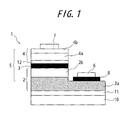
- FIG. 1 schematically shows a cross-sectional structure of a nitride semiconductor light-emitting device according to this invention.
- a nitride semiconductor light-emitting device 1 of the present invention has a semiconductor laminated body 5 including an n-type laminate 2, a light-emitting layer 3 and a p-type laminate 4, and an n-side electrode 6 and a p-side electrode 7, wherein the n-type laminate 2 includes an n-contact layer 2a made of an Al x Ga 1-x N material (0.7 ⁇ x ⁇ 1.0) and an n-clad layer 2b provided on the n-contact layer 2a; and an interlayer 8 made of an Al y Ga 1-y N material (0 ⁇ y ⁇ 0.5) is provided on a partially exposed portion, on the light-emitting layer 3 side, of the n-contact layer 2a.
- the interlayer 8 by an Al y Ga 1-y N material (0 ⁇ y ⁇ 0.3).
- absorption of UV light generated in the light-emitting layer 3 can be significantly reduced by forming the n-contact layer 2a by an Al x Ga 1-x N material (0.7 ⁇ x ⁇ 1.0), as compared with a case forming the n-contact layer 2a by a material having an Al composition ratio (x) of less than 0.7.
- the n-side electrode 6 were to be provided directly on such an n-contact layer 2a as described above, contact resistance between the n-contact layer 2a and the n-side electrode 6 would be significantly high, thereby increasing power loss.
- contact resistance between the n-contact layer 2a and the n-side electrode 6 is effectively decreased by forming the interlayer 8 by an Al y Ga 1-y N material (0 ⁇ y ⁇ 0.5).
- the n-clad layer 2b can be formed, for example, of an Al a Ga 1-a N material (0 ⁇ a ⁇ 1).
- the light-emitting layer 3 can be formed of, for example, an Al b In c Ga 1-b-c N material (0 ⁇ b ⁇ 1, 0 ⁇ c ⁇ 1, 0 ⁇ b+c ⁇ 1).
- the p-type laminate can be formed of, for example, an Al d Ga 1-d N material (0 ⁇ d ⁇ 1). Mg or the like can be used as a p-type dopant, and Si or the like can be used as an n-type dopant.
- thicknesses of the n-contact layer 2a, the n-clad layer 2b, the light-emitting layer 3, the p-clad layer 4a and the p-contact layer 4b, forming the semiconductor laminate body 5, are preferably in the ranges of 1000-5000 nm, 200-500 nm, 20-150 nm, 200-500 nm, and 10-50 nm, respectively. With thicknesses below these ranges, current cannot be diffused sufficiently within the semiconductor layers, while thicknesses larger than these ranges increase the production cost.
- the n-side electrode 6 can be formed, for example, as a metal composite film having a Ti-containing film and an Al-containing film formed on the Ti-containing film. Thickness, shape, and size of each of these films of the n-side electrode can be appropriately selected in accordance with the shape and the size of the light-emitting device.
- the p-side electrode 7 can be formed, for example, as a metal composite film having a Ni-containing film and an Au-containing film formed on the Ni-containing film. Thickness, shape, and size of these films of the p-side electrode can be appropriately selected in accordance with the shape and the size of the light-emitting device.
- interlayer 8 it is preferable to provide another (lower) interlayer formed of an Al z Ga 1-z N material (0.5 ⁇ z ⁇ 0.7) between the interlayer 8 and the n-contact layer 2a because provision of this layer decreases resistance between the interlayer 8 and the n-contact layer 2a. It is more preferable in structural terms to form the interlayer 8 by an Al y Ga 1-y N material (0 ⁇ y ⁇ 0.3) and the lower interlayer by an Al z Ga 1-z N material (0.3 ⁇ z ⁇ 0.7) because then an effect of further reducing contact resistance can be expected.
- Thickness of the interlayer 8 is preferably in the range of 20 nm to 200 nm, and more preferably 50 nm to 100 nm. Thickness of the lower interlayer is preferably in the range of 10 nm to 100 nm, and more preferably 20 nm to 50 nm. In a case where these interlayers are made too thin, the interlayer(s) may diffuse and be mixed with the n-contact layer 2a when contact annealing is conducted, failing to function as an interlayer(s). In a case where the interlayers are made too thick, the production cost will rise because it takes longer time for growth thereof accordingly.
- the nitride semiconductor light-emitting device 1 of the present invention may have a structure in which the n-contact layer 2a is provided on a sapphire substrate 10 by way of a buffer layer 11 made of an AIN material (thickness: 1000 nm to 1500 nm) interposed therebetween, as shown in FIG. 1 .
- an electron blocking layer 12 may be provided between the light-emitting layer 3 and the p-type laminate 4.
- the electron blocking layer 12 serves as a barrier against a quantum well layer of the light-emitting layer 3 and prevents electrons from flowing excessively, thereby enhancing carrier injection efficiency.
- the electron blocking layer 12 may be formed of a p-type Al e Ga 1-e N material (0 ⁇ e ⁇ 1).
- a nitride semiconductor light-emitting device 1 described above can effectively decrease contact resistance between the n-contact layer 2a and the n-side electrode 6, while maintaining satisfactory external quantum efficiency by preventing UV light generated in the light-emitting layer 3 from being absorbed by the n-contact layer 2a.
- the resulting contact resistance between the n-contact layer 2a and the n-side electrode 6 is preferably 10 ⁇ or less and the resulting external quantum efficiency is preferably 0.7 % or more.
- FIG. 2(a) and FIG. 2(b) are cross-sectional views illustrating a process of producing a nitride semiconductor light-emitting device 1 according to the present invention.
- the method of producing a nitride semiconductor light-emitting device includes the steps of: forming a semiconductor laminated body 5 by sequentially growing on a growth substrate 10 an n-type laminate 2 including an n-contact layer 2a and an n-clad layer 2b, a light-emitting layer 3, and a p-type laminate 4 including a p-clad layer 4a and a p-contact layer 4b in this order, as shown in FIG. 2(a) ; forming an interlayer 8 and an n-side electrode 6 on the n-contact layer 2a and forming a p-side electrode 7 on the p-contact layer 4b, as shown in FIG.
- the n-contact layer 2a is formed of an Al x Ga 1-x N material (0.7 ⁇ x ⁇ 1.0), and the interlayer 8 is formed of an Al y Ga 1-y N material (0 ⁇ y ⁇ 0.5). Due to the method including the aforementioned steps, there is obtained a superior effect of being capable of efficiently producing the nitride semiconductor light-emitting device 1, which can effectively decrease contact resistance between the n-contact layer 2a and the n-side electrode 6 while maintaining satisfactory external quantum efficiency by preventing UV light generated in the light-emitting layer 3 from being absorbed by the n-contact layer 2a.
- the semiconductor laminated body 5 is preferably grown epitaxially on the sapphire substrate 10 using, for example, MOCVD.
- MOCVD Use of MOCVD enables layers to be rapidly grown with even thickness.
- the interlayer 8 is preferably formed by partially exposing a portion, on the light-emitting layer 3 side, of the n-contact layer 2a by dry etching and thereafter growing an Al y Ga 1-y N material (0 ⁇ y ⁇ 0.5) on the partially exposed portion of the n-contact layer 2a using MOCVD.
- the Al y Ga 1-y N material deposited on portions other than a part where the n-side electrode 6 is to be formed is removed.
- the n-side electrode 6 can be formed by successively depositing a Ti-containing film and an Al-containing film thereon by vacuum deposition, for example. After this formation process, the n-side electrode 6 is preferably subjected to a predetermined heat treatment in a nitrogen atmosphere in order to bring the n-side electrode 6, the interlayer 8 and the n-contact layer 2a to ohmic contact therebetween.
- the nitride semiconductor light-emitting device 1 according to the present invention can be produced efficiently by using the aforementioned method of producing a nitride semiconductor light-emitting device 1 of the present invention.
- the present invention can achieve particularly high light output power when it is applied to a UV light-emitting device having an emission wavelength of 300 nm or less because UV light generated in a light-emitting layer is then less likely to be absorbed by the n-contact layer.
- a buffer layer 111 AlN material: 1 ⁇ m
- an n-contact layer 102a Si-doped Al 0.7 Ga 0.3 N material: 2 ⁇ m
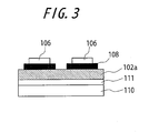
- the interlayer 108 was formed to be 300 ⁇ m ⁇ 300 ⁇ m squares, and the n-side electrodes 106 were formed to be 200 ⁇ m ⁇ 200 ⁇ m squares. Intervals between adjacent squares of the interlayer 108 were set to be 100 ⁇ m.
- the Al composition ratios (%) and the resistance values ( ⁇ ) of the interlayers 108 of Samples 1 to 3 thus formed are shown in Table 1. The resistance values were obtained from the voltage at electric current of 1 mA.
- Samples 1 and 2 each having a relatively small Al composition ratio (y ⁇ 0.3) in the Al y Ga 1-y N material constituting the interlayer 108, exhibit significantly small (not larger than one hundredth) contact resistance values, respectively, as compared with Sample 3 having a relatively large Al composition ratio.
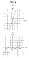
- FIG. 4(a) and FIG. 4(b) are graphs illustrating measurement results of Sample 2 and Sample 3, respectively.
- the X axis represents voltage and the Y-axis represents current.
- FIG. 4(a) the current-voltage characteristics of Sample 2 having Al composition ratio of 30 % are plotted as a straight line, indicating that ohmic contacts had been achieved.
- the current-voltage characteristics of Sample 3 having Al composition raio of 70% are plotted as a curve as shown in FIG. 4(b) , indicating the presence of Schottky contact.
- resistance of a light-emitting device is 1 k ⁇ or less and the current-voltage characteristics thereof are plotted in a straight line. It is understood from the results shown in Table 1, FIG. 4(a) and FIG. 4(b) that good ohmic contact can be obtained and resistance can be greatly reduced when Al composition ratio of the interlayer is in the range of 0 % to 50 % as specified in the present invention.
- a buffer layer 11 AlN material: 1 ⁇ m
- an n-contact layer 2a Si-doped Al 0.7 Ga 0.3 N material: 2 ⁇ m
- an n-clad layer 2b Si-doped Al 0.65 Ga 0.35 N material: 500 nm
- a light-emitting layer 3 Al 0.55 In 0.01 Ga 0.44 N material (10 nm)/Al 0.6 In 0.01 Ga 0.39 N material (15nm) of three-layer multiquantum-well structure, total thickness of 90 nm
- an electron blocking layer 12 Mg-doped Al 0.9 Ga 0.1 N material: 20 nm
- a p-clad layer 4a Mg-doped Al 0.7 Ga 0.3 N material: 200 nm
- a p-contact layer 4b Mg-doped GaN material: 20 nm
- n-contact layer 2a A portion of the n-contact layer 2a was partially exposed by dry etching.
- An interlayer 8 Al 0.3 Ga 0.7 N materials: 50 nm was epitaxially grown on the exposed portion of the n-contact layer 2 by MOCVD. The interlayer 8 was then removed except for a portion on which the n-side electrode 6 was to be formed.
- An n-side electrode 6 Ti/Al was formed on the remained interlayer 8, and a p-side electrode 7 (Ni/Au) was formed on the p-contact layer 4b.
- a nitride semiconductor light-emitting device 1 of Example 2 was formed by the same method as Example 1, except that a lower interlayer (Al 0.3 Ga 0.3 N material: 500 nm) was formed between the n-contact layer 2a and the interlayer 8 in the former.
- a lower interlayer Al 0.3 Ga 0.3 N material: 500 nm
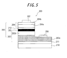
- a nitride semiconductor light-emitting device 200 of Comparative Example 1 was formed by the same method as Example 1, except that the interlayer 8 was not formed in the former, as shown in FIG. 5 .
- a nitride semiconductor light-emitting device 200 of Comparative Example 2 was formed by the same method as Comparative Example 1, except that the n-contact layer 202a was formed by a Si-doped Al 0.3 Ga 0.3 N material in the former.
- Comparative Example 1 lacking an interlayer and having a relatively large Al composition ratio of the n-contact layer, has higher contact resistance between the n-contact layer and the n-side electrode and thus exhibits higher voltage than Examples 1 and 2, and Comparative Example 2. Further, Comparative Example 2, lacking an interlayer and having a relatively small Al composition ratio of the n-contact layer, exhibits relatively low external quantum efficiency due to high amount of absorbed UV light, although voltage drops due to relatively small contact resistance between the n-contact layer and the n-side electrode. In contrast, it is understood that Examples 1 and 2 can each achieve reduction in contact resistance and improvement in external quantum efficiency in a compatible manner.
- nitride semiconductor light-emitting device in which an interlayer made of an Al y Ga 1-y N material (0 ⁇ y ⁇ 0.5) is provided between an n-contact layer made of an Al x Ga 1-x N material (0.7 ⁇ x ⁇ 1.0) and an n-side electrode, of the present invention, contact resistance between the n-contact layer and the n-side electrode is effectively reduced while maintaining satisfactory external quantum efficiency by preventing UV light generated in a light-emitting layer from being absorbed by the n-contact layer. Further, according to the method of producing a nitride semiconductor light-emitting device of the present invention, it is possible to produce such a nitride semiconductor light-emitting device as described above efficiently.
Landscapes
- Led Devices (AREA)
Abstract
Description
- The present invention relates to a nitride semiconductor light-emitting device and a method of manufacturing the same.
- Examples of the characteristics required of a light-emitting device include high external quantum efficiency properties and low resistance properties. A junction barrier is generally formed when a semiconductor is brought into contact with a metal. For example, relatively high contact resistance arises between a semiconductor and an electrode made of a metal material. In a so-called double heterostructure as a basic structure of a light-emitting device, in which both sides of a layer having a relatively narrow band gap (which layer is referred to as a light-emitting layer) is sandwiched between a p-type semiconductor layer and an n-type semiconductor layer each having a wide band gap (which layers are referred to as cladding layers), power loss is caused due to contact resistance arising between a laminate of semiconductor layers and a pair of electrodes mounted thereto when a voltage is applied between the pair of electrodes.
- In order to reduce contact resistance arising between a semiconductor and an electrode, there is a widely known technique of preventing serious power loss from occurring between an electrode and a semiconductor layer by interposing a contact layer formed of a material having a relatively narrow band gap between the electrode and the semiconductor layer to decrease a barrier between the electrode and the semiconductor.
-
JP 2002-141552 JP 2004-335559 - In order to solve the aforementioned problem,
JP 2006-295132 - An object of the present invention is to provide a nitride semiconductor light-emitting device in which contact resistance generated between an n-contact layer and an n-side electrode is effectively reduced while maintaining satisfactory external quantum efficiency, and also provide a method for of efficiently producing the nitride semiconductor light-emitting device. Means for solving the Problem
- The present invention primarily includes following components. (1) A nitride semiconductor light-emitting device having a semiconductor laminated body including an n-type laminate, a light-emitting layer and a p-type laminate, and an n-side electrode and a p-side electrode, characterized in that: the n-type laminate includes an n-contact layer made of an AlxGa1-xN material (0.7 ≤ x ≤ 1.0) and an n-clad layer provided on the n-contact layer; and an interlayer made of an AlyGa1-yN material (0 ≤ y ≤ 0.5) is provided on a partially exposed portion, on the light-emitting layer side, of the n-contact layer.
- (2) The nitride semiconductor light-emitting device of (1) above, further comprising an electron blocking layer between the light-emitting layer and the p-type laminate.
- (3) The nitride semiconductor light-emitting device of (1) or (2) above, in which the resistance between the n-contact layer and the n-side electrode is equal to or less than 10 Ω, and the external quantum efficiency is equal to or higher than 0.70 %.
- (4) A method of producing a nitride semiconductor light-emitting device, comprising the steps of: forming a semiconductor laminated body by sequentially growing on a substrate an n-type laminate including an n-contact layer and an n-clad layer, a light-emitting layer, and a p-type laminate including a p-clad layer and a p-contact layer in this order; forming an interlayer and an n-side electrode on the n-contact layer; and forming a p-side electrode on the p-contact layer, wherein the n-contact layer is formed of an AlxGa1-xN material (0.7 ≤ x ≤ 1.0), and the interlayer is formed of an AlyGa1-yN material (0 ≤ y ≤ 0.5).
- (5) The method of producing a nitride semiconductor light-emitting device of (4) above, further comprising exposing a portion, on the light-emitting layer side, of the n-contact layer by dry etching, and then growing the AlyGa1-yN material on the exposed portion of the n-contact layer by MOCVD.
- According to the nitride semiconductor light-emitting device in which an interlayer made of an AlyGa1-yN material (0 ≤ y ≤ 0.5) is provided between an n-contact layer made of an AlxGa1-xN material (0.7≤x≤1.0) and an n-side electrode, of the present invention, contact resistance between the n-contact layer and the n-side electrode is effectively reduced while maintaining satisfactory external quantum efficiency by preventing UV light generated in a light-emitting layer from being absorbed by the n-contact layer. Further, according to the method of producing a nitride semiconductor light-emitting device of the present invention, it is possible to produce such a nitride semiconductor light-emitting device as described above efficiently.
-
-
FIG.1 is a schematic cross-sectional view illustrating a nitride semiconductor light-emitting device according to the present invention. -
FIGS. 2(a) and 2(b) are schematic cross-sectional views illustrating a process of manufacturing a nitride semiconductor light-emitting device according to the present invention, respectively. -
FIG. 3 is a schematic cross-sectional view illustrating a sample structure for evaluating ohmic properties. -
FIGS. 4(a) and 4(b) are graphs illustrating current-voltage characteristics of Samples, respectively. -
FIG. 5 is a schematic cross-sectional view illustrating a conventional nitride semiconductor light-emitting device. - Next, an embodiment of a nitride semiconductor light-emitting device of the present invention will be described with reference to the accompanying drawings.
FIG. 1 schematically shows a cross-sectional structure of a nitride semiconductor light-emitting device according to this invention. - As shown in
FIG. 1 , a nitride semiconductor light-emitting device 1 of the present invention has a semiconductor laminatedbody 5 including an n-type laminate 2, a light-emittinglayer 3 and a p-type laminate 4, and an n-side electrode 6 and a p-side electrode 7, wherein the n-type laminate 2 includes an n-contact layer 2a made of an AlxGa1-xN material (0.7≤x≤1.0) and an n-clad layer 2b provided on the n-contact layer 2a; and aninterlayer 8 made of an AlyGa1-yN material (0≤y≤0.5) is provided on a partially exposed portion, on the light-emittinglayer 3 side, of the n-contact layer 2a. Due to the aforementioned structure, there are obtained superior effects of effectively reducing contact resistance between the n-contact layer 2a and the n-side electrode 6 while maintaining satisfactory external quantum efficiency by preventing UV light generated in the light-emittinglayer 3 from being absorbed by the n-contact layer 2a. In view of the effect of reducing contact resistance, it is more preferable to form theinterlayer 8 by an AlyGa1-yN material (0≤y≤0.3). - Specifically, absorption of UV light generated in the light-emitting
layer 3 can be significantly reduced by forming the n-contact layer 2a by an AlxGa1-xN material (0.7≤x≤1.0), as compared with a case forming the n-contact layer 2a by a material having an Al composition ratio (x) of less than 0.7. However, if the n-side electrode 6 were to be provided directly on such an n-contact layer 2a as described above, contact resistance between the n-contact layer 2a and the n-side electrode 6 would be significantly high, thereby increasing power loss. - In view of this, in the nitride semiconductor light-
emitting device 1 of the present invention, contact resistance between the n-contact layer 2a and the n-side electrode 6 is effectively decreased by forming theinterlayer 8 by an AlyGa1-yN material (0≤y≤0.5). - The n-
clad layer 2b can be formed, for example, of an AlaGa1-aN material (0≤a≤1). The light-emittinglayer 3 can be formed of, for example, an AlbIncGa1-b-cN material (0≤b≤1, 0≤c≤1, 0≤b+c≤1). The p-type laminate can be formed of, for example, an AldGa1-dN material (0≤d≤1). Mg or the like can be used as a p-type dopant, and Si or the like can be used as an n-type dopant. - Further, thicknesses of the n-
contact layer 2a, the n-clad layer 2b, the light-emittinglayer 3, the p-clad layer 4a and the p-contact layer 4b, forming thesemiconductor laminate body 5, are preferably in the ranges of 1000-5000 nm, 200-500 nm, 20-150 nm, 200-500 nm, and 10-50 nm, respectively. With thicknesses below these ranges, current cannot be diffused sufficiently within the semiconductor layers, while thicknesses larger than these ranges increase the production cost. - The n-
side electrode 6 can be formed, for example, as a metal composite film having a Ti-containing film and an Al-containing film formed on the Ti-containing film. Thickness, shape, and size of each of these films of the n-side electrode can be appropriately selected in accordance with the shape and the size of the light-emitting device. Further, the p-side electrode 7 can be formed, for example, as a metal composite film having a Ni-containing film and an Au-containing film formed on the Ni-containing film. Thickness, shape, and size of these films of the p-side electrode can be appropriately selected in accordance with the shape and the size of the light-emitting device. - Further, although not shown in the drawings, it is preferable to provide another (lower) interlayer formed of an AlzGa1-zN material (0.5 < z < 0.7) between the
interlayer 8 and the n-contact layer 2a because provision of this layer decreases resistance between theinterlayer 8 and the n-contact layer 2a. It is more preferable in structural terms to form theinterlayer 8 by an AlyGa1-yN material (0≤y≤0.3) and the lower interlayer by an AlzGa1-zN material (0.3 < z < 0.7) because then an effect of further reducing contact resistance can be expected. - Thickness of the
interlayer 8 is preferably in the range of 20 nm to 200 nm, and more preferably 50 nm to 100 nm. Thickness of the lower interlayer is preferably in the range of 10 nm to 100 nm, and more preferably 20 nm to 50 nm. In a case where these interlayers are made too thin, the interlayer(s) may diffuse and be mixed with the n-contact layer 2a when contact annealing is conducted, failing to function as an interlayer(s). In a case where the interlayers are made too thick, the production cost will rise because it takes longer time for growth thereof accordingly. - The nitride semiconductor light-
emitting device 1 of the present invention may have a structure in which the n-contact layer 2a is provided on asapphire substrate 10 by way of abuffer layer 11 made of an AIN material (thickness: 1000 nm to 1500 nm) interposed therebetween, as shown inFIG. 1 . - Further, an electron blocking layer 12 (thickness: 5 nm to 50 nm) may be provided between the light-emitting
layer 3 and the p-type laminate 4. Theelectron blocking layer 12 serves as a barrier against a quantum well layer of the light-emittinglayer 3 and prevents electrons from flowing excessively, thereby enhancing carrier injection efficiency. Theelectron blocking layer 12 may be formed of a p-type AleGa1-eN material (0≤e≤1). - A nitride semiconductor light-
emitting device 1 described above can effectively decrease contact resistance between the n-contact layer 2a and the n-side electrode 6, while maintaining satisfactory external quantum efficiency by preventing UV light generated in the light-emittinglayer 3 from being absorbed by the n-contact layer 2a. The resulting contact resistance between the n-contact layer 2a and the n-side electrode 6 is preferably 10 Ω or less and the resulting external quantum efficiency is preferably 0.7 % or more. - Next, an embodiment of a method of producing a nitride semiconductor light-
emitting device 1 of the present invention will be described with reference to the accompanying drawings.FIG. 2(a) and FIG. 2(b) are cross-sectional views illustrating a process of producing a nitride semiconductor light-emitting device 1 according to the present invention. - The method of producing a nitride semiconductor light-emitting device according to the present invention includes the steps of: forming a semiconductor laminated
body 5 by sequentially growing on agrowth substrate 10 an n-type laminate 2 including an n-contact layer 2a and an n-clad layer 2b, a light-emittinglayer 3, and a p-type laminate 4 including a p-clad layer 4a and a p-contact layer 4b in this order, as shown inFIG. 2(a) ; forming aninterlayer 8 and an n-side electrode 6 on the n-contact layer 2a and forming a p-side electrode 7 on the p-contact layer 4b, as shown inFIG. 2(b) , wherein the n-contact layer 2a is formed of an AlxGa1-xN material (0.7≤x≤1.0), and theinterlayer 8 is formed of an AlyGa1-yN material (0≤y≤0.5). Due to the method including the aforementioned steps, there is obtained a superior effect of being capable of efficiently producing the nitride semiconductor light-emitting device 1, which can effectively decrease contact resistance between the n-contact layer 2a and the n-side electrode 6 while maintaining satisfactory external quantum efficiency by preventing UV light generated in the light-emittinglayer 3 from being absorbed by the n-contact layer 2a. - The semiconductor laminated
body 5 is preferably grown epitaxially on thesapphire substrate 10 using, for example, MOCVD. Use of MOCVD enables layers to be rapidly grown with even thickness. - The
interlayer 8 is preferably formed by partially exposing a portion, on the light-emittinglayer 3 side, of the n-contact layer 2a by dry etching and thereafter growing an AlyGa1-yN material (0≤y≤0.5) on the partially exposed portion of the n-contact layer 2a using MOCVD. The AlyGa1-yN material deposited on portions other than a part where the n-side electrode 6 is to be formed is removed. - The n-
side electrode 6 can be formed by successively depositing a Ti-containing film and an Al-containing film thereon by vacuum deposition, for example. After this formation process, the n-side electrode 6 is preferably subjected to a predetermined heat treatment in a nitrogen atmosphere in order to bring the n-side electrode 6, theinterlayer 8 and the n-contact layer 2a to ohmic contact therebetween. - The nitride semiconductor light-emitting
device 1 according to the present invention can be produced efficiently by using the aforementioned method of producing a nitride semiconductor light-emittingdevice 1 of the present invention. The present invention can achieve particularly high light output power when it is applied to a UV light-emitting device having an emission wavelength of 300 nm or less because UV light generated in a light-emitting layer is then less likely to be absorbed by the n-contact layer. - The foregoing descriptions merely illustrate some examples of embodiments of the present invention and various modifications can be made thereto in the scope of accompanying claims.
- (Evaluation of resistance properties and ohmic properties) As shown in
FIG. 3 , a buffer layer 111 (AlN material: 1 µm), an n-contact layer 102a (Si-doped Al0.7Ga0.3N material: 2 µm), and a specific interlayer 108 (AlyGa1-yN materials of three different composition ratios, i.e. y = 0, 0.3, 0.7) were epitaxially grown by MOCVD on asapphire substrate 110. An n-side electrodes 106 (Ti/Al = 20 nm/ 200 nm) were then formed thereon by vacuum deposition. Theinterlayer 108 was formed to be 300 µm × 300 µm squares, and the n-side electrodes 106 were formed to be 200 µm × 200 µm squares. Intervals between adjacent squares of theinterlayer 108 were set to be 100 µm. The Al composition ratios (%) and the resistance values (Ω) of theinterlayers 108 ofSamples 1 to 3 thus formed are shown in Table 1. The resistance values were obtained from the voltage at electric current of 1 mA. -
[Table 1] Al composition ratio (%) Resistance value (Ω) Sample 10 12 Sample 230 9 Sample 370 3000 - As shown in Table 1,
Samples interlayer 108, exhibit significantly small (not larger than one hundredth) contact resistance values, respectively, as compared withSample 3 having a relatively large Al composition ratio. - Further, current-voltage characteristics were measured for these samples by using a curve tracer.
FIG. 4(a) and FIG. 4(b) are graphs illustrating measurement results ofSample 2 andSample 3, respectively. The X axis represents voltage and the Y-axis represents current. As shown inFIG. 4(a) , the current-voltage characteristics ofSample 2 having Al composition ratio of 30 % are plotted as a straight line, indicating that ohmic contacts had been achieved. In contrast, the current-voltage characteristics ofSample 3 having Al composition raio of 70% are plotted as a curve as shown inFIG. 4(b) , indicating the presence of Schottky contact. - In general, it is desirable that resistance of a light-emitting device is 1 kΩ or less and the current-voltage characteristics thereof are plotted in a straight line. It is understood from the results shown in Table 1,
FIG. 4(a) and FIG. 4(b) that good ohmic contact can be obtained and resistance can be greatly reduced when Al composition ratio of the interlayer is in the range of 0 % to 50 % as specified in the present invention. - A buffer layer 11 (AlN material: 1 µm), an n-
contact layer 2a (Si-doped Al0.7Ga0.3N material: 2 µm), an n-cladlayer 2b (Si-doped Al0.65Ga0.35N material: 500 nm), a light-emitting layer 3 (Al0.55In0.01Ga0.44N material (10 nm)/Al0.6In0.01Ga0.39N material (15nm) of three-layer multiquantum-well structure, total thickness of 90 nm), an electron blocking layer 12 (Mg-doped Al0.9Ga0.1N material: 20 nm), a p-cladlayer 4a (Mg-doped Al0.7Ga0.3N material: 200 nm), and a p-contact layer 4b (Mg-doped GaN material: 20 nm) were epitaxially grown in this order successively on asapphire substrate 10 by MOCVD, as shown inFIG. 1 . A portion of the n-contact layer 2a was partially exposed by dry etching. An interlayer 8 (Al0.3Ga0.7N materials: 50 nm) was epitaxially grown on the exposed portion of the n-contact layer 2 by MOCVD. Theinterlayer 8 was then removed except for a portion on which the n-side electrode 6 was to be formed. An n-side electrode 6 (Ti/Al) was formed on the remainedinterlayer 8, and a p-side electrode 7 (Ni/Au) was formed on the p-contact layer 4b. Thereafter, heat treatment was carried out in nitrogen atmosphere, so that the n-side electrode 6 and the n-contact layer 2a were brought into ohmic contact, whereby the nitride semiconductor light-emittingdevice 1 of Example 1 according to the present invention was formed. - A nitride semiconductor light-emitting
device 1 of Example 2 was formed by the same method as Example 1, except that a lower interlayer (Al0.3Ga0.3N material: 500 nm) was formed between the n-contact layer 2a and theinterlayer 8 in the former. - A nitride semiconductor light-emitting
device 200 of Comparative Example 1 was formed by the same method as Example 1, except that theinterlayer 8 was not formed in the former, as shown inFIG. 5 . - A nitride semiconductor light-emitting
device 200 of Comparative Example 2 was formed by the same method as Comparative Example 1, except that the n-contact layer 202a was formed by a Si-doped Al0.3Ga0.3N material in the former. - Each of the nitride semiconductor light-emitting devices thus formed was assembled into a flip-chip package. Voltage Vf (V) and light output power Po (mW) at electric current of 20 mA were measured, respectively, using an integrating sphere. The measurement results, as well as the values of external quantum efficiency calculated from the formula below, are shown in Table 2.

-
[Table 2] Voltage Vf (V) Light output power Po (mW) External quantum efficiency (%) Example 1 11.14 0.71 0.76 Example 2 10.40 0.76 0.81 Comparative Example 1 14.85 0.54 0.58 Comparative Example 2 11.73 0.45 0.48 - As shown in table 2, Comparative Example 1, lacking an interlayer and having a relatively large Al composition ratio of the n-contact layer, has higher contact resistance between the n-contact layer and the n-side electrode and thus exhibits higher voltage than Examples 1 and 2, and Comparative Example 2. Further, Comparative Example 2, lacking an interlayer and having a relatively small Al composition ratio of the n-contact layer, exhibits relatively low external quantum efficiency due to high amount of absorbed UV light, although voltage drops due to relatively small contact resistance between the n-contact layer and the n-side electrode. In contrast, it is understood that Examples 1 and 2 can each achieve reduction in contact resistance and improvement in external quantum efficiency in a compatible manner.
- According to the nitride semiconductor light-emitting device in which an interlayer made of an AlyGa1-yN material (0≤y≤0.5) is provided between an n-contact layer made of an AlxGa1-xN material (0.7≤x≤1.0) and an n-side electrode, of the present invention, contact resistance between the n-contact layer and the n-side electrode is effectively reduced while maintaining satisfactory external quantum efficiency by preventing UV light generated in a light-emitting layer from being absorbed by the n-contact layer. Further, according to the method of producing a nitride semiconductor light-emitting device of the present invention, it is possible to produce such a nitride semiconductor light-emitting device as described above efficiently.
-
- 1
- Nitride semiconductor light-emitting device
- 2
- N-type laminate
- 2a
- N-contact layer
- 2n
- N-clad layer
- 3
- Light-emitting layer
- 4
- P-type laminate
- 4a
- P-clad layer
- 4b
- P-contact layer
- 5
- Semiconductor laminated body
- 6
- N-side electrode
- 7
- P-side electrode
- 8
- Interlayer
- 10
- Substrate
- 11
- Buffer layer
- 12
- Electron blocking layer
- 102a
- N-contact layer
- 106
- N-side electrode
- 108
- Interlayer
- 110
- Sapphire substrate
- 111
- Buffer layer.
Claims (5)
- A nitride semiconductor light-emitting device having a semiconductor laminated body including an n-type laminate, a light-emitting layer and a p-type laminate, and an n-side electrode and a p-side electrode, characterized in that:the n-type laminate includes an n-contact layer made of an AlxGa1-xN material (0.7≤x≤1.0) and an n-clad layer provided on the n-contact layer; andan interlayer made of an AlyGa1-yN material (0≤y≤0.5) is provided on a partially exposed portion, on the light-emitting layer side, of the n-contact layer.
- The nitride semiconductor light-emitting device of claim 1, further comprising an electron blocking layer between the light-emitting layer and the p-type laminate.
- The nitride semiconductor light-emitting device of claim 1 or 2, wherein the resistance between the n-contact layer and the n-side electrode is equal to or less than 10 Ω, and the external quantum efficiency is equal to or higher than 0.70 %.
- A method of producing a nitride semiconductor light-emitting device, comprising the steps of:forming a semiconductor laminated body by sequentially growing on a substrate an n-type laminate including an n-contact layer and an n-clad layer, a light-emitting layer, and a p-type laminate including a p-clad layer and a p-contact layer in this order;forming an interlayer and an n-side electrode on the n-contact layer; andforming a p-side electrode on the p-contact layer,wherein the n-contact layer is formed of an AlxGa1-xN material (0.7≤x≤ 1.0), and the interlayer is formed of an AlyGa1-yN material (0≤y≤0.5).
- The method of producing a nitride semiconductor light-emitting device of claim 4, further comprising exposing a portion, on the light-emitting layer side, of the n-contact layer by dry etching, and then growing the AlyGa1-yN material on the exposed portion of the n-contact layer by MOCVD.
Applications Claiming Priority (2)
| Application Number | Priority Date | Filing Date | Title |
|---|---|---|---|
| JP2009003933A JP5352248B2 (en) | 2009-01-09 | 2009-01-09 | Nitride semiconductor light emitting device and manufacturing method thereof |
| PCT/JP2009/007214 WO2010079567A1 (en) | 2009-01-09 | 2009-12-24 | Nitride semiconductor light-emitting element, and method for manufacturing same |
Publications (3)
| Publication Number | Publication Date |
|---|---|
| EP2378574A1 true EP2378574A1 (en) | 2011-10-19 |
| EP2378574A4 EP2378574A4 (en) | 2013-04-24 |
| EP2378574B1 EP2378574B1 (en) | 2014-06-04 |
Family
ID=42316346
Family Applications (1)
| Application Number | Title | Priority Date | Filing Date |
|---|---|---|---|
| EP09837457.2A Active EP2378574B1 (en) | 2009-01-09 | 2009-12-24 | Nitride semiconductor light-emitting element, and method for manufacturing same |
Country Status (6)
| Country | Link |
|---|---|
| US (1) | US8330168B2 (en) |
| EP (1) | EP2378574B1 (en) |
| JP (1) | JP5352248B2 (en) |
| KR (1) | KR101343198B1 (en) |
| CN (1) | CN102349167B (en) |
| WO (1) | WO2010079567A1 (en) |
Cited By (1)
| Publication number | Priority date | Publication date | Assignee | Title |
|---|---|---|---|---|
| WO2019042746A1 (en) * | 2017-08-30 | 2019-03-07 | Osram Opto Semiconductors Gmbh | OPTOELECTRONIC SEMICONDUCTOR ELEMENT |
Families Citing this family (19)
| Publication number | Priority date | Publication date | Assignee | Title |
|---|---|---|---|---|
| JP5594530B2 (en) * | 2010-10-21 | 2014-09-24 | 創光科学株式会社 | Nitride semiconductor ultraviolet light emitting device |
| JP2014154597A (en) * | 2013-02-05 | 2014-08-25 | Tokuyama Corp | Nitride semiconductor light-emitting element |
| US20160005919A1 (en) * | 2013-02-05 | 2016-01-07 | Tokuyama Corporation | Nitride semiconductor light emitting device |
| JP2015002290A (en) * | 2013-06-17 | 2015-01-05 | ウシオ電機株式会社 | Composition for transparent conductive film, transparent electrode, semiconductor light-emitting element, and solar cell |
| WO2015042552A1 (en) | 2013-09-23 | 2015-03-26 | Sensor Electronic Technology , Inc. | Group iii nitride heterostructure for optoelectronic device |
| JP6330604B2 (en) * | 2014-09-24 | 2018-05-30 | 日亜化学工業株式会社 | Semiconductor light emitting device |
| JP5953447B1 (en) | 2015-02-05 | 2016-07-20 | Dowaエレクトロニクス株式会社 | Group III nitride semiconductor light emitting device and method of manufacturing the same |
| KR102329719B1 (en) * | 2015-02-23 | 2021-11-23 | 쑤저우 레킨 세미컨덕터 컴퍼니 리미티드 | Light emitting device and light unit having thereof |
| US10290771B2 (en) | 2016-04-20 | 2019-05-14 | Dowa Electronics Materials Co., Ltd. | Group III nitride semiconductor light emitting device and method for manufacture the same |
| JP6730082B2 (en) * | 2016-05-02 | 2020-07-29 | 日機装株式会社 | Method for manufacturing deep ultraviolet light emitting device |
| WO2017221863A1 (en) | 2016-06-24 | 2017-12-28 | スタンレー電気株式会社 | Group iii nitride laminate and vertical semiconductor device provided with said laminate |
| WO2019203322A1 (en) | 2018-04-20 | 2019-10-24 | Dowaエレクトロニクス株式会社 | Deep ultraviolet light-emitting element |
| DE102018120490A1 (en) * | 2018-08-22 | 2020-02-27 | Osram Opto Semiconductors Gmbh | OPTOELECTRONIC SEMICONDUCTOR COMPONENT WITH A SEMICONDUCTOR CONTACT LAYER AND METHOD FOR PRODUCING THE OPTOELECTRONIC SEMICONDUCTOR COMPONENT |
| EP4107792A4 (en) * | 2020-03-20 | 2024-03-27 | Sensor Electronic Technology, Inc. | OPTOELECTRONIC DEVICE WITH REDUCED OPTICAL LOSS |
| CN112652691A (en) * | 2020-12-30 | 2021-04-13 | 深圳第三代半导体研究院 | Light emitting diode and manufacturing method thereof |
| CN120475829A (en) * | 2021-03-23 | 2025-08-12 | 隆达电子股份有限公司 | Light emitting diode structure |
| JP7544004B2 (en) * | 2021-08-30 | 2024-09-03 | 豊田合成株式会社 | Light emitting element |
| EP4401158A4 (en) | 2021-09-09 | 2025-11-12 | Univ Mie | Group III nitride light emission component, group III nitride epitaxial wafer and method for manufacturing a group III nitride light emission component |
| CN115714156A (en) * | 2022-11-24 | 2023-02-24 | 苏州紫灿科技有限公司 | Deep ultraviolet light-emitting diode |
Family Cites Families (14)
| Publication number | Priority date | Publication date | Assignee | Title |
|---|---|---|---|---|
| JP3502651B2 (en) * | 1993-02-08 | 2004-03-02 | トリクイント セミコンダクター テキサス、エルピー | Electrode formation method |
| EP0632510B1 (en) * | 1993-06-08 | 2001-10-31 | Rohm Co., Ltd. | Semiconductor light emitting device and its manufacturing method |
| JP2002141552A (en) | 2000-10-31 | 2002-05-17 | Ricoh Co Ltd | Group III nitride semiconductor, semiconductor substrate, laser and semiconductor device using the semiconductor |
| JP2003142728A (en) * | 2001-11-02 | 2003-05-16 | Sharp Corp | Method for manufacturing semiconductor light emitting device |
| US20060006375A1 (en) * | 2003-04-14 | 2006-01-12 | Chen Ou | Light Mixing LED |
| JP2004335559A (en) | 2003-04-30 | 2004-11-25 | Nichia Chem Ind Ltd | Semiconductor device using group III nitride substrate |
| JP2006066556A (en) * | 2004-08-25 | 2006-03-09 | Nippon Telegr & Teleph Corp <Ntt> | Nitride semiconductor device and manufacturing method thereof |
| JP2006245162A (en) * | 2005-03-02 | 2006-09-14 | Osaka Gas Co Ltd | Nitride semiconductor light-emitting element |
| JP4653671B2 (en) | 2005-03-14 | 2011-03-16 | 株式会社東芝 | Light emitting device |
| KR100878433B1 (en) * | 2005-05-18 | 2009-01-13 | 삼성전기주식회사 | Method for manufacturing ohmic contact layer of light emitting device and method for manufacturing light emitting device using same |
| JP4183719B2 (en) * | 2005-06-29 | 2008-11-19 | 三洋電機株式会社 | Nitride semiconductor devices |
| JP2008140917A (en) * | 2006-11-30 | 2008-06-19 | Sumitomo Electric Ind Ltd | Nitride semiconductor light emitting device |
| JP2008171941A (en) * | 2007-01-10 | 2008-07-24 | Ngk Insulators Ltd | Light emitting element |
| KR20090022701A (en) * | 2007-08-31 | 2009-03-04 | 엘지이노텍 주식회사 | Semiconductor light emitting device and manufacturing method thereof |
-
2009
- 2009-01-09 JP JP2009003933A patent/JP5352248B2/en active Active
- 2009-12-24 EP EP09837457.2A patent/EP2378574B1/en active Active
- 2009-12-24 KR KR1020117017742A patent/KR101343198B1/en active Active
- 2009-12-24 US US13/143,874 patent/US8330168B2/en active Active
- 2009-12-24 WO PCT/JP2009/007214 patent/WO2010079567A1/en not_active Ceased
- 2009-12-24 CN CN2009801580020A patent/CN102349167B/en active Active
Cited By (2)
| Publication number | Priority date | Publication date | Assignee | Title |
|---|---|---|---|---|
| WO2019042746A1 (en) * | 2017-08-30 | 2019-03-07 | Osram Opto Semiconductors Gmbh | OPTOELECTRONIC SEMICONDUCTOR ELEMENT |
| US11527865B2 (en) | 2017-08-30 | 2022-12-13 | Osram Oled Gmbh | Optoelectronic semiconductor component |
Also Published As
| Publication number | Publication date |
|---|---|
| US8330168B2 (en) | 2012-12-11 |
| EP2378574B1 (en) | 2014-06-04 |
| KR101343198B1 (en) | 2013-12-19 |
| EP2378574A4 (en) | 2013-04-24 |
| US20110266553A1 (en) | 2011-11-03 |
| KR20110106425A (en) | 2011-09-28 |
| JP2010161311A (en) | 2010-07-22 |
| CN102349167A (en) | 2012-02-08 |
| JP5352248B2 (en) | 2013-11-27 |
| WO2010079567A1 (en) | 2010-07-15 |
| CN102349167B (en) | 2013-09-04 |
Similar Documents
| Publication | Publication Date | Title |
|---|---|---|
| EP2378574B1 (en) | Nitride semiconductor light-emitting element, and method for manufacturing same | |
| JP5045248B2 (en) | Semiconductor light emitting device and manufacturing method thereof | |
| US8569738B2 (en) | Semiconductor light emitting device, wafer, method for manufacturing semiconductor light emitting device, and method for manufacturing wafer | |
| JP6940664B2 (en) | Deep ultraviolet light emitting device and its manufacturing method | |
| US20200235260A1 (en) | Deep ultraviolet light-emitting device and method of manufacturing same | |
| US6712478B2 (en) | Light emitting diode | |
| US20090321745A1 (en) | Semiconductor light-emitting device | |
| US7196347B2 (en) | Semiconductor light emitting device | |
| US20030209717A1 (en) | Semiconductor light-emitting element and method of fabrication thereof | |
| CA2487149A1 (en) | Group iii nitride led with undoped cladding layer and multiple quantum well | |
| KR102426467B1 (en) | Method for manufacturing semiconductor optical device and intermediate for semiconductor optical device | |
| US8044439B2 (en) | Light-emitting device and manufacturing method of the same | |
| JP4320653B2 (en) | Semiconductor light emitting device | |
| US8754528B2 (en) | Semiconductor device | |
| JP5289791B2 (en) | Nitride semiconductor light emitting device and manufacturing method thereof | |
| JP2020120114A (en) | Method of manufacturing reflective electrode for deep ultraviolet light-emitting element, method of manufacturing deep ultraviolet light-emitting element, and deep ultraviolet light-emitting element | |
| JP4284103B2 (en) | Oxide semiconductor light emitting device | |
| JP4320654B2 (en) | Semiconductor light emitting device | |
| JP7413599B1 (en) | III-V group compound semiconductor light emitting device and method for manufacturing the III-V group compound semiconductor light emitting device | |
| CN119521865A (en) | Ultra-thin tunnel junction deep ultraviolet LED chip and manufacturing method thereof | |
| JP2007311375A (en) | A manufacturing method of a p-type III-V compound semiconductor and a manufacturing method of a light emitting element. |
Legal Events
| Date | Code | Title | Description |
|---|---|---|---|
| PUAI | Public reference made under article 153(3) epc to a published international application that has entered the european phase |
Free format text: ORIGINAL CODE: 0009012 |
|
| 17P | Request for examination filed |
Effective date: 20110714 |
|
| AK | Designated contracting states |
Kind code of ref document: A1 Designated state(s): AT BE BG CH CY CZ DE DK EE ES FI FR GB GR HR HU IE IS IT LI LT LU LV MC MK MT NL NO PL PT RO SE SI SK SM TR |
|
| DAX | Request for extension of the european patent (deleted) | ||
| A4 | Supplementary search report drawn up and despatched |
Effective date: 20130321 |
|
| RIC1 | Information provided on ipc code assigned before grant |
Ipc: H01L 33/40 20100101AFI20130315BHEP Ipc: H01L 33/32 20100101ALI20130315BHEP Ipc: H01L 33/02 20100101ALI20130315BHEP |
|
| GRAP | Despatch of communication of intention to grant a patent |
Free format text: ORIGINAL CODE: EPIDOSNIGR1 |
|
| INTG | Intention to grant announced |
Effective date: 20140212 |
|
| GRAS | Grant fee paid |
Free format text: ORIGINAL CODE: EPIDOSNIGR3 |
|
| GRAA | (expected) grant |
Free format text: ORIGINAL CODE: 0009210 |
|
| AK | Designated contracting states |
Kind code of ref document: B1 Designated state(s): AT BE BG CH CY CZ DE DK EE ES FI FR GB GR HR HU IE IS IT LI LT LU LV MC MK MT NL NO PL PT RO SE SI SK SM TR |
|
| REG | Reference to a national code |
Ref country code: GB Ref legal event code: FG4D |
|
| REG | Reference to a national code |
Ref country code: CH Ref legal event code: EP |
|
| REG | Reference to a national code |
Ref country code: AT Ref legal event code: REF Ref document number: 671518 Country of ref document: AT Kind code of ref document: T Effective date: 20140615 |
|
| REG | Reference to a national code |
Ref country code: IE Ref legal event code: FG4D |
|
| REG | Reference to a national code |
Ref country code: DE Ref legal event code: R096 Ref document number: 602009024529 Country of ref document: DE Effective date: 20140717 |
|
| REG | Reference to a national code |
Ref country code: AT Ref legal event code: MK05 Ref document number: 671518 Country of ref document: AT Kind code of ref document: T Effective date: 20140604 |
|
| REG | Reference to a national code |
Ref country code: NL Ref legal event code: VDEP Effective date: 20140604 |
|
| PG25 | Lapsed in a contracting state [announced via postgrant information from national office to epo] |
Ref country code: GR Free format text: LAPSE BECAUSE OF FAILURE TO SUBMIT A TRANSLATION OF THE DESCRIPTION OR TO PAY THE FEE WITHIN THE PRESCRIBED TIME-LIMIT Effective date: 20140905 Ref country code: CY Free format text: LAPSE BECAUSE OF FAILURE TO SUBMIT A TRANSLATION OF THE DESCRIPTION OR TO PAY THE FEE WITHIN THE PRESCRIBED TIME-LIMIT Effective date: 20140604 Ref country code: NO Free format text: LAPSE BECAUSE OF FAILURE TO SUBMIT A TRANSLATION OF THE DESCRIPTION OR TO PAY THE FEE WITHIN THE PRESCRIBED TIME-LIMIT Effective date: 20140904 Ref country code: FI Free format text: LAPSE BECAUSE OF FAILURE TO SUBMIT A TRANSLATION OF THE DESCRIPTION OR TO PAY THE FEE WITHIN THE PRESCRIBED TIME-LIMIT Effective date: 20140604 Ref country code: LT Free format text: LAPSE BECAUSE OF FAILURE TO SUBMIT A TRANSLATION OF THE DESCRIPTION OR TO PAY THE FEE WITHIN THE PRESCRIBED TIME-LIMIT Effective date: 20140604 |
|
| REG | Reference to a national code |
Ref country code: LT Ref legal event code: MG4D |
|
| PG25 | Lapsed in a contracting state [announced via postgrant information from national office to epo] |
Ref country code: LV Free format text: LAPSE BECAUSE OF FAILURE TO SUBMIT A TRANSLATION OF THE DESCRIPTION OR TO PAY THE FEE WITHIN THE PRESCRIBED TIME-LIMIT Effective date: 20140604 Ref country code: SE Free format text: LAPSE BECAUSE OF FAILURE TO SUBMIT A TRANSLATION OF THE DESCRIPTION OR TO PAY THE FEE WITHIN THE PRESCRIBED TIME-LIMIT Effective date: 20140604 Ref country code: AT Free format text: LAPSE BECAUSE OF FAILURE TO SUBMIT A TRANSLATION OF THE DESCRIPTION OR TO PAY THE FEE WITHIN THE PRESCRIBED TIME-LIMIT Effective date: 20140604 Ref country code: HR Free format text: LAPSE BECAUSE OF FAILURE TO SUBMIT A TRANSLATION OF THE DESCRIPTION OR TO PAY THE FEE WITHIN THE PRESCRIBED TIME-LIMIT Effective date: 20140604 |
|
| PG25 | Lapsed in a contracting state [announced via postgrant information from national office to epo] |
Ref country code: RO Free format text: LAPSE BECAUSE OF FAILURE TO SUBMIT A TRANSLATION OF THE DESCRIPTION OR TO PAY THE FEE WITHIN THE PRESCRIBED TIME-LIMIT Effective date: 20140604 Ref country code: EE Free format text: LAPSE BECAUSE OF FAILURE TO SUBMIT A TRANSLATION OF THE DESCRIPTION OR TO PAY THE FEE WITHIN THE PRESCRIBED TIME-LIMIT Effective date: 20140604 Ref country code: ES Free format text: LAPSE BECAUSE OF FAILURE TO SUBMIT A TRANSLATION OF THE DESCRIPTION OR TO PAY THE FEE WITHIN THE PRESCRIBED TIME-LIMIT Effective date: 20140604 Ref country code: SK Free format text: LAPSE BECAUSE OF FAILURE TO SUBMIT A TRANSLATION OF THE DESCRIPTION OR TO PAY THE FEE WITHIN THE PRESCRIBED TIME-LIMIT Effective date: 20140604 Ref country code: CZ Free format text: LAPSE BECAUSE OF FAILURE TO SUBMIT A TRANSLATION OF THE DESCRIPTION OR TO PAY THE FEE WITHIN THE PRESCRIBED TIME-LIMIT Effective date: 20140604 Ref country code: PT Free format text: LAPSE BECAUSE OF FAILURE TO SUBMIT A TRANSLATION OF THE DESCRIPTION OR TO PAY THE FEE WITHIN THE PRESCRIBED TIME-LIMIT Effective date: 20141006 |
|
| PG25 | Lapsed in a contracting state [announced via postgrant information from national office to epo] |
Ref country code: NL Free format text: LAPSE BECAUSE OF FAILURE TO SUBMIT A TRANSLATION OF THE DESCRIPTION OR TO PAY THE FEE WITHIN THE PRESCRIBED TIME-LIMIT Effective date: 20140604 Ref country code: IS Free format text: LAPSE BECAUSE OF FAILURE TO SUBMIT A TRANSLATION OF THE DESCRIPTION OR TO PAY THE FEE WITHIN THE PRESCRIBED TIME-LIMIT Effective date: 20141004 Ref country code: PL Free format text: LAPSE BECAUSE OF FAILURE TO SUBMIT A TRANSLATION OF THE DESCRIPTION OR TO PAY THE FEE WITHIN THE PRESCRIBED TIME-LIMIT Effective date: 20140604 |
|
| REG | Reference to a national code |
Ref country code: DE Ref legal event code: R097 Ref document number: 602009024529 Country of ref document: DE |
|
| PLBE | No opposition filed within time limit |
Free format text: ORIGINAL CODE: 0009261 |
|
| STAA | Information on the status of an ep patent application or granted ep patent |
Free format text: STATUS: NO OPPOSITION FILED WITHIN TIME LIMIT |
|
| PG25 | Lapsed in a contracting state [announced via postgrant information from national office to epo] |
Ref country code: IT Free format text: LAPSE BECAUSE OF FAILURE TO SUBMIT A TRANSLATION OF THE DESCRIPTION OR TO PAY THE FEE WITHIN THE PRESCRIBED TIME-LIMIT Effective date: 20140604 Ref country code: DK Free format text: LAPSE BECAUSE OF FAILURE TO SUBMIT A TRANSLATION OF THE DESCRIPTION OR TO PAY THE FEE WITHIN THE PRESCRIBED TIME-LIMIT Effective date: 20140604 |
|
| 26N | No opposition filed |
Effective date: 20150305 |
|
| REG | Reference to a national code |
Ref country code: DE Ref legal event code: R097 Ref document number: 602009024529 Country of ref document: DE Effective date: 20150305 |
|
| PG25 | Lapsed in a contracting state [announced via postgrant information from national office to epo] |
Ref country code: BE Free format text: LAPSE BECAUSE OF FAILURE TO SUBMIT A TRANSLATION OF THE DESCRIPTION OR TO PAY THE FEE WITHIN THE PRESCRIBED TIME-LIMIT Effective date: 20140604 |
|
| PG25 | Lapsed in a contracting state [announced via postgrant information from national office to epo] |
Ref country code: SI Free format text: LAPSE BECAUSE OF FAILURE TO SUBMIT A TRANSLATION OF THE DESCRIPTION OR TO PAY THE FEE WITHIN THE PRESCRIBED TIME-LIMIT Effective date: 20140604 Ref country code: LU Free format text: LAPSE BECAUSE OF FAILURE TO SUBMIT A TRANSLATION OF THE DESCRIPTION OR TO PAY THE FEE WITHIN THE PRESCRIBED TIME-LIMIT Effective date: 20141224 |
|
| REG | Reference to a national code |
Ref country code: CH Ref legal event code: PL |
|
| REG | Reference to a national code |
Ref country code: IE Ref legal event code: MM4A |
|
| REG | Reference to a national code |
Ref country code: FR Ref legal event code: ST Effective date: 20150831 |
|
| PG25 | Lapsed in a contracting state [announced via postgrant information from national office to epo] |
Ref country code: CH Free format text: LAPSE BECAUSE OF NON-PAYMENT OF DUE FEES Effective date: 20141231 Ref country code: IE Free format text: LAPSE BECAUSE OF NON-PAYMENT OF DUE FEES Effective date: 20141224 Ref country code: LI Free format text: LAPSE BECAUSE OF NON-PAYMENT OF DUE FEES Effective date: 20141231 |
|
| PG25 | Lapsed in a contracting state [announced via postgrant information from national office to epo] |
Ref country code: FR Free format text: LAPSE BECAUSE OF NON-PAYMENT OF DUE FEES Effective date: 20141231 |
|
| PG25 | Lapsed in a contracting state [announced via postgrant information from national office to epo] |
Ref country code: SM Free format text: LAPSE BECAUSE OF FAILURE TO SUBMIT A TRANSLATION OF THE DESCRIPTION OR TO PAY THE FEE WITHIN THE PRESCRIBED TIME-LIMIT Effective date: 20140604 |
|
| PG25 | Lapsed in a contracting state [announced via postgrant information from national office to epo] |
Ref country code: MC Free format text: LAPSE BECAUSE OF FAILURE TO SUBMIT A TRANSLATION OF THE DESCRIPTION OR TO PAY THE FEE WITHIN THE PRESCRIBED TIME-LIMIT Effective date: 20140604 |
|
| PG25 | Lapsed in a contracting state [announced via postgrant information from national office to epo] |
Ref country code: BG Free format text: LAPSE BECAUSE OF FAILURE TO SUBMIT A TRANSLATION OF THE DESCRIPTION OR TO PAY THE FEE WITHIN THE PRESCRIBED TIME-LIMIT Effective date: 20140604 |
|
| PG25 | Lapsed in a contracting state [announced via postgrant information from national office to epo] |
Ref country code: HU Free format text: LAPSE BECAUSE OF FAILURE TO SUBMIT A TRANSLATION OF THE DESCRIPTION OR TO PAY THE FEE WITHIN THE PRESCRIBED TIME-LIMIT; INVALID AB INITIO Effective date: 20091224 Ref country code: MT Free format text: LAPSE BECAUSE OF FAILURE TO SUBMIT A TRANSLATION OF THE DESCRIPTION OR TO PAY THE FEE WITHIN THE PRESCRIBED TIME-LIMIT Effective date: 20140604 Ref country code: TR Free format text: LAPSE BECAUSE OF FAILURE TO SUBMIT A TRANSLATION OF THE DESCRIPTION OR TO PAY THE FEE WITHIN THE PRESCRIBED TIME-LIMIT Effective date: 20140604 |
|
| PG25 | Lapsed in a contracting state [announced via postgrant information from national office to epo] |
Ref country code: MK Free format text: LAPSE BECAUSE OF FAILURE TO SUBMIT A TRANSLATION OF THE DESCRIPTION OR TO PAY THE FEE WITHIN THE PRESCRIBED TIME-LIMIT Effective date: 20140604 |
|
| P01 | Opt-out of the competence of the unified patent court (upc) registered |
Effective date: 20230420 |
|
| REG | Reference to a national code |
Ref country code: DE Ref legal event code: R079 Ref document number: 602009024529 Country of ref document: DE Free format text: PREVIOUS MAIN CLASS: H01L0033400000 Ipc: H10H0020832000 |
|
| PGFP | Annual fee paid to national office [announced via postgrant information from national office to epo] |
Ref country code: DE Payment date: 20251028 Year of fee payment: 17 |
|
| PGFP | Annual fee paid to national office [announced via postgrant information from national office to epo] |
Ref country code: GB Payment date: 20251030 Year of fee payment: 17 |