EP2378555A2 - Light emitting device and light emitting device package - Google Patents
Light emitting device and light emitting device package Download PDFInfo
- Publication number
- EP2378555A2 EP2378555A2 EP11157948A EP11157948A EP2378555A2 EP 2378555 A2 EP2378555 A2 EP 2378555A2 EP 11157948 A EP11157948 A EP 11157948A EP 11157948 A EP11157948 A EP 11157948A EP 2378555 A2 EP2378555 A2 EP 2378555A2
- Authority
- EP
- European Patent Office
- Prior art keywords
- light emitting
- emitting device
- electrode
- layer
- semiconductor layer
- Prior art date
- Legal status (The legal status is an assumption and is not a legal conclusion. Google has not performed a legal analysis and makes no representation as to the accuracy of the status listed.)
- Granted
Links
Images


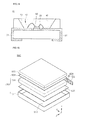

Classifications
-
- H—ELECTRICITY
- H10—SEMICONDUCTOR DEVICES; ELECTRIC SOLID-STATE DEVICES NOT OTHERWISE PROVIDED FOR
- H10H—INORGANIC LIGHT-EMITTING SEMICONDUCTOR DEVICES HAVING POTENTIAL BARRIERS
- H10H29/00—Integrated devices, or assemblies of multiple devices, comprising at least one light-emitting semiconductor element covered by group H10H20/00
- H10H29/10—Integrated devices comprising at least one light-emitting semiconductor component covered by group H10H20/00
-
- H—ELECTRICITY
- H10—SEMICONDUCTOR DEVICES; ELECTRIC SOLID-STATE DEVICES NOT OTHERWISE PROVIDED FOR
- H10D—INORGANIC ELECTRIC SEMICONDUCTOR DEVICES
- H10D30/00—Field-effect transistors [FET]
- H10D30/60—Insulated-gate field-effect transistors [IGFET]
-
- H—ELECTRICITY
- H10—SEMICONDUCTOR DEVICES; ELECTRIC SOLID-STATE DEVICES NOT OTHERWISE PROVIDED FOR
- H10H—INORGANIC LIGHT-EMITTING SEMICONDUCTOR DEVICES HAVING POTENTIAL BARRIERS
- H10H20/00—Individual inorganic light-emitting semiconductor devices having potential barriers, e.g. light-emitting diodes [LED]
- H10H20/80—Constructional details
- H10H20/83—Electrodes
- H10H20/831—Electrodes characterised by their shape
-
- H—ELECTRICITY
- H10—SEMICONDUCTOR DEVICES; ELECTRIC SOLID-STATE DEVICES NOT OTHERWISE PROVIDED FOR
- H10H—INORGANIC LIGHT-EMITTING SEMICONDUCTOR DEVICES HAVING POTENTIAL BARRIERS
- H10H20/00—Individual inorganic light-emitting semiconductor devices having potential barriers, e.g. light-emitting diodes [LED]
- H10H20/80—Constructional details
- H10H20/83—Electrodes
- H10H20/831—Electrodes characterised by their shape
- H10H20/8314—Electrodes characterised by their shape extending at least partially onto an outer side surface of the bodies
-
- H—ELECTRICITY
- H10—SEMICONDUCTOR DEVICES; ELECTRIC SOLID-STATE DEVICES NOT OTHERWISE PROVIDED FOR
- H10H—INORGANIC LIGHT-EMITTING SEMICONDUCTOR DEVICES HAVING POTENTIAL BARRIERS
- H10H20/00—Individual inorganic light-emitting semiconductor devices having potential barriers, e.g. light-emitting diodes [LED]
- H10H20/80—Constructional details
- H10H20/84—Coatings, e.g. passivation layers or antireflective coatings
- H10H20/841—Reflective coatings, e.g. dielectric Bragg reflectors
-
- H—ELECTRICITY
- H10—SEMICONDUCTOR DEVICES; ELECTRIC SOLID-STATE DEVICES NOT OTHERWISE PROVIDED FOR
- H10H—INORGANIC LIGHT-EMITTING SEMICONDUCTOR DEVICES HAVING POTENTIAL BARRIERS
- H10H20/00—Individual inorganic light-emitting semiconductor devices having potential barriers, e.g. light-emitting diodes [LED]
- H10H20/80—Constructional details
- H10H20/85—Packages
- H10H20/857—Interconnections, e.g. lead-frames, bond wires or solder balls
-
- H—ELECTRICITY
- H10—SEMICONDUCTOR DEVICES; ELECTRIC SOLID-STATE DEVICES NOT OTHERWISE PROVIDED FOR
- H10H—INORGANIC LIGHT-EMITTING SEMICONDUCTOR DEVICES HAVING POTENTIAL BARRIERS
- H10H20/00—Individual inorganic light-emitting semiconductor devices having potential barriers, e.g. light-emitting diodes [LED]
- H10H20/80—Constructional details
- H10H20/81—Bodies
- H10H20/819—Bodies characterised by their shape, e.g. curved or truncated substrates
- H10H20/82—Roughened surfaces, e.g. at the interface between epitaxial layers
Definitions
- the embodiment relates to a light emitting device and a light emitting device package.
- a light emitting diode is a semiconductor light emitting device that converts current into light.
- the LED can generate light having high brightness, so that the LED has been expensively used as a light source for a display device, a vehicle, or a lighting device.
- the LED can represent a white color having superior light efficiency by luminescence materials or combining LEDs having various colors.
- the embodiment provides a light emitting device having a novel structure and a light emitting device package.
- the embodiment provides a light emitting device having a switch function.
- the light emitting device may include a first electrode, a light emitting structure including a first semiconductor layer, an active layer and a second semiconductor layer on the first electrode, a second electrode on the light emitting structure, and a control switch on the light emitting structure to control the light emitting structure.
- the light emitting device may include a first electrode, a light emitting structure including a first semiconductor layer on the first electrode, an active layer on the first semiconductor layer and a second semiconductor layer on the active layer, a second electrode on the second semiconductor layer, a body on the second semiconductor layer, source and drain regions on the body, a gate insulating layer on the body between the source and drain regions, and a gate electrode on the gate insulating layer, wherein the second electrode is electrically connected to one of the source region and the drain region.
- the light emitting device package may include a package body, a light emitting device on the package body, and a molding member surrounding the light emitting device, wherein the light emitting device includes a first electrode, a light emitting structure including a first semiconductor layer, an active layer and a second semiconductor layer on the first electrode, a second electrode on the light emitting structure, and a control switch on the light emitting structure to control the light emitting structure.
- each layer shown in the drawings may be exaggerated, omitted or schematically drawn for the purpose of convenience or clarity.
- the size of elements does not utterly reflect an actual size.
- FIG. 1 is a sectional view of a light emitting device according to the first embodiment
- FIG. 2 is a plan view of the light emitting device.
- the light emitting device 100 includes a first electrode 160, an adhesive layer 158 on the first electrode 160, a protective member 155 on the first electrode 160 or on an outer peripheral region of a top surface of the adhesive layer 158, a reflective layer 157 on the adhesive layer 158, an ohmic contact layer 156 on the reflective layer I57, a light emitting structure 145 on the protective member 155 and the ohmic contact layer 156, a second electrode 170 on the light emitting structure 1 45, and a control switch 120.
- the first electrode 160 supports a plurality of layers formed thereon and has a function of an electrode.
- the first electrode 160 may include a support member having conductivity.
- the first electrode 160 may include at least one of Ti, Cr, Ni, Al, Pt, Au, W, Cu, Mo, Cu-W and a carrier wafer including Si, Ge, GaAs, ZnO, SiC, SiGe, or GaN.
- the first electrode 160 can be plated and/or deposited below the light emitting structure 145 or can be attached in the form of a sheet, but the embodiment is not limited thereto.
- the adhesive layer 158 may be formed on the first electrode 160.
- the adhesive layer 158 is a bonding layer formed under the reflective layer 157. Outer side surfaces of the adhesive layer 158 are exposed and the adhesive layer 158 makes contact with the reflective layer 157 to serve as a mediator for reinforcing the bonding strength between the first electrode 160 and the reflective layer 157.
- the adhesive layer 1 58 may include a barrier metal or a bonding metal.
- the adhesive layer 158 may include at least one selected from the group consisting of Ti, Au, Sn, Ni, Cr, Ga, In, Bi, Cu, Ag and Ta.
- the adhesive layer 158 may be omitted.
- the protective member 155 is formed on the outer peripheral region of the top surface of the reflective layer 157.
- the protective member 1SS is formed at the outer peripheral region among the light emitting structure 145, the ohmic contact and the adhesive layer 170.
- the protective member 155 may include a material having electric insulating property or electric conductivity lower than that of the light emitting structure 145.
- the protective member 155 may include at least one selected from the group consisting of Si0 2, Si x O y , Si 3 N 4 , Si x N y , SiO x N y , Al 2 O 3 and TiO 2.
- the protective member 155 may prevent the electric short from occurring between the light emitting structure 145 and the first electrode 160, thereby improving the reliability of the light emitting device 100.
- the protective member 155 may include a metal having superior adhesive property.
- the protective member 155 may include at least one selected from the group consisting of Ti, Ni, Pt, Pd, Rh, Ir and W.
- the protective member 155 may reinforce the adhesive strength between the light emitting structure 145 and the reflective layer 157, so that the reliability of the light emitting device 100 can be improved.
- the protective member 155 may not be broken or fragments of the protective member 155 may not be generated when the laser scribing process or the laser lift off (LLO) process is performed to break a plurality of chips into individual chip units, so that the reliability of the light emitting device 100 can be improved.
- LLO laser lift off
- the protective member 155 makes ohmic-contact with the first conductive semiconductor layer 150, the current may flow through the protective member 155.
- the active layer 140 which overlaps on the protective member 155 in the vertical direction, can generate the light, so that the light emitting efficiency of the light emitting device 100 may be further improved.
- the protective member 155 may include a metallic material, such as Ti, Ni or W, capable of forming the ohmic contact with respect to the p type semiconductor layer, but the embodiment is not limited thereto.
- the protective member 155 may be formed on the outer peripheral region of the top surface of the adhesive layer 158.
- the protective member 155 prevents the electric short between the light emitting structure 145 and the first electrode.
- the protective member 155 may include a material having electric insulating property.
- the protective member 155 may include at least one selected from the group consisting of Si0 2 , Si x O y , Si 3 N 4 , Si x N y , SiO x N y , Al 2 O 3 , TiO 2 , ITO, AZO, and ZnO.
- the reflective layer 157 may be formed on the adhesive layer 158.
- the reflective layer 157 reflects light incident from the light emitting structure 145, thereby improving the light extraction efficiency of the light emitting device 100.
- the reflective layer 157 may include a material having superior reflective property.
- the reflective layer 157 may include a metal or an alloy including at least one of Ag, Al, Pt, Pd and Cu.
- the reflective layer 157 may include a metal or a metal alloy including at least one selected from the group consisting of Ag, Ni, Al, Rh, Pd, Ir, Ru, Mg, Zn, Pt, Au, and Hf, but the embodiment is not limited thereto.
- the reflective layer 157 can be prepared as a multi-layer by using the above metal and transparent conductive materials including one selected from the group consisting of IZO (In-ZnO), GZO (Ga-ZnO), AZO (Al-ZnO), AGZO (Al-Ga-ZnO), IGZO (In-Ga-ZnO), IZTO (indium zinc tin oxide), IAZO (indium aluminum zinc oxide), IGTO (indium gallium tin oxide) and ATO (aluminum tin oxide).
- the reflective layer 157 has the multi-layer structure including one of IZO/Ni, AZO/Ag, IZO/Ag/Ni and AZO/AglNi.
- the ohmic contact layer 156 may be formed on the reflective layer 157.
- the ohmic contact layer 156 makes ohmic-contact with the first conductive semiconductor layer 150 of the light emitting structure 145 to easily supply power to the light emitting structure 145.
- the ohmic contact layer 156 selectively includes the transparent conductive material and the metal.
- the ohmic contact layer 156 can be prepared as a single layer or a multiple layer by using at least one selected from the group consisting of ITO (indium tin oxide), IZO (indium zinc oxide), IZTO (indium zinc tin oxide), IAZO (indium aluminum zinc oxide), IGZO (indium gallium zinc oxide), IGTO (indium gallium tin oxide), AZO (aluminum zinc oxide), ATO (antimony tin oxide), GZO (gallium zinc oxide), IrOx, RuOx, RuOx/ITO. Ni, Ag, Ni/IrOx/Au and Ni/IrOx/Au/ITO.
- the ohmic layer 156 may be omitted.
- the light emitting structure 145 may be formed on the ohmic contact layer 156 and the protective member 155.
- the light emitting structure 145 may include a plurality of group III-V compound semiconductor materials.
- the light emitting structure 145 may include the first conductive semiconductor layer 150, the active layer 140 on the first conductive semiconductor layer 150, and the second conductive semiconductor layer 130 on the active layer 140.
- the first conductive semiconductor layer 150 can be formed on a portion of the protective member 155 and on the ohmic contact layer 156.
- the first conductive semiconductor layer 150 may be a p type semiconductor layer including p type dopant.
- the p type semiconductor layer may include the group III-V compound semiconductor materials selected from the group consisting of GaN, AIN, AIGaN, InGaN, InN, InAIGaN, AlInN, AlGaAs, GaP, GaAs, GaAsP and AlGaInP.
- the p type dopant may include Mg, Zn, Ga, Sr or Ba.
- the first conductive semiconductor layer 150 can be prepared as a single layer or a multi-layer, but the embodiment is not limited thereto.
- the first conductive semiconductor layer 150 supplies a plurality of carriers to the active layer 140.
- the active layer 140 may include one of a single quantum well structure, a multiple quantum well (MQW) structure, a quantum wire structure and a quantum dot structure, but the embodiment is not limited thereto.
- MQW multiple quantum well
- Electrons (or holes) injected through the second conductive semiconductor layer 130 are recombined with holes (or electrons) injected through the first conductive semiconductor layer 150 at the active layer 140, so that the active layer 140 emits the light based on the band gap difference of the energy band determined according to the intrinsic material of the active layer 140.
- the active layer 140 may have the single well structure or the multiple well structure including a well layer having the compositional formula of In x Al y Ga 1-x-y N (0 ⁇ x ⁇ 1, 0 ⁇ y ⁇ 1, 0 ⁇ x+y ⁇ 1) and a barrier layer having the compositional formula of In a Al b Ga 1-a-b N(0 ⁇ a ⁇ 1, 0 ⁇ b ⁇ 1, 0 ⁇ a+b ⁇ 1).
- the well layer may include a material having an energy band gap lower than that of the barrier layer.
- the active layer 140 may have a stack structure of well/barrier layers by using the group III-V compound semiconductor materials.
- the group III-V compound semiconductor materials used for the active layer 140 may include GaN, InGaN, or AIGaN. Therefore, for instance, the active layer 140 may be prepared as a stack structure of InGaN well/GaN barrier layers, InGaN well/AlGaN barrier layers, or InGaN wellllnGaN barrier layers, but the embodiment is not limited thereto.
- a conductive clad layer can be formed on and/or under the active layer 140.
- the conductive clad layer may include an AIGaN-based semiconductor.
- a p type clad layer including p type dopant may be formed between the first conductive semiconductor layer 150 and the active layer 140
- an n type clad layer including n type dopant may be formed between the second conductive semiconductor layer 130 and the active layer 140.
- the conductive clad layer serves as a guide for preventing holes and electrons injected into the active layer 140 from migrating to the first and second conductive semiconductor layers 150 and 130.
- the conductive clad layer serves as a guide for preventing holes and electrons injected into the active layer 140 from migrating to the first and second conductive semiconductor layers 150 and 130.
- the second conductive semiconductor layer 130 can be formed on the active layer 140.
- the second conductive semiconductor layer 130 may be an n type semiconductor layer including n type dopant.
- the second conductive semiconductor layer 130 may include the group III-V compound semiconductor materials selected from the group consisting of GaN, AIN, AIGaN, InGaN, InN, InAIGaN, AlInN, AlGaAs, GaP, GaAs, GaAsP and AlGaInP.
- the n type dopant may include Si, Ge, Sn, Se or Te.
- the second conductive semiconductor layer 130 can be prepared as a single layer or a multiple layer, but the embodiment is not limited thereto.
- a roughness or a concave-convex pattern 131 can be formed on the top surface of the second conductive semiconductor layer 130 to improve the light extraction efficiency.
- the roughness or the concave-convex pattern 131 may be randomly formed through the wet etching or regularly formed through the patterning process, such as the photonic crystal structure, but the embodiment is not limited thereto.
- the roughness or the concave-convex pattern 131 may have periodic patterns. Concave patterns and convex patterns of the roughness or the concave-convex pattern 131 may be rounded or formed with lateral surfaces inclined at a predetermined angle to meet to each other at the vertex thereof.
- the roughness or the concave-convex pattern 131 may have the photonic crystal structure capable of selectively transmitting or reflecting the light having a specific wavelength.
- the roughness or the concave-convex pattern 131 may have the period of 50nm to 3000nm, but the embodiment is not limited thereto.
- the light emitting structure 145 may include at least one of N-P junction, P-N junction, N-P-N junction and P-N-P junction structures.
- the second conductive semiconductor layer 130 may include only the n type semiconductor layer or may further include an undoped semiconductor layer on the n type semiconductor layer, but the embodiment is not limited thereto.
- the undoped semiconductor layer is not doped with conductive dopant, so the undoped semiconductor layer has electric conductivity remarkably lower than that of the n type semiconductor layer or the second conductive semiconductor layer 130.
- the undoped semiconductor layer is grown to improve crystalline property of the second conductive semiconductor layer 130.
- the doping concentration of the conductive dopant in the first and second conductive semiconductor layers 150 and 130 may be uniform or non-uniform. That is, the light emitting structure 145 may have various structures, and the embodiment may not limit the structure of the light emitting structure 145.
- the second electrode 170 and the control switch 120 may be formed on the second conductive semiconductor layer 130.
- the second electrode 170 can supply power to the light emitting structure 100 together with the first electrode 160.
- the second electrode 170 can be prepared as a single layer or a multi-layer by using at least one selected from the group consisting of Ti, Cr, Ni, Al, Pt, Au, W, Cu, and Mo, but the embodiment is not limited thereto.
- the second electrode 170 may be formed through the deposition or plating process.
- the control switch 120 is formed on the second conductive semiconductor layer 130.
- the control switch 120 is formed on an outer peripheral region of the second conductive semiconductor layer 150 to minimize absorption of the light emitted from the light emitting structure 145.
- the control switch 120 controls the on/off operation of the light emitting device 100 according to the external control signal.
- the on/off operation of the light emitting device 100 can be controlled by the control switch 120 according to the external control signal, so the number of driver IC chips for driving the light emitting device 100 can be reduced and the on/off operation of the light emitting device 100 can be precisely controlled by using a simple wire interconnection.
- the control switch 120 can be formed on the top surface of the second conductive semiconductor layer 130 of the light emitting structure 145 through a simple process.
- the control switch 120 can be formed with a fine size by doping silicon in the semiconductor manufacturing process, so the control switch 120 may not degrade the light emitting efficiency of the light emitting device 100.
- the control switch 120 may include a body 121 made from a silicon material and doped with p type dopant, source and drain regions 122 and 123 formed by implanting n type dopant onto an upper portion of the body 121, a gate insulating layer 126 formed on the body 121 and the source and drain regions 122 and 123, a gate electrode 127 on the gate insulating layer 126, a source electrode 124 on the source region 122, and a drain electrode 125 on the drain region 123.
- control switch 120 is a MOSFET switch, which controls the on/off operation and the brightness of the light emitting device 100 according to the control signal applied to the gate electrode 127.
- control switch 120 includes the MOSFET switch, the embodiment may not limit the type of the control switch 120.
- semiconductor switches such as a JFET switch, a CMOS switch, or a BJT switch, can be used for the control switch 120.
- the body 121 is made from a silicon material.
- the body 121 can be simply formed by selectively removing a silicon substrate through an etching process. That is, the body 121 of the control switch 120 can be formed by selectively removing the silicon substrate used for growing and supporting the light emitting structure 145, so that the manufacturing process can be simplified and the process efficiency can be improved.
- the body 121 is doped with p type dopant, so the body 121 may form a p type semiconductor.
- the p type dopant for instance, may include at least one of Mg, Be and B.
- the source region 122 and the drain region 123 are formed on the body 121.
- the source region 122 and the drain region 123 can be formed by doping on an upper portion of the body 121 with n type dopant.
- the n type dopant for instance, may include at least one of N, P, As, or Sb.
- the first conductive semiconductor layer 150 is an n type semiconductor layer and the second conductive semiconductor layer 130 is an p type semiconductor layer, the n type dopant is implanted into the body 121 and the p type dopant is implanted into the source region 122 and the drain region 123.
- the gate insulating layer 126 is formed on the top surfaces of the body 121, the source region 122 and the drain region 123, and the gate electrode 127 is formed on the gate insulating layer 126.
- the control signal is applied to the gate electrode 127 and the gate insulating layer 126 insulates the gate electrode 127 from the body 121, the source region 122 and the drain region 123.
- the gate electrode 127 may include at least one selected from the group consisting of Al, Cr, Ni, Ti, Cu, Pt, Ag, Pd, Rh and Au.
- the gate insulating layer 126 may include at least one selected from the group consisting of SiO 2 , HfO x , Al 2 O 3 , Si 3 N 4 and TiO x .
- the thickness of the gate insulating layer 126 can be controlled such that a channel can be formed between the source region 122 and the drain region 123 as the control signal is applied to the gate electrode 127.
- the on/off operation of the light emitting device 100 is controlled according to the current flowing through the channel.
- the source electrode 124 and the drain electrode 125 make contact with the source region 122 and the drain region 123, respectively.
- the source electrode 124 and the drain electrode 125 may include at least one selected from the group consisting of Al, Cr, Ni, Ti, Cu, Pt, Ag, Pd, Rh and Au.
- one of the source electrode 124 and the drain electrode 125 is electrically connected to the second electrode 170 formed on the light emitting structure 145 through a first wire 181 and the other of the source electrode 124 and the drain electrode 125 is connected to the external power source through a second wire 182.
- another external power source can be connected to the gate electrode 127 through a third wire 183 to supply the control signal.
- FIG. 3 is a circuit view showing the operational principle of the light emitting device according to the first embodiment.
- control switch 120 is connected to the light emitting structure 145 in series.
- the control switch 120 may include a semiconductor switch, such as a JFET switch, a CMOS switch, or a BJT switch, which controls the light emitting structure 145 according to the control signal G applied to the gate electrode 127.
- the control signal G may be a high/low (or, on/off) control signal for simply controlling the on/off operation of the light emitting device 100, or a gray-scale control signal for controlling the brightness as well as the on/off operation of the light emitting device 100, but the embodiment is not limited thereto.
- control switch 120 is turned on by the on/off control signal, so that the supply of a negative voltage or a positive voltage to the second conductive semiconductor layer 130 of the light emitting structure 145 by way of the source electrode 124, the channel layer, the drain electrode 125 and the second electrode 170 can be controlled. Since the negative voltage or the positive voltage is supplied to the first electrode 160, the light emitting structure 145 may emit the light based on the negative voltage or the positive voltage supplied to the first and second electrodes 160 and 170.
- the control signal is the gray-scale control signal
- the turn-on time and the frequency of the turn-on operation of the control switch 120 are controlled by the gray-scale control signal.
- the light emitting structure 145 emits the light in the form of a pulse to express the gray scale.
- the gray scale can be various expressed, and the embodiment is not limited thereto.
- the on/off operation and/or the brightness of the light emitting device 100 can be controlled.
- the control signal G is a high signal
- the current flows through the channel farmed in the control switch 120, so that the control switch 120 is turned on, and thus, the light emitting device l00 is turned on. That is, the voltage is supplied to the light emitting structure 145 so that the light emitting structure 145 can emit the light.
- the control signal G is a low signal
- the current may not flow through the channel formed in the control switch 120, so that the control switch 120 is turned off, and thus, the light emitting device 100 is turned off. That is, the voltage is not supplied to the light emitting structure 145.
- control switch 120 is formed on the light emitting structure 145 through the simple process with high efficiency, the on/off operation and/or the brightness of the light emitting device 100 can be effectively controlled.
- FIGS. 4 to 12 are sectional views showing the method of manufacturing the light emitting device according to the first embodiment.
- the light emitting structure 145 is formed on the silicon substrate 110.
- the light emitting structure 145 can be formed by sequentially depositing the second conductive semiconductor layer 130, the active layer 140, and the first conductive semiconductor layer 150 on the silicon substrate 110.
- the silicon substrate 110 may include silicon.
- the silicon is inexpensive and easily processed as compared with a sapphire substrate.
- the light emitting structure 145 can be formed on the silicon substrate 110 through MOCVD (metal organic chemical vapor deposition), CVD (chemical vapor deposition), PECVD (plasma-enhanced chemical vapor deposition), MBE (molecular beam epitaxy), or HVPE (hydride vapor phase epitaxy), but the embodiment is not limited thereto.
- MOCVD metal organic chemical vapor deposition
- CVD chemical vapor deposition
- PECVD plasma-enhanced chemical vapor deposition
- MBE molecular beam epitaxy
- HVPE hydrogen vapor phase epitaxy
- a buffer layer (not shown) can be formed between the second conductive semiconductor layer 130 and the silicon substrate 110 to attenuate the lattice mismatch and difference of the thermal explanation coefficient between the second conductive semiconductor layer 130 and the silicon substrate 110.
- the buffer layer can be prepared as a single layer or a multi-layer by using a semiconductor material having the compositional formula of In x Al y Ga 1-x-y N (0 ⁇ x ⁇ 1, 0 ⁇ y ⁇ 1, 0 ⁇ x+y ⁇ 1).
- the protective member 155 may include a material having electric insulating property or electric conductivity lower than that of the light emitting structure 145.
- the protective member 155 may include at least one selected from the group consisting of Si0 2 , Si x O y , Si 3 N 4 , Si x N y , SiO x N y , Al 2 O 3 and TiO 2 , In this case, the protective member 155 may prevent the electric short from occurring between the light emitting structure 145 and the first electrode 160, thereby improving the reliability of the light emitting device 100.
- the protective member 155 may include a metal having superior adhesive property.
- the protective member 155 may include at least one selected from the group consisting of Ti, Ni, Pt, Pd, Rh, Ir and W.
- the protective member 155 may reinforce the adhesive strength between the light emitting structure 145 and the reflective layer 157, so that the reliability of the light emitting device 100 can be improved.
- the protective member 155 may not be broken or fragments of the protective member 155 may not be generated when the laser scribing process or the laser lift off (LLO) process is performed to break a plurality of chips into individual chip units, so that the reliability of the light emitting device 100 can be improved.
- LLO laser lift off
- the protective member 155 makes ohmic-contact with the first conductive semiconductor layer 150, the current may flow through the protective member 155.
- the active layer 140 which overlaps on the protective member 155 in the vertical direction, can generate the light, so that the light emitting efficiency of the light emitting device 100 may be further improved.
- the protective member 155 may include a metallic material, such as Ti, Ni or W, capable of forming the ohmic contact with respect to the p type semiconductor layer, but the embodiment is not limited thereto.
- the protective member 155 can be formed through the deposition process, such as sputtering or PECVD, but the embodiment is not limited thereto.
- the ohmic contact layer 156 is formed on the light emitting structure 145 and the reflective layer 15'7 is formed on the ohmic contact layer 156.
- the ohmic contact layer 156 and the reflective layer 157 can be formed through the deposition process, such as sputtering, PECVD, or E-beam evaporation.
- the ohmic contact layer 156 may include at least one of ITO, Ni, Pt, Ir, Rh, and Ag.
- the reflective layer 157 may include a metal or an alloy including at least one of Ag, Al, Pt, Pd, and Cu.
- the adhesive layer 158 is formed on the reflective layer 157 and the protective member 155, and the first electrode 160 is formed on the adhesive layer 158.
- the first electrode I60 may include the support member having conductivity.
- the adhesive layer 158 may improve the interfacial adhesive strength between the first electrode 160 and the light emitting structure 145.
- the adhesive layer 158 may include at least one selected from the group consisting of Ti, Au, Sn, Ni, Cr, Ga, In, Bi, Cu, Ag and Ta.
- the first electrode 160 is prepared as a sheet and bonded onto the top surface of the adhesive layer 158. Otherwise, the first electrode l60 can be formed through the plating process or the deposition process. In this case, the adhesive layer 158 may be omitted.
- the first electrode 160 may include at least one of Ti, Cr, Ni, Al, Pt, Au, W, Cu, Mo, and a semiconductor substrate doped with impurities.
- the body 121 of the control switch 120 is formed by selectively removing the silicon substrate 110.
- the body 120 is formed on the outer peripheral region of the bottom surface of the light emitting structure 145, but the embodiment is not limited thereto.
- the silicon substrate 110 is selectively etched to form the body 121.
- the body 121 may have a polygonal column shape, but the embodiment may not limit the shape and the manufacturing process for the body 121.
- the p type dopant is implanted into the body 121, so that the p type semiconductor layer is formed.
- the p type dopant may be implanted into the silicon substrate 110 shown in FIG. 4 before the light emitting structure 145 is formed. In other words, the p type dopant may be implanted into the silicon substrate 110 before the light emitting structure 145 is formed or implanted into the body 121 after the body 121 has been formed.
- the LLO (laser lift off) process which may reduce the product yield of the light emitting device, can be omitted, so that the reliability of the manufacturing process for the light emitting device 100 can be improved.
- the sapphire substrate can be employed as a base substrate of the light emitting structure 145 instead of the silicon substrate.
- the sapphire substrate is selectively removed through the LLO process and the body is formed 121 on the light emitting structure 145 through the deposition process, but the embodiment is not limited thereto.
- the n type dopant is selectively implanted into the lower portion of the body 121 to form the source region 122 and the drain region 123.
- the mask pattern is formed in the body 121 and the n type dopant is implanted along the mask pattern through the ion implantation or the thermal diffusion, but the embodiment is not limited thereto.
- the gate insulating layer 126 is formed such that the gate insulating layer 126 makes contact with the body 121, the source region 122 and the drain region 123, and the gate electrode 127 is formed on the gate insulating layer 126.
- the source electrode 124 is formed on the source region and the drain electrode 125 is formed on the drain region 123, thereby forming the control switch 120.
- the gate insulating layer 126 is deposited through CVD (chemical vapor deposition) or ALD (atomic layer deposition).
- the gate electrode 127, the source electrode 124 and the drain electrode 125 can be formed through the CVD, E-beam evaporation or sputtering, but the embodiment is not limited thereto.
- the isolation etching is performed with respect to the light emitting structure 145 and the roughness or the concave-convex pattern 131 is formed on the top surface of the light emitting structure 145, that is, on the top surface of the second conductive semiconductor layer 130.
- the second electrode 170 is formed on the top surface of the second conductive semiconductor layer 130, thereby providing the light emitting device 100 according to the first embodiment.
- the light emitting device chips can be divided into individual chip units through the isolation etching.
- the lateral side of the light emitting structure 145 may be inclined through the isolation etching.
- the roughness or the concave-convex pattern 131 can be formed on the top surface of the light emitting structure 145, that is, on the top surface of the second conductive semiconductor layer 130 through the isolation etching.
- the isolation etching may include a dry etching, such as an ICP (inductively coupled plasma) etching.
- ICP inductively coupled plasma
- the roughness or the concave-convex pattern 131 may be randomly formed through the wet etching or may have a photonic crystal structure along the mask pattern, but the embodiment is not limited thereto.
- the second electrode 170 can be formed through the CVD, E-beam evaporation or sputtering.
- a wire interconnection is formed to allow the control switch 120 to serve as a switch.
- Such a wire interconnection can be formed after the light emitting device 100 has been mounted on the substrate, but the embodiment is not limited thereto.
- one of the source electrode 124 and the drain electrode 125 is electrically connected to the second electrode 170 formed on the light emitting structure 145 through the first wire 181 and the other of the source electrode 124 and the drain electrode 125 is connected to the external power source by a second wire 182.
- another external power source can be connected to the gate electrode 127 through a third wire 183 to supply the control signal.
- FIG. 13 is a sectional view of the light emitting device according to the second embodiment.
- the light emitting device 100B according to the second embodiment is similar to the light emitting device 100 according to the first embodiment except for the electrode structure.
- details of the elements and structures that have been previously described in the first embodiment will be omitted or simplified to avoid redundancy and the same reference numerals will be assigned to the same elements.
- the light emitting device 100B includes a first electrode 160. an adhesive layer 158 on the first electrode 160, a protective member 155 on the first electrode 160 or on an outer peripheral region of a top surface of the adhesive layer 158, a reflective layer 157 on the adhesive layer 158, an ohmic contact layer 156 on the reflective layer 157, a light emitting structure 145 on the protective member 155 and the ohmic contact layer 156, a control switch 120 on the light emitting structure 145, and a second electrode 171 formed on the control switch 120 and the light emitting structure 145 to electrically connect the control switch 120 to the light emitting structure 145.
- the control switch 120 may include a body 121 made from a silicon material and doped with p type dopant, source and drain regions 122 and 123 formed by implanting n type dopant onto an upper portion of the body 121, a gate insulating layer 126 formed on the body 121 and the source and drain regions 122 and 123, a gate electrode 127 on the gate insulating layer 126, and a source electrode 124 formed on one of the source region 122 and the drain region 123.
- the second electrode 171 is formed on the other of the source region 122 and the drain region 123 and electrically connected to the light emitting structure 145.
- an insulating layer 175 may be formed between the second electrode 171 and the lateral side of the body 121.
- the insulating layer 175 may be formed on a lateral side and a portion of the top surface of the body 121 and on a portion of the top surface of the second conductive semiconductor layer 130 adjacent to the concave-convex pattern 131.
- the insulating layer 175 may include at lest one selected from the group consisting of Si0 2 , Si,Oy, Si 3 N 4 , Si x N y , SiO x N y , Al 2 O 3 and TiO 2 .
- the second electrode 171 can be electrically connected to one of the source and drain regions 122 and 123 and the second conductive semiconductor layer 130 of the light emitting structure.
- the second electrode 171 electrically connected to the second conductive semiconductor layer 130 may extend from the second conductive semiconductor layer 130 so as to be electrically connected to one of the source and drain regions 122 and 123.
- the second electrode 171 is formed on the insulating layer 175. One end of the second electrode 171 is electrically connected to the second conductive semiconductor layer 130 and the other end of the second electrode 171 is electrically connected to one of the source and drain regions 122 and 123.
- the insulating layer 175 prevents the second electrode 171 from being electrically connected to the body 121 of the control switch 120, so that the malfunction of the control switch 120 may not occur.
- the wires can be omitted in the light emitting device 100B according to the second embodiment by forming the second electrode 171.
- the light may not interference with the wires.
- FIG. 14 is a sectional view showing a light emitting device package including the light emitting device according to the embodiments.
- the light emitting device package 30 includes a package body 20, first to third lead electrodes 31 to 33 formed on the package body 20, the light emitting device 100 provided on the package body 20 to receive power from the first and second lead electrodes 31 and 32 and the control signal from the third lead electrode 33, and a molding member 40 that surrounds the light emitting device 100.
- the package body 20 may include silicon, synthetic resin or metallic material. When viewed from the top, the package body 20 has a cavity 50 formed with an inclined inner wall 53.
- the first to third lead electrodes 31 to 33 are electrically isolated from each other. For instance, the power is supplied to the first and third lead electrodes 31 and 33 and the control signal is supplied to the second electrode 32.
- the first and second lead electrodes 31 and 32 may extend by passing through the package body 20.
- one ends of the first and second lead electrodes 31 and 32 are disposed in the cavity 50 and the other ends of the first and second electrodes 31 and 32 are attached to an outer surface of the package body 20 and exposed to the outside.
- the third lead electrode 33 is provided on the package body 20 between the first and second lead electrodes 31 and 32.
- the first to third lead electrodes 31 to 33 are coated with reflective layers to reflect the light emitted from the light emitting device 100, thereby improving the light efficiency. Further, the first to third lead electrodes 31 to 33 dissipate heat generated from the light emitting device 100 to the outside.
- the light emitting device 100 can be directly installed on the body 20 or one of the first to third lead electrodes 31 to 33.
- the first electrode 160 (see, FIG. 1 ) of the light emitting device is formed on the third lead electrode 33
- the first lead electrode 3 is electrically connected to the source electrode 124 of the control switch 120 by the second wire 182 (see, FIG. 1 )
- the second lead electrode 32 is electrically connected to the gate electrode 127 of the control switch 120 by the third wire 183.
- the drain electrode 125 of the control switch 120 is electrically connected to the second electrode 170 by the first electrode 181.
- the molding member 40 surrounds the light emitting device 100 to protect the light emitting device 100.
- the molding member 40 may include phosphors to change the wavelength of the light emitted from the light emitting device 100.
- the light emitting device or the light emitting device package according to the embodiment can be applied to the light unit.
- the light unit includes a plurality of light emitting devices or a plurality of light emitting device packages.
- the light unit may include the display device as shown in FIGS. 15 and 16 and the lighting device as shown in FIG. 17 .
- the light unit may include a lighting lamp, a signal lamp, a headlight of a vehicle, and an electric signboard.
- FIG. 15 is an exploded perspective view showing the display device according to the embodiment.
- the display device 1000 includes a light guide plate 1041, a light emitting module 1031 for supplying the light to the light guide plate 1041, a reflective member 1022 provided below the light guide plate 1041, an optical sheet 1051 provided above the light guide plate 1041, a display panel 1061 provided above the optical sheet 1051, and a bottom cover 1011 for receiving the light guide plate 1041, the light emitting module 1031, and the reflective member 1022.
- the embodiment is not limited to the above structure.
- the bottom cover 1011, the reflective sheet 1022, the light guide plate 1041 and the optical sheet 1051 may constitute a light unit 1050.
- the light guide plate 1041 diffuses the light supplied from the light emitting module 1031 to provide surface light.
- the light guide plate 1041 may include transparent material.
- the light guide plate 1041 may include one of acryl-based resin, such as PMMA (polymethyl methacrylate, PET (polyethylene terephthalate), PC (polycarbonate), COC (cyclic olefin copolymer) and PEN (polyethylene naphthalate) resin.
- PMMA polymethyl methacrylate
- PET polyethylene terephthalate
- PC polycarbonate
- COC cyclic olefin copolymer
- PEN polyethylene naphthalate
- the light emitting module 1031 is disposed on at least one side of the light guide plate 1041 to supply the light to at least one side of the light guide plate 1041.
- the light emitting module 1031 serves as the light source of the display device.
- At least one light emitting module 1031 is provided to directly or indirectly supply the light from one side of the light guide plate 1041.
- the light emitting module 1031 may include a substrate 1033 and light emitting device packages 30 according to the embodiments.
- the light emitting device packages 30 are arranged on the substrate 1033 while being spaced apart from each other at the predetermined intervaL
- the substrate 1033 may include a printed circuit board (PCB), but the embodiment is not limited thereto.
- the substrate 1033 may also include a metal core PCB (MCPCB) or a flexible PCB (FPCB), but the embodiment is not limited thereto.
- MCPCB metal core PCB
- FPCB flexible PCB
- the light emitting device packages 30 are arranged such that light exit surfaces of the light emitting device packages 30 are spaced apart from the light guide plate 1041 by a predetermined distance, but the embodiment is not limited thereto.
- the light emitting device packages 30 may directly or indirectly supply the light to a light incident surface, which is one side of the light guide plate 1041, but the embodiment is not limited thereto.
- the reflective member 1022 is disposed below the light guide plate 1041.
- the reflective member 1022 reflects the light, which is travelled downward through the bottom surface of the light guide plate 1041, toward the display panel 1061, thereby improving the brightness of the display panel 1061.
- the reflective member 1022 may include PET, PC or PVC resin, but the embodiment is not limited thereto.
- the reflective member 1022 may serve as the top surface of the bottom cover 1011, but the embodiment is not limited thereto.
- the bottom cover 1011 may receive the light guide plate 1041, the light emitting module 1031, and the reflective member 1022 therein. To this end, the bottom cover 1011 has a receiving section 1012 having a box shape with an opened top surface, but the embodiment is not limited thereto. The bottom cover 1011 can be coupled with the top cover (not shonkm), but the embodiment is not limited thereto.
- the bottom cover 1011 can be manufactured through a press process or an extrusion process by using metallic material or resin material.
- the bottom cover 1011 may include metal or non-metallic material having superior thermal conductivity, but the embodiment is not limited thereto.
- the display panel 1061 for instance, is an LCD panel including first and second transparent substrates, which are opposite to each other, and a liquid crystal layer interposed between the first and second substrates.
- a polarizing plate can be attached to at least one surface of the display panel 1061, but the embodiment is not limited thereto.
- the display panel 1061 displays information by blocking the light generated from the light emitting module 1031 or allowing the light to pass therethrough.
- the display device 1000 can be applied to various portable terminals, monitors of notebook computers, monitors or laptop computers, and televisions.
- the optical sheet 1051 is disposed between the display panel 1061 and the light guide plate 1041 and includes at least one transmittive sheet.
- the optical sheet 1051 includes at least one of a diffusion sheet, a horizontal and vertical prism sheet, and a brightness enhanced sheet.
- the diffusion sheet diffuses the incident light
- the horizontal and vertical prism sheet concentrates the incident light onto the display panel 1061
- the brightness enhanced sheet improves the brightness by reusing the lost light.
- a protective sheet can be provided on the display panel 1061, but the embodiment is not limited thereto.
- the light guide plate 1041 and the optical sheet 1051 can be provided in the light path of the light emitting module 1031 as optical members, but the embodiment is not limited thereto.
- FIG. 16 is a sectional view showing a display device according to the embodiment.
- the display device 1100 includes a bottom cover 1152, a substrate 1120 on which the light emitting device packages 30 are arranged, an optical member 1154, and a display panel 1155.
- the substrate 1120 and the light emitting device packages 30 may constitute the light emitting module 1060.
- the bottom cover 1152, at least one light emitting module 1060, and the optical member 1154 may constitute the light unit.
- the bottom cover 1151 can be provided with a receiving section 1153, but the embodiment is not limited thereto.
- the optical member 1154 may include at least one of a lens, a light guide plate, a diffusion sheet, a horizontal and vertical prism sheet, and a brightness enhanced sheet.
- the light guide plate may include PC or PMMA (Poly methyl methacrylate). The light guide plate can be omitted.
- the diffusion sheet diffuses the incident light
- the horizontal and vertical prism sheet concentrates the incident light onto the display panel 1155
- the brightness enhanced sheet improves the brightness by reusing the lost light.
- the optical member 1154 is disposed above the light emitting module 1060 in order to convert the light emitted from the light emitting module 1060 into the surface light. In addition, the optical member 1154 may diffuse or collect the light.
- FIG. 17 is a perspective view showing a lighting device according to the embodiment.
- the lighting device 1500 includes a case 1510, a light emitting module 1530 installed in the case 1510, and a connection terminal 1520 installed in the case 1510 to receive power from an external power source.
- the case 1510 includes material having superior heat dissipation property.
- the case 1510 includes metallic material or resin material.
- the light emitting module 1530 may include a substrate 1532 and light emitting device packages 30 installed on the substrate 1532.
- the light emitting device packages 30 are spaced apart from each other or arranged in the form of a matrix.
- the substrate 1532 includes an insulating member printed with a circuit pattern.
- the substrate 1532 includes a PCB, an MCPCB, an FPCB, a ceramic PCB, and an FR-4 substrate.
- the substrate 1532 may include material that effectively reflects the light.
- a coating layer can be formed on the surface of the substrate 1532. At this time, the coating layer has a white color or a silver color to effectively reflect the light.
- Each light emitting device package 30 is installed on the substrate 1532.
- Each light emitting device package 30 may include at least one LED (light emitting diode) chip.
- the LED chip may include an LED that emits the light of visible ray band having red, green, blue or white color and a UV (ultraviolet) LED that emits UV light.
- the light emitting device packages 30 of the light emitting module 1530 can be variously combined to provide various colors and brightness.
- the white LED, the red LED and the green LED can be combined to achieve the high color rendering index (CRI).
- connection terminal 1520 is electrically connected to the light emitting module 1530 to supply power to the light emitting module 1530.
- the connection terminal 1520 has a shape of a socket screw-coupled with the external power source, but the embodiment is not limited thereto.
- the connection terminal 1520 can be prepared in the form of a pin inserted into the external power source or connected to the external power source through a wire.
- the method of manufacturing the light emitting device includes the steps of forming the light emitting structure by sequentially stacking the first conductive semiconductor layer, the active layer and the second conductive semiconductor layer on the silicon substrate; forming the conductive support member on the light emitting structure; selectively removing the silicon substrate and implanting one of n type conductive dopant and p type conductive dopant to form the body of the control switch; forming the source and drain regions by implanting the other of the n type conductive dopant and p type conductive dopant into the lower portion of the body; and forming the gate insulating layer making contact with the body and the source and drain regions and forming the gate electrode under the gate insulating layer.
- control switch can be formed on the top surface of the light emitting structure through a simple process with high efficiency, so that the on/off operation and/or the brightness of the light emitting device can be effectively controlled.
- the light emitting device includes the control switch, so an additional component is not necessary to connect a switch to the light emitting device to control the operation of the light emitting device.
- the light emitting device including the control switch having the simple structure can be manufactured through the simple process, so that the light emitting device is applicable in various fields.
- control switch is provided in the light emitting device, so that the electric disconnection between the switch components and the light emitting device can be prevented.
- any reference in this specification to "one embodiment,” “an embodiment,” “example embodiment,” etc. means that a particular feature, structure, or characteristic described in connection with the embodiment is included in at least one embodiment of the invention.
- the appearances of such phrases in various places in the specification are not necessarily all referring to the same embodiment.
Landscapes
- Led Devices (AREA)
- Led Device Packages (AREA)
- Non-Portable Lighting Devices Or Systems Thereof (AREA)
Abstract
Description
- The present application claims priority of Korean Patent Application No.
10-2010-0033835 filed on April 13, 2010 - The embodiment relates to a light emitting device and a light emitting device package.
- A light emitting diode (LED) is a semiconductor light emitting device that converts current into light. The LED can generate light having high brightness, so that the LED has been expensively used as a light source for a display device, a vehicle, or a lighting device. In addition, the LED can represent a white color having superior light efficiency by luminescence materials or combining LEDs having various colors.
- The embodiment provides a light emitting device having a novel structure and a light emitting device package.
- The embodiment provides a light emitting device having a switch function.
- According to the embodiment, the light emitting device may include a first electrode, a light emitting structure including a first semiconductor layer, an active layer and a second semiconductor layer on the first electrode, a second electrode on the light emitting structure, and a control switch on the light emitting structure to control the light emitting structure.
- According to the embodiment, the light emitting device may include a first electrode, a light emitting structure including a first semiconductor layer on the first electrode, an active layer on the first semiconductor layer and a second semiconductor layer on the active layer, a second electrode on the second semiconductor layer, a body on the second semiconductor layer, source and drain regions on the body, a gate insulating layer on the body between the source and drain regions, and a gate electrode on the gate insulating layer, wherein the second electrode is electrically connected to one of the source region and the drain region.
- According to the embodiment, the light emitting device package may include a package body, a light emitting device on the package body, and a molding member surrounding the light emitting device, wherein the light emitting device includes a first electrode, a light emitting structure including a first semiconductor layer, an active layer and a second semiconductor layer on the first electrode, a second electrode on the light emitting structure, and a control switch on the light emitting structure to control the light emitting structure.
-
-
FIG. 1 is a sectional view of a light emitting device according to the first embodiment; -
FIG. 2 is a plan view of a light emitting device; -
FIG. 3 is a circuit view showing an operational principle of a light emitting device ofFIG. 1 ; -
FIGS. 4 to 12 are sectional views showing a method of manufacturing the light emitting device according to the first embodiment; -
FIG. 13 is a sectional view of a light emitting device according to the second embodiment; -
FIG. 14 is a sectional view showing a light emitting device package including a light emitting device according to the embodiment; -
FIG. 15 is an electrode perspective view showing a display device according to the embodiment; -
FIG. 16 is a sectional view showing a display device according to another embodiment; and -
FIG. 17 is a perspective view showing a lighting device according to the embodiment. - In the description of the embodiments, it will be understood that, when a layer (or film), a region, a pattern, or a structure is referred to as being "on" or "under" another substrate, another layer (or film), another region, another pad, or another pattern, it can be "directly" or "indirectly" over the other substrate, layer (or film), region, pad, or pattern, or one or more intervening layers may also be present. Such a position of the layer has been described with reference to the drawings.
- The thickness and size of each layer shown in the drawings may be exaggerated, omitted or schematically drawn for the purpose of convenience or clarity. In addition, the size of elements does not utterly reflect an actual size.
-
FIG. 1 is a sectional view of a light emitting device according to the first embodiment, andFIG. 2 is a plan view of the light emitting device. - Referring to
FIGS. 1 and2 , , thelight emitting device 100 according to the embodiment includes afirst electrode 160, anadhesive layer 158 on thefirst electrode 160, aprotective member 155 on thefirst electrode 160 or on an outer peripheral region of a top surface of theadhesive layer 158, areflective layer 157 on theadhesive layer 158, anohmic contact layer 156 on the reflective layer I57, alight emitting structure 145 on theprotective member 155 and theohmic contact layer 156, asecond electrode 170 on the light emitting structure 1 45, and acontrol switch 120. - The
first electrode 160 supports a plurality of layers formed thereon and has a function of an electrode. In detail, thefirst electrode 160 may include a support member having conductivity. Thefirst electrode 160, together with thesecond electrode 170, supplies power to thelight emitting structure 145. - For instance, the
first electrode 160 may include at least one of Ti, Cr, Ni, Al, Pt, Au, W, Cu, Mo, Cu-W and a carrier wafer including Si, Ge, GaAs, ZnO, SiC, SiGe, or GaN. - The
first electrode 160 can be plated and/or deposited below thelight emitting structure 145 or can be attached in the form of a sheet, but the embodiment is not limited thereto. - The
adhesive layer 158 may be formed on thefirst electrode 160. Theadhesive layer 158 is a bonding layer formed under thereflective layer 157. Outer side surfaces of theadhesive layer 158 are exposed and theadhesive layer 158 makes contact with thereflective layer 157 to serve as a mediator for reinforcing the bonding strength between thefirst electrode 160 and thereflective layer 157. - The adhesive layer 1 58 may include a barrier metal or a bonding metal. For instance, the
adhesive layer 158 may include at least one selected from the group consisting of Ti, Au, Sn, Ni, Cr, Ga, In, Bi, Cu, Ag and Ta. - If the
first electrode 160 is formed through the plating scheme or the deposition scheme, other than the bonding scheme, theadhesive layer 158 may be omitted. - The
protective member 155 is formed on the outer peripheral region of the top surface of thereflective layer 157. In detail, the protective member 1SS is formed at the outer peripheral region among thelight emitting structure 145, the ohmic contact and theadhesive layer 170. - The
protective member 155 may include a material having electric insulating property or electric conductivity lower than that of thelight emitting structure 145. For instance, theprotective member 155 may include at least one selected from the group consisting of Si02, SixOy, Si3N4, SixNy, SiOxNy, Al2O3 and TiO2. In this case, theprotective member 155 may prevent the electric short from occurring between thelight emitting structure 145 and thefirst electrode 160, thereby improving the reliability of thelight emitting device 100. - The
protective member 155 may include a metal having superior adhesive property. For instance, theprotective member 155 may include at least one selected from the group consisting of Ti, Ni, Pt, Pd, Rh, Ir and W. In this case, theprotective member 155 may reinforce the adhesive strength between thelight emitting structure 145 and thereflective layer 157, so that the reliability of thelight emitting device 100 can be improved. In addition, theprotective member 155 may not be broken or fragments of theprotective member 155 may not be generated when the laser scribing process or the laser lift off (LLO) process is performed to break a plurality of chips into individual chip units, so that the reliability of thelight emitting device 100 can be improved. In addition, if theprotective member 155 makes ohmic-contact with the firstconductive semiconductor layer 150, the current may flow through theprotective member 155. In this case, theactive layer 140, which overlaps on theprotective member 155 in the vertical direction, can generate the light, so that the light emitting efficiency of thelight emitting device 100 may be further improved. For instance, if the firstconductive semiconductor layer 150 is a p type semiconductor layer, theprotective member 155 may include a metallic material, such as Ti, Ni or W, capable of forming the ohmic contact with respect to the p type semiconductor layer, but the embodiment is not limited thereto. - The
protective member 155 may be formed on the outer peripheral region of the top surface of theadhesive layer 158. Theprotective member 155 prevents the electric short between thelight emitting structure 145 and the first electrode. - The
protective member 155 may include a material having electric insulating property. For instance, theprotective member 155 may include at least one selected from the group consisting of Si02, SixOy, Si3N4, SixNy, SiOxNy, Al2O3, TiO2, ITO, AZO, and ZnO. - The
reflective layer 157 may be formed on theadhesive layer 158. Thereflective layer 157 reflects light incident from thelight emitting structure 145, thereby improving the light extraction efficiency of thelight emitting device 100. - The
reflective layer 157 may include a material having superior reflective property. For instance, thereflective layer 157 may include a metal or an alloy including at least one of Ag, Al, Pt, Pd and Cu. - For instance, the
reflective layer 157 may include a metal or a metal alloy including at least one selected from the group consisting of Ag, Ni, Al, Rh, Pd, Ir, Ru, Mg, Zn, Pt, Au, and Hf, but the embodiment is not limited thereto. In addition, thereflective layer 157 can be prepared as a multi-layer by using the above metal and transparent conductive materials including one selected from the group consisting of IZO (In-ZnO), GZO (Ga-ZnO), AZO (Al-ZnO), AGZO (Al-Ga-ZnO), IGZO (In-Ga-ZnO), IZTO (indium zinc tin oxide), IAZO (indium aluminum zinc oxide), IGTO (indium gallium tin oxide) and ATO (aluminum tin oxide). For example, thereflective layer 157 has the multi-layer structure including one of IZO/Ni, AZO/Ag, IZO/Ag/Ni and AZO/AglNi. - The
ohmic contact layer 156 may be formed on thereflective layer 157. Theohmic contact layer 156 makes ohmic-contact with the firstconductive semiconductor layer 150 of thelight emitting structure 145 to easily supply power to thelight emitting structure 145. - In detail, the
ohmic contact layer 156 selectively includes the transparent conductive material and the metal. For instance, theohmic contact layer 156 can be prepared as a single layer or a multiple layer by using at least one selected from the group consisting of ITO (indium tin oxide), IZO (indium zinc oxide), IZTO (indium zinc tin oxide), IAZO (indium aluminum zinc oxide), IGZO (indium gallium zinc oxide), IGTO (indium gallium tin oxide), AZO (aluminum zinc oxide), ATO (antimony tin oxide), GZO (gallium zinc oxide), IrOx, RuOx, RuOx/ITO. Ni, Ag, Ni/IrOx/Au and Ni/IrOx/Au/ITO. - If the
reflective layer 157 makes ohmic-contact with thelight emitting structure 145, theohmic layer 156 may be omitted. - The
light emitting structure 145 may be formed on theohmic contact layer 156 and theprotective member 155. Thelight emitting structure 145 may include a plurality of group III-V compound semiconductor materials. - The
light emitting structure 145 may include the firstconductive semiconductor layer 150, theactive layer 140 on the firstconductive semiconductor layer 150, and the secondconductive semiconductor layer 130 on theactive layer 140. - The first
conductive semiconductor layer 150 can be formed on a portion of theprotective member 155 and on theohmic contact layer 156. The firstconductive semiconductor layer 150 may be a p type semiconductor layer including p type dopant. The p type semiconductor layer may include the group III-V compound semiconductor materials selected from the group consisting of GaN, AIN, AIGaN, InGaN, InN, InAIGaN, AlInN, AlGaAs, GaP, GaAs, GaAsP and AlGaInP. The p type dopant may include Mg, Zn, Ga, Sr or Ba. The firstconductive semiconductor layer 150 can be prepared as a single layer or a multi-layer, but the embodiment is not limited thereto. - The first
conductive semiconductor layer 150 supplies a plurality of carriers to theactive layer 140. - The
active layer 140 may include one of a single quantum well structure, a multiple quantum well (MQW) structure, a quantum wire structure and a quantum dot structure, but the embodiment is not limited thereto. - Electrons (or holes) injected through the second
conductive semiconductor layer 130 are recombined with holes (or electrons) injected through the firstconductive semiconductor layer 150 at theactive layer 140, so that theactive layer 140 emits the light based on the band gap difference of the energy band determined according to the intrinsic material of theactive layer 140. - If the
active layer 140 has the quantum well structure, theactive layer 140 may have the single well structure or the multiple well structure including a well layer having the compositional formula of InxAlyGa1-x-yN (0≤x≤1, 0≤y≤1, 0≤x+y≤1) and a barrier layer having the compositional formula of InaAlbGa1-a-bN(0≤a≤1, 0 ≤b≤1, 0≤a+b≤1). In addition, the well layer may include a material having an energy band gap lower than that of the barrier layer. - The
active layer 140 may have a stack structure of well/barrier layers by using the group III-V compound semiconductor materials. The group III-V compound semiconductor materials used for theactive layer 140 may include GaN, InGaN, or AIGaN. Therefore, for instance, theactive layer 140 may be prepared as a stack structure of InGaN well/GaN barrier layers, InGaN well/AlGaN barrier layers, or InGaN wellllnGaN barrier layers, but the embodiment is not limited thereto. - Although not shown in the drawings, a conductive clad layer can be formed on and/or under the
active layer 140. The conductive clad layer may include an AIGaN-based semiconductor. For instance, a p type clad layer including p type dopant may be formed between the firstconductive semiconductor layer 150 and theactive layer 140, and an n type clad layer including n type dopant may be formed between the secondconductive semiconductor layer 130 and theactive layer 140. - The conductive clad layer serves as a guide for preventing holes and electrons injected into the
active layer 140 from migrating to the first and second conductive semiconductor layers 150 and 130. Thus, a larger amount of holes and electrons are recombined in theactive layer 140 due to the conductive clad layer, so that the light emitting efficiency of thelight emitting device 100 can be improved. - The second
conductive semiconductor layer 130 can be formed on theactive layer 140. The secondconductive semiconductor layer 130 may be an n type semiconductor layer including n type dopant. The secondconductive semiconductor layer 130 may include the group III-V compound semiconductor materials selected from the group consisting of GaN, AIN, AIGaN, InGaN, InN, InAIGaN, AlInN, AlGaAs, GaP, GaAs, GaAsP and AlGaInP. The n type dopant may include Si, Ge, Sn, Se or Te. The secondconductive semiconductor layer 130 can be prepared as a single layer or a multiple layer, but the embodiment is not limited thereto. - A roughness or a concave-
convex pattern 131 can be formed on the top surface of the secondconductive semiconductor layer 130 to improve the light extraction efficiency. The roughness or the concave-convex pattern 131 may be randomly formed through the wet etching or regularly formed through the patterning process, such as the photonic crystal structure, but the embodiment is not limited thereto. - The roughness or the concave-
convex pattern 131 may have periodic patterns. Concave patterns and convex patterns of the roughness or the concave-convex pattern 131 may be rounded or formed with lateral surfaces inclined at a predetermined angle to meet to each other at the vertex thereof. - For instance, the roughness or the concave-
convex pattern 131 may have the photonic crystal structure capable of selectively transmitting or reflecting the light having a specific wavelength. The roughness or the concave-convex pattern 131 may have the period of 50nm to 3000nm, but the embodiment is not limited thereto. - Meanwhile, a semiconductor layer having a polarity opposite to that of the first
conductive semiconductor layer 150 may be formed under the firstconductive semiconductor layer 150. If the first conductive semiconductor layer l50 is a p type semiconductor layer, the secondconductive semiconductor layer 130 is an n type semiconductor layer, or vice versa. Thus, thelight emitting structure 145 may include at least one of N-P junction, P-N junction, N-P-N junction and P-N-P junction structures. - The second
conductive semiconductor layer 130 may include only the n type semiconductor layer or may further include an undoped semiconductor layer on the n type semiconductor layer, but the embodiment is not limited thereto. - The undoped semiconductor layer is not doped with conductive dopant, so the undoped semiconductor layer has electric conductivity remarkably lower than that of the n type semiconductor layer or the second
conductive semiconductor layer 130. The undoped semiconductor layer is grown to improve crystalline property of the secondconductive semiconductor layer 130. - The doping concentration of the conductive dopant in the first and second conductive semiconductor layers 150 and 130 may be uniform or non-uniform. That is, the
light emitting structure 145 may have various structures, and the embodiment may not limit the structure of thelight emitting structure 145. - The
second electrode 170 and thecontrol switch 120 may be formed on the secondconductive semiconductor layer 130. - The
second electrode 170 can supply power to thelight emitting structure 100 together with thefirst electrode 160. For instance, thesecond electrode 170 can be prepared as a single layer or a multi-layer by using at least one selected from the group consisting of Ti, Cr, Ni, Al, Pt, Au, W, Cu, and Mo, but the embodiment is not limited thereto. Thesecond electrode 170 may be formed through the deposition or plating process. - The
control switch 120 is formed on the secondconductive semiconductor layer 130. Preferably, thecontrol switch 120 is formed on an outer peripheral region of the secondconductive semiconductor layer 150 to minimize absorption of the light emitted from thelight emitting structure 145. - The
control switch 120 controls the on/off operation of thelight emitting device 100 according to the external control signal. - In detail, the on/off operation of the
light emitting device 100 can be controlled by thecontrol switch 120 according to the external control signal, so the number of driver IC chips for driving thelight emitting device 100 can be reduced and the on/off operation of thelight emitting device 100 can be precisely controlled by using a simple wire interconnection. - The
control switch 120 can be formed on the top surface of the secondconductive semiconductor layer 130 of thelight emitting structure 145 through a simple process. Thecontrol switch 120 can be formed with a fine size by doping silicon in the semiconductor manufacturing process, so thecontrol switch 120 may not degrade the light emitting efficiency of thelight emitting device 100. - The
control switch 120 may include abody 121 made from a silicon material and doped with p type dopant, source and drainregions body 121, agate insulating layer 126 formed on thebody 121 and the source and drainregions gate electrode 127 on thegate insulating layer 126, asource electrode 124 on thesource region 122, and adrain electrode 125 on thedrain region 123. - In detail, the
control switch 120 is a MOSFET switch, which controls the on/off operation and the brightness of thelight emitting device 100 according to the control signal applied to thegate electrode 127. - Although the
control switch 120 according to the embodiment includes the MOSFET switch, the embodiment may not limit the type of thecontrol switch 120. For instance, semiconductor switches, such as a JFET switch, a CMOS switch, or a BJT switch, can be used for thecontrol switch 120. - The
body 121 is made from a silicon material. In detail, thebody 121 can be simply formed by selectively removing a silicon substrate through an etching process. That is, thebody 121 of thecontrol switch 120 can be formed by selectively removing the silicon substrate used for growing and supporting thelight emitting structure 145, so that the manufacturing process can be simplified and the process efficiency can be improved. - The
body 121 is doped with p type dopant, so thebody 121 may form a p type semiconductor. The p type dopant, for instance, may include at least one of Mg, Be and B. - The
source region 122 and thedrain region 123 are formed on thebody 121. Thesource region 122 and thedrain region 123 can be formed by doping on an upper portion of thebody 121 with n type dopant. The n type dopant, for instance, may include at least one of N, P, As, or Sb. - In the meantime, if the first
conductive semiconductor layer 150 is an n type semiconductor layer and the secondconductive semiconductor layer 130 is an p type semiconductor layer, the n type dopant is implanted into thebody 121 and the p type dopant is implanted into thesource region 122 and thedrain region 123. - The
gate insulating layer 126 is formed on the top surfaces of thebody 121, thesource region 122 and thedrain region 123, and thegate electrode 127 is formed on thegate insulating layer 126. - The control signal is applied to the
gate electrode 127 and thegate insulating layer 126 insulates thegate electrode 127 from thebody 121, thesource region 122 and thedrain region 123. - For instance, the
gate electrode 127 may include at least one selected from the group consisting of Al, Cr, Ni, Ti, Cu, Pt, Ag, Pd, Rh and Au. In addition, thegate insulating layer 126 may include at least one selected from the group consisting of SiO2, HfOx, Al2O3, Si3N4 and TiOx. - The thickness of the
gate insulating layer 126 can be controlled such that a channel can be formed between thesource region 122 and thedrain region 123 as the control signal is applied to thegate electrode 127. The on/off operation of thelight emitting device 100 is controlled according to the current flowing through the channel. - The
source electrode 124 and thedrain electrode 125 make contact with thesource region 122 and thedrain region 123, respectively. For instance, thesource electrode 124 and thedrain electrode 125 may include at least one selected from the group consisting of Al, Cr, Ni, Ti, Cu, Pt, Ag, Pd, Rh and Au. - In order to allow the
control switch 120 to serve as a switch, one of thesource electrode 124 and thedrain electrode 125 is electrically connected to thesecond electrode 170 formed on thelight emitting structure 145 through afirst wire 181 and the other of thesource electrode 124 and thedrain electrode 125 is connected to the external power source through asecond wire 182. In addition, another external power source can be connected to thegate electrode 127 through athird wire 183 to supply the control signal. - Hereinafter, the operation principle of the light emitting device according to the first embodiment will be described in detail.
FIG. 3 is a circuit view showing the operational principle of the light emitting device according to the first embodiment. - Referring to
FIG. 3 , thecontrol switch 120 is connected to thelight emitting structure 145 in series. Thecontrol switch 120 may include a semiconductor switch, such as a JFET switch, a CMOS switch, or a BJT switch, which controls thelight emitting structure 145 according to the control signal G applied to thegate electrode 127. - The control signal G may be a high/low (or, on/off) control signal for simply controlling the on/off operation of the
light emitting device 100, or a gray-scale control signal for controlling the brightness as well as the on/off operation of thelight emitting device 100, but the embodiment is not limited thereto. - If the control signal is the on/off control signal, the
control switch 120 is turned on by the on/off control signal, so that the supply of a negative voltage or a positive voltage to the secondconductive semiconductor layer 130 of thelight emitting structure 145 by way of thesource electrode 124, the channel layer, thedrain electrode 125 and thesecond electrode 170 can be controlled. Since the negative voltage or the positive voltage is supplied to thefirst electrode 160, thelight emitting structure 145 may emit the light based on the negative voltage or the positive voltage supplied to the first andsecond electrodes - If the control signal is the gray-scale control signal, the turn-on time and the frequency of the turn-on operation of the
control switch 120 are controlled by the gray-scale control signal. Thus, thelight emitting structure 145 emits the light in the form of a pulse to express the gray scale. The gray scale can be various expressed, and the embodiment is not limited thereto. - Since the current flows through the channel formed between the
source region 122 and thedrain region 123 of thecontrol switch 120 as the control signal G is applied to thecontrol switch 120, the on/off operation and/or the brightness of thelight emitting device 100 can be controlled. - For instance, if the control signal G is a high signal, the current flows through the channel farmed in the
control switch 120, so that thecontrol switch 120 is turned on, and thus, the light emitting device l00 is turned on. That is, the voltage is supplied to thelight emitting structure 145 so that thelight emitting structure 145 can emit the light. In contrast, if the control signal G is a low signal, the current may not flow through the channel formed in thecontrol switch 120, so that thecontrol switch 120 is turned off, and thus, thelight emitting device 100 is turned off. That is, the voltage is not supplied to thelight emitting structure 145. - As described above, since the
control switch 120 is formed on thelight emitting structure 145 through the simple process with high efficiency, the on/off operation and/or the brightness of thelight emitting device 100 can be effectively controlled. - Hereinafter, the method of manufacturing the light emitting device according to the first embodiment will be described in detail.
-
FIGS. 4 to 12 are sectional views showing the method of manufacturing the light emitting device according to the first embodiment. - Referring to
FIG. 4 , thelight emitting structure 145 is formed on thesilicon substrate 110. Thelight emitting structure 145 can be formed by sequentially depositing the secondconductive semiconductor layer 130, theactive layer 140, and the firstconductive semiconductor layer 150 on thesilicon substrate 110. - The
silicon substrate 110 may include silicon. The silicon is inexpensive and easily processed as compared with a sapphire substrate. - The
light emitting structure 145 can be formed on thesilicon substrate 110 through MOCVD (metal organic chemical vapor deposition), CVD (chemical vapor deposition), PECVD (plasma-enhanced chemical vapor deposition), MBE (molecular beam epitaxy), or HVPE (hydride vapor phase epitaxy), but the embodiment is not limited thereto. - A buffer layer (not shown) can be formed between the second
conductive semiconductor layer 130 and thesilicon substrate 110 to attenuate the lattice mismatch and difference of the thermal explanation coefficient between the secondconductive semiconductor layer 130 and thesilicon substrate 110. For instance, the buffer layer can be prepared as a single layer or a multi-layer by using a semiconductor material having the compositional formula of InxAlyGa1-x-yN (0≤x≤1, 0 ≤y≤1, 0≤x+y≤1). - Referring to
FIG. 5 , theprotective member 155 may include a material having electric insulating property or electric conductivity lower than that of thelight emitting structure 145. For instance, theprotective member 155 may include at least one selected from the group consisting of Si02, SixOy, Si3N4, SixNy, SiOxNy, Al2O3 and TiO2, In this case, theprotective member 155 may prevent the electric short from occurring between thelight emitting structure 145 and thefirst electrode 160, thereby improving the reliability of thelight emitting device 100. - In addition, the
protective member 155 may include a metal having superior adhesive property. For instance, theprotective member 155 may include at least one selected from the group consisting of Ti, Ni, Pt, Pd, Rh, Ir and W. In this case, theprotective member 155 may reinforce the adhesive strength between thelight emitting structure 145 and thereflective layer 157, so that the reliability of thelight emitting device 100 can be improved. In addition, theprotective member 155 may not be broken or fragments of theprotective member 155 may not be generated when the laser scribing process or the laser lift off (LLO) process is performed to break a plurality of chips into individual chip units, so that the reliability of thelight emitting device 100 can be improved. In addition, if theprotective member 155 makes ohmic-contact with the firstconductive semiconductor layer 150, the current may flow through theprotective member 155. In this case, theactive layer 140, which overlaps on theprotective member 155 in the vertical direction, can generate the light, so that the light emitting efficiency of thelight emitting device 100 may be further improved. For instance, if the firstconductive semiconductor layer 150 is a p type semiconductor layer, theprotective member 155 may include a metallic material, such as Ti, Ni or W, capable of forming the ohmic contact with respect to the p type semiconductor layer, but the embodiment is not limited thereto. - The
protective member 155 can be formed through the deposition process, such as sputtering or PECVD, but the embodiment is not limited thereto. - Referring to
FIG. 6 , theohmic contact layer 156 is formed on thelight emitting structure 145 and the reflective layer 15'7 is formed on theohmic contact layer 156. Theohmic contact layer 156 and thereflective layer 157 can be formed through the deposition process, such as sputtering, PECVD, or E-beam evaporation. - The
ohmic contact layer 156 may include at least one of ITO, Ni, Pt, Ir, Rh, and Ag. In addition, thereflective layer 157 may include a metal or an alloy including at least one of Ag, Al, Pt, Pd, and Cu. - Referring to
FIG. 7 , theadhesive layer 158 is formed on thereflective layer 157 and theprotective member 155, and thefirst electrode 160 is formed on theadhesive layer 158. The first electrode I60 may include the support member having conductivity. - The
adhesive layer 158 may improve the interfacial adhesive strength between thefirst electrode 160 and thelight emitting structure 145. For instance, theadhesive layer 158 may include at least one selected from the group consisting of Ti, Au, Sn, Ni, Cr, Ga, In, Bi, Cu, Ag and Ta. - The
first electrode 160 is prepared as a sheet and bonded onto the top surface of theadhesive layer 158. Otherwise, the first electrode l60 can be formed through the plating process or the deposition process. In this case, theadhesive layer 158 may be omitted. - For instance, the
first electrode 160 may include at least one of Ti, Cr, Ni, Al, Pt, Au, W, Cu, Mo, and a semiconductor substrate doped with impurities. - Referring to
FIG. 8 , thebody 121 of thecontrol switch 120 is formed by selectively removing thesilicon substrate 110. Preferably, thebody 120 is formed on the outer peripheral region of the bottom surface of thelight emitting structure 145, but the embodiment is not limited thereto. - In detail, the
silicon substrate 110 is selectively etched to form thebody 121. As shown inFIG. 8 , thebody 121 may have a polygonal column shape, but the embodiment may not limit the shape and the manufacturing process for thebody 121. - After that, the p type dopant is implanted into the
body 121, so that the p type semiconductor layer is formed. The p type dopant may be implanted into thesilicon substrate 110 shown inFIG. 4 before thelight emitting structure 145 is formed. In other words, the p type dopant may be implanted into thesilicon substrate 110 before thelight emitting structure 145 is formed or implanted into thebody 121 after thebody 121 has been formed. - Since the
silicon substrate 110 can be easily removed through the etching process, the LLO (laser lift off) process, which may reduce the product yield of the light emitting device, can be omitted, so that the reliability of the manufacturing process for thelight emitting device 100 can be improved. - Meanwhile, the sapphire substrate can be employed as a base substrate of the
light emitting structure 145 instead of the silicon substrate. In this case, the sapphire substrate is selectively removed through the LLO process and the body is formed 121 on thelight emitting structure 145 through the deposition process, but the embodiment is not limited thereto. - Referring to
FIG. 9 , the n type dopant is selectively implanted into the lower portion of thebody 121 to form thesource region 122 and thedrain region 123. - In order to form the
source region 122 and thedrain region 123 in desired position, the mask pattern is formed in thebody 121 and the n type dopant is implanted along the mask pattern through the ion implantation or the thermal diffusion, but the embodiment is not limited thereto. - Referring to
FIG. 10 , thegate insulating layer 126 is formed such that thegate insulating layer 126 makes contact with thebody 121, thesource region 122 and thedrain region 123, and thegate electrode 127 is formed on thegate insulating layer 126. In addition, thesource electrode 124 is formed on the source region and thedrain electrode 125 is formed on thedrain region 123, thereby forming thecontrol switch 120. - For instance, the
gate insulating layer 126 is deposited through CVD (chemical vapor deposition) or ALD (atomic layer deposition). - In addition, the
gate electrode 127, thesource electrode 124 and thedrain electrode 125 can be formed through the CVD, E-beam evaporation or sputtering, but the embodiment is not limited thereto. - Referring to
FIG. 11 , the isolation etching is performed with respect to thelight emitting structure 145 and the roughness or the concave-convex pattern 131 is formed on the top surface of thelight emitting structure 145, that is, on the top surface of the secondconductive semiconductor layer 130. In addition, thesecond electrode 170 is formed on the top surface of the secondconductive semiconductor layer 130, thereby providing thelight emitting device 100 according to the first embodiment. - The light emitting device chips can be divided into individual chip units through the isolation etching.
- The lateral side of the
light emitting structure 145 may be inclined through the isolation etching. - In addition, the roughness or the concave-
convex pattern 131 can be formed on the top surface of thelight emitting structure 145, that is, on the top surface of the secondconductive semiconductor layer 130 through the isolation etching. - The isolation etching may include a dry etching, such as an ICP (inductively coupled plasma) etching.
- The roughness or the concave-
convex pattern 131 may be randomly formed through the wet etching or may have a photonic crystal structure along the mask pattern, but the embodiment is not limited thereto. - For instance, the
second electrode 170 can be formed through the CVD, E-beam evaporation or sputtering. - Referring to
FIG. 12 , a wire interconnection is formed to allow thecontrol switch 120 to serve as a switch. Such a wire interconnection can be formed after thelight emitting device 100 has been mounted on the substrate, but the embodiment is not limited thereto. - For instance, as shown in
FIG. 11 , one of thesource electrode 124 and thedrain electrode 125 is electrically connected to thesecond electrode 170 formed on thelight emitting structure 145 through thefirst wire 181 and the other of thesource electrode 124 and thedrain electrode 125 is connected to the external power source by asecond wire 182. In addition, another external power source can be connected to thegate electrode 127 through athird wire 183 to supply the control signal. - Hereinafter, the light emitting device and the method of manufacturing the same according to the second embodiment will be described in detail.
-
FIG. 13 is a sectional view of the light emitting device according to the second embodiment. Thelight emitting device 100B according to the second embodiment is similar to thelight emitting device 100 according to the first embodiment except for the electrode structure. Thus, details of the elements and structures that have been previously described in the first embodiment will be omitted or simplified to avoid redundancy and the same reference numerals will be assigned to the same elements. - Referring to
FIG. 13 , thelight emitting device 100B according to the second embodiment includes afirst electrode 160. anadhesive layer 158 on thefirst electrode 160, aprotective member 155 on thefirst electrode 160 or on an outer peripheral region of a top surface of theadhesive layer 158, areflective layer 157 on theadhesive layer 158, anohmic contact layer 156 on thereflective layer 157, alight emitting structure 145 on theprotective member 155 and theohmic contact layer 156, acontrol switch 120 on thelight emitting structure 145, and asecond electrode 171 formed on thecontrol switch 120 and thelight emitting structure 145 to electrically connect thecontrol switch 120 to thelight emitting structure 145. - The
control switch 120 may include abody 121 made from a silicon material and doped with p type dopant, source and drainregions body 121, agate insulating layer 126 formed on thebody 121 and the source and drainregions gate electrode 127 on thegate insulating layer 126, and asource electrode 124 formed on one of thesource region 122 and thedrain region 123. - The
second electrode 171 is formed on the other of thesource region 122 and thedrain region 123 and electrically connected to thelight emitting structure 145. - In this case, in order to prevent the
second electrode 171 from being electrically connected to thebody 121, an insulating layer 175 may be formed between thesecond electrode 171 and the lateral side of thebody 121. - If the
second electrode 171 is electrically connected to thebody 121, malfunction of thecontrol switch 120 may occur. - The insulating layer 175 may be formed on a lateral side and a portion of the top surface of the
body 121 and on a portion of the top surface of the secondconductive semiconductor layer 130 adjacent to the concave-convex pattern 131. - The insulating layer 175 may include at lest one selected from the group consisting of Si02, Si,Oy, Si3N4, SixNy, SiOxNy, Al2O3 and TiO2.
- The
second electrode 171 can be electrically connected to one of the source and drainregions conductive semiconductor layer 130 of the light emitting structure. - The
second electrode 171 electrically connected to the secondconductive semiconductor layer 130 may extend from the secondconductive semiconductor layer 130 so as to be electrically connected to one of the source and drainregions - The
second electrode 171 is formed on the insulating layer 175. One end of thesecond electrode 171 is electrically connected to the secondconductive semiconductor layer 130 and the other end of thesecond electrode 171 is electrically connected to one of the source and drainregions - The insulating layer 175 prevents the
second electrode 171 from being electrically connected to thebody 121 of thecontrol switch 120, so that the malfunction of thecontrol switch 120 may not occur. - That is, different from the first embodiment, in which wires are additionally provided to electrically connect one of the source and drain
regions light emitting structure 145, the wires can be omitted in thelight emitting device 100B according to the second embodiment by forming thesecond electrode 171. Thus, the light may not interference with the wires. -
FIG. 14 is a sectional view showing a light emitting device package including the light emitting device according to the embodiments. - Referring to
FIG. 14 , the light emittingdevice package 30 includes a package body 20, first to thirdlead electrodes 31 to 33 formed on the package body 20, thelight emitting device 100 provided on the package body 20 to receive power from the first and secondlead electrodes lead electrode 33, and amolding member 40 that surrounds thelight emitting device 100. - The package body 20 may include silicon, synthetic resin or metallic material. When viewed from the top, the package body 20 has a
cavity 50 formed with an inclinedinner wall 53. - The first to third
lead electrodes 31 to 33 are electrically isolated from each other. For instance, the power is supplied to the first and thirdlead electrodes second electrode 32. - The first and second
lead electrodes lead electrodes cavity 50 and the other ends of the first andsecond electrodes - The third
lead electrode 33 is provided on the package body 20 between the first and secondlead electrodes - The first to third
lead electrodes 31 to 33 are coated with reflective layers to reflect the light emitted from thelight emitting device 100, thereby improving the light efficiency. Further, the first to thirdlead electrodes 31 to 33 dissipate heat generated from thelight emitting device 100 to the outside. - The
light emitting device 100 can be directly installed on the body 20 or one of the first to thirdlead electrodes 31 to 33. For instance, the first electrode 160 (see,FIG. 1 ) of the light emitting device is formed on the thirdlead electrode 33, the first lead electrode 3 is electrically connected to thesource electrode 124 of thecontrol switch 120 by the second wire 182 (see,FIG. 1 ), and thesecond lead electrode 32 is electrically connected to thegate electrode 127 of thecontrol switch 120 by thethird wire 183. - As described above, the
drain electrode 125 of thecontrol switch 120 is electrically connected to thesecond electrode 170 by thefirst electrode 181. - The
molding member 40 surrounds thelight emitting device 100 to protect thelight emitting device 100. In addition, the moldingmember 40 may include phosphors to change the wavelength of the light emitted from thelight emitting device 100. - The light emitting device or the light emitting device package according to the embodiment can be applied to the light unit. The light unit includes a plurality of light emitting devices or a plurality of light emitting device packages. The light unit may include the display device as shown in
FIGS. 15 and16 and the lighting device as shown inFIG. 17 . In addition, the light unit may include a lighting lamp, a signal lamp, a headlight of a vehicle, and an electric signboard. -
FIG. 15 is an exploded perspective view showing the display device according to the embodiment. - Referring to
FIG. 15 , thedisplay device 1000 includes alight guide plate 1041, alight emitting module 1031 for supplying the light to thelight guide plate 1041, areflective member 1022 provided below thelight guide plate 1041, anoptical sheet 1051 provided above thelight guide plate 1041, adisplay panel 1061 provided above theoptical sheet 1051, and abottom cover 1011 for receiving thelight guide plate 1041, thelight emitting module 1031, and thereflective member 1022. However, the embodiment is not limited to the above structure. - The
bottom cover 1011, thereflective sheet 1022, thelight guide plate 1041 and theoptical sheet 1051 may constitute alight unit 1050. - The
light guide plate 1041 diffuses the light supplied from thelight emitting module 1031 to provide surface light. Thelight guide plate 1041 may include transparent material. For instance, thelight guide plate 1041 may include one of acryl-based resin, such as PMMA (polymethyl methacrylate, PET (polyethylene terephthalate), PC (polycarbonate), COC (cyclic olefin copolymer) and PEN (polyethylene naphthalate) resin. - The
light emitting module 1031 is disposed on at least one side of thelight guide plate 1041 to supply the light to at least one side of thelight guide plate 1041. Thelight emitting module 1031 serves as the light source of the display device. - At least one light emitting
module 1031 is provided to directly or indirectly supply the light from one side of thelight guide plate 1041. Thelight emitting module 1031 may include asubstrate 1033 and light emitting device packages 30 according to the embodiments. The light emitting device packages 30 are arranged on thesubstrate 1033 while being spaced apart from each other at the predetermined intervaL Thesubstrate 1033 may include a printed circuit board (PCB), but the embodiment is not limited thereto. In addition, thesubstrate 1033 may also include a metal core PCB (MCPCB) or a flexible PCB (FPCB), but the embodiment is not limited thereto. If the light emitting device packages 30 are installed on the side of thebottom cover 1011 or on a heat dissipation plate, thesubstrate 1033 may be omitted. The heat dissipation plate partially makes contact with the top surface of the bottom cover t011. Thus, the heat generated from the light emitting device packages 30 can be emitted to thebottom cover 1011 through the heat dissipation plate. - In addition, the light emitting device packages 30 are arranged such that light exit surfaces of the light emitting device packages 30 are spaced apart from the
light guide plate 1041 by a predetermined distance, but the embodiment is not limited thereto. The light emitting device packages 30 may directly or indirectly supply the light to a light incident surface, which is one side of thelight guide plate 1041, but the embodiment is not limited thereto. - The
reflective member 1022 is disposed below thelight guide plate 1041. Thereflective member 1022 reflects the light, which is travelled downward through the bottom surface of thelight guide plate 1041, toward thedisplay panel 1061, thereby improving the brightness of thedisplay panel 1061. For instance, thereflective member 1022 may include PET, PC or PVC resin, but the embodiment is not limited thereto. Thereflective member 1022 may serve as the top surface of thebottom cover 1011, but the embodiment is not limited thereto. - The
bottom cover 1011 may receive thelight guide plate 1041, thelight emitting module 1031, and thereflective member 1022 therein. To this end, thebottom cover 1011 has areceiving section 1012 having a box shape with an opened top surface, but the embodiment is not limited thereto. Thebottom cover 1011 can be coupled with the top cover (not shonkm), but the embodiment is not limited thereto. - The
bottom cover 1011 can be manufactured through a press process or an extrusion process by using metallic material or resin material. In addition, thebottom cover 1011 may include metal or non-metallic material having superior thermal conductivity, but the embodiment is not limited thereto. - The
display panel 1061, for instance, is an LCD panel including first and second transparent substrates, which are opposite to each other, and a liquid crystal layer interposed between the first and second substrates. A polarizing plate can be attached to at least one surface of thedisplay panel 1061, but the embodiment is not limited thereto. Thedisplay panel 1061 displays information by blocking the light generated from thelight emitting module 1031 or allowing the light to pass therethrough. Thedisplay device 1000 can be applied to various portable terminals, monitors of notebook computers, monitors or laptop computers, and televisions. - The
optical sheet 1051 is disposed between thedisplay panel 1061 and thelight guide plate 1041 and includes at least one transmittive sheet. For instance, theoptical sheet 1051 includes at least one of a diffusion sheet, a horizontal and vertical prism sheet, and a brightness enhanced sheet. The diffusion sheet diffuses the incident light, the horizontal and vertical prism sheet concentrates the incident light onto thedisplay panel 1061, and the brightness enhanced sheet improves the brightness by reusing the lost light. In addition, a protective sheet can be provided on thedisplay panel 1061, but the embodiment is not limited thereto. - The
light guide plate 1041 and theoptical sheet 1051 can be provided in the light path of thelight emitting module 1031 as optical members, but the embodiment is not limited thereto. -
FIG. 16 is a sectional view showing a display device according to the embodiment. - Referring to
FIG. 16 , thedisplay device 1100 includes abottom cover 1152, asubstrate 1120 on which the light emitting device packages 30 are arranged, anoptical member 1154, and adisplay panel 1155. - The
substrate 1120 and the light emitting device packages 30 may constitute the light emitting module 1060. In addition, thebottom cover 1152, at least one light emitting module 1060, and theoptical member 1154 may constitute the light unit. - The bottom cover 1151 can be provided with a
receiving section 1153, but the embodiment is not limited thereto. - The
optical member 1154 may include at least one of a lens, a light guide plate, a diffusion sheet, a horizontal and vertical prism sheet, and a brightness enhanced sheet. The light guide plate may include PC or PMMA (Poly methyl methacrylate). The light guide plate can be omitted. The diffusion sheet diffuses the incident light, the horizontal and vertical prism sheet concentrates the incident light onto thedisplay panel 1155, and the brightness enhanced sheet improves the brightness by reusing the lost light. - The
optical member 1154 is disposed above the light emitting module 1060 in order to convert the light emitted from the light emitting module 1060 into the surface light. In addition, theoptical member 1154 may diffuse or collect the light. -
FIG. 17 is a perspective view showing a lighting device according to the embodiment. - Referring to
FIG. 17 , thelighting device 1500 includes acase 1510, alight emitting module 1530 installed in thecase 1510, and aconnection terminal 1520 installed in thecase 1510 to receive power from an external power source. - Preferably, the
case 1510 includes material having superior heat dissipation property. For instance, thecase 1510 includes metallic material or resin material. - The
light emitting module 1530 may include asubstrate 1532 and light emitting device packages 30 installed on thesubstrate 1532. The light emitting device packages 30 are spaced apart from each other or arranged in the form of a matrix. - The
substrate 1532 includes an insulating member printed with a circuit pattern. For instance, thesubstrate 1532 includes a PCB, an MCPCB, an FPCB, a ceramic PCB, and an FR-4 substrate. - In addition, the
substrate 1532 may include material that effectively reflects the light. A coating layer can be formed on the surface of thesubstrate 1532. At this time, the coating layer has a white color or a silver color to effectively reflect the light. - At least one light emitting
device package 30 is installed on thesubstrate 1532. Each light emittingdevice package 30 may include at least one LED (light emitting diode) chip. The LED chip may include an LED that emits the light of visible ray band having red, green, blue or white color and a UV (ultraviolet) LED that emits UV light. - The light emitting device packages 30 of the
light emitting module 1530 can be variously combined to provide various colors and brightness. For instance, the white LED, the red LED and the green LED can be combined to achieve the high color rendering index (CRI). - The
connection terminal 1520 is electrically connected to thelight emitting module 1530 to supply power to thelight emitting module 1530. Theconnection terminal 1520 has a shape of a socket screw-coupled with the external power source, but the embodiment is not limited thereto. For instance, theconnection terminal 1520 can be prepared in the form of a pin inserted into the external power source or connected to the external power source through a wire. - Meanwhile, the method of manufacturing the light emitting device according to the embodiment includes the steps of forming the light emitting structure by sequentially stacking the first conductive semiconductor layer, the active layer and the second conductive semiconductor layer on the silicon substrate; forming the conductive support member on the light emitting structure; selectively removing the silicon substrate and implanting one of n type conductive dopant and p type conductive dopant to form the body of the control switch; forming the source and drain regions by implanting the other of the n type conductive dopant and p type conductive dopant into the lower portion of the body; and forming the gate insulating layer making contact with the body and the source and drain regions and forming the gate electrode under the gate insulating layer.
- According to the embodiment, the control switch can be formed on the top surface of the light emitting structure through a simple process with high efficiency, so that the on/off operation and/or the brightness of the light emitting device can be effectively controlled.
- According to the embodiment, the light emitting device includes the control switch, so an additional component is not necessary to connect a switch to the light emitting device to control the operation of the light emitting device.
- According to the embodiment, the light emitting device including the control switch having the simple structure can be manufactured through the simple process, so that the light emitting device is applicable in various fields.
- According to the embodiment, the control switch is provided in the light emitting device, so that the electric disconnection between the switch components and the light emitting device can be prevented.
- Any reference in this specification to "one embodiment," "an embodiment," "example embodiment," etc., means that a particular feature, structure, or characteristic described in connection with the embodiment is included in at least one embodiment of the invention. The appearances of such phrases in various places in the specification are not necessarily all referring to the same embodiment. Further, when a particular feature, structure, or characteristic is described in connection with any embodiment, it is submitted that it is within the purview of one skilled in the art to effect such feature, structure, or characteristic in connection with other ones of the embodiments.
- Although embodiments have been described with reference to a number of illustrative embodiments thereof, it should be understood that numerous other modifications and embodiments can be devised by those skilled in the art that will fall within the spirit and scope of the principles of this disclosure. More particularly, various variations and modifications are possible in the component parts and/or arrangements of the subject combination arrangement within the scope of the disclosure, the drawings and the appended claims. In addition to variations and modifications in the component parts and/or arrangements, alternative uses will also be apparent to those skilled in the art.
Claims (15)
- A light emitting device comprising:a first electrode;a light emitting structure including a first semiconductor layer, an active layer and a second semiconductor layer on the first electrode;a second electrode on the light emitting structure; anda control switch on the light emitting structure to control the light emitting structure.
- The light emitting device of claim 1, wherein the control switch controls an operation of the light emitting structure in response to a control signal.
- The light emitting device of claim 2, wherein the control signal includes one of an on/off control signal and a gray-scale control signal.
- The light emitting device of claim 1, wherein the control switch includes a semiconductor switch.
- The light emitting device of claim 4, wherein the semiconductor switch includes one of a MOSFET switch, a JFET switch, a CMOS switch, and a BJT switch.
- The light emitting device of claim 1, wherein the control switch is formed at an outer peripheral region of the light emitting structure.
- The light emitting device of claim 1, wherein the control switch includes:a body including a first dopant;source and drain regions including a second dopant on the body;a gate insulating layer on the body between the source and drain regions; anda gate electrode on the gate insulating layer.
- The light emitting device of claim 7, wherein the body is formed from a substrate for supporting the light emitting structure.
- The light emitting device of claim 7, wherein the body includes one of silicon and sapphire.
- The light emitting device of claim 7, wherein the first dopant has the same polarity as the first semiconductor layer.
- The light emitting device of claim 7, wherein the second dopant has the same polarity as the second semiconductor layer.
- The light emitting device of claim 7, further comprising source and drain electrodes on the source and drain regions, respectively.
- The light emitting device of claim 12, further comprising a wire between one of the source and drain electrodes and the second electrode.
- The light emitting device of claim 1, further comprising at least one of a reflective layer and an ohmic contact layer between the first electrode and the light emitting structure.
- The light emitting device of claim 1, further comprising a concave-convex pattern on the light emitting structure contacting the second electrode.
Applications Claiming Priority (1)
| Application Number | Priority Date | Filing Date | Title |
|---|---|---|---|
| KR1020100033835A KR101007125B1 (en) | 2010-04-13 | 2010-04-13 | Light emitting device, light emitting device manufacturing method and light emitting device package |
Publications (3)
| Publication Number | Publication Date |
|---|---|
| EP2378555A2 true EP2378555A2 (en) | 2011-10-19 |
| EP2378555A3 EP2378555A3 (en) | 2015-12-30 |
| EP2378555B1 EP2378555B1 (en) | 2019-06-12 |
Family
ID=43616042
Family Applications (1)
| Application Number | Title | Priority Date | Filing Date |
|---|---|---|---|
| EP11157948.8A Active EP2378555B1 (en) | 2010-04-13 | 2011-03-11 | Light emitting device |
Country Status (6)
| Country | Link |
|---|---|
| US (2) | US8872215B2 (en) |
| EP (1) | EP2378555B1 (en) |
| JP (1) | JP5897813B2 (en) |
| KR (1) | KR101007125B1 (en) |
| CN (1) | CN102222741B (en) |
| TW (1) | TWI553908B (en) |
Cited By (2)
| Publication number | Priority date | Publication date | Assignee | Title |
|---|---|---|---|---|
| WO2014079939A3 (en) * | 2012-11-21 | 2014-08-28 | Osram Opto Semiconductors Gmbh | Optoelectronic semiconductor component |
| WO2014151012A3 (en) * | 2013-03-15 | 2015-01-08 | Nthdegree Technologies Worldwide Inc. | Active led module with led and transistor formed on same substrate |
Families Citing this family (12)
| Publication number | Priority date | Publication date | Assignee | Title |
|---|---|---|---|---|
| US20150069380A1 (en) * | 2011-12-12 | 2015-03-12 | Raghvendra K. Pandey | Varistor-transistor hybrid devices |
| US9153732B2 (en) * | 2012-02-23 | 2015-10-06 | Nthdegree Technologies Worldwide Inc. | Active LED module |
| CN103489965A (en) * | 2012-06-13 | 2014-01-01 | 联胜光电股份有限公司 | Light-emitting diodes with mirror protection |
| US10663142B2 (en) * | 2014-03-31 | 2020-05-26 | Bridgelux Inc. | Light-emitting device with reflective ceramic substrate |
| DE102015110496B4 (en) | 2015-06-30 | 2018-06-14 | Infineon Technologies Dresden Gmbh | INTEGRATED, LIGHT-EMITTING COMPONENT, INTEGRATED SENSOR COMPONENT AND MANUFACTURING METHOD |
| TWI697076B (en) * | 2016-01-13 | 2020-06-21 | 晶元光電股份有限公司 | Light-emitting device and manufacturing method thereof |
| KR20180078941A (en) * | 2016-12-30 | 2018-07-10 | (재)한국나노기술원 | Light emitting diode device for active matrix displays and manufacturing method thereof |
| JP2019161172A (en) * | 2018-03-16 | 2019-09-19 | 株式会社ブイ・テクノロジー | Led-transistor composite element |
| US10201051B1 (en) * | 2018-04-10 | 2019-02-05 | Nthdegree Technologies Worldwide Inc. | Active LED module with LED and vertical MOS transistor formed on same substrate |
| CN114005376A (en) * | 2020-07-27 | 2022-02-01 | 北京芯海视界三维科技有限公司 | Light-emitting module and display device |
| JP7510596B2 (en) * | 2020-10-30 | 2024-07-04 | 日亜化学工業株式会社 | Light emitting device and method for manufacturing the same |
| CN116266603B (en) * | 2021-12-17 | 2026-04-03 | 山东浪潮华光光电子股份有限公司 | A light-emitting diode with self-constant current function and its fabrication method |
Family Cites Families (29)
| Publication number | Priority date | Publication date | Assignee | Title |
|---|---|---|---|---|
| US4152711A (en) * | 1976-04-01 | 1979-05-01 | Mitsubishi Denki Kabuchiki Kaisha | Semiconductor controlled luminescent device |
| JPS5728375A (en) * | 1980-07-28 | 1982-02-16 | Fujitsu Ltd | Manufacture of semiconductor device |
| US4388633A (en) * | 1980-09-29 | 1983-06-14 | Hughes Aircraft Company | Monolithic transistor coupled electroluminescent diode |
| JPS5917189A (en) * | 1982-07-20 | 1984-01-28 | Citizen Watch Co Ltd | Electronic timepiece |
| JPS59171189A (en) | 1984-01-17 | 1984-09-27 | Hitachi Ltd | semiconductor light emitting device |
| US4704369A (en) * | 1985-04-01 | 1987-11-03 | Energy Conversion Devices, Inc. | Method of severing a semiconductor device |
| EP0233725B1 (en) * | 1986-02-18 | 1995-04-19 | Kabushiki Kaisha Toshiba | Opto-Electronic Device and Method for its Manufacture |
| JP2916639B2 (en) * | 1989-07-07 | 1999-07-05 | 日本電信電話株式会社 | Optoelectronic integrated circuit and manufacturing method thereof |
| EP0406506A1 (en) * | 1989-07-07 | 1991-01-09 | International Business Machines Corporation | Opto-electronic light emitting semiconductor device |
| JP3016302B2 (en) * | 1992-04-23 | 2000-03-06 | 日本電気株式会社 | Pnpn semiconductor device and its driving circuit |
| US6040590A (en) * | 1996-12-12 | 2000-03-21 | California Institute Of Technology | Semiconductor device with electrostatic control |
| US6274890B1 (en) * | 1997-01-15 | 2001-08-14 | Kabushiki Kaisha Toshiba | Semiconductor light emitting device and its manufacturing method |
| JP2001127278A (en) | 1999-10-25 | 2001-05-11 | Rohm Co Ltd | Composite semiconductor device |
| JP2003086784A (en) * | 2001-09-13 | 2003-03-20 | Furukawa Electric Co Ltd:The | GaN-based semiconductor device |
| JP3946062B2 (en) * | 2002-03-18 | 2007-07-18 | シャープ株式会社 | Display device and manufacturing method thereof |
| JP5077282B2 (en) | 2002-08-30 | 2012-11-21 | 日亜化学工業株式会社 | Light emitting element mounting package and light emitting device |
| KR20040076330A (en) * | 2003-02-25 | 2004-09-01 | 삼성전자주식회사 | Silicon optoelectronic device and optical signal input/output apparatus applying it |
| EP1733492A2 (en) | 2004-03-11 | 2006-12-20 | i2Telecom International, Inc. | DYNAMICALLY ADAPTING THE TRANSMISSION RATE OF PACKETS IN REAL-TIME VoIP COMMUNICATIONS TO THE AVAILABLE BANDWIDTH |
| US20080128727A1 (en) * | 2004-09-10 | 2008-06-05 | Luminus Devices, Inc. | Light recycling systems and methods |
| GB0422913D0 (en) * | 2004-10-15 | 2004-11-17 | Elam T Ltd | Electroluminescent devices |
| EP2005488B1 (en) * | 2005-12-16 | 2013-07-31 | Samsung Display Co., Ltd. | Optical device and method of fabricating the same |
| KR100788545B1 (en) | 2006-12-29 | 2007-12-26 | 삼성에스디아이 주식회사 | Organic electroluminescent display and manufacturing method thereof |
| JP4954725B2 (en) | 2007-01-23 | 2012-06-20 | 三菱電機株式会社 | LIGHT EMITTING ELEMENT DRIVE DEVICE AND DISPLAY DEVICE USING THE SAME |
| JP2008288179A (en) | 2007-05-16 | 2008-11-27 | Denshi System Design Kk | Light-emitting diode lighting control method and control circuit |
| US7759670B2 (en) * | 2007-06-12 | 2010-07-20 | SemiLEDs Optoelectronics Co., Ltd. | Vertical LED with current guiding structure |
| US9136498B2 (en) * | 2007-06-27 | 2015-09-15 | Qd Vision, Inc. | Apparatus and method for modulating photon output of a quantum dot light emitting device |
| CN101257075B (en) * | 2008-03-13 | 2010-05-12 | 鹤山丽得电子实业有限公司 | Light emitting diode device and manufacturing method thereof |
| JP2009266855A (en) | 2008-04-22 | 2009-11-12 | Toshiba Lighting & Technology Corp | Led lighting device |
| TWI573185B (en) * | 2009-05-12 | 2017-03-01 | 美國伊利諾大學理事會 | Printing assembly for ultra-thin micro-scale inorganic light-emitting diode for deformable and translucent displays |
-
2010
- 2010-04-13 KR KR1020100033835A patent/KR101007125B1/en not_active Expired - Fee Related
-
2011
- 2011-01-28 TW TW100103329A patent/TWI553908B/en not_active IP Right Cessation
- 2011-02-23 US US13/033,224 patent/US8872215B2/en active Active
- 2011-03-11 EP EP11157948.8A patent/EP2378555B1/en active Active
- 2011-03-11 CN CN201110062313.6A patent/CN102222741B/en active Active
- 2011-04-06 JP JP2011084693A patent/JP5897813B2/en not_active Expired - Fee Related
-
2014
- 2014-10-01 US US14/503,906 patent/US9281342B2/en not_active Expired - Fee Related
Non-Patent Citations (1)
| Title |
|---|
| None |
Cited By (6)
| Publication number | Priority date | Publication date | Assignee | Title |
|---|---|---|---|---|
| WO2014079939A3 (en) * | 2012-11-21 | 2014-08-28 | Osram Opto Semiconductors Gmbh | Optoelectronic semiconductor component |
| US9871075B2 (en) | 2012-11-21 | 2018-01-16 | Osram Opto Semiconductors Gmbh | Optoelectronic semiconductor component |
| US9997559B2 (en) | 2012-11-21 | 2018-06-12 | Osram Opto Semiconductors Gmbh | Optoelectronic semiconductor component |
| US9177992B2 (en) | 2013-01-09 | 2015-11-03 | Nthdegree Technologies Worldwide Inc. | Active LED module with LED and transistor formed on same substrate |
| US9577007B2 (en) | 2013-01-09 | 2017-02-21 | Nthdegree Technologies Worldwide Inc. | Active LED module with LED and transistor formed on same substrate |
| WO2014151012A3 (en) * | 2013-03-15 | 2015-01-08 | Nthdegree Technologies Worldwide Inc. | Active led module with led and transistor formed on same substrate |
Also Published As
| Publication number | Publication date |
|---|---|
| US20150014734A1 (en) | 2015-01-15 |
| KR101007125B1 (en) | 2011-01-10 |
| EP2378555A3 (en) | 2015-12-30 |
| JP2011222999A (en) | 2011-11-04 |
| TW201135979A (en) | 2011-10-16 |
| CN102222741A (en) | 2011-10-19 |
| US8872215B2 (en) | 2014-10-28 |
| CN102222741B (en) | 2014-08-27 |
| US20110248302A1 (en) | 2011-10-13 |
| US9281342B2 (en) | 2016-03-08 |
| JP5897813B2 (en) | 2016-03-30 |
| EP2378555B1 (en) | 2019-06-12 |
| TWI553908B (en) | 2016-10-11 |
Similar Documents
| Publication | Publication Date | Title |
|---|---|---|
| US10833226B2 (en) | Light emitting device and light emitting device package | |
| EP2378555B1 (en) | Light emitting device | |
| EP2432036B1 (en) | Light emitting diode | |
| EP2706572B1 (en) | Light emitting device | |
| EP2381491B1 (en) | Light emitting diode | |
| EP2562815B1 (en) | Light emitting device and light emitting device package | |
| EP2312631B1 (en) | Light emitting device and light emitting device package having the same | |
| EP2787542A2 (en) | Light emitting diode | |
| EP2562814B1 (en) | Light emitting device and light emitting device package | |
| EP2562828B1 (en) | Light emitting diode and light emitting diode package |
Legal Events
| Date | Code | Title | Description |
|---|---|---|---|
| AK | Designated contracting states |
Kind code of ref document: A2 Designated state(s): AL AT BE BG CH CY CZ DE DK EE ES FI FR GB GR HR HU IE IS IT LI LT LU LV MC MK MT NL NO PL PT RO RS SE SI SK SM TR |
|
| AX | Request for extension of the european patent |
Extension state: BA ME |
|
| PUAI | Public reference made under article 153(3) epc to a published international application that has entered the european phase |
Free format text: ORIGINAL CODE: 0009012 |
|
| 17P | Request for examination filed |
Effective date: 20140328 |
|
| RBV | Designated contracting states (corrected) |
Designated state(s): AL AT BE BG CH CY CZ DE DK EE ES FI FR GB GR HR HU IE IS IT LI LT LU LV MC MK MT NL NO PL PT RO RS SE SI SK SM TR |
|
| RAP1 | Party data changed (applicant data changed or rights of an application transferred) |
Owner name: LG INNOTEK CO., LTD. |
|
| PUAL | Search report despatched |
Free format text: ORIGINAL CODE: 0009013 |
|
| AK | Designated contracting states |
Kind code of ref document: A3 Designated state(s): AL AT BE BG CH CY CZ DE DK EE ES FI FR GB GR HR HU IE IS IT LI LT LU LV MC MK MT NL NO PL PT RO RS SE SI SK SM TR |
|
| AX | Request for extension of the european patent |
Extension state: BA ME |
|
| RIC1 | Information provided on ipc code assigned before grant |
Ipc: H01L 33/38 20100101ALN20151125BHEP Ipc: H01L 33/22 20100101ALN20151125BHEP Ipc: H01L 27/15 20060101AFI20151125BHEP |
|
| STAA | Information on the status of an ep patent application or granted ep patent |
Free format text: STATUS: EXAMINATION IS IN PROGRESS |
|
| 17Q | First examination report despatched |
Effective date: 20161104 |
|
| RAP1 | Party data changed (applicant data changed or rights of an application transferred) |
Owner name: LG INNOTEK CO., LTD. |
|
| GRAP | Despatch of communication of intention to grant a patent |
Free format text: ORIGINAL CODE: EPIDOSNIGR1 |
|
| STAA | Information on the status of an ep patent application or granted ep patent |
Free format text: STATUS: GRANT OF PATENT IS INTENDED |
|
| INTG | Intention to grant announced |
Effective date: 20181221 |
|
| RIC1 | Information provided on ipc code assigned before grant |
Ipc: H01L 27/15 20060101AFI20181210BHEP Ipc: H01L 33/38 20100101ALN20181210BHEP Ipc: H01L 33/22 20100101ALN20181210BHEP |
|
| GRAS | Grant fee paid |
Free format text: ORIGINAL CODE: EPIDOSNIGR3 |
|
| GRAA | (expected) grant |
Free format text: ORIGINAL CODE: 0009210 |
|
| STAA | Information on the status of an ep patent application or granted ep patent |
Free format text: STATUS: THE PATENT HAS BEEN GRANTED |
|
| AK | Designated contracting states |
Kind code of ref document: B1 Designated state(s): AL AT BE BG CH CY CZ DE DK EE ES FI FR GB GR HR HU IE IS IT LI LT LU LV MC MK MT NL NO PL PT RO RS SE SI SK SM TR |
|
| REG | Reference to a national code |
Ref country code: GB Ref legal event code: FG4D |
|
| REG | Reference to a national code |
Ref country code: CH Ref legal event code: EP |
|
| REG | Reference to a national code |
Ref country code: AT Ref legal event code: REF Ref document number: 1143710 Country of ref document: AT Kind code of ref document: T Effective date: 20190615 |
|
| REG | Reference to a national code |
Ref country code: DE Ref legal event code: R096 Ref document number: 602011059563 Country of ref document: DE |
|
| REG | Reference to a national code |
Ref country code: IE Ref legal event code: FG4D |
|
| REG | Reference to a national code |
Ref country code: NL Ref legal event code: FP |
|
| REG | Reference to a national code |
Ref country code: LT Ref legal event code: MG4D |
|
| PG25 | Lapsed in a contracting state [announced via postgrant information from national office to epo] |
Ref country code: SE Free format text: LAPSE BECAUSE OF FAILURE TO SUBMIT A TRANSLATION OF THE DESCRIPTION OR TO PAY THE FEE WITHIN THE PRESCRIBED TIME-LIMIT Effective date: 20190612 Ref country code: ES Free format text: LAPSE BECAUSE OF FAILURE TO SUBMIT A TRANSLATION OF THE DESCRIPTION OR TO PAY THE FEE WITHIN THE PRESCRIBED TIME-LIMIT Effective date: 20190612 Ref country code: LT Free format text: LAPSE BECAUSE OF FAILURE TO SUBMIT A TRANSLATION OF THE DESCRIPTION OR TO PAY THE FEE WITHIN THE PRESCRIBED TIME-LIMIT Effective date: 20190612 Ref country code: FI Free format text: LAPSE BECAUSE OF FAILURE TO SUBMIT A TRANSLATION OF THE DESCRIPTION OR TO PAY THE FEE WITHIN THE PRESCRIBED TIME-LIMIT Effective date: 20190612 Ref country code: AL Free format text: LAPSE BECAUSE OF FAILURE TO SUBMIT A TRANSLATION OF THE DESCRIPTION OR TO PAY THE FEE WITHIN THE PRESCRIBED TIME-LIMIT Effective date: 20190612 Ref country code: NO Free format text: LAPSE BECAUSE OF FAILURE TO SUBMIT A TRANSLATION OF THE DESCRIPTION OR TO PAY THE FEE WITHIN THE PRESCRIBED TIME-LIMIT Effective date: 20190912 Ref country code: HR Free format text: LAPSE BECAUSE OF FAILURE TO SUBMIT A TRANSLATION OF THE DESCRIPTION OR TO PAY THE FEE WITHIN THE PRESCRIBED TIME-LIMIT Effective date: 20190612 |
|
| PG25 | Lapsed in a contracting state [announced via postgrant information from national office to epo] |
Ref country code: GR Free format text: LAPSE BECAUSE OF FAILURE TO SUBMIT A TRANSLATION OF THE DESCRIPTION OR TO PAY THE FEE WITHIN THE PRESCRIBED TIME-LIMIT Effective date: 20190913 Ref country code: LV Free format text: LAPSE BECAUSE OF FAILURE TO SUBMIT A TRANSLATION OF THE DESCRIPTION OR TO PAY THE FEE WITHIN THE PRESCRIBED TIME-LIMIT Effective date: 20190612 Ref country code: BG Free format text: LAPSE BECAUSE OF FAILURE TO SUBMIT A TRANSLATION OF THE DESCRIPTION OR TO PAY THE FEE WITHIN THE PRESCRIBED TIME-LIMIT Effective date: 20190912 Ref country code: RS Free format text: LAPSE BECAUSE OF FAILURE TO SUBMIT A TRANSLATION OF THE DESCRIPTION OR TO PAY THE FEE WITHIN THE PRESCRIBED TIME-LIMIT Effective date: 20190612 |
|
| REG | Reference to a national code |
Ref country code: AT Ref legal event code: MK05 Ref document number: 1143710 Country of ref document: AT Kind code of ref document: T Effective date: 20190612 |
|
| PG25 | Lapsed in a contracting state [announced via postgrant information from national office to epo] |
Ref country code: EE Free format text: LAPSE BECAUSE OF FAILURE TO SUBMIT A TRANSLATION OF THE DESCRIPTION OR TO PAY THE FEE WITHIN THE PRESCRIBED TIME-LIMIT Effective date: 20190612 Ref country code: AT Free format text: LAPSE BECAUSE OF FAILURE TO SUBMIT A TRANSLATION OF THE DESCRIPTION OR TO PAY THE FEE WITHIN THE PRESCRIBED TIME-LIMIT Effective date: 20190612 Ref country code: RO Free format text: LAPSE BECAUSE OF FAILURE TO SUBMIT A TRANSLATION OF THE DESCRIPTION OR TO PAY THE FEE WITHIN THE PRESCRIBED TIME-LIMIT Effective date: 20190612 Ref country code: CZ Free format text: LAPSE BECAUSE OF FAILURE TO SUBMIT A TRANSLATION OF THE DESCRIPTION OR TO PAY THE FEE WITHIN THE PRESCRIBED TIME-LIMIT Effective date: 20190612 Ref country code: PT Free format text: LAPSE BECAUSE OF FAILURE TO SUBMIT A TRANSLATION OF THE DESCRIPTION OR TO PAY THE FEE WITHIN THE PRESCRIBED TIME-LIMIT Effective date: 20191014 Ref country code: SK Free format text: LAPSE BECAUSE OF FAILURE TO SUBMIT A TRANSLATION OF THE DESCRIPTION OR TO PAY THE FEE WITHIN THE PRESCRIBED TIME-LIMIT Effective date: 20190612 |
|
| PG25 | Lapsed in a contracting state [announced via postgrant information from national office to epo] |
Ref country code: IS Free format text: LAPSE BECAUSE OF FAILURE TO SUBMIT A TRANSLATION OF THE DESCRIPTION OR TO PAY THE FEE WITHIN THE PRESCRIBED TIME-LIMIT Effective date: 20191012 Ref country code: SM Free format text: LAPSE BECAUSE OF FAILURE TO SUBMIT A TRANSLATION OF THE DESCRIPTION OR TO PAY THE FEE WITHIN THE PRESCRIBED TIME-LIMIT Effective date: 20190612 Ref country code: IT Free format text: LAPSE BECAUSE OF FAILURE TO SUBMIT A TRANSLATION OF THE DESCRIPTION OR TO PAY THE FEE WITHIN THE PRESCRIBED TIME-LIMIT Effective date: 20190612 |
|
| REG | Reference to a national code |
Ref country code: DE Ref legal event code: R097 Ref document number: 602011059563 Country of ref document: DE |
|
| PG25 | Lapsed in a contracting state [announced via postgrant information from national office to epo] |
Ref country code: TR Free format text: LAPSE BECAUSE OF FAILURE TO SUBMIT A TRANSLATION OF THE DESCRIPTION OR TO PAY THE FEE WITHIN THE PRESCRIBED TIME-LIMIT Effective date: 20190612 |
|
| PLBE | No opposition filed within time limit |
Free format text: ORIGINAL CODE: 0009261 |
|
| STAA | Information on the status of an ep patent application or granted ep patent |
Free format text: STATUS: NO OPPOSITION FILED WITHIN TIME LIMIT |
|
| PG25 | Lapsed in a contracting state [announced via postgrant information from national office to epo] |
Ref country code: DK Free format text: LAPSE BECAUSE OF FAILURE TO SUBMIT A TRANSLATION OF THE DESCRIPTION OR TO PAY THE FEE WITHIN THE PRESCRIBED TIME-LIMIT Effective date: 20190612 Ref country code: PL Free format text: LAPSE BECAUSE OF FAILURE TO SUBMIT A TRANSLATION OF THE DESCRIPTION OR TO PAY THE FEE WITHIN THE PRESCRIBED TIME-LIMIT Effective date: 20190612 |
|
| 26N | No opposition filed |
Effective date: 20200313 |
|
| PG25 | Lapsed in a contracting state [announced via postgrant information from national office to epo] |
Ref country code: IS Free format text: LAPSE BECAUSE OF FAILURE TO SUBMIT A TRANSLATION OF THE DESCRIPTION OR TO PAY THE FEE WITHIN THE PRESCRIBED TIME-LIMIT Effective date: 20200224 Ref country code: SI Free format text: LAPSE BECAUSE OF FAILURE TO SUBMIT A TRANSLATION OF THE DESCRIPTION OR TO PAY THE FEE WITHIN THE PRESCRIBED TIME-LIMIT Effective date: 20190612 |
|
| PG2D | Information on lapse in contracting state deleted |
Ref country code: IS |
|
| PG25 | Lapsed in a contracting state [announced via postgrant information from national office to epo] |
Ref country code: IS Free format text: LAPSE BECAUSE OF FAILURE TO SUBMIT A TRANSLATION OF THE DESCRIPTION OR TO PAY THE FEE WITHIN THE PRESCRIBED TIME-LIMIT Effective date: 20191112 |
|
| PG25 | Lapsed in a contracting state [announced via postgrant information from national office to epo] |
Ref country code: MC Free format text: LAPSE BECAUSE OF FAILURE TO SUBMIT A TRANSLATION OF THE DESCRIPTION OR TO PAY THE FEE WITHIN THE PRESCRIBED TIME-LIMIT Effective date: 20190612 |
|
| REG | Reference to a national code |
Ref country code: CH Ref legal event code: PL |
|
| REG | Reference to a national code |
Ref country code: BE Ref legal event code: MM Effective date: 20200331 |
|
| PG25 | Lapsed in a contracting state [announced via postgrant information from national office to epo] |
Ref country code: LU Free format text: LAPSE BECAUSE OF NON-PAYMENT OF DUE FEES Effective date: 20200311 |
|
| PG25 | Lapsed in a contracting state [announced via postgrant information from national office to epo] |
Ref country code: CH Free format text: LAPSE BECAUSE OF NON-PAYMENT OF DUE FEES Effective date: 20200331 Ref country code: FR Free format text: LAPSE BECAUSE OF NON-PAYMENT OF DUE FEES Effective date: 20200331 Ref country code: LI Free format text: LAPSE BECAUSE OF NON-PAYMENT OF DUE FEES Effective date: 20200331 Ref country code: IE Free format text: LAPSE BECAUSE OF NON-PAYMENT OF DUE FEES Effective date: 20200311 |
|
| PG25 | Lapsed in a contracting state [announced via postgrant information from national office to epo] |
Ref country code: BE Free format text: LAPSE BECAUSE OF NON-PAYMENT OF DUE FEES Effective date: 20200331 |
|
| GBPC | Gb: european patent ceased through non-payment of renewal fee |
Effective date: 20200311 |
|
| PG25 | Lapsed in a contracting state [announced via postgrant information from national office to epo] |
Ref country code: GB Free format text: LAPSE BECAUSE OF NON-PAYMENT OF DUE FEES Effective date: 20200311 |
|
| REG | Reference to a national code |
Ref country code: NL Ref legal event code: PD Owner name: SUZHOU LEKIN SEMICONDUCTOR CO., LTD.; CN Free format text: DETAILS ASSIGNMENT: CHANGE OF OWNER(S), ASSIGNMENT; FORMER OWNER NAME: LG INNOTEK CO., LTD. Effective date: 20210719 |
|
| REG | Reference to a national code |
Ref country code: DE Ref legal event code: R081 Ref document number: 602011059563 Country of ref document: DE Owner name: SUZHOU LEKIN SEMICONDUCTOR CO. LTD., TAICANG, CN Free format text: FORMER OWNER: LG INNOTEK CO., LTD., SEOUL/SOUL, KR |
|
| PG25 | Lapsed in a contracting state [announced via postgrant information from national office to epo] |
Ref country code: MT Free format text: LAPSE BECAUSE OF FAILURE TO SUBMIT A TRANSLATION OF THE DESCRIPTION OR TO PAY THE FEE WITHIN THE PRESCRIBED TIME-LIMIT Effective date: 20190612 Ref country code: CY Free format text: LAPSE BECAUSE OF FAILURE TO SUBMIT A TRANSLATION OF THE DESCRIPTION OR TO PAY THE FEE WITHIN THE PRESCRIBED TIME-LIMIT Effective date: 20190612 |
|
| PG25 | Lapsed in a contracting state [announced via postgrant information from national office to epo] |
Ref country code: MK Free format text: LAPSE BECAUSE OF FAILURE TO SUBMIT A TRANSLATION OF THE DESCRIPTION OR TO PAY THE FEE WITHIN THE PRESCRIBED TIME-LIMIT Effective date: 20190612 |
|
| PGFP | Annual fee paid to national office [announced via postgrant information from national office to epo] |
Ref country code: NL Payment date: 20230215 Year of fee payment: 13 |
|
| PGFP | Annual fee paid to national office [announced via postgrant information from national office to epo] |
Ref country code: DE Payment date: 20230214 Year of fee payment: 13 |
|
| REG | Reference to a national code |
Ref country code: DE Ref legal event code: R119 Ref document number: 602011059563 Country of ref document: DE |
|
| REG | Reference to a national code |
Ref country code: NL Ref legal event code: MM Effective date: 20240401 |
|
| PG25 | Lapsed in a contracting state [announced via postgrant information from national office to epo] |
Ref country code: NL Free format text: LAPSE BECAUSE OF NON-PAYMENT OF DUE FEES Effective date: 20240401 |
|
| PG25 | Lapsed in a contracting state [announced via postgrant information from national office to epo] |
Ref country code: NL Free format text: LAPSE BECAUSE OF NON-PAYMENT OF DUE FEES Effective date: 20240401 |
|
| PG25 | Lapsed in a contracting state [announced via postgrant information from national office to epo] |
Ref country code: DE Free format text: LAPSE BECAUSE OF NON-PAYMENT OF DUE FEES Effective date: 20241001 |
|
| PG25 | Lapsed in a contracting state [announced via postgrant information from national office to epo] |
Ref country code: DE Free format text: LAPSE BECAUSE OF NON-PAYMENT OF DUE FEES Effective date: 20241001 |