EP2374772A1 - Ceramic, and piezoelectri/electrostriction element - Google Patents
Ceramic, and piezoelectri/electrostriction element Download PDFInfo
- Publication number
- EP2374772A1 EP2374772A1 EP20110250344 EP11250344A EP2374772A1 EP 2374772 A1 EP2374772 A1 EP 2374772A1 EP 20110250344 EP20110250344 EP 20110250344 EP 11250344 A EP11250344 A EP 11250344A EP 2374772 A1 EP2374772 A1 EP 2374772A1
- Authority
- EP
- European Patent Office
- Prior art keywords
- ceramic
- template
- substrate
- grains
- layer
- Prior art date
- Legal status (The legal status is an assumption and is not a legal conclusion. Google has not performed a legal analysis and makes no representation as to the accuracy of the status listed.)
- Withdrawn
Links
- 239000000919 ceramic Substances 0.000 title claims abstract description 68
- 239000013078 crystal Substances 0.000 claims abstract description 39
- WHXSMMKQMYFTQS-UHFFFAOYSA-N Lithium Chemical compound [Li] WHXSMMKQMYFTQS-UHFFFAOYSA-N 0.000 claims abstract description 19
- 229910052744 lithium Inorganic materials 0.000 claims abstract description 19
- ZOXJGFHDIHLPTG-UHFFFAOYSA-N Boron Chemical compound [B] ZOXJGFHDIHLPTG-UHFFFAOYSA-N 0.000 claims abstract description 18
- 229910052796 boron Inorganic materials 0.000 claims abstract description 18
- BASFCYQUMIYNBI-UHFFFAOYSA-N platinum Chemical compound [Pt] BASFCYQUMIYNBI-UHFFFAOYSA-N 0.000 claims description 19
- 229910052697 platinum Inorganic materials 0.000 claims description 9
- KDLHZDBZIXYQEI-UHFFFAOYSA-N Palladium Chemical compound [Pd] KDLHZDBZIXYQEI-UHFFFAOYSA-N 0.000 claims description 8
- PCHJSUWPFVWCPO-UHFFFAOYSA-N gold Chemical compound [Au] PCHJSUWPFVWCPO-UHFFFAOYSA-N 0.000 claims description 4
- 229910052737 gold Inorganic materials 0.000 claims description 4
- 239000010931 gold Substances 0.000 claims description 4
- 229910052763 palladium Inorganic materials 0.000 claims description 4
- 229910052709 silver Inorganic materials 0.000 claims description 4
- 239000004332 silver Substances 0.000 claims description 4
- 238000004544 sputter deposition Methods 0.000 claims description 4
- 238000007747 plating Methods 0.000 claims description 3
- 239000010410 layer Substances 0.000 description 91
- 238000000034 method Methods 0.000 description 89
- 239000000463 material Substances 0.000 description 81
- 239000000758 substrate Substances 0.000 description 71
- 230000008569 process Effects 0.000 description 49
- 238000004070 electrodeposition Methods 0.000 description 34
- 230000015572 biosynthetic process Effects 0.000 description 30
- 239000010936 titanium Substances 0.000 description 29
- 239000011159 matrix material Substances 0.000 description 27
- 238000005245 sintering Methods 0.000 description 27
- 239000000178 monomer Substances 0.000 description 25
- 239000010955 niobium Substances 0.000 description 25
- 229910052719 titanium Inorganic materials 0.000 description 25
- 229910052726 zirconium Inorganic materials 0.000 description 25
- 229910052758 niobium Inorganic materials 0.000 description 24
- PQXKHYXIUOZZFA-UHFFFAOYSA-M lithium fluoride Chemical compound [Li+].[F-] PQXKHYXIUOZZFA-UHFFFAOYSA-M 0.000 description 21
- 239000000654 additive Substances 0.000 description 19
- 230000000996 additive effect Effects 0.000 description 19
- 239000000243 solution Substances 0.000 description 19
- 238000002360 preparation method Methods 0.000 description 17
- 238000004519 manufacturing process Methods 0.000 description 16
- 229920001169 thermoplastic Polymers 0.000 description 16
- 239000004416 thermosoftening plastic Substances 0.000 description 16
- 229910052451 lead zirconate titanate Inorganic materials 0.000 description 15
- 239000011347 resin Substances 0.000 description 15
- 229920005989 resin Polymers 0.000 description 15
- 229910013178 LiBO2 Inorganic materials 0.000 description 14
- KAESVJOAVNADME-UHFFFAOYSA-N Pyrrole Chemical compound C=1C=CNC=1 KAESVJOAVNADME-UHFFFAOYSA-N 0.000 description 14
- 229910052745 lead Inorganic materials 0.000 description 14
- XGZVUEUWXADBQD-UHFFFAOYSA-L lithium carbonate Chemical compound [Li+].[Li+].[O-]C([O-])=O XGZVUEUWXADBQD-UHFFFAOYSA-L 0.000 description 14
- 239000000203 mixture Substances 0.000 description 14
- 229910052808 lithium carbonate Inorganic materials 0.000 description 13
- PXHVJJICTQNCMI-UHFFFAOYSA-N Nickel Chemical compound [Ni] PXHVJJICTQNCMI-UHFFFAOYSA-N 0.000 description 12
- 239000002585 base Substances 0.000 description 12
- 238000006116 polymerization reaction Methods 0.000 description 11
- 239000000523 sample Substances 0.000 description 11
- 239000002002 slurry Substances 0.000 description 11
- 239000000126 substance Substances 0.000 description 11
- 229910011131 Li2B4O7 Inorganic materials 0.000 description 10
- 239000011777 magnesium Substances 0.000 description 10
- 229910052759 nickel Inorganic materials 0.000 description 10
- KWYUFKZDYYNOTN-UHFFFAOYSA-M Potassium hydroxide Chemical compound [OH-].[K+] KWYUFKZDYYNOTN-UHFFFAOYSA-M 0.000 description 9
- 239000007864 aqueous solution Substances 0.000 description 9
- 239000010408 film Substances 0.000 description 9
- 229910052749 magnesium Inorganic materials 0.000 description 9
- 229920000642 polymer Polymers 0.000 description 9
- 239000002994 raw material Substances 0.000 description 9
- 230000000052 comparative effect Effects 0.000 description 8
- 150000001875 compounds Chemical class 0.000 description 8
- 229910010252 TiO3 Inorganic materials 0.000 description 7
- XLYOFNOQVPJJNP-UHFFFAOYSA-N water Substances O XLYOFNOQVPJJNP-UHFFFAOYSA-N 0.000 description 7
- 229910052797 bismuth Inorganic materials 0.000 description 6
- 238000004140 cleaning Methods 0.000 description 6
- 239000011521 glass Substances 0.000 description 6
- 238000010438 heat treatment Methods 0.000 description 6
- 229910052725 zinc Inorganic materials 0.000 description 6
- YTPLMLYBLZKORZ-UHFFFAOYSA-N Thiophene Chemical compound C=1C=CSC=1 YTPLMLYBLZKORZ-UHFFFAOYSA-N 0.000 description 5
- 238000002441 X-ray diffraction Methods 0.000 description 5
- 238000000137 annealing Methods 0.000 description 5
- 239000011248 coating agent Substances 0.000 description 5
- 238000000576 coating method Methods 0.000 description 5
- 229910052746 lanthanum Inorganic materials 0.000 description 5
- 239000012071 phase Substances 0.000 description 5
- 238000004528 spin coating Methods 0.000 description 5
- 229910052712 strontium Inorganic materials 0.000 description 5
- PAYRUJLWNCNPSJ-UHFFFAOYSA-N Aniline Chemical compound NC1=CC=CC=C1 PAYRUJLWNCNPSJ-UHFFFAOYSA-N 0.000 description 4
- XUIMIQQOPSSXEZ-UHFFFAOYSA-N Silicon Chemical compound [Si] XUIMIQQOPSSXEZ-UHFFFAOYSA-N 0.000 description 4
- -1 alkylpyrrole Chemical compound 0.000 description 4
- 239000012298 atmosphere Substances 0.000 description 4
- 230000004044 response Effects 0.000 description 4
- 229910052710 silicon Inorganic materials 0.000 description 4
- 239000010703 silicon Substances 0.000 description 4
- 239000002356 single layer Substances 0.000 description 4
- 238000004506 ultrasonic cleaning Methods 0.000 description 4
- PNEYBMLMFCGWSK-UHFFFAOYSA-N aluminium oxide Inorganic materials [O-2].[O-2].[O-2].[Al+3].[Al+3] PNEYBMLMFCGWSK-UHFFFAOYSA-N 0.000 description 3
- 229910052788 barium Inorganic materials 0.000 description 3
- 239000003795 chemical substances by application Substances 0.000 description 3
- 238000005238 degreasing Methods 0.000 description 3
- 239000002270 dispersing agent Substances 0.000 description 3
- 239000002612 dispersion medium Substances 0.000 description 3
- 238000001035 drying Methods 0.000 description 3
- 230000000694 effects Effects 0.000 description 3
- 238000007654 immersion Methods 0.000 description 3
- 230000008018 melting Effects 0.000 description 3
- 238000002844 melting Methods 0.000 description 3
- 229910052751 metal Inorganic materials 0.000 description 3
- 239000002184 metal Substances 0.000 description 3
- 238000002156 mixing Methods 0.000 description 3
- 230000004048 modification Effects 0.000 description 3
- 238000012986 modification Methods 0.000 description 3
- 239000011734 sodium Substances 0.000 description 3
- 239000002904 solvent Substances 0.000 description 3
- POFFJVRXOKDESI-UHFFFAOYSA-N 1,3,5,7-tetraoxa-4-silaspiro[3.3]heptane-2,6-dione Chemical compound O1C(=O)O[Si]21OC(=O)O2 POFFJVRXOKDESI-UHFFFAOYSA-N 0.000 description 2
- CSCPPACGZOOCGX-UHFFFAOYSA-N Acetone Chemical compound CC(C)=O CSCPPACGZOOCGX-UHFFFAOYSA-N 0.000 description 2
- JBRZTFJDHDCESZ-UHFFFAOYSA-N AsGa Chemical compound [As]#[Ga] JBRZTFJDHDCESZ-UHFFFAOYSA-N 0.000 description 2
- YLQBMQCUIZJEEH-UHFFFAOYSA-N Furan Chemical compound C=1C=COC=1 YLQBMQCUIZJEEH-UHFFFAOYSA-N 0.000 description 2
- 229910001218 Gallium arsenide Inorganic materials 0.000 description 2
- 229910020279 Pb(Zr, Ti)O3 Inorganic materials 0.000 description 2
- 229910003781 PbTiO3 Inorganic materials 0.000 description 2
- PPBRXRYQALVLMV-UHFFFAOYSA-N Styrene Chemical compound C=CC1=CC=CC=C1 PPBRXRYQALVLMV-UHFFFAOYSA-N 0.000 description 2
- RTAQQCXQSZGOHL-UHFFFAOYSA-N Titanium Chemical compound [Ti] RTAQQCXQSZGOHL-UHFFFAOYSA-N 0.000 description 2
- 229910052769 Ytterbium Inorganic materials 0.000 description 2
- QCWXUUIWCKQGHC-UHFFFAOYSA-N Zirconium Chemical compound [Zr] QCWXUUIWCKQGHC-UHFFFAOYSA-N 0.000 description 2
- 230000009471 action Effects 0.000 description 2
- 125000000129 anionic group Chemical group 0.000 description 2
- 125000002091 cationic group Chemical group 0.000 description 2
- 229910000420 cerium oxide Inorganic materials 0.000 description 2
- 230000008859 change Effects 0.000 description 2
- 238000006243 chemical reaction Methods 0.000 description 2
- 229920001940 conductive polymer Polymers 0.000 description 2
- 239000004020 conductor Substances 0.000 description 2
- 238000000151 deposition Methods 0.000 description 2
- 230000008021 deposition Effects 0.000 description 2
- 238000007598 dipping method Methods 0.000 description 2
- 238000007606 doctor blade method Methods 0.000 description 2
- 239000003822 epoxy resin Substances 0.000 description 2
- 238000001336 glow discharge atomic emission spectroscopy Methods 0.000 description 2
- 238000001027 hydrothermal synthesis Methods 0.000 description 2
- 238000009413 insulation Methods 0.000 description 2
- HFGPZNIAWCZYJU-UHFFFAOYSA-N lead zirconate titanate Chemical compound [O-2].[O-2].[O-2].[O-2].[O-2].[Ti+4].[Zr+4].[Pb+2] HFGPZNIAWCZYJU-UHFFFAOYSA-N 0.000 description 2
- 239000007788 liquid Substances 0.000 description 2
- CPLXHLVBOLITMK-UHFFFAOYSA-N magnesium oxide Inorganic materials [Mg]=O CPLXHLVBOLITMK-UHFFFAOYSA-N 0.000 description 2
- 239000000395 magnesium oxide Substances 0.000 description 2
- AXZKOIWUVFPNLO-UHFFFAOYSA-N magnesium;oxygen(2-) Chemical compound [O-2].[Mg+2] AXZKOIWUVFPNLO-UHFFFAOYSA-N 0.000 description 2
- 238000005065 mining Methods 0.000 description 2
- BMMGVYCKOGBVEV-UHFFFAOYSA-N oxo(oxoceriooxy)cerium Chemical compound [Ce]=O.O=[Ce]=O BMMGVYCKOGBVEV-UHFFFAOYSA-N 0.000 description 2
- RVTZCBVAJQQJTK-UHFFFAOYSA-N oxygen(2-);zirconium(4+) Chemical compound [O-2].[O-2].[Zr+4] RVTZCBVAJQQJTK-UHFFFAOYSA-N 0.000 description 2
- 229920000647 polyepoxide Polymers 0.000 description 2
- 229920000128 polypyrrole Polymers 0.000 description 2
- 239000000843 powder Substances 0.000 description 2
- 230000009467 reduction Effects 0.000 description 2
- 238000004062 sedimentation Methods 0.000 description 2
- 238000007493 shaping process Methods 0.000 description 2
- 238000005507 spraying Methods 0.000 description 2
- VEALVRVVWBQVSL-UHFFFAOYSA-N strontium titanate Chemical compound [Sr+2].[O-][Ti]([O-])=O VEALVRVVWBQVSL-UHFFFAOYSA-N 0.000 description 2
- RIUWBIIVUYSTCN-UHFFFAOYSA-N trilithium borate Chemical compound [Li+].[Li+].[Li+].[O-]B([O-])[O-] RIUWBIIVUYSTCN-UHFFFAOYSA-N 0.000 description 2
- 238000005406 washing Methods 0.000 description 2
- 229910001928 zirconium oxide Inorganic materials 0.000 description 2
- QLSWIGRIBOSFMV-UHFFFAOYSA-N 1h-pyrrol-2-amine Chemical compound NC1=CC=CN1 QLSWIGRIBOSFMV-UHFFFAOYSA-N 0.000 description 1
- YFDKVXNMRLLVSL-UHFFFAOYSA-N 2-dodecylbenzenesulfonic acid;sodium Chemical compound [Na].CCCCCCCCCCCCC1=CC=CC=C1S(O)(=O)=O YFDKVXNMRLLVSL-UHFFFAOYSA-N 0.000 description 1
- FXCJHWVWZNYZFN-UHFFFAOYSA-N 2-ethylbenzenesulfonic acid;sodium Chemical compound [Na].CCC1=CC=CC=C1S(O)(=O)=O FXCJHWVWZNYZFN-UHFFFAOYSA-N 0.000 description 1
- WSMQKESQZFQMFW-UHFFFAOYSA-N 5-methyl-pyrazole-3-carboxylic acid Chemical compound CC1=CC(C(O)=O)=NN1 WSMQKESQZFQMFW-UHFFFAOYSA-N 0.000 description 1
- 239000004925 Acrylic resin Substances 0.000 description 1
- 229920000178 Acrylic resin Polymers 0.000 description 1
- ZTQSAGDEMFDKMZ-UHFFFAOYSA-N Butyraldehyde Chemical compound CCCC=O ZTQSAGDEMFDKMZ-UHFFFAOYSA-N 0.000 description 1
- OKTJSMMVPCPJKN-UHFFFAOYSA-N Carbon Chemical compound [C] OKTJSMMVPCPJKN-UHFFFAOYSA-N 0.000 description 1
- KCXVZYZYPLLWCC-UHFFFAOYSA-N EDTA Chemical compound OC(=O)CN(CC(O)=O)CCN(CC(O)=O)CC(O)=O KCXVZYZYPLLWCC-UHFFFAOYSA-N 0.000 description 1
- LFQSCWFLJHTTHZ-UHFFFAOYSA-N Ethanol Chemical compound CCO LFQSCWFLJHTTHZ-UHFFFAOYSA-N 0.000 description 1
- DGAQECJNVWCQMB-PUAWFVPOSA-M Ilexoside XXIX Chemical compound C[C@@H]1CC[C@@]2(CC[C@@]3(C(=CC[C@H]4[C@]3(CC[C@@H]5[C@@]4(CC[C@@H](C5(C)C)OS(=O)(=O)[O-])C)C)[C@@H]2[C@]1(C)O)C)C(=O)O[C@H]6[C@@H]([C@H]([C@@H]([C@H](O6)CO)O)O)O.[Na+] DGAQECJNVWCQMB-PUAWFVPOSA-M 0.000 description 1
- 238000012695 Interfacial polymerization Methods 0.000 description 1
- 229910011155 Li2B8O13 Inorganic materials 0.000 description 1
- 229910010638 Li6B4O9 Inorganic materials 0.000 description 1
- 229910013321 LiB3O5 Inorganic materials 0.000 description 1
- 229910013354 LiB4 Inorganic materials 0.000 description 1
- FYYHWMGAXLPEAU-UHFFFAOYSA-N Magnesium Chemical compound [Mg] FYYHWMGAXLPEAU-UHFFFAOYSA-N 0.000 description 1
- ISWSIDIOOBJBQZ-UHFFFAOYSA-N Phenol Chemical compound OC1=CC=CC=C1 ISWSIDIOOBJBQZ-UHFFFAOYSA-N 0.000 description 1
- 239000004962 Polyamide-imide Substances 0.000 description 1
- 239000004698 Polyethylene Substances 0.000 description 1
- ZLMJMSJWJFRBEC-UHFFFAOYSA-N Potassium Chemical compound [K] ZLMJMSJWJFRBEC-UHFFFAOYSA-N 0.000 description 1
- KJTLSVCANCCWHF-UHFFFAOYSA-N Ruthenium Chemical compound [Ru] KJTLSVCANCCWHF-UHFFFAOYSA-N 0.000 description 1
- 229910052581 Si3N4 Inorganic materials 0.000 description 1
- BQCADISMDOOEFD-UHFFFAOYSA-N Silver Chemical compound [Ag] BQCADISMDOOEFD-UHFFFAOYSA-N 0.000 description 1
- GWEVSGVZZGPLCZ-UHFFFAOYSA-N Titan oxide Chemical compound O=[Ti]=O GWEVSGVZZGPLCZ-UHFFFAOYSA-N 0.000 description 1
- KQNKJJBFUFKYFX-UHFFFAOYSA-N acetic acid;trihydrate Chemical compound O.O.O.CC(O)=O KQNKJJBFUFKYFX-UHFFFAOYSA-N 0.000 description 1
- 239000002253 acid Substances 0.000 description 1
- 239000003513 alkali Substances 0.000 description 1
- 229910045601 alloy Inorganic materials 0.000 description 1
- 239000000956 alloy Substances 0.000 description 1
- WUOACPNHFRMFPN-UHFFFAOYSA-N alpha-terpineol Chemical compound CC1=CCC(C(C)(C)O)CC1 WUOACPNHFRMFPN-UHFFFAOYSA-N 0.000 description 1
- 229910052782 aluminium Inorganic materials 0.000 description 1
- XAGFODPZIPBFFR-UHFFFAOYSA-N aluminium Chemical compound [Al] XAGFODPZIPBFFR-UHFFFAOYSA-N 0.000 description 1
- 238000004458 analytical method Methods 0.000 description 1
- 150000001450 anions Chemical class 0.000 description 1
- 150000001491 aromatic compounds Chemical class 0.000 description 1
- 238000003556 assay Methods 0.000 description 1
- QVGXLLKOCUKJST-UHFFFAOYSA-N atomic oxygen Chemical compound [O] QVGXLLKOCUKJST-UHFFFAOYSA-N 0.000 description 1
- DSAJWYNOEDNPEQ-UHFFFAOYSA-N barium atom Chemical compound [Ba] DSAJWYNOEDNPEQ-UHFFFAOYSA-N 0.000 description 1
- 230000008901 benefit Effects 0.000 description 1
- 239000011230 binding agent Substances 0.000 description 1
- LGRDPUAPARTXMG-UHFFFAOYSA-N bismuth nickel Chemical group [Ni].[Bi] LGRDPUAPARTXMG-UHFFFAOYSA-N 0.000 description 1
- 229910000416 bismuth oxide Inorganic materials 0.000 description 1
- 230000000903 blocking effect Effects 0.000 description 1
- WUKWITHWXAAZEY-UHFFFAOYSA-L calcium difluoride Chemical compound [F-].[F-].[Ca+2] WUKWITHWXAAZEY-UHFFFAOYSA-L 0.000 description 1
- 229910001634 calcium fluoride Inorganic materials 0.000 description 1
- 229910052799 carbon Inorganic materials 0.000 description 1
- 239000003054 catalyst Substances 0.000 description 1
- 150000001768 cations Chemical class 0.000 description 1
- 238000012790 confirmation Methods 0.000 description 1
- PMHQVHHXPFUNSP-UHFFFAOYSA-M copper(1+);methylsulfanylmethane;bromide Chemical compound Br[Cu].CSC PMHQVHHXPFUNSP-UHFFFAOYSA-M 0.000 description 1
- SQIFACVGCPWBQZ-UHFFFAOYSA-N delta-terpineol Natural products CC(C)(O)C1CCC(=C)CC1 SQIFACVGCPWBQZ-UHFFFAOYSA-N 0.000 description 1
- TYIXMATWDRGMPF-UHFFFAOYSA-N dibismuth;oxygen(2-) Chemical compound [O-2].[O-2].[O-2].[Bi+3].[Bi+3] TYIXMATWDRGMPF-UHFFFAOYSA-N 0.000 description 1
- KZHJGOXRZJKJNY-UHFFFAOYSA-N dioxosilane;oxo(oxoalumanyloxy)alumane Chemical compound O=[Si]=O.O=[Si]=O.O=[Al]O[Al]=O.O=[Al]O[Al]=O.O=[Al]O[Al]=O KZHJGOXRZJKJNY-UHFFFAOYSA-N 0.000 description 1
- 238000009826 distribution Methods 0.000 description 1
- GVGUFUZHNYFZLC-UHFFFAOYSA-N dodecyl benzenesulfonate;sodium Chemical compound [Na].CCCCCCCCCCCCOS(=O)(=O)C1=CC=CC=C1 GVGUFUZHNYFZLC-UHFFFAOYSA-N 0.000 description 1
- 230000005684 electric field Effects 0.000 description 1
- 238000007772 electroless plating Methods 0.000 description 1
- 238000001962 electrophoresis Methods 0.000 description 1
- 230000008030 elimination Effects 0.000 description 1
- 238000003379 elimination reaction Methods 0.000 description 1
- 230000006870 function Effects 0.000 description 1
- 239000007789 gas Substances 0.000 description 1
- 150000002391 heterocyclic compounds Chemical class 0.000 description 1
- 150000004679 hydroxides Chemical class 0.000 description 1
- 238000009616 inductively coupled plasma Methods 0.000 description 1
- 229910001867 inorganic solvent Inorganic materials 0.000 description 1
- 239000003049 inorganic solvent Substances 0.000 description 1
- 230000001678 irradiating effect Effects 0.000 description 1
- 239000012948 isocyanate Substances 0.000 description 1
- 150000002513 isocyanates Chemical class 0.000 description 1
- 238000004898 kneading Methods 0.000 description 1
- FZLIPJUXYLNCLC-UHFFFAOYSA-N lanthanum atom Chemical compound [La] FZLIPJUXYLNCLC-UHFFFAOYSA-N 0.000 description 1
- 229940046892 lead acetate Drugs 0.000 description 1
- 229910000464 lead oxide Inorganic materials 0.000 description 1
- 239000007791 liquid phase Substances 0.000 description 1
- GQYHUHYESMUTHG-UHFFFAOYSA-N lithium niobate Chemical compound [Li+].[O-][Nb](=O)=O GQYHUHYESMUTHG-UHFFFAOYSA-N 0.000 description 1
- 230000007774 longterm Effects 0.000 description 1
- 230000014759 maintenance of location Effects 0.000 description 1
- 230000007246 mechanism Effects 0.000 description 1
- 230000001404 mediated effect Effects 0.000 description 1
- 239000011259 mixed solution Substances 0.000 description 1
- 229910052863 mullite Inorganic materials 0.000 description 1
- KKFHAJHLJHVUDM-UHFFFAOYSA-N n-vinylcarbazole Chemical compound C1=CC=C2N(C=C)C3=CC=CC=C3C2=C1 KKFHAJHLJHVUDM-UHFFFAOYSA-N 0.000 description 1
- 229910000480 nickel oxide Inorganic materials 0.000 description 1
- GUCVJGMIXFAOAE-UHFFFAOYSA-N niobium atom Chemical compound [Nb] GUCVJGMIXFAOAE-UHFFFAOYSA-N 0.000 description 1
- 229910000484 niobium oxide Inorganic materials 0.000 description 1
- URLJKFSTXLNXLG-UHFFFAOYSA-N niobium(5+);oxygen(2-) Chemical compound [O-2].[O-2].[O-2].[O-2].[O-2].[Nb+5].[Nb+5] URLJKFSTXLNXLG-UHFFFAOYSA-N 0.000 description 1
- 239000003960 organic solvent Substances 0.000 description 1
- 239000007800 oxidant agent Substances 0.000 description 1
- 230000003647 oxidation Effects 0.000 description 1
- 238000007254 oxidation reaction Methods 0.000 description 1
- 230000001590 oxidative effect Effects 0.000 description 1
- TWNQGVIAIRXVLR-UHFFFAOYSA-N oxo(oxoalumanyloxy)alumane Chemical compound O=[Al]O[Al]=O TWNQGVIAIRXVLR-UHFFFAOYSA-N 0.000 description 1
- YEXPOXQUZXUXJW-UHFFFAOYSA-N oxolead Chemical compound [Pb]=O YEXPOXQUZXUXJW-UHFFFAOYSA-N 0.000 description 1
- GNRSAWUEBMWBQH-UHFFFAOYSA-N oxonickel Chemical compound [Ni]=O GNRSAWUEBMWBQH-UHFFFAOYSA-N 0.000 description 1
- FUBACIUATZGHAC-UHFFFAOYSA-N oxozirconium;octahydrate;dihydrochloride Chemical compound O.O.O.O.O.O.O.O.Cl.Cl.[Zr]=O FUBACIUATZGHAC-UHFFFAOYSA-N 0.000 description 1
- 229910052760 oxygen Inorganic materials 0.000 description 1
- 239000001301 oxygen Substances 0.000 description 1
- 230000005501 phase interface Effects 0.000 description 1
- 239000004014 plasticizer Substances 0.000 description 1
- 229920002312 polyamide-imide Polymers 0.000 description 1
- 229920001225 polyester resin Polymers 0.000 description 1
- 239000004645 polyester resin Substances 0.000 description 1
- 229920000573 polyethylene Polymers 0.000 description 1
- 229920001721 polyimide Polymers 0.000 description 1
- 239000009719 polyimide resin Substances 0.000 description 1
- 229920001343 polytetrafluoroethylene Polymers 0.000 description 1
- 239000004810 polytetrafluoroethylene Substances 0.000 description 1
- 229940058401 polytetrafluoroethylene Drugs 0.000 description 1
- 229910052700 potassium Inorganic materials 0.000 description 1
- 239000011591 potassium Substances 0.000 description 1
- 239000010453 quartz Substances 0.000 description 1
- 150000005838 radical anions Chemical class 0.000 description 1
- 150000005839 radical cations Chemical class 0.000 description 1
- 150000003254 radicals Chemical class 0.000 description 1
- 229910052707 ruthenium Inorganic materials 0.000 description 1
- 238000007650 screen-printing Methods 0.000 description 1
- 239000013049 sediment Substances 0.000 description 1
- VSZWPYCFIRKVQL-UHFFFAOYSA-N selanylidenegallium;selenium Chemical compound [Se].[Se]=[Ga].[Se]=[Ga] VSZWPYCFIRKVQL-UHFFFAOYSA-N 0.000 description 1
- VYPSYNLAJGMNEJ-UHFFFAOYSA-N silicon dioxide Inorganic materials O=[Si]=O VYPSYNLAJGMNEJ-UHFFFAOYSA-N 0.000 description 1
- HQVNEWCFYHHQES-UHFFFAOYSA-N silicon nitride Chemical compound N12[Si]34N5[Si]62N3[Si]51N64 HQVNEWCFYHHQES-UHFFFAOYSA-N 0.000 description 1
- 229910052708 sodium Inorganic materials 0.000 description 1
- 229940080264 sodium dodecylbenzenesulfonate Drugs 0.000 description 1
- KVCGISUBCHHTDD-UHFFFAOYSA-M sodium;4-methylbenzenesulfonate Chemical compound [Na+].CC1=CC=C(S([O-])(=O)=O)C=C1 KVCGISUBCHHTDD-UHFFFAOYSA-M 0.000 description 1
- 238000003746 solid phase reaction Methods 0.000 description 1
- 229910001220 stainless steel Inorganic materials 0.000 description 1
- 239000010935 stainless steel Substances 0.000 description 1
- 238000007155 step growth polymerization reaction Methods 0.000 description 1
- CIOAGBVUUVVLOB-UHFFFAOYSA-N strontium atom Chemical compound [Sr] CIOAGBVUUVVLOB-UHFFFAOYSA-N 0.000 description 1
- 238000006467 substitution reaction Methods 0.000 description 1
- 239000003115 supporting electrolyte Substances 0.000 description 1
- 229940116411 terpineol Drugs 0.000 description 1
- 239000010409 thin film Substances 0.000 description 1
- 150000003606 tin compounds Chemical class 0.000 description 1
- OGIDPMRJRNCKJF-UHFFFAOYSA-N titanium oxide Inorganic materials [Ti]=O OGIDPMRJRNCKJF-UHFFFAOYSA-N 0.000 description 1
- XJDNKRIXUMDJCW-UHFFFAOYSA-J titanium tetrachloride Chemical compound Cl[Ti](Cl)(Cl)Cl XJDNKRIXUMDJCW-UHFFFAOYSA-J 0.000 description 1
- 230000007704 transition Effects 0.000 description 1
- 238000007740 vapor deposition Methods 0.000 description 1
- 125000000391 vinyl group Chemical group [H]C([*])=C([H])[H] 0.000 description 1
- 229920002554 vinyl polymer Polymers 0.000 description 1
- 229910001233 yttria-stabilized zirconia Inorganic materials 0.000 description 1
Images



Classifications
-
- C—CHEMISTRY; METALLURGY
- C04—CEMENTS; CONCRETE; ARTIFICIAL STONE; CERAMICS; REFRACTORIES
- C04B—LIME, MAGNESIA; SLAG; CEMENTS; COMPOSITIONS THEREOF, e.g. MORTARS, CONCRETE OR LIKE BUILDING MATERIALS; ARTIFICIAL STONE; CERAMICS; REFRACTORIES; TREATMENT OF NATURAL STONE
- C04B35/00—Shaped ceramic products characterised by their composition; Ceramics compositions; Processing powders of inorganic compounds preparatory to the manufacturing of ceramic products
- C04B35/01—Shaped ceramic products characterised by their composition; Ceramics compositions; Processing powders of inorganic compounds preparatory to the manufacturing of ceramic products based on oxide ceramics
- C04B35/48—Shaped ceramic products characterised by their composition; Ceramics compositions; Processing powders of inorganic compounds preparatory to the manufacturing of ceramic products based on oxide ceramics based on zirconium or hafnium oxides, zirconates, zircon or hafnates
- C04B35/49—Shaped ceramic products characterised by their composition; Ceramics compositions; Processing powders of inorganic compounds preparatory to the manufacturing of ceramic products based on oxide ceramics based on zirconium or hafnium oxides, zirconates, zircon or hafnates containing also titanium oxides or titanates
- C04B35/491—Shaped ceramic products characterised by their composition; Ceramics compositions; Processing powders of inorganic compounds preparatory to the manufacturing of ceramic products based on oxide ceramics based on zirconium or hafnium oxides, zirconates, zircon or hafnates containing also titanium oxides or titanates based on lead zirconates and lead titanates, e.g. PZT
-
- C—CHEMISTRY; METALLURGY
- C04—CEMENTS; CONCRETE; ARTIFICIAL STONE; CERAMICS; REFRACTORIES
- C04B—LIME, MAGNESIA; SLAG; CEMENTS; COMPOSITIONS THEREOF, e.g. MORTARS, CONCRETE OR LIKE BUILDING MATERIALS; ARTIFICIAL STONE; CERAMICS; REFRACTORIES; TREATMENT OF NATURAL STONE
- C04B35/00—Shaped ceramic products characterised by their composition; Ceramics compositions; Processing powders of inorganic compounds preparatory to the manufacturing of ceramic products
- C04B35/622—Forming processes; Processing powders of inorganic compounds preparatory to the manufacturing of ceramic products
- C04B35/62222—Forming processes; Processing powders of inorganic compounds preparatory to the manufacturing of ceramic products obtaining ceramic coatings
-
- H—ELECTRICITY
- H10—SEMICONDUCTOR DEVICES; ELECTRIC SOLID-STATE DEVICES NOT OTHERWISE PROVIDED FOR
- H10N—ELECTRIC SOLID-STATE DEVICES NOT OTHERWISE PROVIDED FOR
- H10N30/00—Piezoelectric or electrostrictive devices
- H10N30/01—Manufacture or treatment
- H10N30/04—Treatments to modify a piezoelectric or electrostrictive property, e.g. polarisation characteristics, vibration characteristics or mode tuning
-
- H—ELECTRICITY
- H10—SEMICONDUCTOR DEVICES; ELECTRIC SOLID-STATE DEVICES NOT OTHERWISE PROVIDED FOR
- H10N—ELECTRIC SOLID-STATE DEVICES NOT OTHERWISE PROVIDED FOR
- H10N30/00—Piezoelectric or electrostrictive devices
- H10N30/01—Manufacture or treatment
- H10N30/07—Forming of piezoelectric or electrostrictive parts or bodies on an electrical element or another base
- H10N30/074—Forming of piezoelectric or electrostrictive parts or bodies on an electrical element or another base by depositing piezoelectric or electrostrictive layers, e.g. aerosol or screen printing
-
- H—ELECTRICITY
- H10—SEMICONDUCTOR DEVICES; ELECTRIC SOLID-STATE DEVICES NOT OTHERWISE PROVIDED FOR
- H10N—ELECTRIC SOLID-STATE DEVICES NOT OTHERWISE PROVIDED FOR
- H10N30/00—Piezoelectric or electrostrictive devices
- H10N30/80—Constructional details
- H10N30/85—Piezoelectric or electrostrictive active materials
- H10N30/853—Ceramic compositions
- H10N30/8548—Lead-based oxides
- H10N30/8554—Lead-zirconium titanate [PZT] based
-
- C—CHEMISTRY; METALLURGY
- C04—CEMENTS; CONCRETE; ARTIFICIAL STONE; CERAMICS; REFRACTORIES
- C04B—LIME, MAGNESIA; SLAG; CEMENTS; COMPOSITIONS THEREOF, e.g. MORTARS, CONCRETE OR LIKE BUILDING MATERIALS; ARTIFICIAL STONE; CERAMICS; REFRACTORIES; TREATMENT OF NATURAL STONE
- C04B2235/00—Aspects relating to ceramic starting mixtures or sintered ceramic products
- C04B2235/02—Composition of constituents of the starting material or of secondary phases of the final product
- C04B2235/30—Constituents and secondary phases not being of a fibrous nature
- C04B2235/32—Metal oxides, mixed metal oxides, or oxide-forming salts thereof, e.g. carbonates, nitrates, (oxy)hydroxides, chlorides
- C04B2235/3201—Alkali metal oxides or oxide-forming salts thereof
- C04B2235/3203—Lithium oxide or oxide-forming salts thereof
-
- C—CHEMISTRY; METALLURGY
- C04—CEMENTS; CONCRETE; ARTIFICIAL STONE; CERAMICS; REFRACTORIES
- C04B—LIME, MAGNESIA; SLAG; CEMENTS; COMPOSITIONS THEREOF, e.g. MORTARS, CONCRETE OR LIKE BUILDING MATERIALS; ARTIFICIAL STONE; CERAMICS; REFRACTORIES; TREATMENT OF NATURAL STONE
- C04B2235/00—Aspects relating to ceramic starting mixtures or sintered ceramic products
- C04B2235/02—Composition of constituents of the starting material or of secondary phases of the final product
- C04B2235/30—Constituents and secondary phases not being of a fibrous nature
- C04B2235/32—Metal oxides, mixed metal oxides, or oxide-forming salts thereof, e.g. carbonates, nitrates, (oxy)hydroxides, chlorides
- C04B2235/3231—Refractory metal oxides, their mixed metal oxides, or oxide-forming salts thereof
- C04B2235/3251—Niobium oxides, niobates, tantalum oxides, tantalates, or oxide-forming salts thereof
-
- C—CHEMISTRY; METALLURGY
- C04—CEMENTS; CONCRETE; ARTIFICIAL STONE; CERAMICS; REFRACTORIES
- C04B—LIME, MAGNESIA; SLAG; CEMENTS; COMPOSITIONS THEREOF, e.g. MORTARS, CONCRETE OR LIKE BUILDING MATERIALS; ARTIFICIAL STONE; CERAMICS; REFRACTORIES; TREATMENT OF NATURAL STONE
- C04B2235/00—Aspects relating to ceramic starting mixtures or sintered ceramic products
- C04B2235/02—Composition of constituents of the starting material or of secondary phases of the final product
- C04B2235/30—Constituents and secondary phases not being of a fibrous nature
- C04B2235/32—Metal oxides, mixed metal oxides, or oxide-forming salts thereof, e.g. carbonates, nitrates, (oxy)hydroxides, chlorides
- C04B2235/327—Iron group oxides, their mixed metal oxides, or oxide-forming salts thereof
- C04B2235/3279—Nickel oxides, nickalates, or oxide-forming salts thereof
-
- C—CHEMISTRY; METALLURGY
- C04—CEMENTS; CONCRETE; ARTIFICIAL STONE; CERAMICS; REFRACTORIES
- C04B—LIME, MAGNESIA; SLAG; CEMENTS; COMPOSITIONS THEREOF, e.g. MORTARS, CONCRETE OR LIKE BUILDING MATERIALS; ARTIFICIAL STONE; CERAMICS; REFRACTORIES; TREATMENT OF NATURAL STONE
- C04B2235/00—Aspects relating to ceramic starting mixtures or sintered ceramic products
- C04B2235/02—Composition of constituents of the starting material or of secondary phases of the final product
- C04B2235/30—Constituents and secondary phases not being of a fibrous nature
- C04B2235/32—Metal oxides, mixed metal oxides, or oxide-forming salts thereof, e.g. carbonates, nitrates, (oxy)hydroxides, chlorides
- C04B2235/3298—Bismuth oxides, bismuthates or oxide forming salts thereof, e.g. zinc bismuthate
-
- C—CHEMISTRY; METALLURGY
- C04—CEMENTS; CONCRETE; ARTIFICIAL STONE; CERAMICS; REFRACTORIES
- C04B—LIME, MAGNESIA; SLAG; CEMENTS; COMPOSITIONS THEREOF, e.g. MORTARS, CONCRETE OR LIKE BUILDING MATERIALS; ARTIFICIAL STONE; CERAMICS; REFRACTORIES; TREATMENT OF NATURAL STONE
- C04B2235/00—Aspects relating to ceramic starting mixtures or sintered ceramic products
- C04B2235/02—Composition of constituents of the starting material or of secondary phases of the final product
- C04B2235/30—Constituents and secondary phases not being of a fibrous nature
- C04B2235/34—Non-metal oxides, non-metal mixed oxides, or salts thereof that form the non-metal oxides upon heating, e.g. carbonates, nitrates, (oxy)hydroxides, chlorides
- C04B2235/3409—Boron oxide, borates, boric acids, or oxide forming salts thereof, e.g. borax
-
- C—CHEMISTRY; METALLURGY
- C04—CEMENTS; CONCRETE; ARTIFICIAL STONE; CERAMICS; REFRACTORIES
- C04B—LIME, MAGNESIA; SLAG; CEMENTS; COMPOSITIONS THEREOF, e.g. MORTARS, CONCRETE OR LIKE BUILDING MATERIALS; ARTIFICIAL STONE; CERAMICS; REFRACTORIES; TREATMENT OF NATURAL STONE
- C04B2235/00—Aspects relating to ceramic starting mixtures or sintered ceramic products
- C04B2235/02—Composition of constituents of the starting material or of secondary phases of the final product
- C04B2235/30—Constituents and secondary phases not being of a fibrous nature
- C04B2235/44—Metal salt constituents or additives chosen for the nature of the anions, e.g. hydrides or acetylacetonate
- C04B2235/444—Halide containing anions, e.g. bromide, iodate, chlorite
- C04B2235/445—Fluoride containing anions, e.g. fluosilicate
-
- C—CHEMISTRY; METALLURGY
- C04—CEMENTS; CONCRETE; ARTIFICIAL STONE; CERAMICS; REFRACTORIES
- C04B—LIME, MAGNESIA; SLAG; CEMENTS; COMPOSITIONS THEREOF, e.g. MORTARS, CONCRETE OR LIKE BUILDING MATERIALS; ARTIFICIAL STONE; CERAMICS; REFRACTORIES; TREATMENT OF NATURAL STONE
- C04B2235/00—Aspects relating to ceramic starting mixtures or sintered ceramic products
- C04B2235/65—Aspects relating to heat treatments of ceramic bodies such as green ceramics or pre-sintered ceramics, e.g. burning, sintering or melting processes
- C04B2235/66—Specific sintering techniques, e.g. centrifugal sintering
- C04B2235/661—Multi-step sintering
- C04B2235/662—Annealing after sintering
-
- C—CHEMISTRY; METALLURGY
- C04—CEMENTS; CONCRETE; ARTIFICIAL STONE; CERAMICS; REFRACTORIES
- C04B—LIME, MAGNESIA; SLAG; CEMENTS; COMPOSITIONS THEREOF, e.g. MORTARS, CONCRETE OR LIKE BUILDING MATERIALS; ARTIFICIAL STONE; CERAMICS; REFRACTORIES; TREATMENT OF NATURAL STONE
- C04B2235/00—Aspects relating to ceramic starting mixtures or sintered ceramic products
- C04B2235/70—Aspects relating to sintered or melt-casted ceramic products
- C04B2235/74—Physical characteristics
- C04B2235/76—Crystal structural characteristics, e.g. symmetry
- C04B2235/768—Perovskite structure ABO3
-
- C—CHEMISTRY; METALLURGY
- C04—CEMENTS; CONCRETE; ARTIFICIAL STONE; CERAMICS; REFRACTORIES
- C04B—LIME, MAGNESIA; SLAG; CEMENTS; COMPOSITIONS THEREOF, e.g. MORTARS, CONCRETE OR LIKE BUILDING MATERIALS; ARTIFICIAL STONE; CERAMICS; REFRACTORIES; TREATMENT OF NATURAL STONE
- C04B2235/00—Aspects relating to ceramic starting mixtures or sintered ceramic products
- C04B2235/70—Aspects relating to sintered or melt-casted ceramic products
- C04B2235/74—Physical characteristics
- C04B2235/78—Grain sizes and shapes, product microstructures, e.g. acicular grains, equiaxed grains, platelet-structures
- C04B2235/787—Oriented grains
Definitions
- the technical field relates to a new ceramic and a piezoelectric or electrostriction element using the ceramic.
- Patent Literature 1 Japanese Patent Application Laid-Open No. 2001-261435 discloses a method of manufacturing a BNT piezoelectric body including a mixing step for mixing a plate-like Bi 4 Ti 3 O 12 grains, a perovskite-forming raw material that produces a perovskite-type compound expressed by x(Bi 0.5 Na 0.5 TiO 3 ) - (1 - x)ABO 3 (wherein 0.1 ⁇ x ⁇ 1) by reacting with the plate-like grains, and a Bi-containing raw material including Bi at least in 0.5% excess of the stoichiometric mixture ratio for Bi contained in the perovskite compound.
- Patent Literature 1 is directed to manufacture a high-density BNT piezoelectric body by use of this method which employs a reactive template grain growth method.
- Patent Literature 2 European Patent Application Laid-Open No. 1972606 discloses the manufacture of a crystallographically-oriented ceramic using a PZT sheet having a preset orientation as a template.
- Plate-like grains having a large aspect ratio and similar composition, such as Bi 4 Ti 3 O 12 (termed BIT) in relation to the BNT-type piezoelectric body used in Patent Literature 1 cannot be obtained in a lead-based ceramic such as PZT or the like.
- a lead-based ceramic such as PZT or the like.
- the present invention is proposed in light of the outstanding problems above and has the object of providing a ceramic including lead that can be sintered at a low temperature.
- the ceramic according to a first aspect of the present invention is provided with a plurality of crystal grains that contain lead, lithium, and boron, are arranged in a planar direction (a first direction), and have the same crystal orientation with respect to the thickness direction (a second direction perpendicular to the first direction).
- the ceramic can be sintered at a relatively low temperature and therefore is preferably used in a small piezoelectric or electrostriction element.
- the number of crystal grains disposed with respect to the thickness direction may be one.
- This ceramic may be used in a piezoelectric or electrostriction element including the ceramic and a pair of electrodes electrically connected with the ceramic.
- the thickness of the electrode may be less than or equal to 1 ⁇ m.
- the electrode may include silver or gold as a principal component, or may be a platinum or palladium plating film or sputtering film.
- FIG. 1 is a sectional figure of a piezoelectric element according to an embodiment.
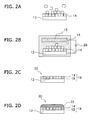
- FIG. 2A to FIG. 2C are figures showing a first aspect of a template layer preparation step in which FIG. 2A shows a grain layer formation process, FIG. 2B shows a fixing process, FIG. 2C shows a fixed grain body after the fixing process, and FIG. 2D shows a shaped body after a matrix formation process.
- FIG. 3A to FIG. 3C are figures showing a second aspect of the template layer preparation step in which FIG. 3A shows the grain layer formation process and the fixing process, FIG. 3B shows a re-polymerizing process, and FIG. 3C shows the fixed grain body.
- FIG. 4A to FIG. 4E are figures showing a third aspect of the template layer preparation step in which FIG. 4A shows an electrodeposition material formation process, FIG. 4B shows a drying process for the electrodeposition material 52, FIG. 4C shows a grain layer formation process, FIG. 4D shows a fixing process, and FIG. 4E shows a fixed grain body.
- the ceramic according to an embodiment is provided with a plurality of crystal grains that contain lead, lithium, and boron, are arranged in a planar direction, and have a mutually same crystal orientation with respect to the thickness direction (the direction that is vertical with respect to the planar direction).
- the ceramic according to the present aspect is a crystallographically -oriented ceramic, and more specifically, a plurality of crystal grains has the mutually same crystal orientation with respect to an in-plane thickness.
- the crystal grains are disposed in proximity through a grain boundary.
- the ceramic may include crystal grains having a different crystal orientation. More specifically, the proportion of crystal grains having the same crystal orientation in the ceramic is preferably 80 volume % or more, and more preferably 90 volume % or more.
- the ceramic may be described by the provision of a layer configured by crystal grains.
- a layer configured by crystal grains.
- a plurality of crystal grains are arranged in a planar direction, and one crystal grain is disposed in the thickness direction.
- the requirement for thin film formation is satisfied by at least a portion of the ceramic 1 having a single layer structure.
- the whole of the ceramic 1 has a single layer structure.
- the ceramic may be provided with two or more laminated layers with respect to the thickness direction of the ceramic. In other words, two or more crystal grains in the ceramic may be superimposed with respect to the thickness direction.
- the number of crystal grains in the thickness direction in the overall ceramic is uniform, the number of crystal grains in the thickness direction may vary at different positions within the ceramic.
- the ceramic may include titanium (Ti), zirconium (Zr), magnesium (Mg), niobium (Nb), nickel (Ni), sodium (Na), and/or barium (Ba).
- the ceramic may include as a principal component at least one substance selected from the group consisting of Pb(Zr, Ti)O 3 , Pb(Mg, Nb) (Zr, Ti)O 3 , Pb(Ni, Nb)(Zr, Ti)O 3 , Pb(Zn, Nb)(Zr, Ti)O 3 , Pb(Yb, Nb)(Zr, Ti)O 3 , (Pb, Sr)(Zr, Ti)O 3 , (Pb, Ba)(Zr, Ti)O 3 , (Pb, La)(Zr, Ti)O 3 , (Bi, Pb)(Ni, Nb)(Zr, Ti)O 3 , (Bi, Pb)(Mg, Nb)(Zr, Ti)O 3 , (Bi, Pb)(Zn, Nb)(Zr, Ti)O 3 , (Pb, Sr, La) (Mg, Ni, Nb)(Zr, Ti)O
- composition preferably comprises at least 70 wt.%, more preferably at least 80wt.%, and still more preferably at least 90wt.% of a specific substance.
- the presence of boron was can be confirmed using an electron probe microanalyser (EPMA).
- the presence of lithium can be confirmed using a chemical assay, a secondary ionization mass spectrometer (SIMS) or glow discharge optical emission spectroscopy (GD-OES).
- concentration of boron or lithium may vary in response to the initial concentration during manufacture or in a manufacturing step.
- a piezoelectric element according to an embodiment will be described making reference to FIG. 1 .
- a piezoelectric element 100 includes a piezoelectric body 101, and an upper electrode 102 and lower electrode 103 provided on both sides of the piezoelectric element 100.
- the ceramic described above in 1. is suitable for use as the piezoelectric body 101.
- a distortion is produced in the piezoelectric body 101 by a voltage applied from a power source (not shown) between the upper electrode 102 and the lower electrode 103 by electrically connecting the upper electrode 102 and the lower electrode 103 with the piezoelectric body 101.
- the piezoelectric body 101 can convert a pressure applied to the piezoelectric body 101 into a voltage.
- the piezoelectric element 100 may also be used as an electrostriction element. In other words, the ceramic above can be used as an electrostriction body.
- a known conductive material may be used as the upper electrode 102 and the lower electrode 103.
- the above ceramic can be sintered at a relatively low temperature, at least one of the following (1) or (2) can be applied to the upper electrode 102 and/or the lower electrode 103.
- the piezoelectric element 100 for example can be used in an apparatus such as an inkjet head, a speaker, a pressure sensor, or the like.
- FIG. 2 to FIG. 4 An aspect of a method of manufacturing the ceramic will be described referring to FIG. 2 to FIG. 4 .
- This method of manufacturing can be applied to the manufacture of the above ceramic.
- the object for manufacture by this method of manufacture is not limited to the above ceramic.
- the method includes the following steps (1) to (3).
- This step prepares the template layer in which the crystal orientation is arranged in a predetermined direction.
- the crystal orientation is arranged in a predetermined direction includes a state in which all the crystal orientation (for example (100) plane or the like) is arranged in a predetermined direction, a state in which a certain proportion, for example 60% or more, 80% or more of the total, of the crystal orientation is arranged in a predetermined direction, or the like.
- the template layer 19 includes a fixing compound that is fixed to a substrate 12 due to heat or a potential difference.
- the method of forming the template layer 19 includes the method shown in FIG. 2A to FIG.2C , and the method in FIG. 3A to FIG.3C , and FIG. 4A to FIG. 4D .
- a template layer 19 is prepared by fixing template grains 14 configured from a material containing lead onto a substrate 12. More specifically, the method includes a grain layer formation process, a fixing process, and a washing process.
- a layer configured by template grains 14 is formed on the substrate 12 in the grain layer formation process.
- the template grains 14 may be disposed on the surface of the substrate 12.
- the substrate 12 for example includes at least one of glass, a monocrystal, a ceramic, a resin and a metal.
- the glass substrate includes for example quartz and non-alkali glass.
- the monocrystal substrate includes for example silicon, gallium arsenide, silicon carbonate, alumina, and strontium titanate.
- the ceramic substrate includes for example stabilized zirconium oxide, aluminum oxide, magnesium oxide, mullite, aluminum nitride, and silicon nitride.
- the resin substrate includes an epoxy resin or a polyester resin.
- the metal substrate includes stainless steel, aluminum, or platinum. An insulation resin may be coated on the metal. In the following description, a substrate 12 formed from platinum will be described.
- the template grains 14 may be configured from a material containing lead.
- the template grains 14 for example may be prepared in advance to have a polyhedric shape.
- the template grains 14 are cubic in shape.
- the cubic crystals of the material containing lead for example can be prepared by a hydrothermal synthesis method.
- the material containing lead may use at least one substance selected from the group of substances given in (1) and (2) below.
- the size of the template grains 14 may have a size of 100 nm or more.
- the grain layer formation process arranges the template grains on the substrate.
- the grain layer formation process is a method that supplies a formed grain layer to the subsequent fixing process.
- the grain layer is formed without immersion of the substrate 12 in a solution.
- the grain layer is formed directly onto the substrate 12. This method of formation for example, may use one or more of a spray coating method, a spin-coat method, or a doctor blade method.
- the substrate 12 is immersed in a monomer solution 16 containing a chemical substance (monomer) that undergoes electropolymerization with a counter electrode 15 facing the substrate 12.
- the monomer undergoes electropolymerization on the substrate 12 due to the generation by the power source 28 of a potential difference between the substrate 12 and the counter electrode 15, and thereby forms a polymer.
- the polymer is shown as a resin 18 in the figure.
- the template layer 19 including the template grains 14 and the resin 18 is formed on the substrate 12.
- the resin 18 enters between the template grains 14 to thereby mechanically fix the template grains 14.
- the template grains 14 are fixed more strongly to the substrate 12 than a method of simply arranging the template grains 14 on the substrate 12.
- a fixed grain body 20 is obtained that includes a substrate 12 and a template layer 19.
- the monomer solution 16 is a solution that contains one or more monomers that polymerize as a result of electropolymerization and are dissolved in a solvent and/or dispersed in a dispersion medium.
- the monomer may be for example:
- the resin 18 after polymerization is the monomer polymer body described above. More specifically, the resin 18 includes polymer bodies of pyrrole-monomer such as pyrrole, alkylpyrrole, aminopyrrole, or the like, polymer bodies of aniline, or polymer bodies of thiofuran-monomer such as thiofuran, alkylthiofuran, thiofuran derivatives, or the like. In particular use of a pyrrole aqueous solution is preferred from among the solutions of the above monomers due to ease of handling.
- the monomer solution 16 may contain an oxidant such as an alkylbenzene sulfonate salt such as sodium p-toluenesulfonate, ethylbenzenesulfonic acid sodium, sodium dodecylbenzenesulfonate, or the like.
- an alkylbenzene sulfonate salt such as sodium p-toluenesulfonate, ethylbenzenesulfonic acid sodium, sodium dodecylbenzenesulfonate, or the like.
- the electrical conditions including voltage and current and the processing time for the electropolymerization may be varied in response to the size of the template grains to be fixed, and the thickness and size of the target grain layer.
- template grains 14 on the substrate 12 that is to say, template grains 14 that are not fixed by the resin 18 produced by electropolymerization are removed by a cleaning process.
- the cleaning process is performed by running water washing, ultrasonic cleaning, or the like.
- the grain layer may be formed by immersing the substrate 12 in a solution (slurry) containing the template grains 14.
- This type of method for example may include one, or a combination of two or more of the following methods:
- the slurry may include the above mentioned monomer that undergoes electric field polymerization.
- the grains When forming the grain layer, the grains may be disposed more densely on the substrate 12 by application of mechanical vibration, sound waves, heat, light or magnetic fields.
- a drying process and/or heating process may be performed after formation of the grain layer to thereby impart strength to the grain layer.
- FIG. 3A shows a method of sedimentation of the template grains 14 by immersion of the substrate 12 in the slurry. This method can be performed at the same time as the fixing process (electropolymerization of the fixing compound monomer), and even when performed after the fixing process, there is the advantage that transition of processing can be executed smoothly.
- the substrate 12 is immersed in a slurry 17 including the template grains 14 and the monomer that undergoes electropolymerization contained in a reaction vessel.
- a counter electrode 15 is disposed facing the substrate 12.
- the monomer After forming the grain layer on the substrate 12, the monomer undergoes electropolymerization as a result of continued immersion of the substrate 12 in the slurry 17. Consequently the template grains 14 are fixed to the substrate 12 by the polymerized resin 18. As a result, a template layer 19 is formed.
- the grain layer can also be formed on the substrate 12 by immersing and raising the substrate 12 in the slurry 17 in which the template grains 14 float in a membranous form on the surface of the liquid and the counter electrode 15 is opposed to the substrate 12 as shown in FIG. 3A .
- the monomer may undergo electropolymerization by creation of a potential difference between the substrate 12 and the counter electrode 15, and fix the grain layer with the polymerized resin 18.
- the formation of the grain layer and the fixing of the template grains 14 can be executed at substantially the same time. As a result, a relatively thin grain layer is obtained.
- the template layer preparation step may include a re-polymerization process. As shown in FIG. 3B , in the re-polymerization process, after passing through the grain layer formation process and the fixing process, the substrate 12 is immersed in the monomer solution 16 described above that contains monomers and does not contain template grains 14. The monomer can be subjected to electropolymerization on a subsequent occasion by providing a potential difference between substrate 12 and the counter electrode 15.
- the template layer 19 includes a further polymer body.
- elimination of template grains 14 from the uppermost layer is facilitated, and in other words, a template layer 19 is obtained in which the number of template grains 14 with respect to the thickness direction is one ( FIG. 3C ).
- a single layer of template grains 14 can be easily obtained by execution of a re-polymerization process ( FIG. 3B ) using a conductive monomer solution as the monomer solution 16.
- the cleaning process above may be performed after the re-polymerization process, or may be performed before and after the re-polymerization process.
- a fixed grain body 60 including a substrate 12 and template grains 14 fixed to the substrate 12 can be prepared by using a thermoplastic electrodeposition material as a fixing compound in the fixing process in substitution for a chemical substance that undergoes electropolymerization.
- This method includes an electrodeposition material layer formation process, a fixing process, and a cleaning process.
- the electrodeposition material layer formation process forms an electrodeposition material layer 52 that is configured as a layer of a thermoplastic electrodeposition material on the substrate 12.
- the substrate 12 is immersed in a thermoplastic electrodeposition material solution 51 that contains the thermoplastic electrodeposition material in a situation where the counter electrode 15 faces the substrate 12.
- the electrodeposition material layer 52 that is configured as a layer of a thermoplastic electrodeposition material is formed by producing a potential difference between the substrate 12 and the counter electrode 15 with the power source 29 ( FIG. 4B ).
- thermoplastic electrodeposition material may include for example:
- the solvent or the dispersion medium for the thermoplastic electrodeposition material solution 51 for example includes an inorganic solvent such as water or the like, or an organic solvent such as alcohol, or the like. More specifically, the thermoplastic electrodeposition material solution 51 may be a water-based electrodeposition coating material.
- the water-based electrodeposition coating material is preferably used due to simplicity of handling.
- the thermoplastic electrodeposition material solution 51 may include a catalyst such as a tin compound or a hardening agent such as a blocking isocyanate, or the like.
- the electrodeposition material layer 52 may be dried using a heater 54, or the like.
- the grain layer formation process disposes the template grains 14 on the electrodeposition material layer 52. Since the method of disposition of the template grains 14 has already been described, detailed description will not be repeated.
- the template grains 14 are fixed by the electrodeposition material layer 52 onto the substrate 12 by heating the electrodeposition material layer 52 to thereby form the template layer 59.
- the thermoplastic electrodeposition material in the electrodeposition material layer 52 is heated to a melting temperature by the heater 54.
- the heater 54 is disposed so that the substrate 12 is interposed between the heater 54 and the electrodeposition material layer 52.
- the fixing process may be executed by inserting the substrate 12 into an oven or the like and heating, or by irradiating electromagnetic waves onto the electrodeposition material layer 52.
- thermoplastic electrodeposition material enters between the template grains 14 as a result of the heating of the thermoplastic electrodeposition material, and thus mechanically fixes the template grains 14 in the template layer 59 onto the substrate 12 as a result of the thermoplastic electrodeposition material entering between the template grains 14.
- the cleaning process may also be executed in this aspect.
- the template layer preparation step according to the first to the third aspects includes a plurality of processes.
- the items described as processes or as elements of the different aspects may be mutually combined.
- the matrix formation step disposes a matrix material on the template layer.
- a matrix 22 is formed on the template layer 19 as shown in FIG. 2D .
- a shaped body 30 is prepared in this manner. All of the template layer preparation steps described above can be respectively combined with the matrix formation step or any subsequent step.
- the matrix material may be a mixture of an additive material including lithium or boron and a material containing lead.
- the additive material may be any material that adds lithium and boron to the matrix.
- the additive material that contains lithium and boron for example includes at least one compound selected from the group consisting of LiBO 2 , LiB 4 O 7 LiB(OH) 4 , Li 3 BO 3 , Li 6 B 4 O 9 LiB 3 O 5 , and Li 2 B 8 O 13 .
- lithium may be contained in at least one additive material of Li 2 CO 3 and LiF.
- the added amount of the additive material is preferably in the range of at least 0.05 wt.% to 10 wt.% or less of the overall matrix. When the added amount is 0.05 wt.% or more, a larger orientation effect is obtained. When the added amount is 10 wt.% or less, an effect is obtained that the residual amount after sintering is not excessive.
- the material containing lead may be a material described in relation to the material for the template grain.
- the material containing lead may be suitably selected in response to the composition or the like of the template grains 14 described above, or the target composition.
- the method of provision of the matrix material for example may include one, or a combination of two or more of the following methods:
- the sintering step sinters the resulting shaped body at a predetermined sintering temperature, removes the resin 18 and forms the template layer 19 and the matrix 22 into a piezoelectric body. In other words, this step forms a crystallographically -oriented ceramic.
- the sintering temperature is set in response to the composition of the target ceramic.
- the sintering temperature is set for example at 1100°C or less, and preferably to 1000°C or less.
- the sintering temperature is preferably set to 900°C or more.
- the temperature required for orientation of the crystals is suppressed to a lower temperature by the additive material including lithium and boron.
- the sintering atmosphere is not limited to a particular gas and may be an atmosphere of atmospheric air.
- the action of the additive material causes crystal growth in the matrix 22 in a crystal orientation that is arranged in a predetermined direction of the template layer 19.
- a ceramic can be manufactured with superior orientation in which the crystal orientation is arranged in a predetermined direction by sintering of the substrate 12 which forms the template layer 19 and the matrix 22 on a surface thereof.
- the reason that such an effect is obtained is conjectured to be due to the action of the additive material that includes lithium and boron in facilitating the growth of the material containing lead into a polyhedral shape.
- the lithium and boron content amount (concentration) in the sintered body may be lower than the shaped body before sintering.
- the method of manufacturing the ceramic may include a post-annealing step.
- the post-annealing step heats the sintered body (ceramic) obtained after the sintering step. In this step, the amount of the additive material contained in the ceramic is reduced.
- the post-annealing step for example may be executed under the same conditions of temperature, retaining time and atmospheric conditions as the conditions for the sintering step. Furthermore the post-annealing step for example may include one or a combination of the following methods:
- an electrically conductive material was used as the substrate 12.
- the substrate 12 can be used as an electrode in the fixing process.
- the template grains 14 can be directly disposed on the substrate 12.
- the substrate 12 can be used as a driving electrode for the piezoelectric body.
- a substrate 12 having surfaces with insulation characteristics may be used, an electrically conductive electrode may be disposed on the substrate 12, and the template grain 14 may be disposed on the electrode.
- the electrode that is used for fixing the template grains 14 can be used as a driving electrode for the piezoelectric body without further modification.
- the material used in the electrode for example may be at least one type selected from the group consisting of:
- a step in which template grains 14 are oriented on the substrate 12 in order to prepare template layer in which the crystal orientation is arranged in a predetermined direction has already been described as a template layer preparation step.
- the template layer preparation step may prepare a substrate in which the crystal orientation is arranged in a predetermined direction.
- the substrate itself functions as the template.
- a monocrystal substrate in which the crystal orientation is arranged in a predetermined direction may be used as the substrate in which the crystal orientation is arranged in a predetermined direction.
- the monocrystal substrate may be for example, silicon, gallium arsenide, silicon carbonate, alumina, and strontium titanate, magnesium oxide, calcium fluoride, lithium niobate, lithium tantalate, potassium tantalate, cerium oxide, and the like.
- a deposition film of platinum, titanium, strontium ruthenate, lanthanum nickelate, yttria stabilized zirconia, cerium oxide, and the like may be formed on the monocrystal substrate as a lower electrode or as a buffer layer that mitigates the lattice constant difference.
- the matrix may be directly formed on the surface of the substrate in the matrix formation step.
- a template sheet may be prepared by aligning the template grains 14 in which the crystal orientation is arranged in a predetermined direction, and forming into a sheet shape.
- a matrix sheet may be prepared by forming a mixed material that is a mixture of a material including lead and an additive material including lithium and boron into a sheet shape.
- a crystallographically-oriented ceramic may be manufactured by preparing a laminated body in which the template sheet and the matrix sheet are laminated alternately, and sintering the laminated body.
- a matrix laminated body may be manufactured by adhering these ceramic sheets together.
- the method of manufacture described above was a RGTT method (reactive template grain growth method). However as described above, there is no limitation on the method of manufacturing the ceramic.
- Platinum was plated with a thickness of 0.5 ⁇ m onto a 10 mm x 10mm zirconium base plate having a thickness of 0.5 mm, and used as a substrate.
- PZT lead zirconate titanate
- the grain diameter of the PZT grains is a median diameter (D50) measured using water as a dispersion medium with a dynamic scattering grain size distribution measuring apparatus Zetasizer Nano nano-ZS manufactured by Spectris Co., Ltd.
- the PZT grains were used as template grains in the following operation.
- Dodecylbenzenesulfonic acid sodium (Kanto Kagaku Co., Inc.) and pyrrole (Kanto Kagaku Co., Inc.) were added to 30 ml of pure water to have a concentration of 0.01 mol/L (liter) and thereby prepare a pyrrole aqueous solution.
- the pyrrole aqueous solution was placed in a beaker and 1 wt.% of the PZT grains was introduced into the pyrrole aqueous solution. Then a dispersing process was executed with a homogenizer to thereby prepare a turbid liquid (slurry).
- a SUS counter electrode was disposed with a 1-mm electrode interval to be parallel to the base plate and connected to a power source so that the base plate is the negative pole and the counter electrode is the positive pole.
- a polypyrrole was formed on the base plate by applying a 2 Hz triangular wave at a peak voltage of 5V on 30 occasions between the base plate and the counter electrode.
- the raw material for the matrix (hereafter termed the "piezoelectric body material") was lead oxide (Mitsui Mining and Smelting Co., Ltd.), titanium oxide (Ishihara Sangyo Kaisha, Ltd.), zirconium oxide (Nippon Denko Co., Ltd.), niobium oxide (Mitsui Mining and Smelting Co., Ltd.), bismuth oxide (Taiyo Koko Co., Ltd.), and nickel oxide (Seido Chemical Industry Co., Ltd.).
- An additive material such as lithium fluoride (LiF), or lithium carbonate (Li 2 CO 3 ) and lithium borate (LiBO 2 or Li 2 B 4 O 7 ) was added to 20BNN-80PZT in the concentration as shown in Table 1.
- LiF lithium fluoride
- Li 2 CO 3 lithium carbonate
- LiBO 2 or Li 2 B 4 O 7 lithium borate
- the concentration shown in Table 1 is a weight percent related to the overall matrix, that is to say, relative to the total of 20BNN-80PZT and the additive material.
- a powder was obtained by drying the mixed solution.
- a butyral binder (Sekisui Chemical Co., Ltd. BL-S), a dispersing agent (Kao Corporation SPO-30), a plasticizer (Kurogane Kasei Co., Ltd. DOP), and a dispersant (Katayama Chemical Ltd. terpineol) were added to the powder, to thereby obtain a PZT paste by kneading with a triroll mill.
- the PZT paste was coated uniformly by spin-coating on the base plate with PZT grains arranged thereon.
- the rotation speed for spin-coating was 1000 rpm and the coating period was 30 seconds.
- the base plate after coating was placed onto a hotplate and dried at 90°C for 5 minutes to thereby obtain a shaped body ( FIG. 2D ). This shaped body was subjected to degreasing for 2 hours at 500°C.
- the rate of temperature increase was 200°C/h, and the shaped body after degreasing was sintered at 1000°C for three hours.
- the atmosphere used during sintering was atmospheric air and after completion of sintering the rate of temperature decrease was 200°C/h.
- a ceramic sample was obtained by the above operation.
- X-ray diffraction was performed on the ceramic sample using an XRD apparatus (X-ray diffraction apparatus X'Pert MPD Pro, Spectris Co., Ltd.).
- the change in electrical resistance was measured by applying a 1 Hz triangular wave at 0 - 30V voltage in 1 billion pulses to the ceramic sample. Ceramics which had a change of less than 2% were determined to have a durability of "good".
- Dissipation loss in the sample in Example 1 and the comparative example 1 as described below were measured using an impedance analyzer. Ceramic samples having a dissipation loss of less than 10% were determined to be satisfactory.
- a sintered body was obtained using the same operational method described in example 1 with the exception that an additive material was not used.
- 20BNN-80PZT was obtained as a paste using the same procedure as the first example and was coated onto a Pt base plate having template grains arranged thereon using a spin-coating method. Thereafter, a ceramic sample was obtained after passing through degreasing and sintering (sintering temperature of 1200°C).
- a ceramic sample in Comparative Example 2 was prepared as described below using glass as an additive material.
- 20BNN-80PZT was obtained as a paste using the same procedure as the first example, glass was added as an additive material, and was coated onto a base plate having template grains arranged thereon using a spin-coating method. Thereafter, greasing was performed, and sintering was executed at a temperature of 1000°C. The conditions were the same as the first example with the exception that the additive material was different.
- Examples 1 - 21 had good durability, in Comparative Example 2, good durability was not obtained. Furthermore in Examples 1 - 21, although hetero-phase components were not identified, a hetero-phase component was observed in Comparative Example 2.
- Example 1 passed dissipative loss whereas Comparative Example 1 failed.
- [Table 1] Sample Added Agent Durability Hetero-phase Example 1 LiF 3% + Li 2 B 4 O 7 1% good no
- Example 2 LiF 3% + Li 2 B 4 O 7 3% good no
- Example 3 LiF 3% + Li 2 B 4 O 7 6% good no
- Example 4 LiF 6% + Li 2 B 4 O 7 1% good no
- Example 5 LiF 6% + Li 2 B 4 O 7 3% good no
- Example 6 LiF 6% + Li 2 B 4 O 7 6% good no
- Example 7 LiF 1% + Li 2 B 4 O 7 1% good no
- Example 8 LiF 1% + Li 2 B 4 O 7 3% good no
- Example 9 LiF 1% + Li 2 B 4 O 7 6% good no
- Example 10 Li 2 CO 3 1% + LiBO 2 0.1% good no
- Example 11 Li 2 CO 3 1% + LiBO 2 1% good no
- Example 12 Li 2 CO 3 1% + LiBO 2
Landscapes
- Engineering & Computer Science (AREA)
- Chemical & Material Sciences (AREA)
- Ceramic Engineering (AREA)
- Manufacturing & Machinery (AREA)
- Materials Engineering (AREA)
- Structural Engineering (AREA)
- Organic Chemistry (AREA)
- Inorganic Chemistry (AREA)
- Composite Materials (AREA)
- Compositions Of Oxide Ceramics (AREA)
Abstract
A ceramic having a plurality of crystal grains that contain lead, lithium, and boron, are arranged in a planar direction, and have a mutually same crystal orientation with respect to the thickness direction.
Description
- Technical Field
- The technical field relates to a new ceramic and a piezoelectric or electrostriction element using the ceramic.
- Description of the Related Art
- Patent Literature 1 (Japanese Patent Application Laid-Open No.
2001-261435 - Patent Literature 2 (European Patent Application Laid-Open No.
1972606 ) discloses the manufacture of a crystallographically-oriented ceramic using a PZT sheet having a preset orientation as a template. - Plate-like grains having a large aspect ratio and similar composition, such as Bi4Ti3O12 (termed BIT) in relation to the BNT-type piezoelectric body used in Patent Literature 1 cannot be obtained in a lead-based ceramic such as PZT or the like. Thus there are difficulties associated with obtaining a ceramic having high level of crystal orientation by application of an RTGG method to the structure of a lead-based ceramic.
- In recent years, in order to increase the field intensity, or in order to respond to the demand for downsizing of constitutive elements, there has been a demand to form the piezoelectric body as a thin layer and form the electrodes as a thin layer. However when there is a difference in the heat resistance between the electrodes and the piezoelectric body, and in particular when the electrodes have low resistance to heat, if the thin-layer electrodes and the piezoelectric body are sintered at the same time, there is the possibility that electrical conductivity will not be obtained due to the formation of a disconnection in the electrodes. Thus there is a need for a piezoelectric body that can be sintered at a lower temperature.
- The present invention is proposed in light of the outstanding problems above and has the object of providing a ceramic including lead that can be sintered at a low temperature.
- The ceramic according to a first aspect of the present invention is provided with a plurality of crystal grains that contain lead, lithium, and boron, are arranged in a planar direction (a first direction), and have the same crystal orientation with respect to the thickness direction (a second direction perpendicular to the first direction). The ceramic can be sintered at a relatively low temperature and therefore is preferably used in a small piezoelectric or electrostriction element.
- In at least a portion of the ceramic, the number of crystal grains disposed with respect to the thickness direction may be one.
- This ceramic may be used in a piezoelectric or electrostriction element including the ceramic and a pair of electrodes electrically connected with the ceramic. The thickness of the electrode may be less than or equal to 1 µm. The electrode may include silver or gold as a principal component, or may be a platinum or palladium plating film or sputtering film.
-
FIG. 1 is a sectional figure of a piezoelectric element according to an embodiment. -
FIG. 2A to FIG. 2C are figures showing a first aspect of a template layer preparation step in whichFIG. 2A shows a grain layer formation process,FIG. 2B shows a fixing process,FIG. 2C shows a fixed grain body after the fixing process, andFIG. 2D shows a shaped body after a matrix formation process. -
FIG. 3A to FIG. 3C are figures showing a second aspect of the template layer preparation step in whichFIG. 3A shows the grain layer formation process and the fixing process,FIG. 3B shows a re-polymerizing process, andFIG. 3C shows the fixed grain body. -
FIG. 4A to FIG. 4E are figures showing a third aspect of the template layer preparation step in whichFIG. 4A shows an electrodeposition material formation process,FIG. 4B shows a drying process for theelectrodeposition material 52,FIG. 4C shows a grain layer formation process,FIG. 4D shows a fixing process, andFIG. 4E shows a fixed grain body. - (1. Ceramic)
- The ceramic according to an embodiment is provided with a plurality of crystal grains that contain lead, lithium, and boron, are arranged in a planar direction, and have a mutually same crystal orientation with respect to the thickness direction (the direction that is vertical with respect to the planar direction). In other words, the ceramic according to the present aspect is a crystallographically -oriented ceramic, and more specifically, a plurality of crystal grains has the mutually same crystal orientation with respect to an in-plane thickness. The crystal grains are disposed in proximity through a grain boundary.
- However the ceramic may include crystal grains having a different crystal orientation. More specifically, the proportion of crystal grains having the same crystal orientation in the ceramic is preferably 80 volume % or more, and more preferably 90 volume % or more.
- The ceramic may be described by the provision of a layer configured by crystal grains. In a single layer, a plurality of crystal grains are arranged in a planar direction, and one crystal grain is disposed in the thickness direction. It is preferred that the requirement for thin film formation is satisfied by at least a portion of the ceramic 1 having a single layer structure. It is preferred that the whole of the ceramic 1 has a single layer structure. However the ceramic may be provided with two or more laminated layers with respect to the thickness direction of the ceramic. In other words, two or more crystal grains in the ceramic may be superimposed with respect to the thickness direction. Although it is preferred that the number of crystal grains in the thickness direction in the overall ceramic is uniform, the number of crystal grains in the thickness direction may vary at different positions within the ceramic.
- Various known materials for composing piezoelectric bodies, electrostriction bodies, or crystallographically-oriented ceramics may be used as the material configuring the ceramic. More specifically, in addition to lead, the ceramic may include titanium (Ti), zirconium (Zr), magnesium (Mg), niobium (Nb), nickel (Ni), sodium (Na), and/or barium (Ba). More specifically, the ceramic may include as a principal component at least one substance selected from the group consisting of Pb(Zr, Ti)O3, Pb(Mg, Nb) (Zr, Ti)O3, Pb(Ni, Nb)(Zr, Ti)O3, Pb(Zn, Nb)(Zr, Ti)O3, Pb(Yb, Nb)(Zr, Ti)O3, (Pb, Sr)(Zr, Ti)O3, (Pb, Ba)(Zr, Ti)O3, (Pb, La)(Zr, Ti)O3, (Bi, Pb)(Ni, Nb)(Zr, Ti)O3, (Bi, Pb)(Mg, Nb)(Zr, Ti)O3, (Bi, Pb)(Zn, Nb)(Zr, Ti)O3, (Pb, Sr, La) (Mg, Ni, Nb)(Zr, Ti)O3, PbTiO3, Pb(Mg, Nb)TiO3, Pb(Ni, Nb)TiO3, and Pb(Zn, Nb)TiO3.
- In the present specification, "includes as a principal component" means that a certain composition preferably comprises at least 70 wt.%, more preferably at least 80wt.%, and still more preferably at least 90wt.% of a specific substance.
- The presence of boron was can be confirmed using an electron probe microanalyser (EPMA). The presence of lithium can be confirmed using a chemical assay, a secondary ionization mass spectrometer (SIMS) or glow discharge optical emission spectroscopy (GD-OES). There is no particular limitation on the concentration of boron or lithium, and such concentration may vary in response to the initial concentration during manufacture or in a manufacturing step.
- (2. Piezoelectric Element)
- A piezoelectric element according to an embodiment will be described making reference to
FIG. 1 . - As shown in
FIG. 1 , apiezoelectric element 100 includes apiezoelectric body 101, and anupper electrode 102 andlower electrode 103 provided on both sides of thepiezoelectric element 100. The ceramic described above in 1. is suitable for use as thepiezoelectric body 101. A distortion is produced in thepiezoelectric body 101 by a voltage applied from a power source (not shown) between theupper electrode 102 and thelower electrode 103 by electrically connecting theupper electrode 102 and thelower electrode 103 with thepiezoelectric body 101. Thepiezoelectric body 101 can convert a pressure applied to thepiezoelectric body 101 into a voltage. Thepiezoelectric element 100 may also be used as an electrostriction element. In other words, the ceramic above can be used as an electrostriction body. - A known conductive material may be used as the
upper electrode 102 and thelower electrode 103. In particular, since the above ceramic can be sintered at a relatively low temperature, at least one of the following (1) or (2) can be applied to theupper electrode 102 and/or thelower electrode 103. - (1) use of a material having low heat resistance as the principal component;
- (2) reduction of the film thickness of the electrode (for example a thickness of 1 µm or less).
- The
piezoelectric element 100 for example can be used in an apparatus such as an inkjet head, a speaker, a pressure sensor, or the like. - (3. Method of Manufacturing Ceramic)
- An aspect of a method of manufacturing the ceramic will be described referring to
FIG. 2 to FIG. 4 . This method of manufacturing can be applied to the manufacture of the above ceramic. However there is no limitation on the method of manufacturing the above ceramic, and the object for manufacture by this method of manufacture is not limited to the above ceramic. - The method includes the following steps (1) to (3).
- (1) A template layer preparation step for preparing a template layer in which the crystal orientation is arranged in a predetermined direction;
- (2) A matrix formation step in which a matrix is formed by disposing a mixed material on the template layer, the mixed material being a mixture of a material including lead and an additive material including lithium and boron; and
- (3) A sintering step in which the matrix and the template layer are sintered at a predetermined sintering temperature.
- (1) Template Layer Preparation Step
- This step prepares the template layer in which the crystal orientation is arranged in a predetermined direction. "The crystal orientation is arranged in a predetermined direction" includes a state in which all the crystal orientation (for example (100) plane or the like) is arranged in a predetermined direction, a state in which a certain proportion, for example 60% or more, 80% or more of the total, of the crystal orientation is arranged in a predetermined direction, or the like.
- The
template layer 19 includes a fixing compound that is fixed to asubstrate 12 due to heat or a potential difference. The method of forming thetemplate layer 19 includes the method shown inFIG. 2A to FIG.2C , and the method inFIG. 3A to FIG.3C , andFIG. 4A to FIG. 4D . - (1-1) First Aspect of Template Preparation Layer Step
- A first aspect of the template preparation layer step will be described making reference to
FIG. 2A to FIG. 2C . In the present aspect, atemplate layer 19 is prepared by fixingtemplate grains 14 configured from a material containing lead onto asubstrate 12. More specifically, the method includes a grain layer formation process, a fixing process, and a washing process. - As shown in
FIG. 2A , a layer configured bytemplate grains 14 is formed on thesubstrate 12 in the grain layer formation process. - The
template grains 14 may be disposed on the surface of thesubstrate 12. Thesubstrate 12 for example includes at least one of glass, a monocrystal, a ceramic, a resin and a metal. The glass substrate includes for example quartz and non-alkali glass. The monocrystal substrate includes for example silicon, gallium arsenide, silicon carbonate, alumina, and strontium titanate. The ceramic substrate includes for example stabilized zirconium oxide, aluminum oxide, magnesium oxide, mullite, aluminum nitride, and silicon nitride. The resin substrate includes an epoxy resin or a polyester resin. The metal substrate includes stainless steel, aluminum, or platinum. An insulation resin may be coated on the metal. In the following description, asubstrate 12 formed from platinum will be described. - The
template grains 14 may be configured from a material containing lead. Thetemplate grains 14 for example may be prepared in advance to have a polyhedric shape. Preferably, thetemplate grains 14 are cubic in shape. The cubic crystals of the material containing lead for example can be prepared by a hydrothermal synthesis method. For example, the material containing lead may use at least one substance selected from the group of substances given in (1) and (2) below. - (1) Pb(Zr, Ti)O3, Pb(Mg, Nb) (Zr, Ti)O3, Pb(Ni, Nb)(Zr, Ti)O3, Pb(Zn, Nb)(Zr, Ti)O3, Pb(Yb, Nb)(Zr, Ti)O3, (Pb, Sr)(Zr, Ti)O3, (Pb, Ba)(Zr, Ti)O3, (Pb, La)(Zr, Ti)O3, (Bi, Pb)(Ni, Nb)(Zr, Ti)O3, (Bi, Pb)(Mg, Nb)(Zr, Ti)O3, (Bi, Pb)(Zn, Nb)(Zr, Ti)O3, (Pb, Sr, La) (Mg, Ni, Nb)(Zr, Ti)O3, PbTiO3, Pb(Mg, Nb)TiO3, Pb(Ni, Nb)TiO3, and Pb(Zn, Nb)TiO3.
- (2) A raw material formed from the above compositions after sintering (for example, the hydroxides, the oxides or the like of these substances).
- Although there is no particular limitation on the size of the
template grains 14 with reference to a specific value, the grains for example may have a size of 100 nm or more. - (Grain Layer Formation Process)
- The grain layer formation process arranges the template grains on the substrate. There is no particular limitation on the specific details of the grain layer formation process as long as it is a method that supplies a formed grain layer to the subsequent fixing process. For example, as shown in
FIG. 2A , the grain layer is formed without immersion of thesubstrate 12 in a solution. Furthermore inFIG. 2A , the grain layer is formed directly onto thesubstrate 12. This method of formation for example, may use one or more of a spray coating method, a spin-coat method, or a doctor blade method. - (Fixing Process)
- As shown in
FIG. 2B , in the fixing process, thesubstrate 12 is immersed in amonomer solution 16 containing a chemical substance (monomer) that undergoes electropolymerization with acounter electrode 15 facing thesubstrate 12. The monomer undergoes electropolymerization on thesubstrate 12 due to the generation by thepower source 28 of a potential difference between thesubstrate 12 and thecounter electrode 15, and thereby forms a polymer. The polymer is shown as aresin 18 in the figure. - In this manner, as shown in
FIG. 2C , thetemplate layer 19 including thetemplate grains 14 and theresin 18 is formed on thesubstrate 12. Theresin 18 enters between thetemplate grains 14 to thereby mechanically fix thetemplate grains 14. Thus thetemplate grains 14 are fixed more strongly to thesubstrate 12 than a method of simply arranging thetemplate grains 14 on thesubstrate 12. In this manner, a fixedgrain body 20 is obtained that includes asubstrate 12 and atemplate layer 19. - The
monomer solution 16 is a solution that contains one or more monomers that polymerize as a result of electropolymerization and are dissolved in a solvent and/or dispersed in a dispersion medium. - The monomer may be for example:
- a type of vinyl monomer such as styrene, N-vinylcarbazole, or the like;
- an aromatic compound such as aniline, phenol, or the like; and
- a heterocyclic compound such as pyrrole, thiofuran, furan, or the like.
- a polymerization reaction mediated by radical cations or radical anions;
- a polymerization reaction caused by reactive species such reduced cations, anions and free radicals generated by oxidation or reduction of coexisting supporting electrolyte or added agents;
- chain polymerization; and
- step-growth polymerization.
- The
resin 18 after polymerization is the monomer polymer body described above. More specifically, theresin 18 includes polymer bodies of pyrrole-monomer such as pyrrole, alkylpyrrole, aminopyrrole, or the like, polymer bodies of aniline, or polymer bodies of thiofuran-monomer such as thiofuran, alkylthiofuran, thiofuran derivatives, or the like.
In particular use of a pyrrole aqueous solution is preferred from among the solutions of the above monomers due to ease of handling. - In order to induce electropolymerization, the
monomer solution 16 may contain an oxidant such as an alkylbenzene sulfonate salt such as sodium p-toluenesulfonate, ethylbenzenesulfonic acid sodium, sodium dodecylbenzenesulfonate, or the like. - The electrical conditions including voltage and current and the processing time for the electropolymerization may be varied in response to the size of the template grains to be fixed, and the thickness and size of the target grain layer.
- (Cleaning Process)
-
Excess template grains 14 on thesubstrate 12, that is to say,template grains 14 that are not fixed by theresin 18 produced by electropolymerization are removed by a cleaning process. The cleaning process is performed by running water washing, ultrasonic cleaning, or the like. - (1-2) Second Aspect of the Template Layer Preparation Step
- Description which overlaps with the first aspect will not be repeated in the following description. In other words, materials and processing that are not described below adopt a configuration that is the same as the first aspect.
- (Grain Layer Formation Process and Fixing Process)
- The grain layer may be formed by immersing the
substrate 12 in a solution (slurry) containing thetemplate grains 14. This type of method for example may include one, or a combination of two or more of the following methods: - a method of sedimentation of the
template grains 14 in the slurry by immersing and holding stationary thesubstrate 12 in the slurry that contains a dispersal of thetemplate grains 14; - an LB method in which the
template grains 14 are arranged in a liquid phase interface, and the substrate that is immersed in a lower phase is raised; - a method of electrophoresis; and
- a dipping method.
- The slurry may include the above mentioned monomer that undergoes electric field polymerization.
- When forming the grain layer, the grains may be disposed more densely on the
substrate 12 by application of mechanical vibration, sound waves, heat, light or magnetic fields. - Since the grain layer is immersed in a solution in the fixing process, a drying process and/or heating process may be performed after formation of the grain layer to thereby impart strength to the grain layer. [0041]
-
FIG. 3A shows a method of sedimentation of thetemplate grains 14 by immersion of thesubstrate 12 in the slurry. This method can be performed at the same time as the fixing process (electropolymerization of the fixing compound monomer), and even when performed after the fixing process, there is the advantage that transition of processing can be executed smoothly. - As shown in
FIG. 3A , thesubstrate 12 is immersed in aslurry 17 including thetemplate grains 14 and the monomer that undergoes electropolymerization contained in a reaction vessel. In the reaction vessel, acounter electrode 15 is disposed facing thesubstrate 12. - After forming the grain layer on the
substrate 12, the monomer undergoes electropolymerization as a result of continued immersion of thesubstrate 12 in theslurry 17. Consequently thetemplate grains 14 are fixed to thesubstrate 12 by the polymerizedresin 18. As a result, atemplate layer 19 is formed. - The grain layer can also be formed on the
substrate 12 by immersing and raising thesubstrate 12 in theslurry 17 in which thetemplate grains 14 float in a membranous form on the surface of the liquid and thecounter electrode 15 is opposed to thesubstrate 12 as shown inFIG. 3A . In this case, when thesubstrate 12 is raised, the monomer may undergo electropolymerization by creation of a potential difference between thesubstrate 12 and thecounter electrode 15, and fix the grain layer with the polymerizedresin 18. According to this process, the formation of the grain layer and the fixing of thetemplate grains 14 can be executed at substantially the same time. As a result, a relatively thin grain layer is obtained. - The template layer preparation step may include a re-polymerization process. As shown in
FIG. 3B , in the re-polymerization process, after passing through the grain layer formation process and the fixing process, thesubstrate 12 is immersed in themonomer solution 16 described above that contains monomers and does not containtemplate grains 14. The monomer can be subjected to electropolymerization on a subsequent occasion by providing a potential difference betweensubstrate 12 and thecounter electrode 15. - After passing through this process, the
template layer 19 includes a further polymer body. As a result, elimination oftemplate grains 14 from the uppermost layer is facilitated, and in other words, atemplate layer 19 is obtained in which the number oftemplate grains 14 with respect to the thickness direction is one (FIG. 3C ). - For example, in the fixing process (
FIG. 3A ), when template grains from a sub-micron size to several microns are fixed by a conductive polymer, a single layer oftemplate grains 14 can be easily obtained by execution of a re-polymerization process (FIG. 3B ) using a conductive monomer solution as themonomer solution 16. - The cleaning process above may be performed after the re-polymerization process, or may be performed before and after the re-polymerization process.
- (1-3) Third Aspect of the Template Layer Preparation Step
- Description which overlaps with the first aspect or the second aspect will not be repeated in the following description. In other words, materials and processing that are not described below adopts a configuration that is the same as the first aspect or the second aspect.
- According to the methods shown in
FIG. 4A to FIG. 4E , a fixedgrain body 60 including asubstrate 12 andtemplate grains 14 fixed to thesubstrate 12 can be prepared by using a thermoplastic electrodeposition material as a fixing compound in the fixing process in substitution for a chemical substance that undergoes electropolymerization. This method includes an electrodeposition material layer formation process, a fixing process, and a cleaning process. - (Electrodeposition Material Layer Formation Process)
- As shown in
FIG. 4A , the electrodeposition material layer formation process forms anelectrodeposition material layer 52 that is configured as a layer of a thermoplastic electrodeposition material on thesubstrate 12. In the electrodeposition material layer formation process, thesubstrate 12 is immersed in a thermoplasticelectrodeposition material solution 51 that contains the thermoplastic electrodeposition material in a situation where thecounter electrode 15 faces thesubstrate 12. Theelectrodeposition material layer 52 that is configured as a layer of a thermoplastic electrodeposition material is formed by producing a potential difference between thesubstrate 12 and thecounter electrode 15 with the power source 29 (FIG. 4B ). - The thermoplastic electrodeposition material may include for example:
- a carbon-based polymer compound such as an epoxy resin, a polyimide resin, a polyamide-imide resin, and acrylic resin, or the like;
- a silicon-based polymer compound such as a silicon resin, or the like; and
- an oxide nanograin of alumina for example that has a dispersant adhered to a surface thereof and that has an electrostatic charge.
- The solvent or the dispersion medium for the thermoplastic
electrodeposition material solution 51 for example includes an inorganic solvent such as water or the like, or an organic solvent such as alcohol, or the like. More specifically, the thermoplasticelectrodeposition material solution 51 may be a water-based electrodeposition coating material. The water-based electrodeposition coating material is preferably used due to simplicity of handling. - The thermoplastic
electrodeposition material solution 51 may include a catalyst such as a tin compound or a hardening agent such as a blocking isocyanate, or the like. - As shown in
FIG. 4B , theelectrodeposition material layer 52 may be dried using aheater 54, or the like. - As shown in
FIG. 4C , the grain layer formation process disposes thetemplate grains 14 on theelectrodeposition material layer 52. Since the method of disposition of thetemplate grains 14 has already been described, detailed description will not be repeated. - Next, the
template grains 14 are fixed by theelectrodeposition material layer 52 onto thesubstrate 12 by heating theelectrodeposition material layer 52 to thereby form the template layer 59. InFIG. 4D , the thermoplastic electrodeposition material in theelectrodeposition material layer 52 is heated to a melting temperature by theheater 54. InFIG. 4D , theheater 54 is disposed so that thesubstrate 12 is interposed between theheater 54 and theelectrodeposition material layer 52. - The fixing process may be executed by inserting the
substrate 12 into an oven or the like and heating, or by irradiating electromagnetic waves onto theelectrodeposition material layer 52. - The thermoplastic electrodeposition material enters between the
template grains 14 as a result of the heating of the thermoplastic electrodeposition material, and thus mechanically fixes thetemplate grains 14 in the template layer 59 onto thesubstrate 12 as a result of the thermoplastic electrodeposition material entering between thetemplate grains 14. - Needless to say, the cleaning process may also be executed in this aspect.
- As described above, the template layer preparation step according to the first to the third aspects includes a plurality of processes. The items described as processes or as elements of the different aspects may be mutually combined.
- (2) Matrix Formation Step
- The matrix formation step disposes a matrix material on the template layer. In this manner, for example, in the fixed
grain body 20 as shown inFIG. 2C , amatrix 22 is formed on thetemplate layer 19 as shown inFIG. 2D . A shapedbody 30 is prepared in this manner. All of the template layer preparation steps described above can be respectively combined with the matrix formation step or any subsequent step. - The matrix material may be a mixture of an additive material including lithium or boron and a material containing lead.
- There is no particular limitation on the additive material to a specific composition and it may be any material that adds lithium and boron to the matrix. The additive material that contains lithium and boron for example includes at least one compound selected from the group consisting of LiBO2, LiB4O7 LiB(OH)4, Li3BO3, Li6B4O9 LiB3O5, and Li2B8O13. Furthermore lithium may be contained in at least one additive material of Li2CO3 and LiF.
- The added amount of the additive material is preferably in the range of at least 0.05 wt.% to 10 wt.% or less of the overall matrix. When the added amount is 0.05 wt.% or more, a larger orientation effect is obtained. When the added amount is 10 wt.% or less, an effect is obtained that the residual amount after sintering is not excessive.
- The material containing lead may be a material described in relation to the material for the template grain. The material containing lead may be suitably selected in response to the composition or the like of the
template grains 14 described above, or the target composition. - The method of provision of the matrix material for example may include one, or a combination of two or more of the following methods:
- a method of coating by spraying;
- a method of spin-coating;
- a doctor-blade method; and
- a dipping method.
- The sintering step sinters the resulting shaped body at a predetermined sintering temperature, removes the
resin 18 and forms thetemplate layer 19 and thematrix 22 into a piezoelectric body. In other words, this step forms a crystallographically -oriented ceramic. - The sintering temperature is set in response to the composition of the target ceramic. The sintering temperature is set for example at 1100°C or less, and preferably to 1000°C or less. The sintering temperature is preferably set to 900°C or more. The temperature required for orientation of the crystals is suppressed to a lower temperature by the additive material including lithium and boron.
- The sintering atmosphere is not limited to a particular gas and may be an atmosphere of atmospheric air.
- During the sintering step, the action of the additive material causes crystal growth in the
matrix 22 in a crystal orientation that is arranged in a predetermined direction of thetemplate layer 19. Thus a ceramic can be manufactured with superior orientation in which the crystal orientation is arranged in a predetermined direction by sintering of thesubstrate 12 which forms thetemplate layer 19 and thematrix 22 on a surface thereof. The reason that such an effect is obtained is conjectured to be due to the action of the additive material that includes lithium and boron in facilitating the growth of the material containing lead into a polyhedral shape. - Since lithium and boron are vaporized by sintering, the lithium and boron content amount (concentration) in the sintered body may be lower than the shaped body before sintering.
- The method of manufacturing the ceramic may include a post-annealing step. The post-annealing step heats the sintered body (ceramic) obtained after the sintering step. In this step, the amount of the additive material contained in the ceramic is reduced.
- The post-annealing step for example may be executed under the same conditions of temperature, retaining time and atmospheric conditions as the conditions for the sintering step. Furthermore the post-annealing step for example may include one or a combination of the following methods:
- long-term retention at a temperature lower than the conditions for the sintering step, for example a temperature of at least 700°C and 1000 °C or less; or
- heating in an atmosphere in which the partial pressure of oxygen adjusted to a pressure in which the additive material tends to vaporize.
- The present invention is not limited to the aspects described above, and various modifications may be added within a scope that does not depart from the spirit of the present invention. For example, the above aspects may be modified in the following manner.
- In the above aspects, an electrically conductive material was used as the
substrate 12. Thus thesubstrate 12 can be used as an electrode in the fixing process. For that reason, thetemplate grains 14 can be directly disposed on thesubstrate 12. Furthermore thesubstrate 12 can be used as a driving electrode for the piezoelectric body. - A
substrate 12 having surfaces with insulation characteristics may be used, an electrically conductive electrode may be disposed on thesubstrate 12, and thetemplate grain 14 may be disposed on the electrode. In this manner, the electrode that is used for fixing thetemplate grains 14 can be used as a driving electrode for the piezoelectric body without further modification. The material used in the electrode for example may be at least one type selected from the group consisting of: - platinum, palladium, ruthenium, gold, and silver;
- alloys thereof; and
- conductive polymers.
- A step in which
template grains 14 are oriented on thesubstrate 12 in order to prepare template layer in which the crystal orientation is arranged in a predetermined direction has already been described as a template layer preparation step. - In addition, the template layer preparation step may prepare a substrate in which the crystal orientation is arranged in a predetermined direction. When using this substrate, there is no need to provide template grains on the substrate. In other words, the substrate itself functions as the template.
- A monocrystal substrate in which the crystal orientation is arranged in a predetermined direction may be used as the substrate in which the crystal orientation is arranged in a predetermined direction. The monocrystal substrate may be for example, silicon, gallium arsenide, silicon carbonate, alumina, and strontium titanate, magnesium oxide, calcium fluoride, lithium niobate, lithium tantalate, potassium tantalate, cerium oxide, and the like.
- A deposition film of platinum, titanium, strontium ruthenate, lanthanum nickelate, yttria stabilized zirconia, cerium oxide, and the like may be formed on the monocrystal substrate as a lower electrode or as a buffer layer that mitigates the lattice constant difference.
- In this manner, when the substrate itself acts as a template, the matrix may be directly formed on the surface of the substrate in the matrix formation step.
- Furthermore at least one of the template layer and the matrix may be pre-formed as a sheet. For example, a template sheet may be prepared by aligning the
template grains 14 in which the crystal orientation is arranged in a predetermined direction, and forming into a sheet shape. A matrix sheet may be prepared by forming a mixed material that is a mixture of a material including lead and an additive material including lithium and boron into a sheet shape. A crystallographically-oriented ceramic may be manufactured by preparing a laminated body in which the template sheet and the matrix sheet are laminated alternately, and sintering the laminated body. - After preparing ceramic sheets by sintering the template layer and the matrix together, a matrix laminated body may be manufactured by adhering these ceramic sheets together.
- The method of manufacture described above was a RGTT method (reactive template grain growth method). However as described above, there is no limitation on the method of manufacturing the ceramic.
- While only selected embodiments have been chosen to illustrate the present invention, it will be apparent to those skilled in the art from this disclosure that various changes and modifications can be made herein without departing from the scope of the invention as defined in the appended claims. Furthermore, the foregoing descriptions of the embodiments according to the present invention are provided for illustration only, and not for the purpose of limiting the invention as defined by the appended claims and their equivalents. Thus, the scope of the invention is not limited to the disclosed embodiments.
- [Examples]
- Examples of the present invention will be described in detail below. However these examples do not limit the invention.
- Platinum was plated with a thickness of 0.5 µm onto a 10 mm x 10mm zirconium base plate having a thickness of 0.5 mm, and used as a substrate.
- The raw material for the template layer uses a lead aqueous solution including lead acetate trihydrate (Kanto Kagaku Co., Inc.), ethylenediaminetetraacetic acid (Kanto Kagaku Co., Inc.), and potassium hydroxide (Kanto Kagaku Co., Inc.); an aqueous solution of zirconium containing zirconyl chloride octahydrate (Kanto Kagaku Co., Inc.); an aqueous solution of titanium chloride (Wako Pure Chemical Industries, Ltd.); and an aqueous solution of potassium hydroxide containing potassium hydroxide (Kanto Kagaku Co., Inc.). These raw materials were mixed in a molar ratio (ratio of numbers of atoms) of Pb:Zr:Ti = 1.1:0.7:0.3 to prepare a raw material solution.
- 30 ml of the raw material solution was placed into a 100 ml SUS pressure vessel having inner walls of polytetrafluoro-ethylene, and subjected to hydrothermal synthesis for 4 hours at 165°C to obtain lead zirconate titanate (hereafter PZT) grains having a cubic shape and a grain diameter of 2 µm. The grain diameter of the PZT grains is a median diameter (D50) measured using water as a dispersion medium with a dynamic scattering grain size distribution measuring apparatus Zetasizer Nano nano-ZS manufactured by Spectris Co., Ltd. The PZT grains were used as template grains in the following operation.
- ii) Formation of Template Layer
- Dodecylbenzenesulfonic acid sodium (Kanto Kagaku Co., Inc.) and pyrrole (Kanto Kagaku Co., Inc.) were added to 30 ml of pure water to have a concentration of 0.01 mol/L (liter) and thereby prepare a pyrrole aqueous solution. The pyrrole aqueous solution was placed in a beaker and 1 wt.% of the PZT grains was introduced into the pyrrole aqueous solution. Then a dispersing process was executed with a homogenizer to thereby prepare a turbid liquid (slurry).
- Then the above base plate was placed on the bottom of the beaker holding the slurry, and held in a stationary position for 10 minutes until the PZT grains sediment and build up thereon.
- Next, a SUS counter electrode was disposed with a 1-mm electrode interval to be parallel to the base plate and connected to a power source so that the base plate is the negative pole and the counter electrode is the positive pole. A polypyrrole was formed on the base plate by applying a 2 Hz triangular wave at a peak voltage of 5V on 30 occasions between the base plate and the counter electrode.
- Excess PZT grains were removed by rocking the base plate having the polypyrrole deposition film in the aqueous solution. Thereafter ultrasonic cleaning in pure water was executed to thereby remove PZT grains attached to portions other than the base plate. The ultrasonic cleaning was performed under conditions of 40 kHz and 1 minute using an ultrasonic cleaning apparatus (UT-106, Sharp Corporation).
- The operation above obtained a base plate in which the planar direction of the PZT grains was fixed in a membranous direction on a platinum base plate arranged in a (100) direction.
- 1-2 Matrix Formation Step, Sintering Step
- The raw material for the matrix (hereafter termed the "piezoelectric body material") was lead oxide (Mitsui Mining and Smelting Co., Ltd.), titanium oxide (Ishihara Sangyo Kaisha, Ltd.), zirconium oxide (Nippon Denko Co., Ltd.), niobium oxide (Mitsui Mining and Smelting Co., Ltd.), bismuth oxide (Taiyo Koko Co., Ltd.), and nickel oxide (Seido Chemical Industry Co., Ltd.). These raw materials were used in a known solid phase reaction method to prepare a composition of nickel bismuth niobate (Bi(Ni, Nb) O3) and lead zirconate titanate (Pb(Zr, Ti) O3) having a composition ratio of 2:8 (hereafter termed "20BNN-80PZT").
- An additive material such as lithium fluoride (LiF), or lithium carbonate (Li2CO3) and lithium borate (LiBO2 or Li2B4O7) was added to 20BNN-80PZT in the concentration as shown in Table 1. Using acetone as a solvent, 20BNN-80PZT and the additive material were mixed for 24 hours in a polyethylene vessel.
The concentration shown in Table 1 is a weight percent related to the overall matrix, that is to say, relative to the total of 20BNN-80PZT and the additive material. - A powder was obtained by drying the mixed solution. A butyral binder (Sekisui Chemical Co., Ltd. BL-S), a dispersing agent (Kao Corporation SPO-30), a plasticizer (Kurogane Kasei Co., Ltd. DOP), and a dispersant (Katayama Chemical Ltd. terpineol) were added to the powder, to thereby obtain a PZT paste by kneading with a triroll mill.
- The PZT paste was coated uniformly by spin-coating on the base plate with PZT grains arranged thereon. The rotation speed for spin-coating was 1000 rpm and the coating period was 30 seconds. The base plate after coating was placed onto a hotplate and dried at 90°C for 5 minutes to thereby obtain a shaped body (
FIG. 2D ). This shaped body was subjected to degreasing for 2 hours at 500°C. - The rate of temperature increase was 200°C/h, and the shaped body after degreasing was sintered at 1000°C for three hours. The atmosphere used during sintering was atmospheric air and after completion of sintering the rate of temperature decrease was 200°C/h.
A ceramic sample was obtained by the above operation. - The presence of boron was confirmed using an electron probe micro-analyzer (EPMA).
Furthermore the presence of lithium in the sintered body was confirmed by dissolving the ceramic sample in acid and subjecting to inductively coupled plasma (ICP) emission spectrographic analysis. - X-ray diffraction (XRD) was performed on the ceramic sample using an XRD apparatus (X-ray diffraction apparatus X'Pert MPD Pro, Spectris Co., Ltd.).
- The change in electrical resistance was measured by applying a 1 Hz triangular wave at 0 - 30V voltage in 1 billion pulses to the ceramic sample. Ceramics which had a change of less than 2% were determined to have a durability of "good".
- Dissipation loss in the sample in Example 1 and the comparative example 1 as described below were measured using an impedance analyzer. Ceramic samples having a dissipation loss of less than 10% were determined to be satisfactory.
- A sintered body was obtained using the same operational method described in example 1 with the exception that an additive material was not used. In other words, 20BNN-80PZT was obtained as a paste using the same procedure as the first example and was coated onto a Pt base plate having template grains arranged thereon using a spin-coating method. Thereafter, a ceramic sample was obtained after passing through degreasing and sintering (sintering temperature of 1200°C).
- A ceramic sample in Comparative Example 2 was prepared as described below using glass as an additive material. 20BNN-80PZT was obtained as a paste using the same procedure as the first example, glass was added as an additive material, and was coated onto a base plate having template grains arranged thereon using a spin-coating method. Thereafter, greasing was performed, and sintering was executed at a temperature of 1000°C. The conditions were the same as the first example with the exception that the additive material was different.
- Results
- The presence of lithium and boron was confirmed in the ceramic sample in Examples 1 - 21.
- The results of XRD did not identify hetero-phase components in any of the Examples 1 - 21 (Table 1).
- Although Examples 1 - 21 had good durability, in Comparative Example 2, good durability was not obtained. Furthermore in Examples 1 - 21, although hetero-phase components were not identified, a hetero-phase component was observed in Comparative Example 2.
- Example 1 passed dissipative loss whereas Comparative Example 1 failed.
[Table 1] Sample Added Agent Durability Hetero-phase Example 1 LiF 3% + Li2B4O7 1% good no Example 2 LiF 3% + Li2B4O7 3% good no Example 3 LiF 3% + Li2B4O7 6% good no Example 4 LiF 6% + Li2B4O7 1% good no Example 5 LiF 6% + Li2B4O7 3% good no Example 6 LiF 6% + Li2B4O7 6% good no Example 7 LiF 1% + Li2B4O7 1% good no Example 8 LiF 1% + Li2B4O7 3% good no Example 9 LiF 1% + Li2B4O7 6% good no Example 10 Li2CO3 1% + LiBO2 0.1% good no Example 11 Li2CO3 1% + LiBO2 1% good no Example 12 Li2CO3 1% + LiBO2 3% good no Example 13 Li2CO3 1%+ LiBO2 6% good no Example 14 Li2CO3 3% + LiBO2 0.1% good no Example 15 Li2CO3 3% + LiBO2 1% good no Example 16 Li2CO3 3% + LiBO2 3% good no Example 17 Li2CO3 3% + LiBO2 6% good no Example 18 Li2CO3 6% + LiBO2 0.1% good no Example 19 Li2CO3 6% + LiBO2 1% good no Example 20 Li2CO3 6% + LiBO2 3% good no Example 21 Li2CO3 6% + LiBO2 6% good no Comparative Example 2 Glass poor yes -
- 12
- SUBSTRATE
- 14
- TEMPLATE GRAIN
- 15
- COUNTER ELECTRODE
- 16
- MONOMER SOLUTION
- 17
- SLURRY
- 18
- RESIN
- 19
- TEMPLATE LAYER
- 20
- FIXED GRAIN BODY
- 22
- MATRIX
- 28, 29
- POWER SOURCE
- 51
- THERMOPLASTIC ELECTRODEPOSITION MATERIAL SOLUTION
- 52
- ELECTRODEPOSITION MATERIAL LAYER
- 54
- HEATER
- 59
- TEMPLATE LAYER
- 30
- SHAPED BODY
- 60
- FIXED GRAIN BODY
- 100
- PIEZOELECTRIC ELEMENT
- 101
- PIEZOELECTRIC BODY
- 102
- UPPER ELECTRODE
- 103
- LOWER ELECTRODE
Furthermore although platinum and palladium have a high melting point, since the coverage of these materials can be reduced by grain growth caused by heating processing, the resistance of these materials to high-temperatures is not high. However since the above ceramic can have an orientation due to sintering under a relatively low temperature, use of plating films or sputtering films of these materials is possible in relation to the electrodes of piezoelectric elements.
Claims (5)
- A ceramic comprising a plurality of crystal grains that contain lead, lithium, and boron, are arranged in a planar direction, and have a mutually same crystal orientation with respect to the thickness direction.
- The ceramic according to claim 1, wherein in at least a portion of the ceramic, the number of crystal grains disposed with respect to the thickness direction is one.
- The piezoelectric or electrostriction element comprising the ceramic according to claim 1 or claim 2 and a pair of electrodes electrically connected with the ceramic.
- The piezoelectric or electrostriction element according to claim 3, wherein the thickness of the electrode is less than or equal to 1 µm.
- The piezoelectric or electrostriction element according to claim 3 or claim 4, wherein the electrode comprises silver or gold as a principal component, or comprises a platinum or palladium plating film or sputtering film.
Applications Claiming Priority (1)
| Application Number | Priority Date | Filing Date | Title |
|---|---|---|---|
| JP2010076900A JP5523167B2 (en) | 2010-03-30 | 2010-03-30 | Ceramics and piezoelectric / electrostrictive element |
Publications (1)
| Publication Number | Publication Date |
|---|---|
| EP2374772A1 true EP2374772A1 (en) | 2011-10-12 |
Family
ID=43984076
Family Applications (1)
| Application Number | Title | Priority Date | Filing Date |
|---|---|---|---|
| EP20110250344 Withdrawn EP2374772A1 (en) | 2010-03-30 | 2011-03-18 | Ceramic, and piezoelectri/electrostriction element |
Country Status (3)
| Country | Link |
|---|---|
| US (1) | US9115031B2 (en) |
| EP (1) | EP2374772A1 (en) |
| JP (1) | JP5523167B2 (en) |
Families Citing this family (4)
| Publication number | Priority date | Publication date | Assignee | Title |
|---|---|---|---|---|
| WO2007139544A1 (en) * | 2006-05-31 | 2007-12-06 | Thomson Licensing | Multi-tracking of video objects |
| JP5615591B2 (en) * | 2009-07-16 | 2014-10-29 | 日本碍子株式会社 | Method for producing crystal particles and method for producing crystal-oriented ceramics |
| JP5615590B2 (en) * | 2009-07-16 | 2014-10-29 | 日本碍子株式会社 | Method for producing crystal-oriented ceramics |
| JP6721856B2 (en) * | 2015-08-07 | 2020-07-15 | セイコーエプソン株式会社 | Piezoelectric element manufacturing method |
Citations (7)
| Publication number | Priority date | Publication date | Assignee | Title |
|---|---|---|---|---|
| JP2001261435A (en) | 2000-03-17 | 2001-09-26 | Toyota Central Res & Dev Lab Inc | Piezoelectric ceramics and method of manufacturing the same |
| EP1972606A1 (en) | 2007-02-26 | 2008-09-24 | Ngk Insulators, Ltd. | Crystallographically-oriented ceramic |
| EP1972604A1 (en) * | 2007-02-26 | 2008-09-24 | Ngk Insulators, Ltd. | Plate-like polycrystalline particle, method for producing plate-like polycrystalline particles, and method for producing crystallographically-oriented ceramic |
| US20090185971A1 (en) * | 2008-01-21 | 2009-07-23 | Ngk Insulators, Ltd. | Crystallographically-oriented ceramic |
| US20100071179A1 (en) * | 2008-09-24 | 2010-03-25 | Ngk Insulators, Ltd. | Method for producing cyrstallographically oriented ceramic |
| US20110014362A1 (en) * | 2009-07-16 | 2011-01-20 | Ngk Insulators, Ltd. | Method for producing crystalline particles and method for producing crystallographically oriented ceramic |
| US20110012049A1 (en) * | 2009-07-16 | 2011-01-20 | Ngk Insulators, Ltd. | Method for producing crystallographically oriented ceramic |
Family Cites Families (10)
| Publication number | Priority date | Publication date | Assignee | Title |
|---|---|---|---|---|
| JPS543298A (en) * | 1977-06-08 | 1979-01-11 | Matsushita Electric Ind Co Ltd | Manufacturing process for piezoelectric ceramics |
| JP3890634B2 (en) | 1995-09-19 | 2007-03-07 | セイコーエプソン株式会社 | Piezoelectric thin film element and ink jet recording head |
| JPH09221393A (en) * | 1996-02-13 | 1997-08-26 | Tdk Corp | Lead-containing perovskite ferroelectric single crystal film and method for manufacturing the same |
| TW404021B (en) * | 1998-04-09 | 2000-09-01 | Hitachi Ltd | Semiconductor memory device and manufacturing method thereof |
| US7312558B2 (en) * | 2004-04-02 | 2007-12-25 | Matsushita Electric Industrial Co., Ltd. | Piezoelectric element, ink jet head, angular velocity sensor, and ink jet recording apparatus |
| JP2006199580A (en) * | 2004-12-24 | 2006-08-03 | Fuji Photo Film Co Ltd | Method for producing ceramic body and method for manufacturing liquid discharge head |
| US7785659B2 (en) * | 2005-03-22 | 2010-08-31 | Fujifilm Corporation | Method of manufacturing an orientation film using aerosol deposition on a seed substrate |
| JP2010021512A (en) * | 2008-01-30 | 2010-01-28 | Ngk Insulators Ltd | Piezoelectric/electrostrictive film element, and method of manufacturing the same |
| JP5490996B2 (en) * | 2008-02-27 | 2014-05-14 | 日本碍子株式会社 | Manufacturing method of ceramic alignment film |
| JP5523166B2 (en) * | 2010-03-30 | 2014-06-18 | 日本碍子株式会社 | Ceramics and piezoelectric / electrostrictive element |
-
2010
- 2010-03-30 JP JP2010076900A patent/JP5523167B2/en active Active
-
2011
- 2011-03-08 US US13/042,778 patent/US9115031B2/en not_active Expired - Fee Related
- 2011-03-18 EP EP20110250344 patent/EP2374772A1/en not_active Withdrawn
Patent Citations (7)
| Publication number | Priority date | Publication date | Assignee | Title |
|---|---|---|---|---|
| JP2001261435A (en) | 2000-03-17 | 2001-09-26 | Toyota Central Res & Dev Lab Inc | Piezoelectric ceramics and method of manufacturing the same |
| EP1972606A1 (en) | 2007-02-26 | 2008-09-24 | Ngk Insulators, Ltd. | Crystallographically-oriented ceramic |
| EP1972604A1 (en) * | 2007-02-26 | 2008-09-24 | Ngk Insulators, Ltd. | Plate-like polycrystalline particle, method for producing plate-like polycrystalline particles, and method for producing crystallographically-oriented ceramic |
| US20090185971A1 (en) * | 2008-01-21 | 2009-07-23 | Ngk Insulators, Ltd. | Crystallographically-oriented ceramic |
| US20100071179A1 (en) * | 2008-09-24 | 2010-03-25 | Ngk Insulators, Ltd. | Method for producing cyrstallographically oriented ceramic |
| US20110014362A1 (en) * | 2009-07-16 | 2011-01-20 | Ngk Insulators, Ltd. | Method for producing crystalline particles and method for producing crystallographically oriented ceramic |
| US20110012049A1 (en) * | 2009-07-16 | 2011-01-20 | Ngk Insulators, Ltd. | Method for producing crystallographically oriented ceramic |
Also Published As
| Publication number | Publication date |
|---|---|
| JP5523167B2 (en) | 2014-06-18 |
| US20110241493A1 (en) | 2011-10-06 |
| US9115031B2 (en) | 2015-08-25 |
| JP2011207666A (en) | 2011-10-20 |
Similar Documents
| Publication | Publication Date | Title |
|---|---|---|
| US8410668B2 (en) | Crystal oriented ceramic composite body, and piezoelectric/electrostrictive element | |
| US9115031B2 (en) | Ceramic, and piezoelectric/electrostriction element | |
| JP2008258183A (en) | Piezoelectric ceramic materials including manufacturing methods and applications | |
| CN101798218B (en) | Method for preparing barium zirconate titanate and potassium-sodium niobate composite lead-free piezoelectric thick film | |
| US8237338B2 (en) | Ceramic, and piezoelectric/electrostriction element | |
| US7737611B2 (en) | Piezoelectric/electrostrictive ceramics and piezoelectric/electrostrictive device | |
| Jiang et al. | Microstructure and electric properties of BCZT thin films with seed layers | |
| EP2392696B1 (en) | Method for firmly fixing particles, and method for producing structure having firmly fixed particles | |
| US8501080B2 (en) | Method for producing crystallographically oriented ceramic | |
| CN1468321A (en) | Piezoelectric thin film and method for producing same, piezoelectric element provided with piezoelectric thin film, ink jet head using piezoelectric element, and ink jet recording apparatus provided with ink jet head | |
| Zhang et al. | Effect of repeated composite sol infiltrations on the dielectric and piezoelectric properties of a Bi0. 5 (Na0. 82K0. 18) 0.5 TiO3 lead free thick film | |
| JP5330002B2 (en) | Method for fixing particles and method for manufacturing fixed particles | |
| CN1551380A (en) | Piezoelectric element and manufacturing method thereof | |
| KR101469170B1 (en) | Preparing method of polycrystal lead titanate thick film and the polycrystal lead titanate thick film thereby | |
| KR100320287B1 (en) | Piezoelectric/electrostrictive micro actuator using a mixture of ceramic powder and polyvinylidene fluoride and manufacturing method thereof | |
| KR100359104B1 (en) | Method for fabricating piezoelectric/electrostrictive actuator using adhesion process | |
| KR100975283B1 (en) | High Performance Piezoelectric Thick Films Containing Room Temperature Conductive Films and Manufacturing Method Thereof | |
| KR20000028974A (en) | Method for forming piezoelectric/electrostrictive film element at low temperature using electrophoretic deposition and the piezoelectric/electrostrictive film element formed by the method | |
| KR100289604B1 (en) | Piezoelectric/electrostrictive actuator and method for fabricating the same | |
| Yu et al. | Structure and properties of (1− x)(0.6 Pb (Zn1/3Nb2/3) O3-0.4 Pb (Mg1/3Nb2/3) O3)-x PbTiO3 thin films with perovskite phase promoted by polyethylene glycol | |
| CN112687790A (en) | Piezoelectric ceramic, method for producing same, and piezoelectric element |
Legal Events
| Date | Code | Title | Description |
|---|---|---|---|
| PUAI | Public reference made under article 153(3) epc to a published international application that has entered the european phase |
Free format text: ORIGINAL CODE: 0009012 |
|
| AK | Designated contracting states |
Kind code of ref document: A1 Designated state(s): AL AT BE BG CH CY CZ DE DK EE ES FI FR GB GR HR HU IE IS IT LI LT LU LV MC MK MT NL NO PL PT RO RS SE SI SK SM TR |
|
| AX | Request for extension of the european patent |
Extension state: BA ME |
|
| 17P | Request for examination filed |
Effective date: 20120326 |
|
| STAA | Information on the status of an ep patent application or granted ep patent |
Free format text: STATUS: THE APPLICATION HAS BEEN WITHDRAWN |
|
| 18W | Application withdrawn |
Effective date: 20160512 |