EP2372916A2 - ADC-Test - Google Patents
ADC-Test Download PDFInfo
- Publication number
- EP2372916A2 EP2372916A2 EP11250312A EP11250312A EP2372916A2 EP 2372916 A2 EP2372916 A2 EP 2372916A2 EP 11250312 A EP11250312 A EP 11250312A EP 11250312 A EP11250312 A EP 11250312A EP 2372916 A2 EP2372916 A2 EP 2372916A2
- Authority
- EP
- European Patent Office
- Prior art keywords
- input
- test
- hits
- output
- voltage
- Prior art date
- Legal status (The legal status is an assumption and is not a legal conclusion. Google has not performed a legal analysis and makes no representation as to the accuracy of the status listed.)
- Withdrawn
Links
Images


Classifications
-
- H—ELECTRICITY
- H03—ELECTRONIC CIRCUITRY
- H03M—CODING; DECODING; CODE CONVERSION IN GENERAL
- H03M1/00—Analogue/digital conversion; Digital/analogue conversion
- H03M1/10—Calibration or testing
- H03M1/1071—Measuring or testing
-
- H—ELECTRICITY
- H03—ELECTRONIC CIRCUITRY
- H03M—CODING; DECODING; CODE CONVERSION IN GENERAL
- H03M1/00—Analogue/digital conversion; Digital/analogue conversion
- H03M1/10—Calibration or testing
- H03M1/1071—Measuring or testing
- H03M1/109—Measuring or testing for DC performance, i.e. static testing
-
- G—PHYSICS
- G06—COMPUTING OR CALCULATING; COUNTING
- G06F—ELECTRIC DIGITAL DATA PROCESSING
- G06F17/00—Digital computing or data processing equipment or methods, specially adapted for specific functions
- G06F17/10—Complex mathematical operations
- G06F17/18—Complex mathematical operations for evaluating statistical data, e.g. average values, frequency distributions, probability functions, regression analysis
-
- H—ELECTRICITY
- H03—ELECTRONIC CIRCUITRY
- H03M—CODING; DECODING; CODE CONVERSION IN GENERAL
- H03M1/00—Analogue/digital conversion; Digital/analogue conversion
- H03M1/12—Analogue/digital converters
Definitions
- the present invention relates to a system and method for on-chip testing of analogue to digital converters.
- a common method for testing high resolution ADCs employs a histogram whereby an input stimulus is applied to the ADC and the resultant converted digital data output is recorded in bins relating to each voltage level applied at the input.
- the input is designed so that it has a known probability density function (PDF) of expected output converted values.
- PDF probability density function
- the simplest such stimulus is a ramp which creates the same number of outputs for each code if the converter is perfectly linear, although any stimulus with equal probability of producing any given output code is also acceptable.
- the ramp may be repeated so the impact of noise is minimised and the number of 'hits' for a given code is increased.
- Any specification errors such as differential non-linearity (DNL) look like a change in the bin width, allowing it to catch more than its fair share of hits. This number of hits can subsequently be processed to extract a measure of the specification error, e.g. the DNL.
- DNL differential non-linearity
- Figure 1 illustrates a standard approach in off-chip automatic test equipment to test highly linear ADCs using the histogram method.
- a ramp of good linearity is created, which covers a small sub-range of the ADC.
- the ramp is placed on a series of increasing pedestal voltages. Provided the shape of the ramp is constant and unchanged when given each pedestal voltage, appropriate 'knitting together' of the series of sub-ranges can synthesis an equivalent full range PDF ADC response.
- the effective linearity can be improved by a number of bits relating to the number of pedestals.
- US 4897650 describes an integrated ADC histogram test method whereby the hardware is sequentially reconfigured to allow a histogram to be created in a segmented fashion one code at a time. The contents of each bin relate to the 'code widths'. After each bin is filled, the resources (two counters and a comparator) are released and made available for a following code.
- US 6,642,870 describes a similar method to test ADCs Integrated on-chip using the histogram method but with sequential processing of bins to extract at least a functional characteristic of the converter, before releasing the resources for the next group of codes.
- the histogram bins are always reused by processing to determine at least a functional characteristic of the converter for each group of bins before moving onto the next group.
- the present invention provides a method for testing ADCs.
- the method employs a pedestal based ramp, whereby a linear mini-input ramp is repeatedly applied to the input of the ADC until sufficient hits have been accumulated for each code in the target subrange in two hyperbins.
- the entire ADC output range of bins is compressed into the two sets of hyperbins (one odd, one even) which are used to direct an adaptive pedestal generator associated with the input ramp PDF generator.
- the offset (or pedestal) of the mini-ramp is increased to target a different subrange of the ADC.
- the use of 2 n such pedestals effectively improves the linearity of the input stimulus (in terms of the evenness of its probability density function) by n bits.
- a 10uV non-linearity in a 10mV range is only 1 in 1000 which is 10bits of linearity. However if it repeated 100 times to cover a 1V range, the nonlinearity is still 10uV but now divided by a range of 1000mV and so the effective linearity is now 1 in 100000 which is almost 18bits of linearity.
- the hyperbins may be permanently open, thereby ensuring that the series of increasing pedestal voltages provides a sufficiently accurate overlap to ensure good stitching of the output results. Given that it is necessary to generate the signals on-chip, it cannot be assumed that the ADC under test will be sufficiently accurately fabricated to predict a priori the thresholds for each input sub-range. It is therefore required to adaptively modify the input PDF ramp pedestal. The present invention readily facilitates this.
- a histogram-based method for testing an electronic converter device comprising: defining at least one histogram hyperbin arranged to store hits for at least one subrange of output codes; applying an input test stimulus to an input of the device to test a subrange of output codes matched to the hyperbin; and accumulating the histogram.
- At least two hyperbins may be provided, each bin being arranged to store hits for at least one subrange of output codes, and the input test stimulus is applied to an input of the device to test a subrange of output codes matched to one of the hyperbins. Both hyperbins may be open while the histogram is being accumulated for any subrange of output codes.
- the method may further involve varying the input stimulus to test another subrange.
- the input test signal may be bigger than an input subrange corresponding to the hyperbin output subrange.
- Applying the input test stimulus may involve defining a voltage ramp and after accumulating codes for the voltage ramp adding a pedestal voltage to the ramp to form another input stimulus to test another subrange, and repeating as required, preferably to cover the full input range.
- the pedestal voltage may be adaptively generated based on the hits accumulated in the hyperbins.
- the pedestal voltage may be set as a function of the number of hits in the hyperbin not matched to the input subrange.
- the method may further involve storing data on the number of hits in a hyperbin for each subrange.
- the data stored may comprise at least one of: total number of hits in the hyperbin; the maximum number of hits in any bin; the minimum number of hits in any bin.
- the data is preferably stored on-chip with the circuit under test.
- Test circuitry for applying the input stimulus and measuring the output may be integrated on chip with the device under test.
- the hyperbins may be compressed. Compression of the hyperbins may be nonlinear. The beginning and end of the hyperbins may incorporate a wider range of converter codes then the middle range bins.
- Data within the or each hyperbin may be used to determine the next input test stimulus.
- the device under test may have a single -ended input range.
- the device under test may have a differential input range.
- the method may involve estimating device noise or offset by examining the spread of hits within the hyperbins.
- the method may be implemented using digital circuitry on-chip.
- a device for implementing the method of the preceding method may be on the same chip as the circuit under test.
- a ramp may be used to control the amount by which the output voltage is to be incremented.
- a DAC may be used to control the amount by which the output voltage is incremented.
- a circuit for applying a dc offset voltage to an input signal comprising: unity gain buffer that has an inverting input, a non-inverting input and an output; and a feedback capacitor connected between the inverting input and output, wherein the feedback capacitor defines the dc offset level.
- the unity gain buffer may be a unity gain operational amplifier.
- a sampling capacitor may be connected between the inverting output of the unity gain buffer and earth, so that it can be charged.
- One or more switches may be provided for switching the feedback capacitor and the sampling capacitor, so that the charged sampling capacitor defines the dc offset level.
- a design tool for designing an on-chip test circuit for an ADC the tool being adapted to capture a specification of a device under test, allow selection of a method of interconnection of the test circuit with the rest of the circuit, configure the way the test is run and output a design of the digital circuitry in HDL (e.g. Verilog or VHDL).
- the associated analog IP circuitry may be output as a schematic or more usefully as VerilogA, which is a description language for analog circuit models, or as a netlist and technology file, which gives a physical description of the on-chip analog circuitry, or as a combination of some or all of the above.
- FIG. 2 shows one screen of a computer implemented design tool for designing an on-chip test circuit.
- the tool captures the specification of the device (such as the ADC) under test, allows selection of the method of interconnection with the rest of the designer's circuit, configures the way the test is run and how the results are communicated, and outputs the design of the digital circuitry in HDL (e.g. Verilog or VHDL).
- HDL e.g. Verilog or VHDL
- the associated analog IP circuitry is output as a schematic or more usefully as VerilogA which is a description language for analog circuit models. All of the above is done simply by clicking buttons or entering numbers in fields alleviating the designer from a previously laborious and error prone task primarily carried out manually by an engineer highly skilled in digital design.
- Each tabbed window shows a step in the test design process.
- First the functional and other characteristics of the converter are entered. These can include ADC characteristics.
- this first screen prompts the designer to choose by pushbutton selection: common mode test voltage, input range, single ended or differential, input impedance, differential nonlinearity (allowing asymmetry for positive or negative), integral non-linearity, offset error, gain error, signal to noise ration, conversion time, clock rate.
- Other options could include effective number of bits (ENOB), total harmonic distortion (THD) or any relevant ADC feature need to carry out testing or set up the design.
- graphical feedback of the characteristic being included is provided on screen.
- Figure 2 shows a differential non-linearity (DNL) graph
- Figure 3 shows an integral non-linearity (INL) graph
- Figure 4a shows a gain graph and shows an offset graph.
- the tool records all the choices made through the GUI by the designer.
- the tool presents a tabbed window that allows selection of the test routines, as shown in Figure 5 .
- This allows the designer to specify the tests that are to be implemented. Options include tests for assessing the ADC offset, DNL, missing codes, INL and gain. Each test is associated with a prewritten block of code that can be used later to generate the test circuit depending on the user inputs and selections. It may be that not all possible tests are included in order to reduce the overhead of silicon space required for the built in self-test (BIST) circuitry.
- BIST built in self-test
- Figure 6 shows how the graphical feedback changes when the user deselects some tests. In the example shown, the only test selected is for assessing the DNL.
- the tool allows an interface to be selected to connect the BIST structure to the rest of the designer's chip and digital circuitry.
- the designer can use the pushbutton interface to select from a standard range of interfaces including JTAG (joint test expert group interface), SPI (serial parallel interface), I2C(Inter Integrated circuit). It also allows the designer to choose whether the test should be hardwired in an on-chip decoder or made changeable at runtime by saving them in RAM. This feature can be useful in converter characterisation and debug of the test solution by changing the test limits dynamically and running many tests with differential limits.
- This screen allows the designer to choose the sense (positive or negative) of the interface lines going out of and coming into the BIST circuitry, once again by means of checking a selection box or button on the graphical user interface (GUI).
- Figures 7 and 8 show two different examples of test interface that can be selected, Hardwired and JTag but others are included as mentioned.
- FIG. 9 shows a screen, which allows selection of the output code language (e.g. Verilog or VHDL). If necessary, VerilogA output can be specified from here too.
- Verilog the output code language
- VHDL VHDL
- VerilogA output can be specified from here too.
- All the data entered in the preceding steps in the design process is now collated and the software tool automatically creates a suitable HDL description of the entire BIST digital hardware and (if desired) the analog description.
- the software can also estimate with high accuracy the number of digital gates (and/or registers) that will be required by the design.
- a simple extension can automatically use this information together with the technology node size (such as 90nm silicon) to estimate the area on the chip that will be required by the BIST.
- the tool of the present invention is adapted to automatically select prewritten blocks of code according to the selections made during the design process and adaptively adjust the size and numbers and detailed functioning of each block and sub-block to give the overall HDL output code.
- This code can be encrypted into a standard format so the detailed design can be kept confidential even though it can be simulated where necessary.
- the HDL code is included by the designer in the digital part of the mixed signal chip design, it is then synthesised into gates and registers for autoplace and route and then follows the standard IC design and fabrication flow.
- Figure 10 shows a screen that facilitates automatic output of the analog IP in the form of netlists and analog test bench scripts.
- the analog IP netlist describes the analog circuitry used to generate the input test stimulus and can include automatic adjustment of certain parameters such as using larger drive transistors when the user specified a lower ADC input impedance. Normally this netlist would be inserted into the analog section of the users mixed signal design.
- Figure 11 highlights a feature which permits the digital circuitry to be downloaded and run immediately on an industry standard FPGA (field programmable gate array). It also permits programming of the way the BIST circuit operates by using a PC running the tool to communicate with the BIST hardware via the previously selected interface. This could be JTAG or SPI or I2C. This could be a simulation of the BIST in an FPGA or could be the BIST itself fabricated on-chip and now controllable /programmable via the external interface link.
- FPGA field programmable gate array
- the test tool of the invention can employ various different tests, for example the histogram test described previously.
- the conventional histogram test is modified to reduce the processing requirements.
- two hyperbins are used for storing all hits for a pre-determined range of codes, shown in Figure 12 , with the pedestal voltages being adaptively generated depending on the number of hits within the hyperbins.
- each hyperbin has an extra dimension allowing it to capture hits which would normally have fallen into distant bins. For example, consider a 12 bit ADC.
- hyperbin sets of size 64 and order 32 are used, so that the bin range contains 64 bins, but each bin can capture hits intended for 32 different ADC outputs.
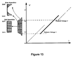
- Figure 13 shows how the pedestal voltage is adapted to ensure it is incremented with each subsegment ramp, ensuring it begins with a suitable overlap with the previous range by examining where in the hyperbins, the hits are occurring.
- the ramp gives hits which are both higher than and lower than the target range.
- the size of the ramp is restricted to less than twice the subrange, any hits from above the target range will fall into the adjacent even hyperbin set. Due to the rollover nature of the hyperbins, it is also true than any hits from below the target range will fall into the same even hyperbin set. No hits outside the target range fall within the odd hyperbin unless they are more than a full hyperbin width away. This is prohibited by control of the input signal and significant numbers doing so would indicate a gross ADC problem.
- the input ramp is run a predetermined number of times to ensure sufficient numbers of hits within all the hyperbin elements to alleviate the error effect of any noise.
- the total number of hits in the target range is now added to a running total number of all the hits within the converter's input range.
- some additional data is stored for later use in the test calculations, for example DNL and INL test calculations. This additional data includes but is not limited to the total hits in the bin range, the largest hits in any bin within the range and the smallest number of hits within the bin range.
- a running grand total number of hits is recorded indicating the total number of hits covering all the codes in all the bin ranges tested so far.
- the next step is to use the contents of the hyperbins to determine where to start the next input pedestal voltage.
- this is set to be 50% below the top of the current hyperbin range so it can run with a sufficient overlap. This is achieved by examining the contents of both hyperbins to determine the middle of the range hit by the current ramp and identify what fraction of the ramp must be set to target the middle. A smaller overlap can be used provided it is enough to cover noise and tolerance error.
- the input ramp signal is used to target the odd hyperbin
- this is achieved by finding the centre of the current input ramp range as shown in Figure 13 .
- the odd hyperbin has been approximately equally filled with hits
- the even bin has hits at either end but is nearly empty in the middle.
- the lower 13 elements of the even hyperbin have some hits and the upper 24 also have hits.
- the centre is therefore approximately the 50 th element from the start of the hits captured in the bins owing to the ramp.
- the DNL can be found by first taking the grand total number of hits found across all the codes in and dividing this by the total number of codes. This will be a 2 to the power n and is readily implemented as a simple shift right circuit. This total represents the expected number of hits for each every code if they were spread evenly as in an ideal ADC. For each targeted hyperbin range the minimum and maximum number of hits for any given code is stored earlier as the input signal was controlled to target different ranges. Each of these figures can now be checked to see whether any of the codes within a given range received too many or too few hits compared with the average number now known.
- a stored maximum of 150 hits would imply a DNL of +0.5LSBs while a stored minimum of 50 would be -0.5LSBs.
- the actual limit can have been programmed in earlier in the process to permit the limits to be varied. A simple pass or fail result can be issued at this stage. Alternatively more detailed characteristics can be achieved by varying the limits. This may allow a more accurate assessment of the limit at which performance breaks down.
- the INL can also be found. Typically, the INL tolerance is significantly higher than allowed DNL specification tolerance. Accurate measures of the slopes between known codes points on the ADC output code characteristic are stored for each range. These effectively determine the shape of the ADC under test in detail, at least at the limits of each range of codes that was stored. The gain and offset have already been calculated as described above so simple arithmetic can be used to predict the expected position of each code. Also stored previously was the maximum size of a given code and minimum size. While primarily used for the much tighter DNL calculation as described, these can be included in the INL calculation limits too. Thus, provided each stored range point is within the allowed tolerance of expected locations for the INL, the ADC INL can be said to be within specification. It is obvious to one skilled in the art that where necessary variants of the above calculation such as calculating and/or storing the slope of each sub-range, or storing the maximum deviation from the said slope could be implemented to enhance or refine the calculation further.
- Noise determination can be achieved by fixing a steady input voltage and examining the range of bins into which the ADC codes fall. The statistical nature will spread the ADC results due to the noise and the width will indicate the noise present. For Gaussian noise the hits will form a Gaussian spread across several bins and the standard deviation will indicate the root means square noise present. For low levels of noise below an LSB, a different method must be employed. In such cases all the hits will fall within a single bin or two adjacent bins for affixed input voltage. This is likely to be the case only for lower resolution converters where each LSB represents a sizeable step of perhaps a few millivolts. In such cases the ramp pedestal can be used to adjust the fixed voltage until the hits are approximately even spread across two adjacent bins.
- Incremental adjustments and repeated measurements of the ratio in adjacent bins is used until the ratio has changed to approximately 5/6 in one bin and 1/6 in the other.
- the voltage adjustment between these two points is one standard deviation also equivalent to the RMS noise in the signal.
- the offset may be determined by reading the ADC output when a null voltage (zero or zero differential) is applied. This can be done by applying a fixed DC Input signal to the ADC and recording sufficient hits to indicate the average voltage applied.
- An alternative approach is also feasible using a standard linear projection process between two measured points on the ADC characteristic can be used to estimate the offset, being the voltage above the origin the line intersect the y -axis at code equals zero. These points can be provided to the ADC input as constant dc input voltages from a reference voltage and a fraction of the reference voltage.
- the gain may be determined by processing the intermediate results from the histograms together with a separate calibration of the ramp using the BIST, reference voltage and a comparator.
- the offset is estimated as described above and the precise slope of the test ramp is calculated by ramping the test signal generator output through a lower and higher known reference voltage and timing the transition time.
- These lower and higher reference voltages may be derived directly by dividing down the reference voltage using a resistor or capacitor network, which have good matching characteristics. Note the comparator offset voltage has no effect on this measurement as it is included in both measures and is automatically cancelled by ramping from one to the other voltage.
- Variations and Improvements on the invention can include the designation of certain bins within the hyperbin range to accumulate hits from additional adjacent codes. This effectively compresses further the number of actual bins required to scan a given range. For example the last bin in hyper bin range might collect all the hits from the ADC codes relating to the following 16 ADC codes. This can have utility in the precision of joining the results from a given targeted subrange with the next targeted subrange. Similarly more than one bin can be used to accumulate hits for several ADC codes.
- the bins may be non-linearly compressed. For example, bins at the edges of the hyperbins may be arranged to receive hits for multiple codes, whereas bins in the middle of the hyperbin may accept hits from single codes.
- FIG 14 shows a pedestal voltage generator for use in the test of the present invention.
- This has a digital controller that is connected to a current source that feeds a capacitor (C1).
- C1 Connected across the capacitor C1 is a capacitor divider (C2, C3) to reduce the amplitude of the miniramp.
- Output from this part of the circuit is a voltage ramp.
- a further capacitor, C4 is connected on one side between the capacitors C2 and C3 and on the other side to the positive input of a unity gain buffer op amp. The capacitor C4 is used first to sample and then to eliminate an offset voltage of the buffer op amp.
- a capacitor Connected between the negative input of the buffer amp and its output is a capacitor, C5 which holds the current pedestal voltage. Not shown for the sake of simplicity and clarity in the figure are switches placed around C4, C5 to permit them to sample and hold offset and pedestal voltages. These switches are controllable by the digital controller.
- Connected between capacitor C5 and earth is a further capacitor C6. This can be positioned as shown in Figure 14 or switched with the capacitor C5, so that the capacitors alternately act as a pedestal hold voltage capacitor when in the feedback position shown as C5, and a pedestal voltage sampling capacitor that can be charged to a required level prior to switching into the feedback position when in the sampling position shown as C6. C5 and C6 alternately swap locations and roles. Thus a single ended pedestal based ramp generator analog circuit is implemented.
- the lower part of Figure 14 shows how the ramp circuit can be readily extended to a differential variant of the same circuit
- the pedestal capacitor is charged at the outset with a common mode voltage.
- the additional circuitry required for this differential variant comprises an inverter op amp stage, which is connected between the capacitor divider and the output pedestal buffer stage. Connected to the input of the inverter op amp is a capacitor C11. A further capacitor C12 is connected across the input terminal and the output.
- the ramp is provided to the negative input of a differential input converter while the original signal from the upper buffer is applied to the non-inverting input of the converter.
- the selection of the pedestal capacitor voltage on which to start the ramp can be simply the specified common mode voltage at which the ADC requires to be tested, or it can be the minimum permitted voltage for the converter positive input and the maximum permitted voltage for the negative input, permitting both outputs to ramp through their full range from maximum negative differential input voltage through zero to maximum positive differential input voltage.
- the current source and capacitor C1 are capable of generating a ramp, which due to real circuit limitations maintains only up to N, bits linearity over a restricted voltage range.
- N b bit multilevel pedestal voltage generator
- This circuit architecture allows the test stimulus to be sequentially incremented by successively sampling the present output voltage and bootstrapping this voltages by placing it on a feedback capacitor to create a DC level change between the inverting input and output terminals on a feedback circuit such as an op amp.
- each subsequent pedestal voltage is found by capturing a DC voltage during the ramping time of the previous DC shifted ramp output. This could be the peak of the previous DC shifted ramp, or halfway up the previous DC shifted ramp or some other percentage of the way up the previous DC shifted ramp.
- the choice of the DC voltage or pedestal voltage may be programmable through the digital section of the BIST by changing the sampling time. Inherent errors caused by capacitance variation with voltage C(V) are overcome because each pedestal capacitor voltage is driven and set by the op amp output which is a near unity gain voltage source independent of capacitor value or ratios.
- Each new pedestal voltage can be captured on a capacitor which can be used to form part of the voltage following level shift circuit. Since the voltage across the capacitor during the ramp does not change, no degradation of the circuit linearity occurs. Thus the pedestal voltage generator switches two identical capacitors for each output op amp. One provides a unity gain feedback path while the other is being charged. Then they switch roles and a new pedestal is formed. The op-amp offset voltage can also be removed by a calibration procedure permitting the hyperbins to create data which can later be processed accurately to determine the ADC offset voltage.
- each new pedestal voltage could also be created by a DAC or a resistor ladder network across the supplies, or any other appropriate method of generating a reasonably controlled voltage source. Although that would require additional hardware it would still retain the benefits of immunity to variation of capacitance with DC voltage across it, C(V), provided it is filled from a voltage source.
- the histogram method employs many ramps during the test. Variations, with time, which occur during the period of a full test in any of the ramps or other signals used for test purposes, such as non-stationary noise or interference or the effect of temperature changes on circuit components can be minimised by employing a suitable algorithm.
- the INL measurement can be improved by targeting the input signal at non-contiguous sections of the ADC. This is readily controlled using the digital control circuitry and ensures that no linearity error in the test stimulus is allowed to build up across the entire input range of the ADC which would degrade the INL measurement.
- a range with low ADC values may be targeted first, then a range with high ADC values, then a middle range, then a low range again and so on until the whole ADC input range has been covered.
- changing ranges is simply a matter of changing the pedestal voltage, for example as described elsewhere in this invention and a full set of ramps is applied to each range before moving onto the next as before. The same data for each section is described as before. In addition a not must be kept of which ranges have so far been targeted.
- the present invention uses a test algorithm that has been enhanced by exploiting as much digital circuitry in the algorithm as possible.
- the invention makes use of innovative analog circuit design to achieve extremely high effective-resolution when coupled with the digital circuitry.
- a software tool allows a designer to develop a test solution without detailed experience of one or more of the following: digital circuit design, analog circuit design, test engineering, thereby creating a full test solution simply by selecting options from a 'pushbutton' tool.
Landscapes
- Engineering & Computer Science (AREA)
- Theoretical Computer Science (AREA)
- Physics & Mathematics (AREA)
- Data Mining & Analysis (AREA)
- General Physics & Mathematics (AREA)
- Mathematical Optimization (AREA)
- Pure & Applied Mathematics (AREA)
- Mathematical Physics (AREA)
- Computational Mathematics (AREA)
- Mathematical Analysis (AREA)
- Algebra (AREA)
- Operations Research (AREA)
- Probability & Statistics with Applications (AREA)
- Bioinformatics & Cheminformatics (AREA)
- Bioinformatics & Computational Biology (AREA)
- Evolutionary Biology (AREA)
- Databases & Information Systems (AREA)
- Software Systems (AREA)
- General Engineering & Computer Science (AREA)
- Life Sciences & Earth Sciences (AREA)
- Analogue/Digital Conversion (AREA)
- Tests Of Electronic Circuits (AREA)
Applications Claiming Priority (1)
| Application Number | Priority Date | Filing Date | Title |
|---|---|---|---|
| US31435010P | 2010-03-16 | 2010-03-16 |
Publications (2)
| Publication Number | Publication Date |
|---|---|
| EP2372916A2 true EP2372916A2 (de) | 2011-10-05 |
| EP2372916A3 EP2372916A3 (de) | 2013-04-17 |
Family
ID=44486130
Family Applications (1)
| Application Number | Title | Priority Date | Filing Date |
|---|---|---|---|
| EP11250312.3A Withdrawn EP2372916A3 (de) | 2010-03-16 | 2011-03-16 | ADC-Test |
Country Status (2)
| Country | Link |
|---|---|
| US (2) | US8682613B2 (de) |
| EP (1) | EP2372916A3 (de) |
Cited By (5)
| Publication number | Priority date | Publication date | Assignee | Title |
|---|---|---|---|---|
| CN103475369A (zh) * | 2013-07-04 | 2013-12-25 | 东南大学 | 基于信号源误差一次性校准识别的高精度adc测试方法 |
| DE102015108045A1 (de) | 2014-05-26 | 2015-11-26 | Matthias Uhl | Vorrichtung zur Reinigung von Wäscherei Transport- und Lagersystemen |
| US9246503B1 (en) | 2013-09-09 | 2016-01-26 | Ateeda Ltd. | Built in self-test |
| US11018681B1 (en) | 2020-03-18 | 2021-05-25 | Analog Devices International Unlimited Company | Digital-to-analog converter waveform generator |
| US20230090369A1 (en) * | 2021-09-23 | 2023-03-23 | Noam Familia | Apparatus and method for clock phase calibration |
Families Citing this family (13)
| Publication number | Priority date | Publication date | Assignee | Title |
|---|---|---|---|---|
| TWI509553B (zh) * | 2012-11-23 | 2015-11-21 | Microip Inc | 製造電子單元的系統、電腦程式產品及其方法 |
| US9099173B2 (en) * | 2012-12-14 | 2015-08-04 | Virtium Technology, Inc. | Classifying flash devices using ECC |
| US8803716B1 (en) * | 2013-04-10 | 2014-08-12 | Stmicroelectronics International N.V. | Memoryless sliding window histogram based BIST |
| US20140306689A1 (en) | 2013-04-10 | 2014-10-16 | Texas Instruments, Incorporated | High resolution current pulse analog measurement |
| US8978005B2 (en) * | 2013-06-06 | 2015-03-10 | International Business Machines Corporation | Network reconfiguration in a data converter for improved electrical characteristics |
| US9240798B2 (en) * | 2014-02-28 | 2016-01-19 | Texas Instruments Incorporated | On-chip analog-to-digital converter (ADC) linearity text for embedded devices |
| US9645195B2 (en) * | 2014-05-27 | 2017-05-09 | Freescale Semiconductor, Inc. | System for testing integrated circuit |
| US9874607B1 (en) | 2016-03-24 | 2018-01-23 | Altera Corporation | Method and apparatus for using programmable logic circuitry to test on-chip analog-to-digital converter |
| US10892768B2 (en) * | 2017-09-11 | 2021-01-12 | Texas Instruments Incorporated | Low noise and low distortion test method and system for analog-to-digital converters |
| CN109727616A (zh) * | 2018-12-12 | 2019-05-07 | 珠海博雅科技有限公司 | 一种仿真mos管放大电路失调的方法及装置 |
| JP7412551B2 (ja) * | 2019-10-23 | 2024-01-12 | ホアウェイ・テクノロジーズ・カンパニー・リミテッド | 入力信号レベルシフトを有する適応相関多重サンプリング |
| US11196437B1 (en) * | 2020-12-01 | 2021-12-07 | Infineon Technologies Ag | System and method for testing an analog-to-digital converter |
| CN115327967A (zh) * | 2021-05-10 | 2022-11-11 | 天津普智芯网络测控技术有限公司 | 一种adc器件及dac器件验证方法 |
Citations (2)
| Publication number | Priority date | Publication date | Assignee | Title |
|---|---|---|---|---|
| US4897650A (en) | 1988-04-05 | 1990-01-30 | General Electric Company | Self-characterizing analog-to-digital converter |
| US6642870B1 (en) | 1999-09-09 | 2003-11-04 | Centre National De La Recherche Scientifique (C.N.R.S.) | Method and device for integrated testing for an analog-to-digital converter |
Family Cites Families (6)
| Publication number | Priority date | Publication date | Assignee | Title |
|---|---|---|---|---|
| US3931730A (en) * | 1974-12-23 | 1976-01-13 | The United States Of America As Represented By The Secretary Of The Army | Ramp current apparatus and method of sensitivity testing |
| US6798185B2 (en) * | 2002-06-28 | 2004-09-28 | International Business Machines Corporation | Method and apparatus for testing analog to digital converters |
| US7769110B2 (en) * | 2005-05-13 | 2010-08-03 | Broadcom Corporation | Threshold adjust system and method |
| US7583945B2 (en) * | 2006-01-10 | 2009-09-01 | Freescale Semiconductor, Inc. | Amplifier with improved noise performance and extended gain control range |
| US7561083B2 (en) * | 2007-10-31 | 2009-07-14 | Eagle Test Systems, Inc. | Testing of analog to digital converters |
| US8319509B1 (en) * | 2012-04-30 | 2012-11-27 | Atmel Corporation | Testing circuit for an analog to digital converter |
-
2011
- 2011-03-16 EP EP11250312.3A patent/EP2372916A3/de not_active Withdrawn
- 2011-03-16 US US13/049,494 patent/US8682613B2/en active Active
-
2014
- 2014-02-06 US US14/174,334 patent/US9106247B2/en active Active
Patent Citations (2)
| Publication number | Priority date | Publication date | Assignee | Title |
|---|---|---|---|---|
| US4897650A (en) | 1988-04-05 | 1990-01-30 | General Electric Company | Self-characterizing analog-to-digital converter |
| US6642870B1 (en) | 1999-09-09 | 2003-11-04 | Centre National De La Recherche Scientifique (C.N.R.S.) | Method and device for integrated testing for an analog-to-digital converter |
Cited By (9)
| Publication number | Priority date | Publication date | Assignee | Title |
|---|---|---|---|---|
| CN103475369A (zh) * | 2013-07-04 | 2013-12-25 | 东南大学 | 基于信号源误差一次性校准识别的高精度adc测试方法 |
| CN103475369B (zh) * | 2013-07-04 | 2016-08-10 | 东南大学 | 基于信号源误差一次性校准识别的高精度adc测试方法 |
| US9246503B1 (en) | 2013-09-09 | 2016-01-26 | Ateeda Ltd. | Built in self-test |
| US9705523B1 (en) | 2013-09-09 | 2017-07-11 | Ateeda Limited | Built in self-test |
| US9998133B2 (en) | 2013-09-09 | 2018-06-12 | Analog Devices, Inc. | Digital-to-analog converter waveform generator |
| DE102015108045A1 (de) | 2014-05-26 | 2015-11-26 | Matthias Uhl | Vorrichtung zur Reinigung von Wäscherei Transport- und Lagersystemen |
| US11018681B1 (en) | 2020-03-18 | 2021-05-25 | Analog Devices International Unlimited Company | Digital-to-analog converter waveform generator |
| US20230090369A1 (en) * | 2021-09-23 | 2023-03-23 | Noam Familia | Apparatus and method for clock phase calibration |
| US12381706B2 (en) * | 2021-09-23 | 2025-08-05 | Intel Corporation | Apparatus and method for clock phase calibration |
Also Published As
| Publication number | Publication date |
|---|---|
| US9106247B2 (en) | 2015-08-11 |
| US20110231153A1 (en) | 2011-09-22 |
| US20140203954A1 (en) | 2014-07-24 |
| US8682613B2 (en) | 2014-03-25 |
| EP2372916A3 (de) | 2013-04-17 |
Similar Documents
| Publication | Publication Date | Title |
|---|---|---|
| US9106247B2 (en) | ADC testing | |
| US10079610B2 (en) | Built-in self-test for ADC | |
| US8749422B1 (en) | Signal conversion using state sensitive device arrays | |
| JP2008157971A (ja) | サンプリングタイミング信号発生器 | |
| US7233274B1 (en) | Capacitive level shifting for analog signal processing | |
| US20090102517A1 (en) | Track-And-Hold Circuit With Adjustable Charge Compensation | |
| CN104297619A (zh) | 一种芯片输入输出管脚测试装置 | |
| US8723711B1 (en) | Stair-step voltage ramp module including programmable gain amplifier | |
| Provost et al. | Auto-calibrating analog timer for on-chip testing | |
| CN114157297B (zh) | 高精度模数转换芯片的测试装置和测试方法 | |
| Cai et al. | Peak detector with an FPGA-only solution for multichannel ultrafast signals | |
| JP4150402B2 (ja) | 信号波形測定装置及び信号波形測定システム | |
| Blair | Selecting test frequencies for two-tone phase plane analysis of ADC's | |
| Liaperdos et al. | A built-in voltage measurement technique for the calibration of RF mixers | |
| US10200055B2 (en) | Glitch characterization in digital-to-analog conversion | |
| Walker | A step response based mixed-signal BIST approach | |
| Mohan et al. | A code transition delay model for ADC test | |
| Barua et al. | A code width built-in-self test circuit for 8-bit pipelined ADC | |
| CN108681275B (zh) | 电压线性隔离调理电路输出电压参数化补偿方法与装置 | |
| Wan et al. | Reliability of SAR ADCs and associated embedded instrument detection | |
| Hemanthkumar | Implementation of Monotonicity Testing Utilizing On Chip Resources for Test Time Reduction | |
| Siddavatam et al. | A pulse generation system based on new method for testing performance of high-resolution nuclear spectroscopy systems | |
| Dhare et al. | SAF analyses of analog and mixed signal vlsi circuit: Digital to analog converter | |
| Li et al. | On-chip accumulated jitter measurement for phase-locked loops | |
| Abad et al. | Output Response Analyzer of Built-in-Self-Test for 14-Bit ADC in 0.13 µm CMOS Technology |
Legal Events
| Date | Code | Title | Description |
|---|---|---|---|
| PUAI | Public reference made under article 153(3) epc to a published international application that has entered the european phase |
Free format text: ORIGINAL CODE: 0009012 |
|
| AK | Designated contracting states |
Kind code of ref document: A2 Designated state(s): AL AT BE BG CH CY CZ DE DK EE ES FI FR GB GR HR HU IE IS IT LI LT LU LV MC MK MT NL NO PL PT RO RS SE SI SK SM TR |
|
| AX | Request for extension of the european patent |
Extension state: BA ME |
|
| RIC1 | Information provided on ipc code assigned before grant |
Ipc: H03M 1/10 20060101AFI20121120BHEP Ipc: H03M 1/12 20060101ALN20121120BHEP |
|
| PUAL | Search report despatched |
Free format text: ORIGINAL CODE: 0009013 |
|
| AK | Designated contracting states |
Kind code of ref document: A3 Designated state(s): AL AT BE BG CH CY CZ DE DK EE ES FI FR GB GR HR HU IE IS IT LI LT LU LV MC MK MT NL NO PL PT RO RS SE SI SK SM TR |
|
| AX | Request for extension of the european patent |
Extension state: BA ME |
|
| RIC1 | Information provided on ipc code assigned before grant |
Ipc: H03M 1/12 20060101ALN20130311BHEP Ipc: H03M 1/10 20060101AFI20130311BHEP |
|
| 17P | Request for examination filed |
Effective date: 20131015 |
|
| RBV | Designated contracting states (corrected) |
Designated state(s): AL AT BE BG CH CY CZ DE DK EE ES FI FR GB GR HR HU IE IS IT LI LT LU LV MC MK MT NL NO PL PT RO RS SE SI SK SM TR |
|
| 17Q | First examination report despatched |
Effective date: 20160728 |
|
| STAA | Information on the status of an ep patent application or granted ep patent |
Free format text: STATUS: THE APPLICATION IS DEEMED TO BE WITHDRAWN |
|
| 18D | Application deemed to be withdrawn |
Effective date: 20161208 |