EP2367211A2 - Light emitting diode and light emitting diode package - Google Patents
Light emitting diode and light emitting diode package Download PDFInfo
- Publication number
- EP2367211A2 EP2367211A2 EP11156264A EP11156264A EP2367211A2 EP 2367211 A2 EP2367211 A2 EP 2367211A2 EP 11156264 A EP11156264 A EP 11156264A EP 11156264 A EP11156264 A EP 11156264A EP 2367211 A2 EP2367211 A2 EP 2367211A2
- Authority
- EP
- European Patent Office
- Prior art keywords
- light emitting
- layer
- emitting device
- ohmic contact
- reflection layer
- Prior art date
- Legal status (The legal status is an assumption and is not a legal conclusion. Google has not performed a legal analysis and makes no representation as to the accuracy of the status listed.)
- Granted
Links
Images




Classifications
-
- H—ELECTRICITY
- H10—SEMICONDUCTOR DEVICES; ELECTRIC SOLID-STATE DEVICES NOT OTHERWISE PROVIDED FOR
- H10H—INORGANIC LIGHT-EMITTING SEMICONDUCTOR DEVICES HAVING POTENTIAL BARRIERS
- H10H20/00—Individual inorganic light-emitting semiconductor devices having potential barriers, e.g. light-emitting diodes [LED]
- H10H20/80—Constructional details
- H10H20/83—Electrodes
- H10H20/832—Electrodes characterised by their material
- H10H20/835—Reflective materials
-
- H—ELECTRICITY
- H10—SEMICONDUCTOR DEVICES; ELECTRIC SOLID-STATE DEVICES NOT OTHERWISE PROVIDED FOR
- H10H—INORGANIC LIGHT-EMITTING SEMICONDUCTOR DEVICES HAVING POTENTIAL BARRIERS
- H10H20/00—Individual inorganic light-emitting semiconductor devices having potential barriers, e.g. light-emitting diodes [LED]
- H10H20/80—Constructional details
- H10H20/83—Electrodes
- H10H20/832—Electrodes characterised by their material
- H10H20/833—Transparent materials
-
- H—ELECTRICITY
- H10—SEMICONDUCTOR DEVICES; ELECTRIC SOLID-STATE DEVICES NOT OTHERWISE PROVIDED FOR
- H10H—INORGANIC LIGHT-EMITTING SEMICONDUCTOR DEVICES HAVING POTENTIAL BARRIERS
- H10H20/00—Individual inorganic light-emitting semiconductor devices having potential barriers, e.g. light-emitting diodes [LED]
- H10H20/80—Constructional details
- H10H20/84—Coatings, e.g. passivation layers or antireflective coatings
- H10H20/841—Reflective coatings, e.g. dielectric Bragg reflectors
Definitions
- the present disclosure relates to a light emitting device and a light emitting device package.
- LED Light emitting diodes
- LEDs are semiconductor devices that convert electric energy into light. LEDs are more advantageous in many respects such as low power consumption, a semi-permanent life cycle, a fast response time, safety, and eco-friendly characteristics than light sources of the related art such as a fluorescent lamp and an incandescent bulb. Many studies have been conducted to replace existing light sources with LEDs, and LEDs are being increasingly used as light sources of lighting devices such as indoor and outdoor lamps, liquid crystal displays, electronic boards, and streetlights.
- Embodiments provide a light emitting device having improved light emitting efficiency.
- a light emitting device including: a transparent substrate; a light emitting structure including a first conductive type semiconductor layer, an active layer, and a second conductive type semiconductor layer that are disposed on a top surface of the substrate; and a first reflection layer on a bottom surface of the substrate, wherein the bottom surface of the substrate has a surface roughness of about 1 nm to about 15 nm in root mean square (RMS) value.
- RMS root mean square
- a light emitting device including: a conductive support member; a second reflection layer on the conductive support member; an ohmic contact layer disposed on the second reflection layer and having a rough bottom surface; and a light emitting structure including a first conductive type semiconductor layer, an active layer, and a second conductive type semiconductor layer that are disposed on the ohmic contact layer, wherein the bottom surface of the ohmic contact layer has a surface roughness in a range from about 1 nm to about 5 nm in RMS value.
- a light emitting device package including: a body part; first and second electrode layers on the body part; and a light emitting device electrically connected to the first and second electrode layers, wherein the light emitting device includes the light emitting device.
- embodiments provide a light emitting device having improved light emitting efficiency.
- Fig. 1 is a sectional view illustrating a light emitting device according to a first embodiment.
- Fig. 2 is an enlarge view of portion A of Fig. 1 .
- Fig. 3 is a graph illustrating results of an experiment carried out to measure reflection efficiency with respect to the surface roughness of a transparent substrate when the wavelength of light output from a light emitting structure of the light emitting device of Fig. 1 was in the range of about 380 nm to about 520 nm.
- Fig. 4 is a graph illustrating results of an experiment carried out to measure reflection efficiency with respect to the surface roughness of a transparent substrate when the wavelength of light emitted from the light emitting structure of the light emitting device of Fig. 1 was in the range of about 520 nm to about 700 nm.
- Fig. 5 is a sectional view illustrating a light emitting device according to a second embodiment.
- Fig. 6 is an enlarged view of portion B of Fig. 5 .
- Fig. 7 is a graph illustrating results of an experiment carried out to measure reflection efficiency with respect to the wavelength range of light emitted from a light emitting structure of the light emitting device of Fig. 5 when the surface roughness of an ohmic contact layer of the light emitting device was in the range of about 1 nm to about 3 nm in RMS vaue.
- Fig. 8 is a graph illustrating results of an experiment carried out to measure reflection efficiency with respect to the wavelength range of light output from the light emitting structure of the light emitting device of Fig. 5 when the surface roughness of the ohmic contact layer of the light emitting device was in the range of about 3 nm to about 5 nm in RMS value.
- Fig. 9 is a sectional view illustrating a light emitting device package including a light emitting device according to an embodiment.
- Fig. 10 is a view illustrating a backlight unit using light emitting device according to an embodiment.
- Fig. 11 is a view illustrating a lighting system using a light emitting device according to an embodiment.
- a layer (or film), a region, a pattern, or a structure is referred to as being on' a substrate, a layer (or film), a region, a pad, or patterns, it can be directly on another layer or substrate, or intervening layers may also be present. Further, it will be understood that when a layer is referred to as being 'under' another layer, it can be directly under another layer, and one or more intervening layers may also be present. Further, the reference about 'on' and 'under' each layer will be made on the basis of drawings.
- each layer is exaggerated, omitted, or schematically illustrated for convenience in description and clarity. Also, the size of each element does not entirely reflect an actual size.
- Fig. 1 is a sectional view illustrating a light emitting device 100 according to a first embodiment
- Fig. 2 is an enlarged view of portion A of Fig. 1 .
- the light emitting device 100 may include a first reflection layer 105, a transparent substrate 110 disposed on the first reflection layer 105, a light emitting structure 145 disposed on the transparent substrate 110 to generate light, and first and second electrodes 131 and 161 configured to supply power 161 to the light emitting structure 145.
- the transparent substrate 110 is a growth substrate on which the light emitting structure 145 grows.
- the transparent substrate 110 may be formed of a material such as Al 2 O 3 (sapphire), GaN, ZnO, and AlN.
- the light emitting structure 145 includes a plurality of compound semiconductor layers that generate light from electricity received through the first and second electrodes 131 and 161 by recombination of electrons and holes.
- the light emitting structure 145 may be formed of a compound semiconductor material having a compositional formula of In x Al y Ga 1-x-y N (0 ⁇ x ⁇ 1, 0 ⁇ y ⁇ 1, 0 ⁇ x+y ⁇ 1).
- the light emitting structure 145 may include a first semiconductor layer 130, an active layer 140 on the first semiconductor layer 130, and a second conductive type semiconductor layer 150 on the active layer 140.
- the first semiconductor layer 130 is formed of a first conductive type semiconductor layer.
- the first semiconductor layer 130 may further include an undoped semiconductor layer under the first conductive type semiconductor layer.
- the first semiconductor layer 130 is not limited thereto.
- the first conductive type semiconductor layer may include an n-type semiconductor layer.
- the n-type semiconductor layer may be formed of a semiconductor material having a compositional formula of In x Al y Ga 1-x-y N (0 ⁇ x ⁇ 1, 0 ⁇ y ⁇ 1, 0 ⁇ x+y ⁇ 1) such as GaN, AlN, AlGaN, InGaN, InN, InAlGaN, and AlInN.
- the n-type semiconductor layer may be doped with an n-type dopent such as Si, Ge, and Sn.
- the undoped semiconductor layer may be provided to improve crystallization of the first conductive type semiconductor layer.
- the undoped semiconductor layer may be the same as the first conductive type semiconductor layer except that the undoped semiconductor layer has a very low conductivity because it is not doped.
- the active layer 140 may include a semiconductor material including a compositional formula of In x Al y Ga 1-x-y N (0 ⁇ x ⁇ 1, 0 ⁇ y ⁇ 1, 0 ⁇ x+y ⁇ 1).
- the active layer 140 may has one of a single quantum well structure, a multi quantum well (MQW) structure, a quantum wire structure, and a quantum dot structure.
- MQW multi quantum well
- the active layer 140 may have a single or multi quantum well structure including a well lay of In x Al y Ga 1-x-y N (0 ⁇ x ⁇ 1, 0 ⁇ y ⁇ 1, 0 ⁇ x+y ⁇ 1) and a barrier layer of In a Al b Ga 1-a-b N (0 ⁇ a ⁇ 1, 0 ⁇ b ⁇ 1, 0 ⁇ a+b ⁇ 1).
- the well layer may be formed of a material having an energy band gap smaller than that of the barrier layer.
- the active layer 140 may emit light by using energy generated during recombination of electrons and holes received from the first semiconductor layer 130 and the second conductive type semiconductor layer 150.
- the second conductive type semiconductor layer 150 may be realized by a p-type semiconductor layer.
- the p-type semiconductor layer may be formed of a semiconductor material having a compositional formula of In x Al y Ga 1-x-y N (0 ⁇ x ⁇ 1, 0 ⁇ y ⁇ 1, 0 ⁇ x+y ⁇ 1) such as GaN, AlN, AlGaN, InGaN, InN, InAlGaN, and AlInN.
- the second conductive type semiconductor layer 150 may be doped with a p-type dopant such as Mg, Zn, Ca, Sr, and Ba.
- the first electrode 131 may be formed on the first semiconductor layer 130, and the second electrode 161 may be formed on the second conductive type semiconductor layer 150, to supply power to the light emitting structure 145.
- the first and second electrodes 131 and 161 may include at least one of aluminum (Al), titanium (Ti), chromium (Cr), nickel (Ni), copper (Cu), and gold (Au).
- a transparent electrode layer 160 may be further disposed between the second electrode 161 and the light emitting structure 145.
- the transparent electrode layer 160 may include at least one of ITO, IZO (In-ZnO), GZO (Ga-ZnO), AZO (Al-ZnO), AGZO (Al-Ga ZnO), IGZO (In-Ga ZnO), IrOx, RuOx, RuOx/ITO, Ni/IrOx/Au, and Ni/IrOx/Au/ITO.
- Light generated by the active layer 140 of the light emitting structure 145 may exit from the light emitting structure 145 through the top and side surfaces of the light emitting device 100.
- a concave-convex or rough structure (not shown) may be formed on the top surface and/or the side surfaces of the light emitting device 100 to improve light extraction efficiency.
- Light emitted downward from the light emitting structure 145 and passing through the first semiconductor layer 130 and the transparent substrate 110 has to be reflected to the top or side surfaces of the light emitting device 100 so that the light can exit to the outside of the light emitting device 100.
- the first reflection layer 105 is provided to efficiently reflect light emitting from the light emitting structure 145 to the outside of the light emitting device 100.
- the first reflection layer 105 may be formed on a bottom surface 110a of the transparent substrate 110 entirely or partially by a deposition or plating method.
- the first reflection layer 105 may be formed to a thickness of several micrometers ( ⁇ m) or more.
- the bottom surface 110a of the transparent substrate 110 may be roughened.
- the reflection efficiency of an interface between the transparent substrate 110 and the first reflection layer 105 may be highest.
- the bottom surface 110a of the transparent substrate 110 is somewhat rough, and although the bottom surface 110a of the transparent substrate 110 is polished by a polishing apparatus, its surface roughness is at least several nanometers (nm).
- a material of the first reflection layer 105 is selectively determined according to the surface roughness of the bottom surface 110a of the transparent substrate 110 and the wavelength range of light output from the light emitting structure 145.
- Fig. 3 is a graph illustrating results of an experiment carried out to measure reflection efficiency with respect to the surface roughness of the transparent substrate 110 when the wavelength of light emitted from the light emitting structure 145 was in the range of about 380 nm to about 520 nm
- Fig. 4 is a graph illustrating results of an experiment carried out to measure reflection efficiency with respect to the surface roughness of the transparent substrate 110 when the wavelength of light emitted from the light emitting structure 145 was in the range of about 520 nm to about 700 nm.
- a sapphire (Al 2 O 3 ) substrate was used as the transparent substrate 110, and the surface roughness of the transparent substrate 110 was measured in root mean square (RMS) value by using a surface roughness measuring device.
- RMS root mean square
- the reflection efficiency of the first reflection layer 105 is higher when the first reflection layer 105 includes silver (Ag) than when the first reflection layer 105 includes aluminum (Al).
- the reflectance of the first reflection layer 105 is almost about 80% or higher in the wavelength range of about 380 nm to about 520 nm.
- the reflection efficiency of the first reflection layer 105 is higher when the first reflection layer 105 includes aluminum (Al) than when the first reflection layer 105 includes silver (Ag).
- the reflectance of the first reflection layer 105 is almost about 80% or higher in the wavelength range of about 380 nm to about 520 nm.
- the reflection efficiency of the first reflection layer 105 is higher when the first reflection layer 105 includes silver (Ag) than when the first reflection layer 105 includes aluminum (Al).
- the first reflection layer 105 includes silver (Ag)
- the reflectance of the first reflection layer 105 is almost about 85% or higher in the wavelength range of about 520 nm to about 700 nm.
- the reflectance of the first reflection layer 105 is almost about 90% or higher in the wavelength range of about 520 nm to about 700 nm.
- a material for the first reflection layer 105 may be selected from one of silver (Ag) and aluminum (Al) which results in higher reflectance according to the wavelength range of light output from the light emitting structure 145 and the surface roughness of the bottom surface 110a of the transparent substrate 110.
- the bottom surface of a substrate may be roughened before or after compound semiconductor layers are grown, and a first reflection layer may be formed on the bottom surface of the substrate after the compound semiconductor layers are grown.
- Fig. 2 is a sectional view illustrating a light emitting device 200 according to a second embodiment, and Fig. 2 is an enlarged view of portion B of Fig. 5 .
- the light emitting device 200 may include a conductive support member 170, a second reflection layer 165 on the conductive support member 170, an ohmic contact layer 163 on the second reflection layer 165, a light emitting structure 145 on the ohmic contact layer 163, and a third electrode 180.
- the conductive support member 170 supports the light emitting structure 145 and is used to supply power to the light emitting device 200 together with the third electrode 180.
- the conductive support member 170 may include at least one of titanium (Ti), chromium (Cr), nickel (Ni), aluminum (Al), platinum (Pt), gold (Au), tungsten (W), copper (Cu), molybdenum (Mo), and a carrier wafer (formed of a material such as Si, Ge, GaAs, ZnO, SiC, SiGe, and GaN).
- the conductive support member 170 is generally formed of an opaque material, the light emitting efficiency of the light emitting device 100 can be improved by forming the second reflection layer 165 between the conductive support member 170 and the light emitting structure 145.
- the conductive support member 170 may be formed by a deposition method such as sputtering, plasma-enhanced chemical vapor deposition (PECVD), and E-beam deposition.
- a deposition method such as sputtering, plasma-enhanced chemical vapor deposition (PECVD), and E-beam deposition.
- PECVD plasma-enhanced chemical vapor deposition
- E-beam deposition the method of forming the conductive support member 170 is not limited thereto.
- the ohmic contact layer 163 may be provided to form an ohmic contact between the second reflection layer 165 and the light emitting structure 145.
- the ohmic contact layer 163 may be formed of a transparent ohmic contact material such as ITO, IZO (In-ZnO), GZO (Ga-ZnO), AZO (Al-ZnO), AGZO (Al-Ga ZnO), IGZO (In-Ga ZnO), IrOx, RuOx, and RuOx/ITO.
- the ohmic contact layer 163 may be formed of an ohmic metal such as Ni, Pt, Ir, Rh, and Ag. In this case, the ohmic contact layer 163 may be formed to a very thin thickness less than about several nanometers (nm), and thus the ohmic contact layer 163 may be substantially transparent.
- the ohmic contact layer 163 may be formed by a deposition method such as sputtering, PECVD, and E-beam deposition.
- a deposition method such as sputtering, PECVD, and E-beam deposition.
- the method of forming the ohmic contact layer 163 is not limited thereto.
- the bottom surface 163a of the ohmic contact layer 163 may be roughened. Since the rough bottom surface 163a of the ohmic contact layer 163 is located between the second reflection layer 165 and the ohmic contact layer 163, the reflection efficiency of the second reflection layer 165 may be affected by the rough bottom surface 163a.
- the rough bottom surface 163a of the ohmic contact layer 163 is formed while the ohmic contact layer 163 is deposited, and the surface roughness of the rough bottom surface 163a may be determined by, for example, a deposition apparatus, a deposition method, and a deposition thickness.
- a material of the second reflection layer 165 is selectively determined according to the surface roughness of the bottom surface 163a of the ohmic contact layer 163 and the wavelength range of light output from the light emitting structure 145.
- Fig. 7 is a graph illustrating results of an experiment carried out to measure reflection efficiency with respect to the wavelength range of light output from the light emitting structure 145 when the surface roughness of the ohmic contact layer 163 was in the range of about 1 nm to about 3 nm in RMS value
- Fig. 8 is a graph illustrating results of an experiment carried out to measure reflection efficiency with respect to the wavelength range of light output from the light emitting structure 145 when the surface roughness of the ohmic contact layer 163 was in the range of about 3 nm to about 5 nm in RMS value.
- the ohmic contact layer 163 was formed of ITO (Indium-Tin-Oxide).
- the ohmic contact layer 163 was formed by an E-beam deposition method. If the ohmic contact layer 163 is formed to a thickness of about 80 nm to about 120 nm, for example, about 100 nm, the surface roughness of the ohmic contact layer 163 may be adjusted to be in the range from about 1 nm to about 3 nm in RMS value. If the ohmic contact layer 163 is formed to a thickness of about 180 nm to about 220 nm, for example, about 200 nm, the surface roughness of the ohmic contact layer 163 may be adjusted to be in the range from about 3 nm to about 5 nm in RMS value. That is, the surface roughness of the ohmic contact layer 163 may be increased according to the thickness of the ohmic contact layer 163.
- the reflection efficiency of the second reflection layer 165 is higher when the second reflection layer 165 includes aluminum (Al) than when the second reflection layer 165 includes silver (Ag).
- the reflectance of the second reflection layer 165 is almost about 75% or higher in the wavelength range of about 400 nm to about 650 nm.
- the reflection efficiency of the second reflection layer 165 is higher when the second reflection layer 165 includes silver (Ag) than when the second reflection layer 165 includes aluminum (Al). In this case, the reflectance of the second reflection layer 165 is almost about 80% or higher.
- the reflection efficiency of the second reflection layer 165 is higher when the second reflection layer 165 includes aluminum (Al) than when the second reflection layer 165 includes silver (Ag).
- the reflectance of the second reflection layer 165 is almost about 75% or higher in the wavelength range of about 400 nm to about 650 nm.
- the reflection efficiency of the second reflection layer 165 is higher when the second reflection layer 165 includes silver (Ag) than when the second reflection layer 165 includes aluminum (Al). At this time, the reflectance of the second reflection layer 165 is almost about 80% or higher.
- a material for the second reflection layer 165 may be selected from one of silver (Ag) and aluminum (Al) which results in higher reflectance according to the wavelength range of light output from the light emitting structure 145 and the surface roughness of the bottom surface 163a of the ohmic contact layer 163.
- the light emitting structure 145 has the same structure as that of the first embodiment. Thus, a detailed description thereof will not be repeated. Hover, the light emitting structure 145 may have a reversed structure as compared with that of the light emitting structure 145 of the first embodiment. That is, the light emitting structure 145 may include a second conductive type semiconductor layer 150, an active layer 140 on the second conductive type semiconductor layer 150, and a first semiconductor layer 130 on the active layer 140.
- the third electrode 180 may be formed on the light emitting structure 145 to supply power to the light emitting structure 145.
- the third electrode 180 may be formed of the same material as that used to form the first and second electrodes 131 and 161 of the first embodiment.
- Fig. 9 is a sectional view illustrating a light emitting device package including the light emitting device 100 according to an embodiment.
- the light emitting device package of the current embodiment includes: a body part 20; first and second electrode layers 31 and 32 disposed on the body part 20; the light emitting device 100 of the previous embodiment disposed on the body part 20 and electrically connected to the first and second electrode layers 31 and 32; and a molding member 40 enclosing the light emitting device 100.
- the body part 20 may be formed of a silicon material, a synthetic resin material, or a metal material. Also, a sloped surface may be disposed around the light emitting device 100.
- the first and second electrode layers 31 and 32 are electrically separated from each other to supply power to the light emitting device 100.
- the first and second electrode layers 31 and 32 may reflect light emitted from the light emitting device 100 to improve optical efficiency and may dissipate heat generated from the light emitting device 100 the outside.
- the light emitting device 100 may be disposed on the body part 20 or the first or second electrode layer 31 or 32.
- a wiring method is used to electrically connect the light emitting device 100 to the first and second electrode layers 31 and 32.
- the connection method is not limited thereto.
- the light emitting device 100 may be electrically connected to the first and second electrode layers 31 and 32 through a flip chip method or a die bonding method.
- the molding member 40 may surround the light emitting device 100 to protect the light emitting device 100.
- a phosphor may be contained in the molding member 40 to change the wavelength of light emitted from the light emitting device 100.
- At least one of the light emitting devices of the above-described embodiments may be mounted in one or plurality on the light emitting device package.
- the light emitting device package is not limited thereto.
- a plurality of light emitting devices or light emitting device packages of the embodiments may be arrayed on a substrate.
- Optical members such as a light guide panel (LGP), a prism sheet, and a diffusion sheet may be disposed on optical paths of the light emitting device packages.
- the light emitting device packages, the substrate, and the optical members may function as a light unit.
- the semiconductor light emitting devices or the light emitting device packages of the above-described embodiments may be used in a display, an indicator, or a lighting system according to another embodiment. Examples of the light system include a lamp, a streetlight, an electronic board, and a headlamp of a vehicle.
- Fig. 10 is a view illustrating a backlight unit using light emitting devices according to an embodiment.
- the backlight unit of Fig. 10 is an example of light units. That is, the spirit and scope of the present disclosure is not limited thereto.
- the backlight unit may include a bottom cover 1400, a light guide member 1100 disposed within the bottom cover 1400, and a light emitting module 1000 disposed on at least one side surface or the bottom surface of the light guide member 1100. Also, a reflection sheet 1300 may be disposed under the light guide member 1100.
- the bottom cover 1400 may have a box shape with an opened top side to receive the light guide member 1100, the light emitting module 1000, and the reflective sheet 1300.
- the bottom cover 1400 may be formed of a metal material or a resin material, but is not limited thereto.
- the light emitting module 1000 may include a substrate and a plurality of light emitting device packages of the embodiment.
- the light emitting device packages may be disposed on the substrate.
- the light emitting device packages of the embodiment may provide light to the light guide member 1100.
- the light emitting module 1000 may be disposed on at least one of inner side surfaces of the bottom cover 1400. Thus, the light emitting module 1000 may provide light toward the inner side surface of the light guide member 1100.
- the light emitting module 1000 may be disposed on the bottom surface of the bottom cover 1400 to provide light toward the bottom surface of the light guide member 1100.
- This may be variously varied according to the design of the backlight unit. That is, the spirit and scope of the present disclosure is not limited thereto.
- the light guide member 1100 may be disposed within the bottom cover 1400.
- the light guide member 1100 may receive light from the light emitting module 1000 and guide the light to a display panel (not shown) as surface light.
- the light guide member 1100 may be a light guide panel (LGP).
- the LGP may be formed of an acryl-based resin such as polymethylmethacrylate (PMMA) or one of polyethylene terephthlate (PET), poly carbonate (PC), cyclic olefin copolymer (COC), and polyethylene naphthalate (PEN).
- PMMA polymethylmethacrylate
- PET polyethylene terephthlate
- PC poly carbonate
- COC cyclic olefin copolymer
- PEN polyethylene naphthalate
- the light guide member 1100 may include at least one of an LGP or an optical sheet.
- the optical sheet may include at least one of a diffusion sheet, a condensing sheet, and a brightness enhancement sheet.
- the optical sheet may be formed by sequentially stacking such a diffusion sheet, a condensing sheet, and a brightness enhancement sheet.
- the diffusion sheet may uniformly diffuse light output from the light emitting module 1000, and the diffused light may be condensed on a display panel (not shown) by the condensing sheet.
- light output through the condensing sheet is randomly polarized light.
- the brightness enhancement sheet may enhance polarization of the light output through the condensing sheet.
- the condensing sheet may be a horizontal and/or vertical prism sheet.
- the brightness enhancement sheet may be a dual brightness enhancement film.
- the reflection sheet 1300 may be disposed under the light guide member 1100.
- the reflection sheet 1300 may reflect light emitted through the bottom surface of the light guide member 1100 toward a light exit surface of the light guide member 1100.
- the reflection sheet 1300 may be formed of a resin material having a high reflectance such as PET, PC, and PVC, but is not limited thereto.
- Fig. 11 is a perspective view illustrating a lighting unit 1100 using light emitting device packages 200 according to an embodiment.
- the light unit of Fig. 11 is an example of lighting units. That is, the spirit and scope of the present disclosure is not limited thereto.
- the lighting unit 1100 may include a case body 1110, a light emitting module part 1130 disposed in the case body 1110, and a connection terminal 1120 disposed on the case body 1110 to receive power from an external power supply.
- the case body 1110 may be formed of a material having good heat dissipation characteristics, such as a metal material or a resin material.
- the light emitting module part 1130 may include a substrate 1132 and at least one light emitting device package 200 of the above-described embodiment.
- the light emitting device package 200 may be disposed on the substrate 1132.
- the substrate 1132 may be a substrate in which circuit patterns are printed on an insulator.
- Examples of the substrate 1132 may include a general printed circuit board (PCB), a metal core PCB, a flexible PCB, and a ceramic PCB.
- the substrate 1132 may be formed of a material capable of efficiently reflecting light.
- the substrate 1132 may have a surface having a color capable of efficiently reflecting light, such as a white color, or a silver color.
- the at least one light emitting device package 200 may be disposed on the substrate 1132.
- the light emitting device package 200 may include at least one light emitting diode (LED).
- the LED may include a color diode capable of emitting color such as red, green, blue, or white light, and an ultraviolet (UV) LED capable of emitting a UV ray.
- UV ultraviolet
- the light emitting module part 1130 may include a combination of various light emitting devices to obtain desired color tone and brightness.
- the light emitting module part 1130 may include a combination of a white LED, a red LED, and a green LED to secure a high color rendering index (CRI).
- CRI color rendering index
- connection terminal 1120 may be electrically connected to the light emitting module part 1130 to supply power. As shown in Fig. 11 , the connection terminal 1120 may be screwed and coupled to a socket of an external power source, but is not limited thereto. For example, the connection terminal 1120 may be formed in a pin shape. In this case, the connection terminal 1120 may be inserted into an external power source or connected to the external power source by using a cable.
- first and second can be selectively or exchangeably used for the members.
- a dimension of each of elements may be exaggerated for clarity of illustration, and the dimension of each of the elements may be different from an actual dimension of each of the elements.
- Not all elements illustrated in the drawings must be included and limited to the present disclosure, but the elements except essential features of the present disclosure may be added or deleted.
- each layer (or film), a region, a pattern, or a structure is referred to as being 'on/above/over/upper' substrate, each layer (or film), a region, a pad, or patterns, it can be directly on substrate each layer (or film), the region, the pad, or the patterns, or intervening layers may also be present.
- a layer is referred to as being 'under/below/lower' each layer (film), the region, the pattern, or the structure, it can be directly under another layer (film), another region, another pad, or another patterns, or one or more intervening layers may also be present. Therefore, meaning thereof should be judged according to the spirit of the present disclosure.
Landscapes
- Led Devices (AREA)
- Led Device Packages (AREA)
Abstract
Description
- The present application claims priority under 35 U.S.C. 119 and 35 U.S.C. 365 to Korean Patent Application No.
10-2010-0023736 (filed on March 17, 2010 - The present disclosure relates to a light emitting device and a light emitting device package.
- Light emitting diodes (LED) are semiconductor devices that convert electric energy into light. LEDs are more advantageous in many respects such as low power consumption, a semi-permanent life cycle, a fast response time, safety, and eco-friendly characteristics than light sources of the related art such as a fluorescent lamp and an incandescent bulb. Many studies have been conducted to replace existing light sources with LEDs, and LEDs are being increasingly used as light sources of lighting devices such as indoor and outdoor lamps, liquid crystal displays, electronic boards, and streetlights.
- Embodiments provide a light emitting device having improved light emitting efficiency.
- In one embodiment, a light emitting device including: a transparent substrate; a light emitting structure including a first conductive type semiconductor layer, an active layer, and a second conductive type semiconductor layer that are disposed on a top surface of the substrate; and a first reflection layer on a bottom surface of the substrate, wherein the bottom surface of the substrate has a surface roughness of about 1 nm to about 15 nm in root mean square (RMS) value.
- In another embodiment, a light emitting device including: a conductive support member; a second reflection layer on the conductive support member; an ohmic contact layer disposed on the second reflection layer and having a rough bottom surface; and a light emitting structure including a first conductive type semiconductor layer, an active layer, and a second conductive type semiconductor layer that are disposed on the ohmic contact layer, wherein the bottom surface of the ohmic contact layer has a surface roughness in a range from about 1 nm to about 5 nm in RMS value.
- In further another embodiment, a light emitting device package including: a body part; first and second electrode layers on the body part; and a light emitting device electrically connected to the first and second electrode layers, wherein the light emitting device includes the light emitting device.
- Therefore, embodiments provide a light emitting device having improved light emitting efficiency.
- The details of one or more embodiments are set forth in the accompanying drawings and the description below. Other features will be apparent from the description and drawings, and from the claims.
-
Fig. 1 is a sectional view illustrating a light emitting device according to a first embodiment. -
Fig. 2 is an enlarge view of portion A ofFig. 1 . -
Fig. 3 is a graph illustrating results of an experiment carried out to measure reflection efficiency with respect to the surface roughness of a transparent substrate when the wavelength of light output from a light emitting structure of the light emitting device ofFig. 1 was in the range of about 380 nm to about 520 nm. -
Fig. 4 is a graph illustrating results of an experiment carried out to measure reflection efficiency with respect to the surface roughness of a transparent substrate when the wavelength of light emitted from the light emitting structure of the light emitting device ofFig. 1 was in the range of about 520 nm to about 700 nm. -
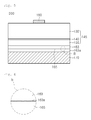
Fig. 5 is a sectional view illustrating a light emitting device according to a second embodiment. -
Fig. 6 is an enlarged view of portion B ofFig. 5 . -
Fig. 7 is a graph illustrating results of an experiment carried out to measure reflection efficiency with respect to the wavelength range of light emitted from a light emitting structure of the light emitting device ofFig. 5 when the surface roughness of an ohmic contact layer of the light emitting device was in the range of about 1 nm to about 3 nm in RMS vaue. -
Fig. 8 is a graph illustrating results of an experiment carried out to measure reflection efficiency with respect to the wavelength range of light output from the light emitting structure of the light emitting device ofFig. 5 when the surface roughness of the ohmic contact layer of the light emitting device was in the range of about 3 nm to about 5 nm in RMS value. -
Fig. 9 is a sectional view illustrating a light emitting device package including a light emitting device according to an embodiment. -
Fig. 10 is a view illustrating a backlight unit using light emitting device according to an embodiment. -
Fig. 11 is a view illustrating a lighting system using a light emitting device according to an embodiment. - In the descriptions of embodiments, it will be understood that when a layer (or film), a region, a pattern, or a structure is referred to as being on' a substrate, a layer (or film), a region, a pad, or patterns, it can be directly on another layer or substrate, or intervening layers may also be present. Further, it will be understood that when a layer is referred to as being 'under' another layer, it can be directly under another layer, and one or more intervening layers may also be present. Further, the reference about 'on' and 'under' each layer will be made on the basis of drawings.
- In the drawings, the thickness or size of each layer is exaggerated, omitted, or schematically illustrated for convenience in description and clarity. Also, the size of each element does not entirely reflect an actual size.
- Hereinafter, with reference to the accompanying drawings, a light emitting device and a light emitting device package will be described according to exemplary embodiments.
- <First embodiment>
-
Fig. 1 is a sectional view illustrating alight emitting device 100 according to a first embodiment, andFig. 2 is an enlarged view of portion A ofFig. 1 . - Referring to
Figs. 1 and 2 , thelight emitting device 100 may include afirst reflection layer 105, atransparent substrate 110 disposed on thefirst reflection layer 105, alight emitting structure 145 disposed on thetransparent substrate 110 to generate light, and first andsecond electrodes power 161 to thelight emitting structure 145. - The
transparent substrate 110 is a growth substrate on which thelight emitting structure 145 grows. For example, thetransparent substrate 110 may be formed of a material such as Al2O3 (sapphire), GaN, ZnO, and AlN. - The
light emitting structure 145 includes a plurality of compound semiconductor layers that generate light from electricity received through the first andsecond electrodes light emitting structure 145 may be formed of a compound semiconductor material having a compositional formula of InxAlyGa1-x-yN (0≤x≤1, 0≤y≤1, 0≤x+y≤1). - For example, the
light emitting structure 145 may include afirst semiconductor layer 130, anactive layer 140 on thefirst semiconductor layer 130, and a second conductivetype semiconductor layer 150 on theactive layer 140. - The
first semiconductor layer 130 is formed of a first conductive type semiconductor layer. Thefirst semiconductor layer 130 may further include an undoped semiconductor layer under the first conductive type semiconductor layer. However, thefirst semiconductor layer 130 is not limited thereto. - For example, the first conductive type semiconductor layer may include an n-type semiconductor layer. The n-type semiconductor layer may be formed of a semiconductor material having a compositional formula of InxAlyGa1-x-yN (0≤x≤1, 0 ≤y≤1, 0≤x+y≤1) such as GaN, AlN, AlGaN, InGaN, InN, InAlGaN, and AlInN. The n-type semiconductor layer may be doped with an n-type dopent such as Si, Ge, and Sn.
- The undoped semiconductor layer may be provided to improve crystallization of the first conductive type semiconductor layer. The undoped semiconductor layer may be the same as the first conductive type semiconductor layer except that the undoped semiconductor layer has a very low conductivity because it is not doped.
- The
active layer 140 may include a semiconductor material including a compositional formula of InxAlyGa1-x-yN (0≤x≤1, 0 ≤y≤1, 0≤x+y≤1). Theactive layer 140 may has one of a single quantum well structure, a multi quantum well (MQW) structure, a quantum wire structure, and a quantum dot structure. - If the
active layer 140 has a quantum well structure, theactive layer 140 may have a single or multi quantum well structure including a well lay of InxAlyGa1-x-yN (0≤x≤1, 0 ≤y≤1, 0≤x+y≤1) and a barrier layer of InaAlbGa1-a-bN (0≤a≤1, 0 ≤b≤1, 0≤a+b≤1). The well layer may be formed of a material having an energy band gap smaller than that of the barrier layer. - The
active layer 140 may emit light by using energy generated during recombination of electrons and holes received from thefirst semiconductor layer 130 and the second conductivetype semiconductor layer 150. - For example, the second conductive
type semiconductor layer 150 may be realized by a p-type semiconductor layer. The p-type semiconductor layer may be formed of a semiconductor material having a compositional formula of InxAlyGa1-x-yN (0≤x≤1, 0 ≤y≤1, 0≤x+y≤1) such as GaN, AlN, AlGaN, InGaN, InN, InAlGaN, and AlInN. The second conductivetype semiconductor layer 150 may be doped with a p-type dopant such as Mg, Zn, Ca, Sr, and Ba. - The
first electrode 131 may be formed on thefirst semiconductor layer 130, and thesecond electrode 161 may be formed on the second conductivetype semiconductor layer 150, to supply power to thelight emitting structure 145. The first andsecond electrodes - A transparent electrode layer 160 may be further disposed between the
second electrode 161 and thelight emitting structure 145. The transparent electrode layer 160 may include at least one of ITO, IZO (In-ZnO), GZO (Ga-ZnO), AZO (Al-ZnO), AGZO (Al-Ga ZnO), IGZO (In-Ga ZnO), IrOx, RuOx, RuOx/ITO, Ni/IrOx/Au, and Ni/IrOx/Au/ITO. - Light generated by the
active layer 140 of thelight emitting structure 145 may exit from thelight emitting structure 145 through the top and side surfaces of thelight emitting device 100. A concave-convex or rough structure (not shown) may be formed on the top surface and/or the side surfaces of thelight emitting device 100 to improve light extraction efficiency. - Light emitted downward from the
light emitting structure 145 and passing through thefirst semiconductor layer 130 and thetransparent substrate 110 has to be reflected to the top or side surfaces of thelight emitting device 100 so that the light can exit to the outside of thelight emitting device 100. - In the embodiment, the
first reflection layer 105 is provided to efficiently reflect light emitting from thelight emitting structure 145 to the outside of thelight emitting device 100. - The
first reflection layer 105 may be formed on abottom surface 110a of thetransparent substrate 110 entirely or partially by a deposition or plating method. Thefirst reflection layer 105 may be formed to a thickness of several micrometers (µm) or more. - As shown in
Fig. 2 , thebottom surface 110a of thetransparent substrate 110 may be roughened. - Ideally, when the
bottom surface 110a of thetransparent substrate 110 is perfectly smooth (surface roughness is zero), the reflection efficiency of an interface between thetransparent substrate 110 and thefirst reflection layer 105 may be highest. - However, practically, the
bottom surface 110a of thetransparent substrate 110 is somewhat rough, and although thebottom surface 110a of thetransparent substrate 110 is polished by a polishing apparatus, its surface roughness is at least several nanometers (nm). - In the embodiment, a material of the
first reflection layer 105 is selectively determined according to the surface roughness of thebottom surface 110a of thetransparent substrate 110 and the wavelength range of light output from thelight emitting structure 145. -
Fig. 3 is a graph illustrating results of an experiment carried out to measure reflection efficiency with respect to the surface roughness of thetransparent substrate 110 when the wavelength of light emitted from thelight emitting structure 145 was in the range of about 380 nm to about 520 nm, andFig. 4 is a graph illustrating results of an experiment carried out to measure reflection efficiency with respect to the surface roughness of thetransparent substrate 110 when the wavelength of light emitted from thelight emitting structure 145 was in the range of about 520 nm to about 700 nm. - In the experiments, a sapphire (Al2O3) substrate was used as the
transparent substrate 110, and the surface roughness of thetransparent substrate 110 was measured in root mean square (RMS) value by using a surface roughness measuring device. - Referring to
Fig. 3 , when the wavelength of light emitted from thelight emitting structure 145 is in the range from about 380 nm to about 520 nm and the surface roughness of thebottom surface 110a of thetransparent substrate 110 is in the range from about 1 nm to about 10 nm, the reflection efficiency of thefirst reflection layer 105 is higher when thefirst reflection layer 105 includes silver (Ag) than when thefirst reflection layer 105 includes aluminum (Al). When thefirst reflection layer 105 includes silver (Ag), the reflectance of thefirst reflection layer 105 is almost about 80% or higher in the wavelength range of about 380 nm to about 520 nm. - On the other hand, when the wavelength of light emitted from the
light emitting structure 145 is in the range from about 380 nm to about 520 nm and the surface roughness of thebottom surface 110a of thetransparent substrate 110 is in the range from about 11 nm to about 15 nm, the reflection efficiency of thefirst reflection layer 105 is higher when thefirst reflection layer 105 includes aluminum (Al) than when thefirst reflection layer 105 includes silver (Ag). In this case, when thefirst reflection layer 105 includes aluminum (Al), the reflectance of thefirst reflection layer 105 is almost about 80% or higher in the wavelength range of about 380 nm to about 520 nm. - Referring to
Fig. 4 , when the wavelength of light emitted from thelight emitting structure 145 is in the range from about 520 nm to about 700 nm, regardless of the surface roughness of thebottom surface 110a of thetransparent substrate 110, the reflection efficiency of thefirst reflection layer 105 is higher when thefirst reflection layer 105 includes silver (Ag) than when thefirst reflection layer 105 includes aluminum (Al). Here, when thefirst reflection layer 105 includes silver (Ag), the reflectance of thefirst reflection layer 105 is almost about 85% or higher in the wavelength range of about 520 nm to about 700 nm. Particularly, when the surface roughness of thebottom surface 110a of thetransparent substrate 110 is in the range from about 1 nm to about 8 nm, the reflectance of thefirst reflection layer 105 is almost about 90% or higher in the wavelength range of about 520 nm to about 700 nm. - According to the results of the experiments, a material for the
first reflection layer 105 may be selected from one of silver (Ag) and aluminum (Al) which results in higher reflectance according to the wavelength range of light output from thelight emitting structure 145 and the surface roughness of thebottom surface 110a of thetransparent substrate 110. - In a method of manufacturing a light emitting device according to an embodiment, the bottom surface of a substrate may be roughened before or after compound semiconductor layers are grown, and a first reflection layer may be formed on the bottom surface of the substrate after the compound semiconductor layers are grown.
- <Second embodiment>
-
Fig. 2 is a sectional view illustrating alight emitting device 200 according to a second embodiment, andFig. 2 is an enlarged view of portion B ofFig. 5 . - Referring to
Figs. 5 and 6 , thelight emitting device 200 may include aconductive support member 170, asecond reflection layer 165 on theconductive support member 170, anohmic contact layer 163 on thesecond reflection layer 165, alight emitting structure 145 on theohmic contact layer 163, and athird electrode 180. - The
conductive support member 170 supports thelight emitting structure 145 and is used to supply power to thelight emitting device 200 together with thethird electrode 180. - The
conductive support member 170 may include at least one of titanium (Ti), chromium (Cr), nickel (Ni), aluminum (Al), platinum (Pt), gold (Au), tungsten (W), copper (Cu), molybdenum (Mo), and a carrier wafer (formed of a material such as Si, Ge, GaAs, ZnO, SiC, SiGe, and GaN). - Light emitted from the
light emitting structure 145 and passing through theohmic contact layer 163 is reflected by thesecond reflection layer 165 to the outside of thelight emitting device 100. - Since the
conductive support member 170 is generally formed of an opaque material, the light emitting efficiency of thelight emitting device 100 can be improved by forming thesecond reflection layer 165 between theconductive support member 170 and thelight emitting structure 145. - For example, the
conductive support member 170 may be formed by a deposition method such as sputtering, plasma-enhanced chemical vapor deposition (PECVD), and E-beam deposition. However, the method of forming theconductive support member 170 is not limited thereto. - The
ohmic contact layer 163 may be provided to form an ohmic contact between thesecond reflection layer 165 and thelight emitting structure 145. - For example, the
ohmic contact layer 163 may be formed of a transparent ohmic contact material such as ITO, IZO (In-ZnO), GZO (Ga-ZnO), AZO (Al-ZnO), AGZO (Al-Ga ZnO), IGZO (In-Ga ZnO), IrOx, RuOx, and RuOx/ITO. Alternatively, theohmic contact layer 163 may be formed of an ohmic metal such as Ni, Pt, Ir, Rh, and Ag. In this case, theohmic contact layer 163 may be formed to a very thin thickness less than about several nanometers (nm), and thus theohmic contact layer 163 may be substantially transparent. - For example, the
ohmic contact layer 163 may be formed by a deposition method such as sputtering, PECVD, and E-beam deposition. However, the method of forming theohmic contact layer 163 is not limited thereto. - As shown in
Fig. 6 , thebottom surface 163a of theohmic contact layer 163 may be roughened. Since therough bottom surface 163a of theohmic contact layer 163 is located between thesecond reflection layer 165 and theohmic contact layer 163, the reflection efficiency of thesecond reflection layer 165 may be affected by therough bottom surface 163a. - The
rough bottom surface 163a of theohmic contact layer 163 is formed while theohmic contact layer 163 is deposited, and the surface roughness of therough bottom surface 163a may be determined by, for example, a deposition apparatus, a deposition method, and a deposition thickness. - In the embodiment, a material of the
second reflection layer 165 is selectively determined according to the surface roughness of thebottom surface 163a of theohmic contact layer 163 and the wavelength range of light output from thelight emitting structure 145. -
Fig. 7 is a graph illustrating results of an experiment carried out to measure reflection efficiency with respect to the wavelength range of light output from thelight emitting structure 145 when the surface roughness of theohmic contact layer 163 was in the range of about 1 nm to about 3 nm in RMS value, andFig. 8 is a graph illustrating results of an experiment carried out to measure reflection efficiency with respect to the wavelength range of light output from thelight emitting structure 145 when the surface roughness of theohmic contact layer 163 was in the range of about 3 nm to about 5 nm in RMS value. - In the experiment, the
ohmic contact layer 163 was formed of ITO (Indium-Tin-Oxide). - In addition, the
ohmic contact layer 163 was formed by an E-beam deposition method. If theohmic contact layer 163 is formed to a thickness of about 80 nm to about 120 nm, for example, about 100 nm, the surface roughness of theohmic contact layer 163 may be adjusted to be in the range from about 1 nm to about 3 nm in RMS value. If theohmic contact layer 163 is formed to a thickness of about 180 nm to about 220 nm, for example, about 200 nm, the surface roughness of theohmic contact layer 163 may be adjusted to be in the range from about 3 nm to about 5 nm in RMS value. That is, the surface roughness of theohmic contact layer 163 may be increased according to the thickness of theohmic contact layer 163. - Referring to
Fig. 7 , when the surface roughness of therough bottom surface 163a of theohmic contact layer 163 is in the range of about 1 nm to about 3 nm in RMS value and the wavelength of light emitted from thelight emitting structure 145 is in the range from about 350 nm to about 500 nm, the reflection efficiency of thesecond reflection layer 165 is higher when thesecond reflection layer 165 includes aluminum (Al) than when thesecond reflection layer 165 includes silver (Ag). In this case, when thesecond reflection layer 165 includes aluminum (Al), the reflectance of thesecond reflection layer 165 is almost about 75% or higher in the wavelength range of about 400 nm to about 650 nm. - On the other hand, when the surface roughness of the
rough bottom surface 163a of theohmic contact layer 163 is in the range of about 1 nm to about 3 nm in RMS value and the wavelength of light emitted from thelight emitting structure 145 is in the range from about 500 nm to about 650 nm, the reflection efficiency of thesecond reflection layer 165 is higher when thesecond reflection layer 165 includes silver (Ag) than when thesecond reflection layer 165 includes aluminum (Al). In this case, the reflectance of thesecond reflection layer 165 is almost about 80% or higher. - Referring to
Fig. 8 , when the surface roughness of therough bottom surface 163a of theohmic contact layer 163 is in the range of about 3 nm to about 5 nm in RMS value and the wavelength of light emitted from thelight emitting structure 145 is in the range from about 350 nm to about 500 nm, the reflection efficiency of thesecond reflection layer 165 is higher when thesecond reflection layer 165 includes aluminum (Al) than when thesecond reflection layer 165 includes silver (Ag). In this case, the reflectance of thesecond reflection layer 165 is almost about 75% or higher in the wavelength range of about 400 nm to about 650 nm. - On the other hand, when the surface roughness of the
rough bottom surface 163a of theohmic contact layer 163 is in the range of about 3 nm to about 5 nm in RMS value and the wavelength of light emitted from thelight emitting structure 145 is in the range from about 530 nm to about 650 nm, the reflection efficiency of thesecond reflection layer 165 is higher when thesecond reflection layer 165 includes silver (Ag) than when thesecond reflection layer 165 includes aluminum (Al). At this time, the reflectance of thesecond reflection layer 165 is almost about 80% or higher. - According to the results of the experiments, a material for the
second reflection layer 165 may be selected from one of silver (Ag) and aluminum (Al) which results in higher reflectance according to the wavelength range of light output from thelight emitting structure 145 and the surface roughness of thebottom surface 163a of theohmic contact layer 163. - The
light emitting structure 145 has the same structure as that of the first embodiment. Thus, a detailed description thereof will not be repeated. Hover, thelight emitting structure 145 may have a reversed structure as compared with that of thelight emitting structure 145 of the first embodiment. That is, thelight emitting structure 145 may include a second conductivetype semiconductor layer 150, anactive layer 140 on the second conductivetype semiconductor layer 150, and afirst semiconductor layer 130 on theactive layer 140. - The
third electrode 180 may be formed on thelight emitting structure 145 to supply power to thelight emitting structure 145. Thethird electrode 180 may be formed of the same material as that used to form the first andsecond electrodes - <Light emitting device package>
-
Fig. 9 is a sectional view illustrating a light emitting device package including thelight emitting device 100 according to an embodiment. - Referring to
Fig. 9 , the light emitting device package of the current embodiment includes: a body part 20; first and second electrode layers 31 and 32 disposed on the body part 20; thelight emitting device 100 of the previous embodiment disposed on the body part 20 and electrically connected to the first and second electrode layers 31 and 32; and a molding member 40 enclosing thelight emitting device 100. - The body part 20 may be formed of a silicon material, a synthetic resin material, or a metal material. Also, a sloped surface may be disposed around the
light emitting device 100. - The first and second electrode layers 31 and 32 are electrically separated from each other to supply power to the
light emitting device 100. In addition, the first and second electrode layers 31 and 32 may reflect light emitted from thelight emitting device 100 to improve optical efficiency and may dissipate heat generated from thelight emitting device 100 the outside. - The
light emitting device 100 may be disposed on the body part 20 or the first orsecond electrode layer - In
Fig. 9 , a wiring method is used to electrically connect thelight emitting device 100 to the first and second electrode layers 31 and 32. However, the connection method is not limited thereto. For example, thelight emitting device 100 may be electrically connected to the first and second electrode layers 31 and 32 through a flip chip method or a die bonding method. - The molding member 40 may surround the
light emitting device 100 to protect thelight emitting device 100. In addition, a phosphor may be contained in the molding member 40 to change the wavelength of light emitted from thelight emitting device 100. - At least one of the light emitting devices of the above-described embodiments may be mounted in one or plurality on the light emitting device package. However, the light emitting device package is not limited thereto.
- A plurality of light emitting devices or light emitting device packages of the embodiments may be arrayed on a substrate. Optical members such as a light guide panel (LGP), a prism sheet, and a diffusion sheet may be disposed on optical paths of the light emitting device packages. The light emitting device packages, the substrate, and the optical members may function as a light unit. The semiconductor light emitting devices or the light emitting device packages of the above-described embodiments may be used in a display, an indicator, or a lighting system according to another embodiment. Examples of the light system include a lamp, a streetlight, an electronic board, and a headlamp of a vehicle.
-
Fig. 10 is a view illustrating a backlight unit using light emitting devices according to an embodiment. The backlight unit ofFig. 10 is an example of light units. That is, the spirit and scope of the present disclosure is not limited thereto. - Referring to
Fig. 10 , the backlight unit may include abottom cover 1400, alight guide member 1100 disposed within thebottom cover 1400, and alight emitting module 1000 disposed on at least one side surface or the bottom surface of thelight guide member 1100. Also, a reflection sheet 1300 may be disposed under thelight guide member 1100. - The
bottom cover 1400 may have a box shape with an opened top side to receive thelight guide member 1100, thelight emitting module 1000, and the reflective sheet 1300. Thebottom cover 1400 may be formed of a metal material or a resin material, but is not limited thereto. - The
light emitting module 1000 may include a substrate and a plurality of light emitting device packages of the embodiment. The light emitting device packages may be disposed on the substrate. The light emitting device packages of the embodiment may provide light to thelight guide member 1100. - As shown in
Fig. 10 , thelight emitting module 1000 may be disposed on at least one of inner side surfaces of thebottom cover 1400. Thus, thelight emitting module 1000 may provide light toward the inner side surface of thelight guide member 1100. - Alternatively, the
light emitting module 1000 may be disposed on the bottom surface of thebottom cover 1400 to provide light toward the bottom surface of thelight guide member 1100. This may be variously varied according to the design of the backlight unit. That is, the spirit and scope of the present disclosure is not limited thereto. - The
light guide member 1100 may be disposed within thebottom cover 1400. Thelight guide member 1100 may receive light from thelight emitting module 1000 and guide the light to a display panel (not shown) as surface light. - In the case where the
light emitting module 1000 is disposed on a side surface of thelight guide member 1100, thelight guide member 1100 may be a light guide panel (LGP). - The LGP may be formed of an acryl-based resin such as polymethylmethacrylate (PMMA) or one of polyethylene terephthlate (PET), poly carbonate (PC), cyclic olefin copolymer (COC), and polyethylene naphthalate (PEN).
- In the case where the
light emitting module 1000 is disposed on the bottom surface of thelight guide member 1100, thelight guide member 1100 may include at least one of an LGP or an optical sheet. - For example, the optical sheet may include at least one of a diffusion sheet, a condensing sheet, and a brightness enhancement sheet. For example, the optical sheet may be formed by sequentially stacking such a diffusion sheet, a condensing sheet, and a brightness enhancement sheet. In this case, the diffusion sheet may uniformly diffuse light output from the
light emitting module 1000, and the diffused light may be condensed on a display panel (not shown) by the condensing sheet. Here, light output through the condensing sheet is randomly polarized light. The brightness enhancement sheet may enhance polarization of the light output through the condensing sheet. For example, the condensing sheet may be a horizontal and/or vertical prism sheet. Also, the brightness enhancement sheet may be a dual brightness enhancement film. - The reflection sheet 1300 may be disposed under the
light guide member 1100. The reflection sheet 1300 may reflect light emitted through the bottom surface of thelight guide member 1100 toward a light exit surface of thelight guide member 1100. - The reflection sheet 1300 may be formed of a resin material having a high reflectance such as PET, PC, and PVC, but is not limited thereto.
-
Fig. 11 is a perspective view illustrating alighting unit 1100 using light emitting device packages 200 according to an embodiment. The light unit ofFig. 11 is an example of lighting units. That is, the spirit and scope of the present disclosure is not limited thereto. - Referring to
Fig. 11 , thelighting unit 1100 may include a case body 1110, a light emittingmodule part 1130 disposed in the case body 1110, and aconnection terminal 1120 disposed on the case body 1110 to receive power from an external power supply. - The case body 1110 may be formed of a material having good heat dissipation characteristics, such as a metal material or a resin material.
- The light emitting
module part 1130 may include asubstrate 1132 and at least one light emittingdevice package 200 of the above-described embodiment. The light emittingdevice package 200 may be disposed on thesubstrate 1132. - The
substrate 1132 may be a substrate in which circuit patterns are printed on an insulator. Examples of thesubstrate 1132 may include a general printed circuit board (PCB), a metal core PCB, a flexible PCB, and a ceramic PCB. - In addition, the
substrate 1132 may be formed of a material capable of efficiently reflecting light. Alternatively, thesubstrate 1132 may have a surface having a color capable of efficiently reflecting light, such as a white color, or a silver color. - The at least one light emitting
device package 200 may be disposed on thesubstrate 1132. The light emittingdevice package 200 may include at least one light emitting diode (LED). The LED may include a color diode capable of emitting color such as red, green, blue, or white light, and an ultraviolet (UV) LED capable of emitting a UV ray. - The light emitting
module part 1130 may include a combination of various light emitting devices to obtain desired color tone and brightness. For example, the light emittingmodule part 1130 may include a combination of a white LED, a red LED, and a green LED to secure a high color rendering index (CRI). - The
connection terminal 1120 may be electrically connected to the light emittingmodule part 1130 to supply power. As shown inFig. 11 , theconnection terminal 1120 may be screwed and coupled to a socket of an external power source, but is not limited thereto. For example, theconnection terminal 1120 may be formed in a pin shape. In this case, theconnection terminal 1120 may be inserted into an external power source or connected to the external power source by using a cable. - In addition, the terms "first" and "second" can be selectively or exchangeably used for the members. In the figures, a dimension of each of elements may be exaggerated for clarity of illustration, and the dimension of each of the elements may be different from an actual dimension of each of the elements. Not all elements illustrated in the drawings must be included and limited to the present disclosure, but the elements except essential features of the present disclosure may be added or deleted. Also, in the descriptions of embodiments, it will be understood that when a layer (or film), a region, a pattern, or a structure is referred to as being 'on/above/over/upper' substrate, each layer (or film), a region, a pad, or patterns, it can be directly on substrate each layer (or film), the region, the pad, or the patterns, or intervening layers may also be present. Further, it will be understood that when a layer is referred to as being 'under/below/lower' each layer (film), the region, the pattern, or the structure, it can be directly under another layer (film), another region, another pad, or another patterns, or one or more intervening layers may also be present. Therefore, meaning thereof should be judged according to the spirit of the present disclosure.
- Although embodiments have been described with reference to a number of illustrative embodiments thereof, it should be understood that numerous other modifications and embodiments can be devised by those skilled in the art that will fall within the spirit and scope of the principles of this disclosure. More particularly, various variations and modifications are possible in the component parts and/or arrangements of the subject combination arrangement within the scope of the disclosure, the drawings and the appended claims. In addition to variations and modifications in the component parts and/or arrangements, alternative uses will also be apparent to those skilled in the art.
Claims (13)
- A light emitting device comprising:a conductive support member;a second reflection layer on the conductive support member;an ohmic contact layer disposed on the second reflection layer and having a rough bottom surface; anda light emitting structure comprising a first conductive type semiconductor layer, an active layer, and a second conductive type semiconductor layer that are disposed on the ohmic contact layer,wherein the bottom surface of the ohmic contact layer has a surface roughness in a range from about 1 nm to about 5 nm in RMS value.
- The light emitting device according to claim 1, wherein the surface roughness of the bottom surface of the ohmic contact layer is in a range from about 1 nm to about 3 nm in RMS value, and the second reflection layer comprises aluminum (Al).
- The light emitting device according to claim 2, wherein the light emitting structure emits light having a wavelength in a range from about 400 nm to about 650 nm, and the second reflection layer has a reflectance of about 75% or higher.
- The light emitting device according to claim 1, wherein the surface roughness of the bottom surface of the ohmic contact layer is in a range from about 1 nm to about 3 nm in RMS value, and the second reflection layer comprises silver (Ag).
- The light emitting device according to claim 4, wherein the light emitting structure emits light having a wavelength in a range from about 500 nm to about 650 nm, and the second reflection layer has a reflectance of about 80% or higher.
- The light emitting device according to claim 1, wherein the surface roughness of the bottom surface of the ohmic contact layer is in a range from about 3 nm to about 5 nm in RMS value, and the second reflection layer comprises aluminum (Al).
- The light emitting device according to claim 6, wherein the light emitting structure emits light having a wavelength in a range from about 400 nm to about 650 nm, and the second reflection layer has a reflectance of about 75% or higher.
- The light emitting device according to claim 1, wherein the surface roughness of the bottom surface of the ohmic contact layer is in a range from about 3 nm to about 5 nm in RMS value, and the second reflection layer comprises silver (Ag).
- The light emitting device according to claim 8, wherein the light emitting structure emits light having a wavelength in a range from about 530 nm to about 650 nm, and the second reflection layer has a reflectance of about 80% or higher.
- The light emitting device according to any one of claims 2 to 5, wherein the ohmic contact layer has a thickness of about 80 nm to about 120 nm.
- The light emitting device according to any one of claims 6 to 9, wherein the ohmic contact layer has a thickness of about 180 nm to about 220 nm.
- A light emitting device package comprising:a body;first and second electrode layers on the body; anda light emitting device electrically connected to the first and second electrode layers,wherein the light emitting device comprises a conductive support member; a second reflection layer on the conductive support member; an ohmic contact layer disposed on the second reflection layer and having a rough bottom surface; and a light emitting structure comprising a first conductive type semiconductor layer, an active layer, and a second conductive type semiconductor layer that are disposed on the ohmic contact layer,wherein the surface roughness of the bottom surface of the ohmic contact layer is in a range from about 1 nm to about 3 nm in RMS value, and the second reflection layer comprises aluminum (Al), andwherein the light emitting structure emits light having a wavelength in a range from about 400 nm to about 650 nm, and the second reflection layer has a reflectance of about 75% or higher.
- A lighting system comprising:a module substrate;a light emitting device mounted on the module substrate,wherein the light emitting device comprises a conductive support member; a second reflection layer on the conductive support member; an ohmic contact layer disposed on the second reflection layer and having a rough bottom surface; and a light emitting structure comprising a first conductive type semiconductor layer, an active layer, and a second conductive type semiconductor layer that are disposed on the ohmic contact layer,wherein the surface roughness of the bottom surface of the ohmic contact layer is in a range from about 1 nm to about 3 nm in RMS value, and the second reflection layer comprises aluminum (Al), andwherein the light emitting structure emits light having a wavelength in a range from about 400 nm to about 650 nm, and the second reflection layer has a reflectance of about 75% or higher.
Applications Claiming Priority (1)
| Application Number | Priority Date | Filing Date | Title |
|---|---|---|---|
| KR20100023736 | 2010-03-17 |
Publications (3)
| Publication Number | Publication Date |
|---|---|
| EP2367211A2 true EP2367211A2 (en) | 2011-09-21 |
| EP2367211A3 EP2367211A3 (en) | 2014-10-01 |
| EP2367211B1 EP2367211B1 (en) | 2020-02-26 |
Family
ID=43971713
Family Applications (1)
| Application Number | Title | Priority Date | Filing Date |
|---|---|---|---|
| EP11156264.1A Active EP2367211B1 (en) | 2010-03-17 | 2011-02-28 | Light emitting diode and light emitting diode package |
Country Status (3)
| Country | Link |
|---|---|
| US (1) | US8604500B2 (en) |
| EP (1) | EP2367211B1 (en) |
| CN (1) | CN102194947B (en) |
Families Citing this family (15)
| Publication number | Priority date | Publication date | Assignee | Title |
|---|---|---|---|---|
| JP5887638B2 (en) * | 2011-05-30 | 2016-03-16 | 億光電子工業股▲ふん▼有限公司Everlight Electronics Co.,Ltd. | Light emitting diode |
| TWI458133B (en) * | 2011-09-06 | 2014-10-21 | 新世紀光電股份有限公司 | Substrate |
| CN103907211B (en) | 2011-10-31 | 2017-03-15 | 夏普株式会社 | The manufacture method of light-emitting device, illuminator and light-emitting device |
| TW201320412A (en) * | 2011-11-14 | 2013-05-16 | 長榮光電股份有限公司 | LED package |
| CN103247732B (en) * | 2012-02-14 | 2018-02-06 | 晶元光电股份有限公司 | Light emitting element having current diffusion layer with flat surface |
| TW201401556A (en) * | 2012-06-28 | 2014-01-01 | Chi Mei Lighting Tech Corp | Light-emitting diode structure and manufacturing method thereof |
| US9356070B2 (en) | 2012-08-15 | 2016-05-31 | Epistar Corporation | Light-emitting device |
| US20140048824A1 (en) | 2012-08-15 | 2014-02-20 | Epistar Corporation | Light-emitting device |
| CN103715319B (en) * | 2012-09-28 | 2016-12-21 | 上海蓝光科技有限公司 | A kind of light emitting diode and preparation method thereof |
| TWI581458B (en) * | 2012-12-07 | 2017-05-01 | 晶元光電股份有限公司 | Light-emitting element |
| JP2016058674A (en) * | 2014-09-12 | 2016-04-21 | 株式会社東芝 | Light emitting device and method for manufacturing light emitting device |
| TWI622188B (en) * | 2016-12-08 | 2018-04-21 | 錼創科技股份有限公司 | Light-emitting diode chip |
| KR102421629B1 (en) | 2017-07-05 | 2022-07-18 | 삼성디스플레이 주식회사 | Display apparatus and method of manufacturing the same |
| US11624953B2 (en) | 2017-07-05 | 2023-04-11 | Samsung Display Co., Ltd. | Display apparatus comprising a color conversion pattern and a light blocking pattern disposed on a data pattern of a thin film transistor |
| JP2021144190A (en) * | 2020-03-13 | 2021-09-24 | シャープ株式会社 | Display device |
Family Cites Families (23)
| Publication number | Priority date | Publication date | Assignee | Title |
|---|---|---|---|---|
| US6992334B1 (en) | 1999-12-22 | 2006-01-31 | Lumileds Lighting U.S., Llc | Multi-layer highly reflective ohmic contacts for semiconductor devices |
| TW497277B (en) * | 2000-03-10 | 2002-08-01 | Toshiba Corp | Semiconductor light emitting device and method for manufacturing the same |
| US6949395B2 (en) | 2001-10-22 | 2005-09-27 | Oriol, Inc. | Method of making diode having reflective layer |
| FR2832706B1 (en) * | 2001-11-28 | 2004-07-23 | Saint Gobain | TRANSPARENT SUBSTRATE HAVING AN ELECTRODE |
| JP2005029849A (en) * | 2003-07-07 | 2005-02-03 | Kobe Steel Ltd | Ag alloy reflective film for reflector, reflector using this Ag alloy reflective film, and Ag alloy sputtering target for forming this Ag alloy reflective film |
| CN1599519A (en) * | 2003-09-17 | 2005-03-23 | 辅祥实业股份有限公司 | Method for providing a transparent conductive layer on a substrate |
| JPWO2005086541A1 (en) * | 2004-03-05 | 2008-01-24 | 出光興産株式会社 | Organic electroluminescence element and display device |
| KR101197046B1 (en) * | 2005-01-26 | 2012-11-06 | 삼성디스플레이 주식회사 | Two dimensional light source of using light emitting diode and liquid crystal display panel of using the two dimensional light source |
| KR100697829B1 (en) | 2005-05-23 | 2007-03-20 | (주)더리즈 | Method of manufacturing light emitting device and light emitting device manufactured thereby |
| KR100691123B1 (en) | 2005-09-27 | 2007-03-09 | 엘지전자 주식회사 | Manufacturing method of vertical light emitting diode |
| JP2007277055A (en) * | 2006-04-07 | 2007-10-25 | Toyoda Gosei Co Ltd | Semiconductor crystal manufacturing method and semiconductor substrate |
| JP4367457B2 (en) * | 2006-07-06 | 2009-11-18 | パナソニック電工株式会社 | Silver film, silver film manufacturing method, LED mounting substrate, and LED mounting substrate manufacturing method |
| KR101337617B1 (en) | 2006-11-08 | 2013-12-06 | 서울바이오시스 주식회사 | Vertical light emitting diode having ohmic electrode pattern and method of fabricating the same |
| KR100856251B1 (en) | 2006-11-29 | 2008-09-03 | 삼성전기주식회사 | Vertical structure nitride semiconductor light emitting device manufacturing method |
| JP2008141015A (en) | 2006-12-01 | 2008-06-19 | Mitsubishi Cable Ind Ltd | Light emitting diode device |
| JP2009123909A (en) | 2007-11-14 | 2009-06-04 | Mitsubishi Chemicals Corp | Light emitting device, method for manufacturing light emitting device, submount, and method for manufacturing submount |
| CN101488541A (en) * | 2008-01-14 | 2009-07-22 | 晶元光电股份有限公司 | Semiconductor light emitting device and method for manufacturing the same |
| DE102008027045A1 (en) * | 2008-02-29 | 2009-09-03 | Osram Opto Semiconductors Gmbh | Semiconductor light-emitting diode and method for producing a semiconductor light-emitting diode |
| US7781780B2 (en) | 2008-03-31 | 2010-08-24 | Bridgelux, Inc. | Light emitting diodes with smooth surface for reflective electrode |
| KR20090112854A (en) | 2008-04-25 | 2009-10-29 | 송준오 | Group 3 nitride-based semiconductor light emitting diodes and methods to fabricate them |
| KR100998013B1 (en) | 2008-08-29 | 2010-12-03 | 삼성엘이디 주식회사 | Semiconductor light emitting device |
| EP2253988A1 (en) * | 2008-09-19 | 2010-11-24 | Christie Digital Systems USA, Inc. | A light integrator for more than one lamp |
| US8207547B2 (en) * | 2009-06-10 | 2012-06-26 | Brudgelux, Inc. | Thin-film LED with P and N contacts electrically isolated from the substrate |
-
2011
- 2011-02-22 US US13/031,825 patent/US8604500B2/en active Active
- 2011-02-22 CN CN201110045154.9A patent/CN102194947B/en active Active
- 2011-02-28 EP EP11156264.1A patent/EP2367211B1/en active Active
Non-Patent Citations (1)
| Title |
|---|
| None |
Also Published As
| Publication number | Publication date |
|---|---|
| US20110227111A1 (en) | 2011-09-22 |
| CN102194947A (en) | 2011-09-21 |
| CN102194947B (en) | 2015-11-25 |
| EP2367211B1 (en) | 2020-02-26 |
| EP2367211A3 (en) | 2014-10-01 |
| US8604500B2 (en) | 2013-12-10 |
Similar Documents
| Publication | Publication Date | Title |
|---|---|---|
| EP2367211B1 (en) | Light emitting diode and light emitting diode package | |
| EP2381490B1 (en) | Light emitting device with electrode material having different plasmon frequency differing from emitted light | |
| EP2330641B1 (en) | Light emitting diode | |
| KR101081062B1 (en) | Light emitting device, method for fabricating the light emitting device and light emitting device package | |
| CN102412355B (en) | Luminescent device | |
| EP2787542A2 (en) | Light emitting diode | |
| EP2390926A2 (en) | Light emitting device, method for fabricating the light emitting device, light emitting device package, and lighting unit | |
| US8575644B2 (en) | Light emitting device having an electro-static discharge protection part | |
| EP2405495B1 (en) | Light emitting diode | |
| CN102088018A (en) | Light emitting device and light emitting device package having the same | |
| EP2383802A2 (en) | Light emitting device, method of manufacturing the light emitting device, light emitting device package, and lighting unit | |
| CN102117875B (en) | Light emitting device and light emitting device package | |
| EP2365541A2 (en) | Light emitting device, method of manufacturing the light emitting device, light emitting device package, and lighting unit | |
| US8173469B2 (en) | Fabrication method of light emitting device | |
| KR20130140417A (en) | Light emitting device and method for fabricating the same | |
| KR20130105772A (en) | Light emitting device | |
| US9450146B2 (en) | Light-emitting device, light-emitting device package, and light unit | |
| KR20110139445A (en) | Light emitting device, light emitting device manufacturing method, light emitting device package and lighting system | |
| KR101860317B1 (en) | Light emitting device | |
| KR20140073945A (en) | Light emitting device | |
| KR20130118122A (en) | Light emitting device | |
| KR20140099074A (en) | Light emitting device |
Legal Events
| Date | Code | Title | Description |
|---|---|---|---|
| PUAI | Public reference made under article 153(3) epc to a published international application that has entered the european phase |
Free format text: ORIGINAL CODE: 0009012 |
|
| AK | Designated contracting states |
Kind code of ref document: A2 Designated state(s): AL AT BE BG CH CY CZ DE DK EE ES FI FR GB GR HR HU IE IS IT LI LT LU LV MC MK MT NL NO PL PT RO RS SE SI SK SM TR |
|
| AX | Request for extension of the european patent |
Extension state: BA ME |
|
| 17P | Request for examination filed |
Effective date: 20140331 |
|
| RBV | Designated contracting states (corrected) |
Designated state(s): AL AT BE BG CH CY CZ DE DK EE ES FI FR GB GR HR HU IE IS IT LI LT LU LV MC MK MT NL NO PL PT RO RS SE SI SK SM TR |
|
| RAP1 | Party data changed (applicant data changed or rights of an application transferred) |
Owner name: LG INNOTEK CO., LTD. |
|
| PUAL | Search report despatched |
Free format text: ORIGINAL CODE: 0009013 |
|
| AK | Designated contracting states |
Kind code of ref document: A3 Designated state(s): AL AT BE BG CH CY CZ DE DK EE ES FI FR GB GR HR HU IE IS IT LI LT LU LV MC MK MT NL NO PL PT RO RS SE SI SK SM TR |
|
| AX | Request for extension of the european patent |
Extension state: BA ME |
|
| RIC1 | Information provided on ipc code assigned before grant |
Ipc: H01L 33/46 20100101ALN20140822BHEP Ipc: H01L 33/42 20100101ALI20140822BHEP Ipc: H01L 33/40 20100101AFI20140822BHEP |
|
| STAA | Information on the status of an ep patent application or granted ep patent |
Free format text: STATUS: EXAMINATION IS IN PROGRESS |
|
| 17Q | First examination report despatched |
Effective date: 20170403 |
|
| RAP1 | Party data changed (applicant data changed or rights of an application transferred) |
Owner name: LG INNOTEK CO., LTD. |
|
| GRAP | Despatch of communication of intention to grant a patent |
Free format text: ORIGINAL CODE: EPIDOSNIGR1 |
|
| STAA | Information on the status of an ep patent application or granted ep patent |
Free format text: STATUS: GRANT OF PATENT IS INTENDED |
|
| RIC1 | Information provided on ipc code assigned before grant |
Ipc: H01L 33/46 20100101ALN20190822BHEP Ipc: H01L 33/42 20100101ALI20190822BHEP Ipc: H01L 33/40 20100101AFI20190822BHEP |
|
| INTG | Intention to grant announced |
Effective date: 20190911 |
|
| GRAS | Grant fee paid |
Free format text: ORIGINAL CODE: EPIDOSNIGR3 |
|
| GRAA | (expected) grant |
Free format text: ORIGINAL CODE: 0009210 |
|
| STAA | Information on the status of an ep patent application or granted ep patent |
Free format text: STATUS: THE PATENT HAS BEEN GRANTED |
|
| AK | Designated contracting states |
Kind code of ref document: B1 Designated state(s): AL AT BE BG CH CY CZ DE DK EE ES FI FR GB GR HR HU IE IS IT LI LT LU LV MC MK MT NL NO PL PT RO RS SE SI SK SM TR |
|
| REG | Reference to a national code |
Ref country code: GB Ref legal event code: FG4D |
|
| REG | Reference to a national code |
Ref country code: CH Ref legal event code: EP |
|
| REG | Reference to a national code |
Ref country code: DE Ref legal event code: R096 Ref document number: 602011065177 Country of ref document: DE |
|
| REG | Reference to a national code |
Ref country code: AT Ref legal event code: REF Ref document number: 1238706 Country of ref document: AT Kind code of ref document: T Effective date: 20200315 |
|
| REG | Reference to a national code |
Ref country code: IE Ref legal event code: FG4D |
|
| PG25 | Lapsed in a contracting state [announced via postgrant information from national office to epo] |
Ref country code: RS Free format text: LAPSE BECAUSE OF FAILURE TO SUBMIT A TRANSLATION OF THE DESCRIPTION OR TO PAY THE FEE WITHIN THE PRESCRIBED TIME-LIMIT Effective date: 20200226 Ref country code: FI Free format text: LAPSE BECAUSE OF FAILURE TO SUBMIT A TRANSLATION OF THE DESCRIPTION OR TO PAY THE FEE WITHIN THE PRESCRIBED TIME-LIMIT Effective date: 20200226 Ref country code: NO Free format text: LAPSE BECAUSE OF FAILURE TO SUBMIT A TRANSLATION OF THE DESCRIPTION OR TO PAY THE FEE WITHIN THE PRESCRIBED TIME-LIMIT Effective date: 20200526 |
|
| REG | Reference to a national code |
Ref country code: NL Ref legal event code: MP Effective date: 20200226 |
|
| REG | Reference to a national code |
Ref country code: LT Ref legal event code: MG4D |
|
| PG25 | Lapsed in a contracting state [announced via postgrant information from national office to epo] |
Ref country code: LV Free format text: LAPSE BECAUSE OF FAILURE TO SUBMIT A TRANSLATION OF THE DESCRIPTION OR TO PAY THE FEE WITHIN THE PRESCRIBED TIME-LIMIT Effective date: 20200226 Ref country code: SE Free format text: LAPSE BECAUSE OF FAILURE TO SUBMIT A TRANSLATION OF THE DESCRIPTION OR TO PAY THE FEE WITHIN THE PRESCRIBED TIME-LIMIT Effective date: 20200226 Ref country code: HR Free format text: LAPSE BECAUSE OF FAILURE TO SUBMIT A TRANSLATION OF THE DESCRIPTION OR TO PAY THE FEE WITHIN THE PRESCRIBED TIME-LIMIT Effective date: 20200226 Ref country code: IS Free format text: LAPSE BECAUSE OF FAILURE TO SUBMIT A TRANSLATION OF THE DESCRIPTION OR TO PAY THE FEE WITHIN THE PRESCRIBED TIME-LIMIT Effective date: 20200626 Ref country code: GR Free format text: LAPSE BECAUSE OF FAILURE TO SUBMIT A TRANSLATION OF THE DESCRIPTION OR TO PAY THE FEE WITHIN THE PRESCRIBED TIME-LIMIT Effective date: 20200527 Ref country code: BG Free format text: LAPSE BECAUSE OF FAILURE TO SUBMIT A TRANSLATION OF THE DESCRIPTION OR TO PAY THE FEE WITHIN THE PRESCRIBED TIME-LIMIT Effective date: 20200526 |
|
| PG25 | Lapsed in a contracting state [announced via postgrant information from national office to epo] |
Ref country code: NL Free format text: LAPSE BECAUSE OF FAILURE TO SUBMIT A TRANSLATION OF THE DESCRIPTION OR TO PAY THE FEE WITHIN THE PRESCRIBED TIME-LIMIT Effective date: 20200226 |
|
| REG | Reference to a national code |
Ref country code: CH Ref legal event code: PL |
|
| REG | Reference to a national code |
Ref country code: BE Ref legal event code: MM Effective date: 20200229 |
|
| PG25 | Lapsed in a contracting state [announced via postgrant information from national office to epo] |
Ref country code: RO Free format text: LAPSE BECAUSE OF FAILURE TO SUBMIT A TRANSLATION OF THE DESCRIPTION OR TO PAY THE FEE WITHIN THE PRESCRIBED TIME-LIMIT Effective date: 20200226 Ref country code: SK Free format text: LAPSE BECAUSE OF FAILURE TO SUBMIT A TRANSLATION OF THE DESCRIPTION OR TO PAY THE FEE WITHIN THE PRESCRIBED TIME-LIMIT Effective date: 20200226 Ref country code: CZ Free format text: LAPSE BECAUSE OF FAILURE TO SUBMIT A TRANSLATION OF THE DESCRIPTION OR TO PAY THE FEE WITHIN THE PRESCRIBED TIME-LIMIT Effective date: 20200226 Ref country code: EE Free format text: LAPSE BECAUSE OF FAILURE TO SUBMIT A TRANSLATION OF THE DESCRIPTION OR TO PAY THE FEE WITHIN THE PRESCRIBED TIME-LIMIT Effective date: 20200226 Ref country code: SM Free format text: LAPSE BECAUSE OF FAILURE TO SUBMIT A TRANSLATION OF THE DESCRIPTION OR TO PAY THE FEE WITHIN THE PRESCRIBED TIME-LIMIT Effective date: 20200226 Ref country code: ES Free format text: LAPSE BECAUSE OF FAILURE TO SUBMIT A TRANSLATION OF THE DESCRIPTION OR TO PAY THE FEE WITHIN THE PRESCRIBED TIME-LIMIT Effective date: 20200226 Ref country code: LT Free format text: LAPSE BECAUSE OF FAILURE TO SUBMIT A TRANSLATION OF THE DESCRIPTION OR TO PAY THE FEE WITHIN THE PRESCRIBED TIME-LIMIT Effective date: 20200226 Ref country code: DK Free format text: LAPSE BECAUSE OF FAILURE TO SUBMIT A TRANSLATION OF THE DESCRIPTION OR TO PAY THE FEE WITHIN THE PRESCRIBED TIME-LIMIT Effective date: 20200226 Ref country code: PT Free format text: LAPSE BECAUSE OF FAILURE TO SUBMIT A TRANSLATION OF THE DESCRIPTION OR TO PAY THE FEE WITHIN THE PRESCRIBED TIME-LIMIT Effective date: 20200719 Ref country code: LU Free format text: LAPSE BECAUSE OF NON-PAYMENT OF DUE FEES Effective date: 20200228 |
|
| REG | Reference to a national code |
Ref country code: AT Ref legal event code: MK05 Ref document number: 1238706 Country of ref document: AT Kind code of ref document: T Effective date: 20200226 |
|
| REG | Reference to a national code |
Ref country code: DE Ref legal event code: R097 Ref document number: 602011065177 Country of ref document: DE |
|
| PG25 | Lapsed in a contracting state [announced via postgrant information from national office to epo] |
Ref country code: CH Free format text: LAPSE BECAUSE OF NON-PAYMENT OF DUE FEES Effective date: 20200229 Ref country code: LI Free format text: LAPSE BECAUSE OF NON-PAYMENT OF DUE FEES Effective date: 20200229 Ref country code: MC Free format text: LAPSE BECAUSE OF FAILURE TO SUBMIT A TRANSLATION OF THE DESCRIPTION OR TO PAY THE FEE WITHIN THE PRESCRIBED TIME-LIMIT Effective date: 20200226 |
|
| PLBE | No opposition filed within time limit |
Free format text: ORIGINAL CODE: 0009261 |
|
| STAA | Information on the status of an ep patent application or granted ep patent |
Free format text: STATUS: NO OPPOSITION FILED WITHIN TIME LIMIT |
|
| PG25 | Lapsed in a contracting state [announced via postgrant information from national office to epo] |
Ref country code: AT Free format text: LAPSE BECAUSE OF FAILURE TO SUBMIT A TRANSLATION OF THE DESCRIPTION OR TO PAY THE FEE WITHIN THE PRESCRIBED TIME-LIMIT Effective date: 20200226 Ref country code: IE Free format text: LAPSE BECAUSE OF NON-PAYMENT OF DUE FEES Effective date: 20200228 Ref country code: FR Free format text: LAPSE BECAUSE OF NON-PAYMENT OF DUE FEES Effective date: 20200426 Ref country code: IT Free format text: LAPSE BECAUSE OF FAILURE TO SUBMIT A TRANSLATION OF THE DESCRIPTION OR TO PAY THE FEE WITHIN THE PRESCRIBED TIME-LIMIT Effective date: 20200226 |
|
| 26N | No opposition filed |
Effective date: 20201127 |
|
| PG25 | Lapsed in a contracting state [announced via postgrant information from national office to epo] |
Ref country code: BE Free format text: LAPSE BECAUSE OF NON-PAYMENT OF DUE FEES Effective date: 20200229 Ref country code: SI Free format text: LAPSE BECAUSE OF FAILURE TO SUBMIT A TRANSLATION OF THE DESCRIPTION OR TO PAY THE FEE WITHIN THE PRESCRIBED TIME-LIMIT Effective date: 20200226 Ref country code: PL Free format text: LAPSE BECAUSE OF FAILURE TO SUBMIT A TRANSLATION OF THE DESCRIPTION OR TO PAY THE FEE WITHIN THE PRESCRIBED TIME-LIMIT Effective date: 20200226 |
|
| GBPC | Gb: european patent ceased through non-payment of renewal fee |
Effective date: 20200526 |
|
| PG25 | Lapsed in a contracting state [announced via postgrant information from national office to epo] |
Ref country code: GB Free format text: LAPSE BECAUSE OF NON-PAYMENT OF DUE FEES Effective date: 20200526 |
|
| REG | Reference to a national code |
Ref country code: DE Ref legal event code: R081 Ref document number: 602011065177 Country of ref document: DE Owner name: SUZHOU LEKIN SEMICONDUCTOR CO. LTD., TAICANG, CN Free format text: FORMER OWNER: LG INNOTEK CO., LTD., SEOUL, KR |
|
| PG25 | Lapsed in a contracting state [announced via postgrant information from national office to epo] |
Ref country code: TR Free format text: LAPSE BECAUSE OF FAILURE TO SUBMIT A TRANSLATION OF THE DESCRIPTION OR TO PAY THE FEE WITHIN THE PRESCRIBED TIME-LIMIT Effective date: 20200226 Ref country code: MT Free format text: LAPSE BECAUSE OF FAILURE TO SUBMIT A TRANSLATION OF THE DESCRIPTION OR TO PAY THE FEE WITHIN THE PRESCRIBED TIME-LIMIT Effective date: 20200226 Ref country code: CY Free format text: LAPSE BECAUSE OF FAILURE TO SUBMIT A TRANSLATION OF THE DESCRIPTION OR TO PAY THE FEE WITHIN THE PRESCRIBED TIME-LIMIT Effective date: 20200226 |
|
| PG25 | Lapsed in a contracting state [announced via postgrant information from national office to epo] |
Ref country code: MK Free format text: LAPSE BECAUSE OF FAILURE TO SUBMIT A TRANSLATION OF THE DESCRIPTION OR TO PAY THE FEE WITHIN THE PRESCRIBED TIME-LIMIT Effective date: 20200226 Ref country code: AL Free format text: LAPSE BECAUSE OF FAILURE TO SUBMIT A TRANSLATION OF THE DESCRIPTION OR TO PAY THE FEE WITHIN THE PRESCRIBED TIME-LIMIT Effective date: 20200226 |
|
| REG | Reference to a national code |
Ref country code: DE Ref legal event code: R079 Ref document number: 602011065177 Country of ref document: DE Free format text: PREVIOUS MAIN CLASS: H01L0033400000 Ipc: H10H0020832000 |
|
| PGFP | Annual fee paid to national office [announced via postgrant information from national office to epo] |
Ref country code: DE Payment date: 20260107 Year of fee payment: 16 |