EP2365631A2 - Serial communication apparatus and image forming apparatus including the same - Google Patents
Serial communication apparatus and image forming apparatus including the same Download PDFInfo
- Publication number
- EP2365631A2 EP2365631A2 EP11155612A EP11155612A EP2365631A2 EP 2365631 A2 EP2365631 A2 EP 2365631A2 EP 11155612 A EP11155612 A EP 11155612A EP 11155612 A EP11155612 A EP 11155612A EP 2365631 A2 EP2365631 A2 EP 2365631A2
- Authority
- EP
- European Patent Office
- Prior art keywords
- signal
- serial
- parallel
- voltage
- development
- Prior art date
- Legal status (The legal status is an assumption and is not a legal conclusion. Google has not performed a legal analysis and makes no representation as to the accuracy of the status listed.)
- Granted
Links
Images


Classifications
-
- G—PHYSICS
- G06—COMPUTING; CALCULATING OR COUNTING
- G06F—ELECTRIC DIGITAL DATA PROCESSING
- G06F13/00—Interconnection of, or transfer of information or other signals between, memories, input/output devices or central processing units
- G06F13/38—Information transfer, e.g. on bus
- G06F13/42—Bus transfer protocol, e.g. handshake; Synchronisation
- G06F13/4282—Bus transfer protocol, e.g. handshake; Synchronisation on a serial bus, e.g. I2C bus, SPI bus
- G06F13/4291—Bus transfer protocol, e.g. handshake; Synchronisation on a serial bus, e.g. I2C bus, SPI bus using a clocked protocol
-
- G—PHYSICS
- G03—PHOTOGRAPHY; CINEMATOGRAPHY; ANALOGOUS TECHNIQUES USING WAVES OTHER THAN OPTICAL WAVES; ELECTROGRAPHY; HOLOGRAPHY
- G03G—ELECTROGRAPHY; ELECTROPHOTOGRAPHY; MAGNETOGRAPHY
- G03G15/00—Apparatus for electrographic processes using a charge pattern
- G03G15/06—Apparatus for electrographic processes using a charge pattern for developing
-
- H—ELECTRICITY
- H03—ELECTRONIC CIRCUITRY
- H03K—PULSE TECHNIQUE
- H03K3/00—Circuits for generating electric pulses; Monostable, bistable or multistable circuits
- H03K3/01—Details
-
- H—ELECTRICITY
- H03—ELECTRONIC CIRCUITRY
- H03M—CODING; DECODING; CODE CONVERSION IN GENERAL
- H03M9/00—Parallel/series conversion or vice versa
Definitions
- the present invention relates to a serial communication apparatus which performs waveform signal serial communication and also to an image forming apparatus including the serial communication apparatus.
- the ratio of the biasing electric field to the back-biasing electric field can be easily controlled by applying a rectangular wave AC voltage to the development sleeve and controlling a duty ratio of high and low levels of the rectangular wave.
- a main control circuit board generates a development AC clock signal representing a period and a duty ratio of the AC voltage applied to the development sleeve and a development AC amplitude control signal representing the amplitude of the AC voltage applied to the development sleeve.
- the main control circuit board transmits the development AC clock signal and the development AC amplitude control signal to a development high-voltage board.
- the development high-voltage board applies to the development sleeve the development voltage composed of a DC voltage and an AC voltage superimposed thereon, the AC voltage corresponding to the development AC clock signal and the development AC amplitude control signal.
- the main control circuit board of the image forming apparatus also transmits signals to a driver board which operates motors and clutches in the image forming apparatus.
- Signal lines for transmitting these signals connect the main control circuit board and the driver board and the main control circuit board and the development high-voltage board.
- the number of signal lines from the main control circuit board is also increasing. Since each circuit board is implemented apart (separate) from the main control circuit board in many cases, connecting the main control circuit board and each circuit board with a number of signal lines will not only make it difficult to downsize the image forming apparatus but also degrade the workability at the time of assembly operation of the image forming apparatus.
- This problem may possibly be solved by reducing the number of signal lines between the main control circuit board and each circuit board.
- the main control circuit board applies parallel-to-serial conversion to the above-described plurality of signals into serial form and then serially transmits the signals to each control circuit board. Then, each circuit board applies serial-to-parallel conversion to the received serial signals.
- transmitting the development AC clock signal having a constant duty ratio through parallel-to-serial conversion may cause time variation (jitter) in the duty ratio of the development AC clock signal after serial-to-parallel conversion because of a relation with a sampling period for parallel-to-serial conversion. If time variation in the duty ratio of the development AC clock signal appears, a band-like image density unevenness may occur along the rotational direction of the photosensitive drum.
- an image forming apparatus as specified in claim 4.
- an image forming apparatus as specified in claim 5.
- Fig. 1 is a sectional view of an image forming apparatus according to a first exemplary embodiment of the present invention.
- Fig. 2 is a block diagram of a main control circuit board and a driver board according to the first exemplary embodiment.
- Fig. 3 illustrates a development AC clock signal.
- Fig. 4 illustrates signals assigned to input ports of a parallel-to-serial conversion circuit and output ports of a serial-to-parallel conversion circuit.
- Fig. 5 is a block diagram of the parallel-to-serial conversion circuit.
- Fig. 6 is a timing chart illustrating input and output signals for the parallel-to-serial conversion circuit.
- Fig. 7 is a block diagram of the serial-to-parallel conversion circuit.
- Fig. 8 is a timing chart illustrating input and output signals for the serial-to-parallel conversion circuit.
- Fig. 9 is a circuit diagram of a development high-voltage board.
- Figs. 10A and 10B are timing charts illustrating a relation between the development AC clock signal input to the parallel-to-serial conversion circuit and the development AC clock signal output from the serial-to-parallel conversion circuit.
- Fig. 11 is a block diagram of a main control circuit board and a driver board according to a second exemplary embodiment.
- Fig. 12 illustrates a charging AC clock signal.
- Fig. 13 is a circuit diagram of the charging high-voltage board.
- Fig. 1 is a sectional view of an image forming apparatus 100 according to a first exemplary embodiment of the present invention.
- the image forming apparatus 100 is an electrophotographic image forming apparatus which forms a color image using toner of four colors, namely yellow (Y), magenta (M), cyan (C), and black (K) toners.
- the image forming apparatus 100 includes image forming units 50Y, 50M, 50C, and 50K for forming toner images of respective colors.
- the image forming units 50Y, 50M, 50C, and 50K form yellow (Y), magenta (M), cyan (C), and black (K) toner images, respectively, based on respective image signals.
- the image forming units 50Y, 50M, 50C, and 50K include photosensitive drums 1Y, 1M, 1C, and 1K (photosensitive members), charging rollers 2Y, 2M, 2C, and 2K, laser exposure units 3Y, 3M, 3C, and 3K, developing units 4Y, 4M, 4C, and 4K, and primary transfer rollers 5Y, 5M, 5C, and 5K, respectively.
- the image forming units 50Y, 50M, 50C, and 50K each have the similar configuration and functions, so that in the following descriptions, references to Y, M, C, and K are omitted.
- the charging roller 2 is provided in contact with the photosensitive drum 1, and driven and rotated by the rotation of the photosensitive drum 1.
- a DC voltage (for example, a predetermined DC voltage -1000 to -1500 VDC) is applied to the charging roller 2 as a charging voltage.
- a surface of the photosensitive drum 1 is uniformly charged to a predetermined (negative) potential by the charging roller 2.
- the charging voltage may be applied to the photosensitive drum 1 by a charging member other than the charging roller 2. Further, as long as electric discharge for applying the charging voltage is performed between the charging member and the photosensitive drum 1, a micro gap (for example, about 10 micrometers) may be provided between the charging member and the photosensitive drum 1.
- the laser exposure unit 3 modulates laser light based on an image signal.
- the laser light modulated by the laser exposure unit 3 is deflected in a main scanning direction, and then applied onto the rotating photosensitive drum 1 (photosensitive member). Performing the exposure process corresponding to an image in this way forms an electrostatic latent image on the photosensitive drum 1.
- the developing unit 4 supplies the toner to the photosensitive drum 1 via a rotating development sleeve 4a.
- the development voltage composed of a predetermined DC voltage -150 to -700 VDC and a predetermined AC voltage 1000 to 2000 VAC superimposed thereon is applied to the development sleeve 4a.
- negatively charged toner is supplied to the photosensitive drum 1, and the electrostatic latent image formed on the photosensitive drum 1 is developed by the toner.
- the primary transfer roller 5 is driven and rotated by the movement of an intermediate transfer belt 6.
- a DC voltage having a potential (positive potential) opposite to the potential of the toner is applied to the primary transfer roller 5 as a primary transfer voltage.
- the toner image formed on the photosensitive drum 1 is transferred onto the intermediate transfer belt 6.
- Toner images of respective colors formed by the four image forming units 50Y to 50K are superimposed one another and transferred onto the intermediate transfer belt 6 (primary transfer process).
- a full color toner image is formed and borne on the intermediate transfer belt 6.
- the full color toner image borne on the intermediate transfer belt 6 is transferred by a secondary transfer roller 8 onto a sheet P which is fed from a sheet cassette 10 and conveyed into a gap between the secondary transfer roller 8 and the intermediate transfer belt 6 (secondary transfer process).
- a predetermined DC voltage +500 to +7000 VDC is applied to the secondary transfer roller 8.
- the sheet P having the full color toner image transferred thereon is conveyed to a fixing device 11.
- the fixing device 11 applies heat and pressure to the sheet P to fix the toner image thereon.
- the sheet P having the toner image fixed thereon passes through a conveyance path 12 and a delivery roller 13, and then is discharged onto a discharge tray 14.
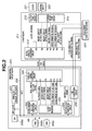
- Fig. 2 is a block diagram of a main control circuit board 201 of the image forming apparatus 100 and a driver board 211 of the image forming unit 50. Although a driver board 211 is provided in each of the four image forming units 50Y to 50K, Fig. 2 illustrates only one driver board 211 to simplify the description thereof.
- the driver board 211 is connected with a development high-voltage board 223 which applies an AC voltage to the development sleeve 4a in the image forming unit 50.
- the driver board 211 includes a clutch drive circuit 213 for driving a clutch 221 and a stepping motor drive circuit 214 for driving a stepping motor 222.
- the stepping motor 222 drives and rotates the development sleeve 4a in each of the four image forming units 50Y to 50K.
- the clutch 221 connects and disconnects a driving force transfer system between the stepping motor 222 and the development sleeve 4a.
- the main control circuit board 201 includes a central processing unit (CPU) 206a, a read-only memory (ROM) 206b, a random access memory (RAM) 206c, and an application specific integrated circuit (ASIC) 208.
- the CPU 206a controls the image forming apparatus 100 according to a program stored in the ROM 206b while using the RAM 206c as a work area.
- the CPU 206a, the ROM 206b, the RAM 206c, and the ASIC 208 are connected via a bus.
- the main control circuit board 201 outputs signals for controlling the development high-voltage board 223 which applies the development voltage to the developing unit 4.
- the signals for controlling the development high-voltage board 223 include a development DC ON signal, a development DC voltage control signal, a development AC ON signal, a development AC amplitude control signal, and a development AC clock signal (waveform signals for the developing unit 4). These signals are supplied to the development high-voltage board 223 via the driver board 211.
- a main clock oscillation circuit 207 generates a 12 MHz main clock signal (also referred to as reference clock signal) , and supplies the main clock signal to the CPU 206a and the ASIC 208.
- the ASIC 208 includes a development AC clock generation circuit 202, an output port register 203, a motor clock generation circuit 204, a parallel-to-serial conversion circuit 205, and a digital-to-analog (D/A) conversion circuit 209.
- the development AC clock generation circuit 202, the motor clock generation circuit 204, the parallel-to-serial conversion circuit 205, and the D/A conversion circuit 209 operate in synchronization with the main clock signal.
- Each of these circuits included in the ASIC 208 has a register used by the CPU 206a to set up a respective operation.
- the development AC clock generation circuit 202 divides the main clock signal, which is output from the main clock oscillation circuit 207, to generate the development AC clock signal according to a frequency and a duty ratio of the AC voltage, to be applied to the developing unit 4, set up by the CPU 206a.
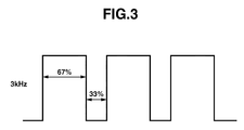
- the development AC clock signal is a rectangular wave clock signal as illustrated in Fig. 3 .
- the development AC clock signal has a frequency of 3 kHz and a duty ratio having 67% high-level width and 33% low-level width.
- the D/A conversion circuit 209 converts the development DC voltage control signal and the development AC amplitude control signal, which are digital signals, set by the CPU 206a into analog signals, and supplies the analog signals to the development high-voltage board 223 via the driver board 211.
- the output port register 203 controls various output ports according to a setting by the CPU 206a.
- the output port register 203 outputs the development DC ON signal, the development AC ON signal, a clutch ON signal, and motor current setting signals (a motor current setting 1 signal and a motor current setting 0 signal).
- the development DC ON signal and the development AC ON signal are used as an instruction to turn ON the output of the development AC voltage and the development DC voltage.
- the clutch ON signal is used as an instruction to turn ON the clutch 221.
- the motor current setting 1 signal and the motor current setting 0 signal set a drive current for the stepping motor 222.
- the motor clock generation circuit 204 divides the main clock signal, which is output from the main clock oscillation circuit 207, to generate a clock signal for driving the stepping motor 222.
- the stepping motor 222 rotates at a speed according to the set drive current and the generated clock signal.
- the parallel-to-serial conversion circuit 205 applies parallel-to-serial conversion to the signals input in parallel from the development AC clock generation circuit 202, the output port register 203, and the motor clock generation circuit 204 into serial form, and then transfers the converted signals to a serial-to-parallel conversion circuit 212 of the driver board 211.
- the parallel-to-serial conversion circuit 205 samples parallel signals at a predetermined period to convert them into serial signals.
- the serial-to-parallel conversion circuit 212 converts the serial signals transferred from the parallel-to-serial conversion circuit 205 into parallel signals.
- the main control circuit board 201 applies parallel-to-serial conversion to convert a plurality of parallel signals into serial form and then serially transmits the signals to the driver board 211 in this way, thus the number of the signal lines between the main control circuit board 201 and the driver board 211 can be reduced.
- This configuration not only contributes to downsizing of the image forming apparatus but also improves workability at the time of assembly operations of the image forming apparatus.
- This configuration is particularly effective for an image forming apparatus in which the main control circuit board 201, the driver board 211, and the development high-voltage board 223 are disposed separately.
- the parallel-to-serial conversion circuit 205 samples parallel signals at a frequency which is an integral multiple of the frequency of the development AC clock signal and converts the parallel signals into serial signals.
- the parallel-to-serial conversion circuit 205 samples the parallel signals at a frequency of 60 kHz which is 20 times the 3 kHz frequency of the development AC clock signal.
- the parallel-to-serial conversion circuit 205 performs parallel-to-serial conversion in synchronization with the main clock signal input from the main clock oscillation circuit 207 (so output by the main clock oscillation circuit).
- the parallel-to-serial conversion circuit 205 transmits a sampling signal XLOAD, a transfer clock signal SCK, and data SDATA to the serial-to-parallel conversion circuit 212.
- the sampling signal XLOAD is used to determine the timing of parallel-to-serial conversion and serial-to-parallel conversion.
- the transfer clock signal SCK is used to achieve synchronization in transferring parallel-to-serial-converted signals (serial signals) to the serial-to-parallel conversion circuit 212.
- the serial-to-parallel conversion circuit 212 receives the sampling signal XLOAD, the transfer clock signal SCK, and the data SDATA, and converts the data SDATA (serial signals) into parallel signals in synchronization with the transfer clock signal SCK.
- Fig. 4 illustrates signals assigned to input ports of the parallel-to-serial conversion circuit 205 and output ports of the serial-to-parallel conversion circuit 212.
- Input ports Pi7 to Pi1 of the parallel-to-serial conversion circuit 205 are assigned the clutch ON signal, the motor current setting 1 signal, the motor current setting 0 signal, the motor clock signal, the development DC ON signal, the development AC ON signal, and the development AC clock signal, respectively. These signals are connected to respective ports to be input from each circuit.
- Output ports Po7 to Po1 of the serial-to-parallel conversion circuit 212 are assigned the clutch ON signal, the motor current setting 1 signal, the motor current setting 0 signal, the motor clock signal, the development DC ON signal, the development AC ON signal, and the development AC clock signal, respectively. These signals are connected to respective ports to be output to each circuit.
- the clutch drive circuit 213 In response to the clutch ON signal input from the output port Po7, the clutch drive circuit 213 turns ON the clutch 221.
- the stepping motor drive circuit 214 supplies to the stepping motor 222 a drive current corresponding to the motor current setting 1 signal and the motor current setting 0 signal input from the output ports Po6 and Po5, respectively. Further, the stepping motor drive circuit 214 supplies the stepping motor 222 with the motor clock signal input from the output port Po4.
- the development high-voltage board 223 supplies the developing unit 4 with a DC voltage having a value specified by the development DC voltage control signal input from the D/A conversion circuit 209.
- the development high-voltage board 223 supplies the developing unit 4 with an AC voltage having an amplitude specified by the development AC amplitude control signal input from the D/A conversion circuit 209.
- the development high-voltage board 223 supplies the developing unit 4 with a voltage composed of a DC voltage and an AC voltage superimposed thereon when both the development DC ON signal and the development AC ON signal are ON.
- the development high-voltage board 223 supplies the developing unit 4 with a rectangular wave AC voltage having a period and duty ratio specified by the development AC clock signal input from the output port Po1 (so the development high-voltage board 223 is preferably arranged to supply the developing unit 4 with a voltage based on the serial signal SDATA transmitted by the parallel to serial conversion circuit 205).
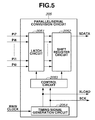
- Fig. 5 is a block diagram of the parallel-to-serial conversion circuit 205.
- Fig. 6 is a timing chart illustrating input and output signals for the parallel-to-serial conversion circuit 205.
- the parallel-to-serial conversion circuit 205 includes a latch circuit 2051, a shift register circuit 2052, a control circuit 2053, and a timing signal generation circuit 2054.
- the timing signal generation circuit 2054 generates a 1.2 MHz SCK signal formed by dividing the main clock signal into one-tenth (so by 10), and a sampling signal XLOAD for determining the timing of parallel-to-serial conversion and serial-to-parallel conversion.
- a falling edge of the sampling signal XLOAD specifies a sampling timing (so specifies a start time for starting sampling) for parallel-to-serial conversion.
- the timing signal generation circuit 2054 outputs the sampling signal XLOAD at a frequency of 60 kHz.
- Parallel signals Pi7 to Pi0 are input to the latch circuit 2051.
- the control circuit 2053 outputs a latch signal to the latch circuit 2051 on the falling edge of the sampling signal XLOAD.
- the latch circuit 2051 latches (retains) the input signals Pi7 to Pi0 and outputs the latched input signals Pi7 to Pi0 to the shift register circuit 2052.
- the control circuit 2053 outputs a shift signal to the shift register circuit 2052 on the falling edge of the transfer clock signal SCK.
- the shift register circuit 2052 sequentially selects the input signals Pi7 to Pi0 and outputs each signal as the data SDATA, in order of Pi7, Pi6, ..., Pi0.
- the parallel-to-serial conversion circuit 205 sequentially transmits the plurality of signals Pi7 to Pi0 to the serial-to-parallel conversion circuit 212 in synchronization with the transfer clock signal SCK.
- the parallel-to-serial conversion circuit 205 latches the plurality of signals on the falling edge of the sampling signal XLOAD, it may latch the signals on a rising edge of the sampling signal XLOAD.
- Fig. 7 is a block diagram of the serial-to-parallel conversion circuit 212.
- Fig. 8 is a timing chart illustrating input and output signals for the serial-to-parallel conversion circuit 212.
- the serial-to-parallel conversion circuit 212 includes a shift register circuit 2121, a latch circuit 2122, and a control circuit 2123. During a period in which the sampling signal XLOAD is set to the low level, the control circuit 2123 outputs the shift signal to the shift register circuit 2121 on each rising edge of the transfer clock signal SCK.
- the shift register circuit 2121 captures the signals Pi7, Pi6, ..., Pi0 sequentially input from the data SDATA as signals Po7, Po6, ... , Po0.
- the serial-to-parallel conversion circuit 212 sequentially receives the plurality of signals Pi7 to Pi0 from the parallel-to-serial conversion circuit 205 in synchronization with the transfer clock signal SCK.
- the sampling signal XLOAD is controlled so as to be set to the high level when the shift register circuit 2121 has captured all of the signals Po7 to Po0.
- the control circuit 2123 outputs a latch signal to the latch circuit 2122 on the rising edge of the sampling signal XLOAD.
- the latch circuit 2122 latches the signals Po7 to Po0 retained by the shift register circuit 2121.
- the signals latched by the latch circuit 2122 serve as output signals of the output ports Po7 to Po0 of the serial-to-parallel conversion circuit 212.
- serial-to-parallel conversion circuit 212 latches a plurality of signals on the rising edge of the sampling signal XLOAD
- the serial-to-parallel conversion circuit 212 may latch the signals on the falling edge of the sampling signal XLOAD.
- the parallel-to-serial conversion circuit 205 responds to the rising edge of the sampling signal XLOAD.
- Fig. 9 is a circuit diagram of the development high-voltage board 223.
- the D/A conversion circuit 209 on the main control circuit board 201 generates the development AC amplitude control signal and the development DC voltage control signal.
- the generated development AC amplitude control signal and development DC voltage control signal are input to the development high-voltage board 223.
- the output port register 203 generates the development AC ON signal and the development DC ON signal.
- the generated development AC ON signal and development DC ON signal are input to the development high-voltage board 223 via the parallel-to-serial conversion circuit 205 and the serial-to-parallel conversion circuit 212.
- the development AC clock generation circuit 202 generates the development AC clock signal.
- the generated development AC clock signal is input to the development high-voltage board 223 via the parallel-to-serial conversion circuit 205 and the serial-to-parallel conversion circuit 212.
- the development high-voltage board 223 includes a development DC high-voltage circuit 231 and a development AC high-voltage circuit 232. To the development DC high-voltage circuit 231, the development DC ON signal for turning ON its output and the development DC voltage control signal for setting its output voltage are input.
- the development AC high-voltage circuit 232 includes a development AC amplitude control circuit 234 and a development AC gate drive circuit 233.
- the development AC amplitude control circuit 234 applies a voltage corresponding to the development AC amplitude control signal to a bridge circuit 236 for driving the primary side of a development AC transformer 235, thus controlling the amplitude of the development AC high-voltage circuit 232.
- the development AC ON signal and the development AC clock signal are input to the development AC gate drive circuit 233.
- the development AC gate drive circuit 233 turns ON a gate 1 signal and turns OFF a gate 2 signal when both the development AC ON signal and the development AC clock signal are set to the high level. Further, the development AC gate drive circuit 233 turns OFF the gate 1 signal and turns ON the gate 2 signal when the development AC ON signal is set to the high level and the development AC clock signal is set to the low level. The development AC gate drive circuit 233 turns OFF both the gate 1 signal and the gate 2 signal while the development AC ON signal is set to the low level.
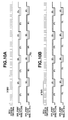
- Figs. 10A and 10B are timing charts illustrating a relation between a development AC clock signal Pi1 input to the parallel-to-serial conversion circuit 205 and a development AC clock signal Po1 output from the serial-to-parallel conversion circuit 212.
- the parallel-to-serial conversion circuit 205 converts the parallel signals Pi7 to Pi0 including the development AC clock signal Pi1 into serial signals at serial conversion timing of a predetermined frequency (corresponding to the frequency of the sampling signal XLOAD).
- the frequency of serial conversion timing is set to be an integral multiple of the frequency of the development AC clock signal. So the frequency of the XLOAD signal is set to be an integral multiple of frequency of the development AC clock signal.
- the sampling frequency of the parallel-to-serial conversion circuit 205 is set to 60 kHz which is 20 times the 3 kHz frequency of the development AC clock signal. The reason why the frequency of serial conversion timing is set to be an integral multiple of the frequency of the development AC clock signal will be described below with reference to Figs. 10A and 10B .
- Fig. 10A is a timing chart illustrating an example of a defect which occurs when the frequency of serial conversion timing is not an integral multiple of the frequency of the development AC clock signal.
- the frequency of the development AC clock signal is 3 kHz and the frequency of serial conversion timing is 50 kHz.
- the parallel-to-serial conversion circuit 205 samples parallel signals on the falling edge of the sampling signal XLOAD (so samples parallel signals between the falling edge and the next rising edge of the sampling signal XLOAD), and the serial-to-parallel conversion circuit 212 outputs parallel signals on the rising edge of the sampling signal XLOAD (so outputs parallel signals between the rising edge and the next falling edge of the sampling signal XLOAD).
- serial conversion timing corresponds to the falling edge of the sampling signal XLOAD.
- the development AC clock signal Pi1 does not synchronize with the serial conversion timing
- the development AC clock signal Po1 that has undergone serial conversion synchronizes with the serial conversion timing.
- the duty ratio of the development AC clock signal having 67% high-level width and 33% low-level width slightly changes to a duty ratio having 64% high-level width and 36% low-level width.
- this (consistent) change causes no problem since the contrast between charging potential and development potential is controlled by the image forming unit 50.
- a problem is that time variation in the duty ratio of the development AC clock signal Po1 changes the development density in the developing unit 4.
- the duty ratio of the development AC clock signal Po1 has 64% high-level width and 36% low-level width, jitter periodically occurs resulting in a duty ratio having 68% high-level width and 32% low-level width.
- a periodic band-like image density unevenness occurs in the rotational direction of the photosensitive drum 1, resulting in degraded image quality.
- a process speed of the image forming unit 50 is 400 mm/s
- an image density unevenness occurs at 1 mm pitch at a jitter frequency of 400 Hz or at 0.4 mm pitch at a jitter frequency of 1 kHz.
- the frequency of serial conversion timing of the parallel-to-serial conversion circuit 205 is set to be an integral multiple of the frequency of the development AC clock signal.
- Fig. 10B is a timing chart illustrating a preferable example in which the frequency of serial conversion timing is set to be an integral multiple of the frequency of the development AC clock signal.
- the frequency of the development AC clock signal is 3 kHz and the frequency of serial conversion timing is 60 kHz (so the frequency of the XLOAD signal is 60kHz) .
- the development AC clock signal Pi1 does not synchronize with the serial conversion timing
- the development AC clock signal Po1 that has undergone serial conversion synchronizes with the serial conversion timing.
- the duty ratio of the development AC clock signal having 67% high-level width and 33% low-level width slightly, but consistently, changes to a duty ratio having 70% high-level width and 30% low-level width.
- this change causes no problem since the contrast between charging potential and development potential is controlled by the image forming unit 50.
- the example in Fig. 10B differs from the example of defect in Fig. 10A in that there is no time variation (so no variation over time) in the duty ratio of the development AC clock signal Po1 at all since the frequency of serial conversion timing is set to be an integral multiple of the frequency of the development AC clock signal. Therefore, jitter due to above described parallel-to-serial conversion by the parallel-to-serial conversion circuit 205 does not occur in a signal corresponding to the development AC clock signal, thus an image density unevenness due to jitter can be prevented.
- the use of serial communication can reduce the number of signal lines while maintaining the image quality, thus cost reduction and space saving can be realized.
- the circuit for generating the development AC clock signal and the circuit for performing parallel-to-serial conversion by using the same reference clock like the present exemplary embodiment.
- the present exemplary embodiment is described based on a case where the development AC clock generation circuit 202, the output port register 203, the motor clock generation circuit 204, and the parallel-to-serial conversion circuit 205 are included in the ASIC 208, these circuits may be configured by separate integrated circuits (ICs).
- the present invention is also applicable to a case where an AC voltage is applied to the charging roller 2 as a second exemplary embodiment.
- a charging voltage composed of a DC voltage (for example, a predetermined DC voltage -300 to -900 VDC) and a sine wave AC voltage (a predetermined AC voltage 1300 to 2000 VAC) superimposed thereon is applied to the charging roller 2.
- a charging voltage composed of a DC voltage (for example, a predetermined DC voltage -300 to -900 VDC) and a sine wave AC voltage (a predetermined AC voltage 1300 to 2000 VAC) superimposed thereon is applied to the charging roller 2.
- a charging voltage composed of a DC voltage (for example, a predetermined DC voltage -300 to -900 VDC) and a sine wave AC voltage (a predetermined AC voltage 1300 to 2000 VAC) superimposed thereon is applied to the charging roller 2.
- an image forming apparatus according to the second exemplary embodiment is configured in a similar way to the image forming apparatus in the first exemplary embodiment.
- Fig. 11 is a block diagram of the main control circuit board 201 of the image forming apparatus 100 and the driver board 211 of the image forming unit 50.
- the configuration in Fig. 11 differs from the configuration in Fig. 2 in that an ASIC 308 on the main control circuit board 201 has a charging AC clock generation circuit 302 (instead of a development AC clock generation circuit 202) and a charging high-voltage board 323 (instead of a development high-voltage board 223) is connected to the driver board 211.
- the development-related signals in the first exemplary embodiment are replaced by charging-related signals in the second exemplary embodiment.
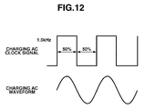
- the charging AC clock generation circuit 302 generates a charging AC clock signal (a waveform signal for charging devices) which is a rectangular wave clock signal as illustrated in Fig. 12 and has a frequency of 1.5 kHz and a duty ratio having 50% high-level width and 50% low-level width.
- a charging AC clock signal (a waveform signal for charging devices) which is a rectangular wave clock signal as illustrated in Fig. 12 and has a frequency of 1.5 kHz and a duty ratio having 50% high-level width and 50% low-level width.
- Fig. 13 is a circuit diagram of the charging high-voltage board 323.
- a D/A conversion circuit 206 arranged on the main control circuit board 201 generates a charging AC amplitude control signal and a charging DC voltage control signal.
- the generated charging AC amplitude control signal and charging DC voltage control signal are input into the charging high-voltage board 323.
- An output port register 303 generates a charging AC ON signal and a charging DC ON signal.
- the charging AC ON signal and the charging DC ON signal are input into the charging high-voltage board 323 via the parallel-to-serial conversion circuit 205 and the serial-to-parallel conversion circuit 212.
- the charging AC clock generation circuit 302 generates the charging AC clock signal.
- the generated charging AC clock signal is input into the charging high-voltage board 323 via the parallel-to-serial conversion circuit 205 and the serial-to-parallel circuit 212 (so the charging high-voltage board 323 is preferably arranged to supply the charging roller 2 with a voltage based on the serial signal SDATA transmitted by the parallel to serial conversion circuit 205).
- the charging high-voltage board 323 includes a charging DC high-voltage circuit 331 and a charging AC high-voltage circuit 332. To the charging DC high-voltage circuit 331, the charging DC ON signal for turning ON its output and the charging DC voltage control signal for setting up its output voltage are input.
- the charging AC high-voltage circuit 332 includes a charging AC amplitude control circuit 334, a low-pass filter 337, and an amplifier circuit 336.
- the charging AC amplitude control circuit 334 supplies a voltage corresponding to the charging AC amplitude control signal to a source of an field effect transistor (FET).
- FET field effect transistor
- the charging AC clock signal is input to a gate of the FET.
- a rectangular wave having the frequency of the charging AC clock signal is generated at a contact between the charging AC amplitude control circuit 334 and the FET.
- the low-pass filter 337 converts this rectangular wave into a sine wave.
- An output current of the low-pass filter 337 is amplified by the amplifier circuit 336 and then supplied to the charging roller 2 via a charging AC transformer 335.
- the frequency of serial conversion timing of the parallel-to-serial conversion circuit 205 is set to be an integral multiple of the frequency of the charging AC clock signal.
- the frequency of the charging AC clock signal is 1.5 kHz and the frequency of serial conversion timing is 60 kHz. Therefore, similar to the first exemplary embodiment, jitter due to above described parallel-to-serial conversion by the parallel-to-serial conversion circuit 205 does not occur in a signal corresponding to the charging AC clock signal, thus an image density unevenness due to jitter can be prevented.
- the present invention also provides a serial communication apparatus comprising: generation means configured to generate a waveform signal; and serial communication means configured to perform, at a predetermined sampling period, serial communication of the waveform signal generated by the generation means, wherein a frequency of the predetermined sampling period is an integral multiple of a frequency of the waveform signal.
- the present invention also provides an image forming apparatus including such a serial communication apparatus.
Landscapes
- Engineering & Computer Science (AREA)
- Theoretical Computer Science (AREA)
- Physics & Mathematics (AREA)
- General Physics & Mathematics (AREA)
- General Engineering & Computer Science (AREA)
- Control Or Security For Electrophotography (AREA)
- Developing For Electrophotography (AREA)
- Electrostatic Charge, Transfer And Separation In Electrography (AREA)
Abstract
Description
- The present invention relates to a serial communication apparatus which performs waveform signal serial communication and also to an image forming apparatus including the serial communication apparatus.
- It is known to use a development method, in an electrophotographic image forming apparatus, which forms an oscillating electric field between a photosensitive drum and a development sleeve of a developing unit to develop an electrostatic latent image on the photosensitive drum by a toner. The toner sufficiently adheres to image portions on the photosensitive drum by a biasing electric field of an oscillating electric field. The toner adhering to non-image portions on the photosensitive drum is separated therefrom by a back-biasing electric field of the oscillating electric field. To form the oscillating electric field, a development voltage composed of a direct-current (DC) voltage and an alternating-current (AC) voltage superimposed thereon is applied to the development sleeve. Japanese Patent Application Laid-Open No.
H4-356076 - The ratio of the biasing electric field to the back-biasing electric field can be easily controlled by applying a rectangular wave AC voltage to the development sleeve and controlling a duty ratio of high and low levels of the rectangular wave. More specifically, a main control circuit board generates a development AC clock signal representing a period and a duty ratio of the AC voltage applied to the development sleeve and a development AC amplitude control signal representing the amplitude of the AC voltage applied to the development sleeve. The main control circuit board transmits the development AC clock signal and the development AC amplitude control signal to a development high-voltage board. The development high-voltage board applies to the development sleeve the development voltage composed of a DC voltage and an AC voltage superimposed thereon, the AC voltage corresponding to the development AC clock signal and the development AC amplitude control signal.
- The main control circuit board of the image forming apparatus also transmits signals to a driver board which operates motors and clutches in the image forming apparatus. Signal lines for transmitting these signals connect the main control circuit board and the driver board and the main control circuit board and the development high-voltage board. With the increase in precision, in operation speed, and functional diversity of the image forming apparatus, the number of signal lines from the main control circuit board is also increasing. Since each circuit board is implemented apart (separate) from the main control circuit board in many cases, connecting the main control circuit board and each circuit board with a number of signal lines will not only make it difficult to downsize the image forming apparatus but also degrade the workability at the time of assembly operation of the image forming apparatus.
- This problem may possibly be solved by reducing the number of signal lines between the main control circuit board and each circuit board. In this case, the main control circuit board applies parallel-to-serial conversion to the above-described plurality of signals into serial form and then serially transmits the signals to each control circuit board. Then, each circuit board applies serial-to-parallel conversion to the received serial signals.
- However, transmitting the development AC clock signal having a constant duty ratio through parallel-to-serial conversion may cause time variation (jitter) in the duty ratio of the development AC clock signal after serial-to-parallel conversion because of a relation with a sampling period for parallel-to-serial conversion. If time variation in the duty ratio of the development AC clock signal appears, a band-like image density unevenness may occur along the rotational direction of the photosensitive drum.
- According to a first aspect of the present invention, there is provided a serial communication apparatus as specified in
claim 1. - According to a second aspect of the present invention, there is provided an image forming apparatus as specified in
claim 4. - According to a third aspect of the present invention, there is provided an image forming apparatus as specified in claim 5.
- Further features and aspects of the present invention will become apparent from the following detailed description of exemplary embodiments with reference to the attached drawings.
- The accompanying drawings, which are incorporated in and constitute a part of the specification, illustrate exemplary embodiments, features, and aspects of the invention and, together with the description, serve to explain the principles of the invention.
-
Fig. 1 is a sectional view of an image forming apparatus according to a first exemplary embodiment of the present invention. -
Fig. 2 is a block diagram of a main control circuit board and a driver board according to the first exemplary embodiment. -
Fig. 3 illustrates a development AC clock signal. -
Fig. 4 illustrates signals assigned to input ports of a parallel-to-serial conversion circuit and output ports of a serial-to-parallel conversion circuit. -
Fig. 5 is a block diagram of the parallel-to-serial conversion circuit. -
Fig. 6 is a timing chart illustrating input and output signals for the parallel-to-serial conversion circuit. -
Fig. 7 is a block diagram of the serial-to-parallel conversion circuit. -
Fig. 8 is a timing chart illustrating input and output signals for the serial-to-parallel conversion circuit. -
Fig. 9 is a circuit diagram of a development high-voltage board. -
Figs. 10A and 10B are timing charts illustrating a relation between the development AC clock signal input to the parallel-to-serial conversion circuit and the development AC clock signal output from the serial-to-parallel conversion circuit. -
Fig. 11 is a block diagram of a main control circuit board and a driver board according to a second exemplary embodiment. -
Fig. 12 illustrates a charging AC clock signal. -
Fig. 13 is a circuit diagram of the charging high-voltage board. - Various exemplary embodiments, features, and aspects of the invention will be described in detail below with reference to the drawings.
-
Fig. 1 is a sectional view of animage forming apparatus 100 according to a first exemplary embodiment of the present invention. Theimage forming apparatus 100 is an electrophotographic image forming apparatus which forms a color image using toner of four colors, namely yellow (Y), magenta (M), cyan (C), and black (K) toners. Theimage forming apparatus 100 includesimage forming units image forming units image forming units photosensitive drums charging rollers laser exposure units units primary transfer rollers image forming units - The
charging roller 2 is provided in contact with thephotosensitive drum 1, and driven and rotated by the rotation of thephotosensitive drum 1. A DC voltage (for example, a predetermined DC voltage -1000 to -1500 VDC) is applied to thecharging roller 2 as a charging voltage. A surface of thephotosensitive drum 1 is uniformly charged to a predetermined (negative) potential by thecharging roller 2. The charging voltage may be applied to thephotosensitive drum 1 by a charging member other than thecharging roller 2. Further, as long as electric discharge for applying the charging voltage is performed between the charging member and thephotosensitive drum 1, a micro gap (for example, about 10 micrometers) may be provided between the charging member and thephotosensitive drum 1. - The laser exposure unit 3 modulates laser light based on an image signal. The laser light modulated by the laser exposure unit 3 is deflected in a main scanning direction, and then applied onto the rotating photosensitive drum 1 (photosensitive member). Performing the exposure process corresponding to an image in this way forms an electrostatic latent image on the
photosensitive drum 1. - The developing
unit 4 supplies the toner to thephotosensitive drum 1 via arotating development sleeve 4a. The development voltage composed of a predetermined DC voltage -150 to -700 VDC and a predetermined AC voltage 1000 to 2000 VAC superimposed thereon is applied to thedevelopment sleeve 4a. Thus, negatively charged toner is supplied to thephotosensitive drum 1, and the electrostatic latent image formed on thephotosensitive drum 1 is developed by the toner. - The primary transfer roller 5 is driven and rotated by the movement of an
intermediate transfer belt 6. A DC voltage having a potential (positive potential) opposite to the potential of the toner is applied to the primary transfer roller 5 as a primary transfer voltage. Thus, the toner image formed on thephotosensitive drum 1 is transferred onto theintermediate transfer belt 6. - Toner images of respective colors formed by the four
image forming units 50Y to 50K are superimposed one another and transferred onto the intermediate transfer belt 6 (primary transfer process). Thus, a full color toner image is formed and borne on theintermediate transfer belt 6. The full color toner image borne on theintermediate transfer belt 6 is transferred by asecondary transfer roller 8 onto a sheet P which is fed from asheet cassette 10 and conveyed into a gap between thesecondary transfer roller 8 and the intermediate transfer belt 6 (secondary transfer process). A predetermined DC voltage +500 to +7000 VDC is applied to thesecondary transfer roller 8. - The sheet P having the full color toner image transferred thereon is conveyed to a fixing
device 11. The fixingdevice 11 applies heat and pressure to the sheet P to fix the toner image thereon. The sheet P having the toner image fixed thereon passes through aconveyance path 12 and adelivery roller 13, and then is discharged onto adischarge tray 14. -
Fig. 2 is a block diagram of a maincontrol circuit board 201 of theimage forming apparatus 100 and adriver board 211 of theimage forming unit 50. Although adriver board 211 is provided in each of the fourimage forming units 50Y to 50K,Fig. 2 illustrates only onedriver board 211 to simplify the description thereof. - The
driver board 211 is connected with a development high-voltage board 223 which applies an AC voltage to thedevelopment sleeve 4a in theimage forming unit 50. Thedriver board 211 includes aclutch drive circuit 213 for driving a clutch 221 and a steppingmotor drive circuit 214 for driving a steppingmotor 222. The steppingmotor 222 drives and rotates thedevelopment sleeve 4a in each of the fourimage forming units 50Y to 50K. The clutch 221 connects and disconnects a driving force transfer system between the steppingmotor 222 and thedevelopment sleeve 4a. - The main
control circuit board 201 includes a central processing unit (CPU) 206a, a read-only memory (ROM) 206b, a random access memory (RAM) 206c, and an application specific integrated circuit (ASIC) 208. TheCPU 206a controls theimage forming apparatus 100 according to a program stored in theROM 206b while using theRAM 206c as a work area. TheCPU 206a, theROM 206b, theRAM 206c, and theASIC 208 are connected via a bus. - The main
control circuit board 201 outputs signals for controlling the development high-voltage board 223 which applies the development voltage to the developingunit 4. The signals for controlling the development high-voltage board 223 include a development DC ON signal, a development DC voltage control signal, a development AC ON signal, a development AC amplitude control signal, and a development AC clock signal (waveform signals for the developing unit 4). These signals are supplied to the development high-voltage board 223 via thedriver board 211. - A main
clock oscillation circuit 207 generates a 12 MHz main clock signal (also referred to as reference clock signal) , and supplies the main clock signal to theCPU 206a and theASIC 208. TheASIC 208 includes a development ACclock generation circuit 202, anoutput port register 203, a motorclock generation circuit 204, a parallel-to-serial conversion circuit 205, and a digital-to-analog (D/A)conversion circuit 209. The development ACclock generation circuit 202, the motorclock generation circuit 204, the parallel-to-serial conversion circuit 205, and the D/A conversion circuit 209 operate in synchronization with the main clock signal. Each of these circuits included in theASIC 208 has a register used by theCPU 206a to set up a respective operation. - The development AC
clock generation circuit 202 divides the main clock signal, which is output from the mainclock oscillation circuit 207, to generate the development AC clock signal according to a frequency and a duty ratio of the AC voltage, to be applied to the developingunit 4, set up by theCPU 206a. The development AC clock signal is a rectangular wave clock signal as illustrated inFig. 3 . In the present exemplary embodiment, the development AC clock signal has a frequency of 3 kHz and a duty ratio having 67% high-level width and 33% low-level width. - The D/
A conversion circuit 209 converts the development DC voltage control signal and the development AC amplitude control signal, which are digital signals, set by theCPU 206a into analog signals, and supplies the analog signals to the development high-voltage board 223 via thedriver board 211. - The
output port register 203 controls various output ports according to a setting by theCPU 206a. Theoutput port register 203 outputs the development DC ON signal, the development AC ON signal, a clutch ON signal, and motor current setting signals (a motor current setting 1 signal and a motor current setting 0 signal). - The development DC ON signal and the development AC ON signal are used as an instruction to turn ON the output of the development AC voltage and the development DC voltage. The clutch ON signal is used as an instruction to turn ON the clutch 221. The motor current setting 1 signal and the motor current setting 0 signal set a drive current for the stepping
motor 222. The motorclock generation circuit 204 divides the main clock signal, which is output from the mainclock oscillation circuit 207, to generate a clock signal for driving the steppingmotor 222. The steppingmotor 222 rotates at a speed according to the set drive current and the generated clock signal. - The parallel-to-
serial conversion circuit 205 applies parallel-to-serial conversion to the signals input in parallel from the development ACclock generation circuit 202, theoutput port register 203, and the motorclock generation circuit 204 into serial form, and then transfers the converted signals to a serial-to-parallel conversion circuit 212 of thedriver board 211. The parallel-to-serial conversion circuit 205 samples parallel signals at a predetermined period to convert them into serial signals. The serial-to-parallel conversion circuit 212 converts the serial signals transferred from the parallel-to-serial conversion circuit 205 into parallel signals. - The main
control circuit board 201 applies parallel-to-serial conversion to convert a plurality of parallel signals into serial form and then serially transmits the signals to thedriver board 211 in this way, thus the number of the signal lines between the maincontrol circuit board 201 and thedriver board 211 can be reduced. This configuration not only contributes to downsizing of the image forming apparatus but also improves workability at the time of assembly operations of the image forming apparatus. This configuration is particularly effective for an image forming apparatus in which the maincontrol circuit board 201, thedriver board 211, and the development high-voltage board 223 are disposed separately. - The parallel-to-
serial conversion circuit 205 samples parallel signals at a frequency which is an integral multiple of the frequency of the development AC clock signal and converts the parallel signals into serial signals. In the present exemplary embodiment, the parallel-to-serial conversion circuit 205 samples the parallel signals at a frequency of 60 kHz which is 20 times the 3 kHz frequency of the development AC clock signal. - The parallel-to-
serial conversion circuit 205 performs parallel-to-serial conversion in synchronization with the main clock signal input from the main clock oscillation circuit 207 (so output by the main clock oscillation circuit). The parallel-to-serial conversion circuit 205 transmits a sampling signal XLOAD, a transfer clock signal SCK, and data SDATA to the serial-to-parallel conversion circuit 212. - The sampling signal XLOAD is used to determine the timing of parallel-to-serial conversion and serial-to-parallel conversion. The transfer clock signal SCK is used to achieve synchronization in transferring parallel-to-serial-converted signals (serial signals) to the serial-to-
parallel conversion circuit 212. - The serial-to-
parallel conversion circuit 212 receives the sampling signal XLOAD, the transfer clock signal SCK, and the data SDATA, and converts the data SDATA (serial signals) into parallel signals in synchronization with the transfer clock signal SCK. -
Fig. 4 illustrates signals assigned to input ports of the parallel-to-serial conversion circuit 205 and output ports of the serial-to-parallel conversion circuit 212. Input ports Pi7 to Pi1 of the parallel-to-serial conversion circuit 205 are assigned the clutch ON signal, the motor current setting 1 signal, the motor current setting 0 signal, the motor clock signal, the development DC ON signal, the development AC ON signal, and the development AC clock signal, respectively. These signals are connected to respective ports to be input from each circuit. - Output ports Po7 to Po1 of the serial-to-
parallel conversion circuit 212 are assigned the clutch ON signal, the motor current setting 1 signal, the motor current setting 0 signal, the motor clock signal, the development DC ON signal, the development AC ON signal, and the development AC clock signal, respectively. These signals are connected to respective ports to be output to each circuit. - In response to the clutch ON signal input from the output port Po7, the
clutch drive circuit 213 turns ON the clutch 221. The steppingmotor drive circuit 214 supplies to the stepping motor 222 a drive current corresponding to the motor current setting 1 signal and the motor current setting 0 signal input from the output ports Po6 and Po5, respectively. Further, the steppingmotor drive circuit 214 supplies the steppingmotor 222 with the motor clock signal input from the output port Po4. - During a period responding to the development DC ON signal input from the output port Po3 (so during the time period that the ON signal is in the ON state), the development high-
voltage board 223 supplies the developingunit 4 with a DC voltage having a value specified by the development DC voltage control signal input from the D/A conversion circuit 209. During a period responding to the development AC ON signal input from the output port Po2 (so during the time period that the ON signal is in the ON state) , the development high-voltage board 223 supplies the developingunit 4 with an AC voltage having an amplitude specified by the development AC amplitude control signal input from the D/A conversion circuit 209. The development high-voltage board 223 supplies the developingunit 4 with a voltage composed of a DC voltage and an AC voltage superimposed thereon when both the development DC ON signal and the development AC ON signal are ON. The development high-voltage board 223 supplies the developingunit 4 with a rectangular wave AC voltage having a period and duty ratio specified by the development AC clock signal input from the output port Po1 (so the development high-voltage board 223 is preferably arranged to supply the developingunit 4 with a voltage based on the serial signal SDATA transmitted by the parallel to serial conversion circuit 205). -
Fig. 5 is a block diagram of the parallel-to-serial conversion circuit 205.Fig. 6 is a timing chart illustrating input and output signals for the parallel-to-serial conversion circuit 205. The parallel-to-serial conversion circuit 205 includes alatch circuit 2051, ashift register circuit 2052, acontrol circuit 2053, and a timingsignal generation circuit 2054. The timingsignal generation circuit 2054 generates a 1.2 MHz SCK signal formed by dividing the main clock signal into one-tenth (so by 10), and a sampling signal XLOAD for determining the timing of parallel-to-serial conversion and serial-to-parallel conversion. - As illustrated in
Fig. 6 , a falling edge of the sampling signal XLOAD specifies a sampling timing (so specifies a start time for starting sampling) for parallel-to-serial conversion. The timingsignal generation circuit 2054 outputs the sampling signal XLOAD at a frequency of 60 kHz. Parallel signals Pi7 to Pi0 are input to thelatch circuit 2051. - The
control circuit 2053 outputs a latch signal to thelatch circuit 2051 on the falling edge of the sampling signal XLOAD. In response to the latch signal, thelatch circuit 2051 latches (retains) the input signals Pi7 to Pi0 and outputs the latched input signals Pi7 to Pi0 to theshift register circuit 2052. During a period in which the sampling signal XLOAD is set to the low level, thecontrol circuit 2053 outputs a shift signal to theshift register circuit 2052 on the falling edge of the transfer clock signal SCK. - In response to the shift signal, the
shift register circuit 2052 sequentially selects the input signals Pi7 to Pi0 and outputs each signal as the data SDATA, in order of Pi7, Pi6, ..., Pi0. Thus, the parallel-to-serial conversion circuit 205 sequentially transmits the plurality of signals Pi7 to Pi0 to the serial-to-parallel conversion circuit 212 in synchronization with the transfer clock signal SCK. Although the parallel-to-serial conversion circuit 205 latches the plurality of signals on the falling edge of the sampling signal XLOAD, it may latch the signals on a rising edge of the sampling signal XLOAD. -
Fig. 7 is a block diagram of the serial-to-parallel conversion circuit 212.Fig. 8 is a timing chart illustrating input and output signals for the serial-to-parallel conversion circuit 212. The serial-to-parallel conversion circuit 212 includes ashift register circuit 2121, alatch circuit 2122, and acontrol circuit 2123. During a period in which the sampling signal XLOAD is set to the low level, thecontrol circuit 2123 outputs the shift signal to theshift register circuit 2121 on each rising edge of the transfer clock signal SCK. - In response to the shift signal, the
shift register circuit 2121 captures the signals Pi7, Pi6, ..., Pi0 sequentially input from the data SDATA as signals Po7, Po6, ... , Po0. Thus, the serial-to-parallel conversion circuit 212 sequentially receives the plurality of signals Pi7 to Pi0 from the parallel-to-serial conversion circuit 205 in synchronization with the transfer clock signal SCK. The sampling signal XLOAD is controlled so as to be set to the high level when theshift register circuit 2121 has captured all of the signals Po7 to Po0. - The
control circuit 2123 outputs a latch signal to thelatch circuit 2122 on the rising edge of the sampling signal XLOAD. In response to the latch signal, thelatch circuit 2122 latches the signals Po7 to Po0 retained by theshift register circuit 2121. The signals latched by thelatch circuit 2122 serve as output signals of the output ports Po7 to Po0 of the serial-to-parallel conversion circuit 212. - Although the serial-to-
parallel conversion circuit 212 latches a plurality of signals on the rising edge of the sampling signal XLOAD, the serial-to-parallel conversion circuit 212 may latch the signals on the falling edge of the sampling signal XLOAD. In this case, the parallel-to-serial conversion circuit 205 responds to the rising edge of the sampling signal XLOAD. -
Fig. 9 is a circuit diagram of the development high-voltage board 223. The D/A conversion circuit 209 on the maincontrol circuit board 201 generates the development AC amplitude control signal and the development DC voltage control signal. The generated development AC amplitude control signal and development DC voltage control signal are input to the development high-voltage board 223. Theoutput port register 203 generates the development AC ON signal and the development DC ON signal. The generated development AC ON signal and development DC ON signal are input to the development high-voltage board 223 via the parallel-to-serial conversion circuit 205 and the serial-to-parallel conversion circuit 212. The development ACclock generation circuit 202 generates the development AC clock signal. The generated development AC clock signal is input to the development high-voltage board 223 via the parallel-to-serial conversion circuit 205 and the serial-to-parallel conversion circuit 212. - The development high-
voltage board 223 includes a development DC high-voltage circuit 231 and a development AC high-voltage circuit 232. To the development DC high-voltage circuit 231, the development DC ON signal for turning ON its output and the development DC voltage control signal for setting its output voltage are input. The development AC high-voltage circuit 232 includes a development ACamplitude control circuit 234 and a development ACgate drive circuit 233. - The development AC
amplitude control circuit 234 applies a voltage corresponding to the development AC amplitude control signal to abridge circuit 236 for driving the primary side of adevelopment AC transformer 235, thus controlling the amplitude of the development AC high-voltage circuit 232. The development AC ON signal and the development AC clock signal are input to the development ACgate drive circuit 233. - The development AC
gate drive circuit 233 turns ON agate 1 signal and turns OFF agate 2 signal when both the development AC ON signal and the development AC clock signal are set to the high level. Further, the development ACgate drive circuit 233 turns OFF thegate 1 signal and turns ON thegate 2 signal when the development AC ON signal is set to the high level and the development AC clock signal is set to the low level. The development ACgate drive circuit 233 turns OFF both thegate 1 signal and thegate 2 signal while the development AC ON signal is set to the low level. -
Figs. 10A and 10B are timing charts illustrating a relation between a development AC clock signal Pi1 input to the parallel-to-serial conversion circuit 205 and a development AC clock signal Po1 output from the serial-to-parallel conversion circuit 212. The parallel-to-serial conversion circuit 205 converts the parallel signals Pi7 to Pi0 including the development AC clock signal Pi1 into serial signals at serial conversion timing of a predetermined frequency (corresponding to the frequency of the sampling signal XLOAD). - The frequency of serial conversion timing is set to be an integral multiple of the frequency of the development AC clock signal. So the frequency of the XLOAD signal is set to be an integral multiple of frequency of the development AC clock signal. In the present exemplary embodiment, the sampling frequency of the parallel-to-
serial conversion circuit 205 is set to 60 kHz which is 20 times the 3 kHz frequency of the development AC clock signal. The reason why the frequency of serial conversion timing is set to be an integral multiple of the frequency of the development AC clock signal will be described below with reference toFigs. 10A and 10B . -
Fig. 10A is a timing chart illustrating an example of a defect which occurs when the frequency of serial conversion timing is not an integral multiple of the frequency of the development AC clock signal. In the example inFig. 10A , the frequency of the development AC clock signal is 3 kHz and the frequency of serial conversion timing is 50 kHz. As described above, the parallel-to-serial conversion circuit 205 samples parallel signals on the falling edge of the sampling signal XLOAD (so samples parallel signals between the falling edge and the next rising edge of the sampling signal XLOAD), and the serial-to-parallel conversion circuit 212 outputs parallel signals on the rising edge of the sampling signal XLOAD (so outputs parallel signals between the rising edge and the next falling edge of the sampling signal XLOAD). - Referring to
Fig. 10A , serial conversion timing corresponds to the falling edge of the sampling signal XLOAD. As illustrated inFig. 10A , although the development AC clock signal Pi1 does not synchronize with the serial conversion timing, the development AC clock signal Po1 that has undergone serial conversion synchronizes with the serial conversion timing. Accordingly, the duty ratio of the development AC clock signal having 67% high-level width and 33% low-level width slightly changes to a duty ratio having 64% high-level width and 36% low-level width. However, this (consistent) change causes no problem since the contrast between charging potential and development potential is controlled by theimage forming unit 50. - In the example in
Fig. 10A , a problem is that time variation in the duty ratio of the development AC clock signal Po1 changes the development density in the developingunit 4. Referring toFig. 10A , although, most of the time, the duty ratio of the development AC clock signal Po1 has 64% high-level width and 36% low-level width, jitter periodically occurs resulting in a duty ratio having 68% high-level width and 32% low-level width. - When the period of the jitter is visible, a periodic band-like image density unevenness (banding) occurs in the rotational direction of the
photosensitive drum 1, resulting in degraded image quality. For example, when a process speed of theimage forming unit 50 is 400 mm/s, an image density unevenness occurs at 1 mm pitch at a jitter frequency of 400 Hz or at 0.4 mm pitch at a jitter frequency of 1 kHz. - In order to prevent the jitter causing such image density unevenness, in the present exemplary embodiment, the frequency of serial conversion timing of the parallel-to-
serial conversion circuit 205 is set to be an integral multiple of the frequency of the development AC clock signal.Fig. 10B is a timing chart illustrating a preferable example in which the frequency of serial conversion timing is set to be an integral multiple of the frequency of the development AC clock signal. In the example inFig. 10B , the frequency of the development AC clock signal is 3 kHz and the frequency of serial conversion timing is 60 kHz (so the frequency of the XLOAD signal is 60kHz) . - As illustrated in
Fig. 10B , although the development AC clock signal Pi1 does not synchronize with the serial conversion timing, the development AC clock signal Po1 that has undergone serial conversion synchronizes with the serial conversion timing. Accordingly, the duty ratio of the development AC clock signal having 67% high-level width and 33% low-level width slightly, but consistently, changes to a duty ratio having 70% high-level width and 30% low-level width. However, this change causes no problem since the contrast between charging potential and development potential is controlled by theimage forming unit 50. - The example in
Fig. 10B differs from the example of defect inFig. 10A in that there is no time variation (so no variation over time) in the duty ratio of the development AC clock signal Po1 at all since the frequency of serial conversion timing is set to be an integral multiple of the frequency of the development AC clock signal. Therefore, jitter due to above described parallel-to-serial conversion by the parallel-to-serial conversion circuit 205 does not occur in a signal corresponding to the development AC clock signal, thus an image density unevenness due to jitter can be prevented. The use of serial communication can reduce the number of signal lines while maintaining the image quality, thus cost reduction and space saving can be realized. - To reliably obtain the above described effect, it is desirable to operate the circuit for generating the development AC clock signal and the circuit for performing parallel-to-serial conversion by using the same reference clock, like the present exemplary embodiment. Although the present exemplary embodiment is described based on a case where the development AC
clock generation circuit 202, theoutput port register 203, the motorclock generation circuit 204, and the parallel-to-serial conversion circuit 205 are included in theASIC 208, these circuits may be configured by separate integrated circuits (ICs). - Although the first exemplary embodiment is described based on a case where an AC voltage is applied to the developing
unit 4, the present invention is also applicable to a case where an AC voltage is applied to the chargingroller 2 as a second exemplary embodiment. In the second exemplary embodiment, a charging voltage composed of a DC voltage (for example, a predetermined DC voltage -300 to -900 VDC) and a sine wave AC voltage (a predetermined AC voltage 1300 to 2000 VAC) superimposed thereon is applied to the chargingroller 2. Except for an AC charging configuration, an image forming apparatus according to the second exemplary embodiment is configured in a similar way to the image forming apparatus in the first exemplary embodiment. -
Fig. 11 is a block diagram of the maincontrol circuit board 201 of theimage forming apparatus 100 and thedriver board 211 of theimage forming unit 50. The configuration inFig. 11 differs from the configuration inFig. 2 in that anASIC 308 on the maincontrol circuit board 201 has a charging AC clock generation circuit 302 (instead of a development AC clock generation circuit 202) and a charging high-voltage board 323 (instead of a development high-voltage board 223) is connected to thedriver board 211. Further, the development-related signals in the first exemplary embodiment are replaced by charging-related signals in the second exemplary embodiment. The charging ACclock generation circuit 302 generates a charging AC clock signal (a waveform signal for charging devices) which is a rectangular wave clock signal as illustrated inFig. 12 and has a frequency of 1.5 kHz and a duty ratio having 50% high-level width and 50% low-level width. -
Fig. 13 is a circuit diagram of the charging high-voltage board 323. A D/A conversion circuit 206 arranged on the maincontrol circuit board 201 generates a charging AC amplitude control signal and a charging DC voltage control signal. The generated charging AC amplitude control signal and charging DC voltage control signal are input into the charging high-voltage board 323. An output port register 303 generates a charging AC ON signal and a charging DC ON signal. The charging AC ON signal and the charging DC ON signal are input into the charging high-voltage board 323 via the parallel-to-serial conversion circuit 205 and the serial-to-parallel conversion circuit 212. The charging ACclock generation circuit 302 generates the charging AC clock signal. The generated charging AC clock signal is input into the charging high-voltage board 323 via the parallel-to-serial conversion circuit 205 and the serial-to-parallel circuit 212 (so the charging high-voltage board 323 is preferably arranged to supply the chargingroller 2 with a voltage based on the serial signal SDATA transmitted by the parallel to serial conversion circuit 205). - The charging high-
voltage board 323 includes a charging DC high-voltage circuit 331 and a charging AC high-voltage circuit 332. To the charging DC high-voltage circuit 331, the charging DC ON signal for turning ON its output and the charging DC voltage control signal for setting up its output voltage are input. The charging AC high-voltage circuit 332 includes a charging ACamplitude control circuit 334, a low-pass filter 337, and anamplifier circuit 336. - During a period in which the charging AC ON signal is ON, the charging AC
amplitude control circuit 334 supplies a voltage corresponding to the charging AC amplitude control signal to a source of an field effect transistor (FET). The charging AC clock signal is input to a gate of the FET. Thus, a rectangular wave having the frequency of the charging AC clock signal is generated at a contact between the charging ACamplitude control circuit 334 and the FET. The low-pass filter 337 converts this rectangular wave into a sine wave. An output current of the low-pass filter 337 is amplified by theamplifier circuit 336 and then supplied to the chargingroller 2 via a charging AC transformer 335. - In the present exemplary embodiment, the frequency of serial conversion timing of the parallel-to-
serial conversion circuit 205 is set to be an integral multiple of the frequency of the charging AC clock signal. In the present exemplary embodiment, the frequency of the charging AC clock signal is 1.5 kHz and the frequency of serial conversion timing is 60 kHz. Therefore, similar to the first exemplary embodiment, jitter due to above described parallel-to-serial conversion by the parallel-to-serial conversion circuit 205 does not occur in a signal corresponding to the charging AC clock signal, thus an image density unevenness due to jitter can be prevented. - The present invention also provides a serial communication apparatus comprising: generation means configured to generate a waveform signal; and serial communication means configured to perform, at a predetermined sampling period, serial communication of the waveform signal generated by the generation means, wherein a frequency of the predetermined sampling period is an integral multiple of a frequency of the waveform signal. The present invention also provides an image forming apparatus including such a serial communication apparatus.
- While the present invention has been described with reference to exemplary embodiments, it is to be understood that the invention is not limited to the disclosed exemplary embodiments. The scope of the following claims is to be accorded the broadest interpretation so as to encompass all modifications, equivalent structures, and functions.
Claims (12)
- A serial communication apparatus (201) comprising:generation means (202, 302) configured to generate a waveform signal having a frequency; andserial communication means (205) configured to sample, at a predetermined sampling frequency, the waveform signal generated by the generation means and to transmit the results of the sampling as a serial signal (SDATA),wherein the predetermined sampling frequency is an integral multiple of the frequency of the waveform signal.
- The serial communication apparatus according to claim 1, wherein the serial communication means comprises a parallel-to-serial conversion means (205) configured to apply parallel-to-serial conversion to a plurality of signals including the waveform signal generated by the generation means by sampling the plurality of signals at the predetermined sampling frequency.
- The serial communication apparatus according to claim 2, comprising
a serial-to-parallel conversion means (212) configured to apply, at the predetermined sampling frequency, serial-to-parallel conversion to the serial signal transmitted by the parallel-to-serial conversion means. - An image forming apparatus including the serial communication apparatus according to any preceding claim, the image forming apparatus comprising:a photosensitive member (1);exposure means (3) configured to expose the photosensitive member in accordance with an image signal;developing means (4) configured to develop, using a toner, an electrostatic latent image formed on the photosensitive member exposed by the exposure means; andvoltage applying means (223) configured to apply to the developing means a voltage based on the result of sampling corresponding to the waveform signal transmitted from the serial communication means.
- An image forming apparatus including the serial communication apparatus according to any of claims 1 to 3, the image forming apparatus comprising:a photosensitive member (1);charging means (2) configured to charge the photosensitive member;exposure means (3) configured to expose the photosensitive member in accordance with an image signal;developing means (4) configured to develop, using a toner, an electrostatic latent image formed on the photosensitive member exposed by the exposure means; andvoltage applying means (323) configured to apply to the charging means a voltage based on the result of sampling corresponding to the waveform signal transmitted from the serial communication means.
- The image forming apparatus according to claim 4 when dependent on claim 2 or claim 5 when dependent on claim 2, further comprising oscillation means (207) configured to generate a reference clock signal and supply the reference clock signal to the generation means and the parallel-to-serial conversion means,
wherein the generation means and the parallel-to-serial conversion means are configured to operate in synchronization with the reference clock signal generated by the oscillation means. - The image forming apparatus according to claim 4 when dependent on claim 3,
wherein the parallel-to-serial conversion means is configured to apply parallel-to-serial conversion to a plurality of signals including a voltage ON signal and the waveform signal which are input to the voltage applying means,
wherein the serial-to-parallel conversion means is configured to apply serial-to-parallel conversion to the signals output from the parallel-to-serial conversion means, and to supply a signal corresponding to the voltage ON signal to the voltage applying means, and
wherein, during a period responding to the signal corresponding to the voltage ON signal, the voltage applying means is configured to apply a voltage corresponding to the waveform signal to the developing means. - The image forming apparatus according to claim 5 when dependent on claim 3,
wherein the parallel-to-serial conversion means is configured to apply parallel-to-serial conversion to a plurality of signals including a voltage ON signal and the waveform signal which are input to the voltage applying means,
wherein the serial-to-parallel conversion means is configured to apply serial-to-parallel conversion to the signals output from the parallel-to-serial conversion means, and to supply a signal corresponding to the voltage ON signal to the voltage applying means, and
wherein, during a period responding to the signal corresponding to the voltage ON signal, the voltage applying means is configured to apply a voltage corresponding to the waveform signal to the charging means. - The image forming apparatus according to claim 4 when dependent on claim 3 or according to claim 5 when dependent on claim 3, further comprising motor drive means (214) configured to drive a stepping motor,
wherein the parallel-to-serial conversion means is configured to apply parallel-to-serial conversion to a plurality of signals including a motor current setting signal or a motor clock signal and the waveform signal which are input to the motor drive means,
wherein the serial-to-parallel conversion means is configured to apply serial-to-parallel conversion to the signals output from the parallel-to-serial conversion means, and supplies a signal corresponding to the motor current setting signal or the motor clock signal to the motor drive means, and
wherein the motor drive means supplies to the stepping motor a current or a clock signal according to the signal corresponding to the motor current setting signal or the motor clock signal. - The image forming apparatus according to claim 4 when dependent on claim 3 or according to claim 5 when dependent on claim 3, further comprising clutch drive means (213) configured to drive a clutch,
wherein the parallel-to-serial conversion means is configured to apply parallel-to-serial conversion to a plurality of signals including a clutch ON signal and the waveform signal which are input to the clutch drive means,
wherein the serial-to-parallel conversion means is configured to apply serial-to-parallel conversion to the signals output from the parallel-to-serial conversion means, and to supply a signal corresponding to the clutch ON signal to the clutch drive means, and
wherein the clutch drive means is configured to turn ON the clutch in response to the signal corresponding to the clutch ON signal. - The image forming apparatus according to claim 4 when dependent on claim 3 or according to claim 5 when dependent on claim 3, wherein the parallel-to-serial conversion means is configured to generate a sampling signal (XLOAD) for determining a sampling timing for parallel-to-serial conversion and a transfer clock signal (SCK) for achieving synchronization in transferring a parallel-to-serial converted signal to the serial-to-parallel conversion means, to latch the plurality of signals at a timing corresponding to a falling edge or a rising edge of the sampling signal, and to sequentially transmit the plurality of signals (SDATA) to the serial-to-parallel conversion means in synchronization with the transfer clock signal.
- The image forming apparatus according to claim 11,
wherein the parallel-to-serial conversion means is configured to transmit the sampling signal, the transfer clock signal, and the plurality of signals to the serial-to-parallel conversion means via different signal lines, and
wherein the serial-to-parallel conversion means is configured to sequentially receive the plurality of signals in synchronization with the transfer clock signal, and to latch the plurality of signals at a timing corresponding to a rising edge or a falling edge of the sampling signal.
Applications Claiming Priority (1)
| Application Number | Priority Date | Filing Date | Title |
|---|---|---|---|
| JP2010052021A JP5038449B2 (en) | 2010-03-09 | 2010-03-09 | Image forming apparatus |
Publications (3)
| Publication Number | Publication Date |
|---|---|
| EP2365631A2 true EP2365631A2 (en) | 2011-09-14 |
| EP2365631A3 EP2365631A3 (en) | 2012-02-01 |
| EP2365631B1 EP2365631B1 (en) | 2013-11-20 |
Family
ID=44247489
Family Applications (1)
| Application Number | Title | Priority Date | Filing Date |
|---|---|---|---|
| EP11155612.2A Not-in-force EP2365631B1 (en) | 2010-03-09 | 2011-02-23 | Serial communication apparatus and image forming apparatus including the same |
Country Status (5)
| Country | Link |
|---|---|
| US (1) | US8577243B2 (en) |
| EP (1) | EP2365631B1 (en) |
| JP (1) | JP5038449B2 (en) |
| KR (1) | KR101324394B1 (en) |
| CN (1) | CN102193405B (en) |
Cited By (1)
| Publication number | Priority date | Publication date | Assignee | Title |
|---|---|---|---|---|
| CN110034768A (en) * | 2017-12-19 | 2019-07-19 | 意法半导体国际有限公司 | The delay buffer circuit of adaptable time shift |
Families Citing this family (4)
| Publication number | Priority date | Publication date | Assignee | Title |
|---|---|---|---|---|
| CN102354305B (en) * | 2011-09-27 | 2016-08-03 | 青岛海信电器股份有限公司 | Serial communication system between devices and method |
| JP6488199B2 (en) * | 2015-06-23 | 2019-03-20 | 株式会社沖データ | Power supply device and image forming apparatus |
| CN106681110B (en) * | 2015-11-10 | 2019-02-19 | 株式会社东芝 | Control system and image forming apparatus |
| JP6639200B2 (en) | 2015-11-20 | 2020-02-05 | キヤノン株式会社 | Image forming device |
Citations (1)
| Publication number | Priority date | Publication date | Assignee | Title |
|---|---|---|---|---|
| JPH04356076A (en) | 1990-09-12 | 1992-12-09 | Canon Inc | Method and device for developing |
Family Cites Families (93)
| Publication number | Priority date | Publication date | Assignee | Title |
|---|---|---|---|---|
| US3130008A (en) * | 1949-11-23 | 1964-04-21 | Cabot Corp | Method of preparing metallic oxides by hydrolysis of metallic halides |
| US2693406A (en) * | 1950-04-28 | 1954-11-02 | Godrey L Cabot Inc | Process of making aluminum oxide |
| US2631083A (en) * | 1952-01-19 | 1953-03-10 | Cabot Godfrey L Inc | Production of calcium fluoride and silica |
| US2829949A (en) * | 1952-09-20 | 1958-04-08 | Cabot Godfrey L Inc | Apparatus for making aluminum oxide |
| US2773741A (en) * | 1952-11-25 | 1956-12-11 | Cabot Godfrey L Inc | Process for the production of aluminum oxide |
| US2828186A (en) * | 1952-12-02 | 1958-03-25 | Cabot Godfrey L Inc | Process and apparatus for the production of aluminum oxide |
| US2780525A (en) * | 1953-10-08 | 1957-02-05 | Cabot Godfrey L Inc | Process and apparatus for the production of aluminum oxide from aluminum chloride |
| US2803038A (en) * | 1954-01-12 | 1957-08-20 | Edward J Holland | Pelletizing apparatus |
| US2771344A (en) * | 1954-08-05 | 1956-11-20 | Cabot Godfrey L Inc | Manufacture of iron oxide pigment |
| US2847316A (en) * | 1954-09-29 | 1958-08-12 | Cabot Godfrey L Inc | Process for production of mixed metal oxides |
| US3007774A (en) * | 1955-04-14 | 1961-11-07 | Cabot Corp | Production of finely-divided aluminum oxide from bauxite |
| US3024089A (en) * | 1957-05-10 | 1962-03-06 | Cabto Corp | Process for producing high surface area metal oxides |
| US3006738A (en) * | 1957-10-10 | 1961-10-31 | Degussa | Burner for production of finely divided oxides |
| US3065093A (en) * | 1959-04-07 | 1962-11-20 | Berstein Gregor | Novel pigment compositions |
| US3166542A (en) * | 1960-01-18 | 1965-01-19 | Cabot Corp | Surface treated inorganic solid polymerization catalyst and method of polymerization therewith |
| US3112210A (en) * | 1961-07-21 | 1963-11-26 | Cabot Corp | Process for the manufacture of ceramic grade titanium dioxide |
| US3212911A (en) * | 1961-09-18 | 1965-10-19 | Cabot Corp | Titanium dioxide pigments |
| NL301156A (en) * | 1962-11-30 | |||
| US3205177A (en) * | 1963-09-10 | 1965-09-07 | Cabot Corp | Surface treated metal oxide polymerization catalysts and method of preparation |
| US3205178A (en) * | 1963-09-30 | 1965-09-07 | Cabot Corp | Surface treated metal oxide polymerization catalyst and method of preparation |
| US3351427A (en) * | 1963-11-01 | 1967-11-07 | Cabot Corp | Vapor phase process for producing metal oxides |
| US3322499A (en) * | 1964-01-13 | 1967-05-30 | Cabot Corp | Apparatus and process for the production of metal oxides |
| US3406228A (en) * | 1964-06-17 | 1968-10-15 | Cabot Corp | Method of producing extremely finely-divided oxides |
| NL6507771A (en) * | 1964-06-17 | 1965-12-20 | ||
| US3365274A (en) * | 1964-07-13 | 1968-01-23 | Cabot Corp | Metal and metalloid oxide production |
| US3363980A (en) * | 1965-03-29 | 1968-01-16 | Cabot Corp | Mixing control during metal and metalloid oxide production |
| US3455653A (en) * | 1966-03-23 | 1969-07-15 | Cabot Corp | Process for the production of titanium dioxide |
| US3510291A (en) * | 1966-11-10 | 1970-05-05 | Westinghouse Electric Corp | Vapor phase conversion of molybdenum or tungsten compound to form the oxide or metal |
| US3619140A (en) * | 1967-01-03 | 1971-11-09 | Cabot Corp | Process for making carbon black |
| USRE28974E (en) * | 1967-01-03 | 1976-09-21 | Cabot Corporation | Process for making carbon black |
| US3488204A (en) * | 1967-08-14 | 1970-01-06 | Cabot Corp | Nonfloating pigments |
| US3493342A (en) * | 1968-02-16 | 1970-02-03 | Cabot Corp | Collection of pyrogenic titanium dioxide pigments |
| US3639100A (en) * | 1969-07-24 | 1972-02-01 | Du Pont | MOLTEN SALT PRE-TREATMENT OF REACTANTS FOR TiC1{11 {0 OXIDATION |
| US3663283A (en) * | 1969-10-02 | 1972-05-16 | Richard A Hebert | Process and apparatus for the production of finely-divided metal oxides |
| US3607049A (en) * | 1970-01-22 | 1971-09-21 | Cabot Corp | Cooling of pyrogenic titanium dioxide pigment containing gas streams |
| US3922335A (en) * | 1974-02-25 | 1975-11-25 | Cabot Corp | Process for producing carbon black |
| GB1461176A (en) * | 1974-04-11 | 1977-01-13 | Plessey Inc | Method of producing powdered materials |
| US4145403A (en) * | 1977-09-29 | 1979-03-20 | Fey Maurice G | Arc heater method for producing metal oxides |
| US4721381A (en) * | 1984-03-06 | 1988-01-26 | Minolta Camera Kabushiki Kaisha | Duplex copying apparatus |
| US4857076A (en) * | 1985-04-16 | 1989-08-15 | The Dow Chemical Company | Annular nozzle |
| US4879104A (en) * | 1987-06-16 | 1989-11-07 | Cabot Corporation | Process for producing carbon black |
| US5075090A (en) * | 1988-01-12 | 1991-12-24 | Vista Chemical Company | Process for preparing small particle size mixed metal oxides |
| US4937062A (en) * | 1988-03-07 | 1990-06-26 | Cabot Corporation | High surface area metal oxide foams and method of producing the same |
| US5256389A (en) * | 1988-03-07 | 1993-10-26 | Cabot Corporation | High surface area metal oxide foams |
| US4822410A (en) * | 1988-03-14 | 1989-04-18 | Mkr, Inc. | Reclamation of metals by flash direct reduction |
| US5147630A (en) * | 1989-06-05 | 1992-09-15 | Reznek Steven R | Method of producing alumina foams |
| JP2886924B2 (en) * | 1990-01-25 | 1999-04-26 | キヤノン株式会社 | Image processing device |
| US5152819A (en) * | 1990-08-16 | 1992-10-06 | Corning Incorporated | Method of making fused silica |
| US5187523A (en) * | 1990-09-12 | 1993-02-16 | Canon Kabushiki Kaisha | Developing apparatus for developing electrostatic latent image using two component developer |
| JP3124803B2 (en) * | 1991-10-14 | 2001-01-15 | 株式会社リコー | Electronic device with extension unit |
| JPH0643757A (en) * | 1992-07-24 | 1994-02-18 | Konica Corp | Image recorder |
| CZ284059B6 (en) * | 1992-08-27 | 1998-08-12 | Cabot Corporation | Carbon black and use thereof for preparing rubber and plastic mixtures |
| US5447708A (en) * | 1993-01-21 | 1995-09-05 | Physical Sciences, Inc. | Apparatus for producing nanoscale ceramic powders |
| US6086841A (en) * | 1993-01-25 | 2000-07-11 | Cabot Corporation | Process for producing carbon blacks |
| US5958361A (en) * | 1993-03-19 | 1999-09-28 | Regents Of The University Of Michigan | Ultrafine metal oxide powders by flame spray pyrolysis |
| US5340560A (en) * | 1993-04-30 | 1994-08-23 | General Electric Company | Method for making fumed silica having a reduced aggregate size and product |
| AUPM483294A0 (en) * | 1994-03-31 | 1994-04-28 | Chulalongkorn University | Amorphous semiconductor thin film light emitting diode |
| GB9409660D0 (en) * | 1994-05-13 | 1994-07-06 | Merck Patent Gmbh | Process for the preparation of multi-element metaloxide powders |
| US5698177A (en) * | 1994-08-31 | 1997-12-16 | University Of Cincinnati | Process for producing ceramic powders, especially titanium dioxide useful as a photocatalyst |
| JPH0981472A (en) * | 1995-09-13 | 1997-03-28 | Oki Electric Ind Co Ltd | Scheduler of media server |
| US5876683A (en) * | 1995-11-02 | 1999-03-02 | Glumac; Nicholas | Combustion flame synthesis of nanophase materials |
| FR2742254B1 (en) * | 1995-12-12 | 1998-02-13 | Comurhex | PROCESS FOR OBTAINING A MIXTURE OF POWDERY METAL OXIDES, BELONGING TO THE NUCLEAR INDUSTRY, FROM THEIR NITRATES |
| US6312656B1 (en) * | 1995-12-19 | 2001-11-06 | Corning Incorporated | Method for forming silica by combustion of liquid reactants using oxygen |
| US5801901A (en) * | 1996-05-08 | 1998-09-01 | Seagate Technology, Inc. | Disc drive clamp fastener including a clamp disc indentation |
| JP3186610B2 (en) * | 1996-07-08 | 2001-07-11 | 富士ゼロックス株式会社 | Image forming device |
| DE19650500A1 (en) * | 1996-12-05 | 1998-06-10 | Degussa | Doped, pyrogenic oxides |
| US5904762A (en) * | 1997-04-18 | 1999-05-18 | Cabot Corporation | Method of making a multi-phase aggregate using a multi-stage process |
| JP3716899B2 (en) | 1998-09-17 | 2005-11-16 | 富士ゼロックス株式会社 | Development device |
| EP1090884B1 (en) * | 1999-10-08 | 2011-01-19 | Hitachi Metals, Ltd. | Method of making ferrite material powder by spray pyrolysis process and method of producing ferrite magnet |
| EP1104105A3 (en) * | 1999-11-09 | 2003-07-23 | Koninklijke Philips Electronics N.V. | Electronic circuit with clock generating circuit |
| DE19955456A1 (en) * | 1999-11-17 | 2001-05-23 | Degussa | Process for producing a nitrogen oxide storage material and storage material produced therewith |
| US6887566B1 (en) * | 1999-11-17 | 2005-05-03 | Cabot Corporation | Ceria composition and process for preparing same |
| JP2001316115A (en) * | 2000-03-28 | 2001-11-13 | Degussa Ag | Doping-processed titanium dioxide |
| JP3796565B2 (en) * | 2000-08-15 | 2006-07-12 | 信越化学工業株式会社 | Method for producing spherical silica fine particles |
| DE10134382B4 (en) * | 2001-07-14 | 2006-01-19 | Degussa Ag | Erbium oxide doped fumed oxides |
| JP2003168982A (en) | 2001-12-03 | 2003-06-13 | Murata Mach Ltd | Signal transmission system |
| DE10163938A1 (en) * | 2001-12-22 | 2003-07-10 | Degussa | Flame-hydrolytically produced silicon-titanium mixed oxide powder with surface-enriched silicon dioxide, its production and use |
| DE10204471C1 (en) * | 2002-02-05 | 2003-07-03 | Degussa | Aqueous dispersion of cerium oxide-coated doped silica powder, used for chemical-mechanical polishing of semiconductor substrate or coating or in shallow trench insulation, is obtained by mixing doped silica core with cerium salt solution |
| JP2004038034A (en) | 2002-07-05 | 2004-02-05 | Ricoh Co Ltd | Charging device, process cartridge, image forming apparatus, and copying machine |
| US7572423B2 (en) * | 2002-11-26 | 2009-08-11 | Cabot Corporation | Fumed metal oxide particles and process for producing the same |
| JP2005099711A (en) * | 2003-08-25 | 2005-04-14 | Ricoh Co Ltd | Fixing controller, image forming apparatus and fixing control method |
| US7475270B1 (en) * | 2003-11-03 | 2009-01-06 | Hewlett-Packard Development Company, L.P. | System and method for waveform sampling |
| DE102005001408A1 (en) * | 2005-01-12 | 2006-07-20 | Degussa Ag | Pyrogenic silica powder |
| DE102005001409A1 (en) * | 2005-01-12 | 2006-07-20 | Degussa Ag | Pyrogenic silica powder and silicone sealant containing this powder |
| DE102005001414A1 (en) * | 2005-01-12 | 2006-07-20 | Degussa Ag | Pyrogenic silica powder |
| DE102005001410A1 (en) * | 2005-01-12 | 2006-07-20 | Degussa Ag | Pyrogenic silica powder and dispersion thereof |
| WO2006084390A1 (en) * | 2005-02-11 | 2006-08-17 | Eth Zurich | Antimicrobial and antifungal powders made by flame spray pyrolysis |
| KR100781359B1 (en) * | 2005-03-23 | 2007-11-30 | 삼성전자주식회사 | Apparatus for generating high voltage by digital control and method thereof |
| JP2007249942A (en) | 2006-02-16 | 2007-09-27 | Ricoh Co Ltd | Interface device and image forming apparatus with the same |
| US7910081B2 (en) * | 2006-04-28 | 2011-03-22 | Cabot Corporation | Process for the production of fumed silica |
| US7671631B2 (en) * | 2006-09-20 | 2010-03-02 | Explore Semiconductor, Inc. | Low voltage differential signal receiving device |
| US8203976B2 (en) * | 2007-01-16 | 2012-06-19 | Ricoh Company, Ltd. | Interface device and image forming apparatus |
| JP2010136142A (en) | 2008-12-05 | 2010-06-17 | Fuji Xerox Co Ltd | Serial communication equipment, image forming apparatus, and program |
-
2010
- 2010-03-09 JP JP2010052021A patent/JP5038449B2/en not_active Expired - Fee Related
-
2011
- 2011-02-23 EP EP11155612.2A patent/EP2365631B1/en not_active Not-in-force
- 2011-03-04 US US13/041,110 patent/US8577243B2/en not_active Expired - Fee Related
- 2011-03-08 KR KR1020110020491A patent/KR101324394B1/en active IP Right Grant
- 2011-03-09 CN CN201110056279.1A patent/CN102193405B/en not_active Expired - Fee Related
Patent Citations (1)
| Publication number | Priority date | Publication date | Assignee | Title |
|---|---|---|---|---|
| JPH04356076A (en) | 1990-09-12 | 1992-12-09 | Canon Inc | Method and device for developing |
Cited By (2)
| Publication number | Priority date | Publication date | Assignee | Title |
|---|---|---|---|---|
| CN110034768A (en) * | 2017-12-19 | 2019-07-19 | 意法半导体国际有限公司 | The delay buffer circuit of adaptable time shift |
| CN110034768B (en) * | 2017-12-19 | 2023-09-08 | 意法半导体国际有限公司 | Delay buffer circuit with adaptive time shift |
Also Published As
| Publication number | Publication date |
|---|---|
| US8577243B2 (en) | 2013-11-05 |
| KR20110102228A (en) | 2011-09-16 |
| JP2011186231A (en) | 2011-09-22 |
| CN102193405B (en) | 2014-05-14 |
| CN102193405A (en) | 2011-09-21 |
| KR101324394B1 (en) | 2013-11-01 |
| EP2365631B1 (en) | 2013-11-20 |
| US20110222896A1 (en) | 2011-09-15 |
| EP2365631A3 (en) | 2012-02-01 |
| JP5038449B2 (en) | 2012-10-03 |
Similar Documents
| Publication | Publication Date | Title |
|---|---|---|
| EP2365631B1 (en) | Serial communication apparatus and image forming apparatus including the same | |
| JP2002214867A (en) | Control of registration and operational quality of tandem xerographic equipment using transfuse | |
| KR20040043579A (en) | Color image forming machine | |
| US8633957B2 (en) | Image forming apparatus with different clock outputs for toner and non-toner forming regions | |
| US8892932B2 (en) | Image forming apparatus and control apparatus | |
| CN101546960B (en) | Power source apparatus | |
| CN103179310B (en) | Power circuit, image processing system and power supply method thereof | |
| KR20040032261A (en) | Device for providing high voltage to develope print image of color laser printer | |
| JP2005080378A (en) | Driving unit, image forming apparatus | |
| JP6093984B2 (en) | Image forming apparatus | |
| JP5171689B2 (en) | Image forming apparatus | |
| US9618875B2 (en) | Optical writing control device, image forming apparatus, and method of controlling optical writing device | |
| JP2002357989A (en) | Image forming device | |
| JPH0443372A (en) | Image forming device | |
| JPH0527514A (en) | Carrying device for color image forming device | |
| JP2577006B2 (en) | Transfer method | |
| JP2002351187A (en) | Device and method for print processing | |
| US20110142479A1 (en) | Image forming apparatus | |
| JP5990883B2 (en) | Power supply device and voltage switching method for power supply device | |
| JPH096097A (en) | Electrifier for image forming device | |
| JP2024039447A (en) | Image forming apparatus | |
| JP2011257637A (en) | Image forming apparatus | |
| JP2000066478A (en) | Color image forming device | |
| JP2002323806A (en) | Image forming device | |
| JP2001100509A (en) | Multicolor image forming device |
Legal Events
| Date | Code | Title | Description |
|---|---|---|---|
| PUAI | Public reference made under article 153(3) epc to a published international application that has entered the european phase |
Free format text: ORIGINAL CODE: 0009012 |
|
| AK | Designated contracting states |
Kind code of ref document: A2 Designated state(s): AL AT BE BG CH CY CZ DE DK EE ES FI FR GB GR HR HU IE IS IT LI LT LU LV MC MK MT NL NO PL PT RO RS SE SI SK SM TR |
|
| AX | Request for extension of the european patent |
Extension state: BA ME |
|
| PUAL | Search report despatched |
Free format text: ORIGINAL CODE: 0009013 |
|
| AK | Designated contracting states |
Kind code of ref document: A3 Designated state(s): AL AT BE BG CH CY CZ DE DK EE ES FI FR GB GR HR HU IE IS IT LI LT LU LV MC MK MT NL NO PL PT RO RS SE SI SK SM TR |
|
| AX | Request for extension of the european patent |
Extension state: BA ME |
|
| RIC1 | Information provided on ipc code assigned before grant |
Ipc: H03K 5/15 20060101AFI20111227BHEP |
|
| 17P | Request for examination filed |
Effective date: 20120801 |
|
| GRAP | Despatch of communication of intention to grant a patent |
Free format text: ORIGINAL CODE: EPIDOSNIGR1 |
|
| INTG | Intention to grant announced |
Effective date: 20130621 |
|
| GRAS | Grant fee paid |
Free format text: ORIGINAL CODE: EPIDOSNIGR3 |
|
| GRAA | (expected) grant |
Free format text: ORIGINAL CODE: 0009210 |
|
| AK | Designated contracting states |
Kind code of ref document: B1 Designated state(s): AL AT BE BG CH CY CZ DE DK EE ES FI FR GB GR HR HU IE IS IT LI LT LU LV MC MK MT NL NO PL PT RO RS SE SI SK SM TR |
|
| REG | Reference to a national code |
Ref country code: GB Ref legal event code: FG4D |
|
| REG | Reference to a national code |
Ref country code: CH Ref legal event code: EP |
|
| REG | Reference to a national code |
Ref country code: AT Ref legal event code: REF Ref document number: 642144 Country of ref document: AT Kind code of ref document: T Effective date: 20131215 |
|
| REG | Reference to a national code |
Ref country code: IE Ref legal event code: FG4D |
|
| REG | Reference to a national code |
Ref country code: DE Ref legal event code: R096 Ref document number: 602011003797 Country of ref document: DE Effective date: 20140116 |
|
| REG | Reference to a national code |
Ref country code: NL Ref legal event code: VDEP Effective date: 20131120 |
|
| REG | Reference to a national code |
Ref country code: AT Ref legal event code: MK05 Ref document number: 642144 Country of ref document: AT Kind code of ref document: T Effective date: 20131120 |
|
| REG | Reference to a national code |
Ref country code: LT Ref legal event code: MG4D |
|
| PG25 | Lapsed in a contracting state [announced via postgrant information from national office to epo] |
Ref country code: LT Free format text: LAPSE BECAUSE OF FAILURE TO SUBMIT A TRANSLATION OF THE DESCRIPTION OR TO PAY THE FEE WITHIN THE PRESCRIBED TIME-LIMIT Effective date: 20131120 Ref country code: HR Free format text: LAPSE BECAUSE OF FAILURE TO SUBMIT A TRANSLATION OF THE DESCRIPTION OR TO PAY THE FEE WITHIN THE PRESCRIBED TIME-LIMIT Effective date: 20131120 Ref country code: NO Free format text: LAPSE BECAUSE OF FAILURE TO SUBMIT A TRANSLATION OF THE DESCRIPTION OR TO PAY THE FEE WITHIN THE PRESCRIBED TIME-LIMIT Effective date: 20140220 Ref country code: FI Free format text: LAPSE BECAUSE OF FAILURE TO SUBMIT A TRANSLATION OF THE DESCRIPTION OR TO PAY THE FEE WITHIN THE PRESCRIBED TIME-LIMIT Effective date: 20131120 Ref country code: NL Free format text: LAPSE BECAUSE OF FAILURE TO SUBMIT A TRANSLATION OF THE DESCRIPTION OR TO PAY THE FEE WITHIN THE PRESCRIBED TIME-LIMIT Effective date: 20131120 Ref country code: IS Free format text: LAPSE BECAUSE OF FAILURE TO SUBMIT A TRANSLATION OF THE DESCRIPTION OR TO PAY THE FEE WITHIN THE PRESCRIBED TIME-LIMIT Effective date: 20140320 Ref country code: SE Free format text: LAPSE BECAUSE OF FAILURE TO SUBMIT A TRANSLATION OF THE DESCRIPTION OR TO PAY THE FEE WITHIN THE PRESCRIBED TIME-LIMIT Effective date: 20131120 |
|
| PG25 | Lapsed in a contracting state [announced via postgrant information from national office to epo] |
Ref country code: RS Free format text: LAPSE BECAUSE OF FAILURE TO SUBMIT A TRANSLATION OF THE DESCRIPTION OR TO PAY THE FEE WITHIN THE PRESCRIBED TIME-LIMIT Effective date: 20131120 Ref country code: ES Free format text: LAPSE BECAUSE OF FAILURE TO SUBMIT A TRANSLATION OF THE DESCRIPTION OR TO PAY THE FEE WITHIN THE PRESCRIBED TIME-LIMIT Effective date: 20131120 Ref country code: LV Free format text: LAPSE BECAUSE OF FAILURE TO SUBMIT A TRANSLATION OF THE DESCRIPTION OR TO PAY THE FEE WITHIN THE PRESCRIBED TIME-LIMIT Effective date: 20131120 Ref country code: AT Free format text: LAPSE BECAUSE OF FAILURE TO SUBMIT A TRANSLATION OF THE DESCRIPTION OR TO PAY THE FEE WITHIN THE PRESCRIBED TIME-LIMIT Effective date: 20131120 Ref country code: BE Free format text: LAPSE BECAUSE OF FAILURE TO SUBMIT A TRANSLATION OF THE DESCRIPTION OR TO PAY THE FEE WITHIN THE PRESCRIBED TIME-LIMIT Effective date: 20131120 |
|
| PG25 | Lapsed in a contracting state [announced via postgrant information from national office to epo] |
Ref country code: PT Free format text: LAPSE BECAUSE OF FAILURE TO SUBMIT A TRANSLATION OF THE DESCRIPTION OR TO PAY THE FEE WITHIN THE PRESCRIBED TIME-LIMIT Effective date: 20140320 |
|
| PG25 | Lapsed in a contracting state [announced via postgrant information from national office to epo] |
Ref country code: EE Free format text: LAPSE BECAUSE OF FAILURE TO SUBMIT A TRANSLATION OF THE DESCRIPTION OR TO PAY THE FEE WITHIN THE PRESCRIBED TIME-LIMIT Effective date: 20131120 |
|
| REG | Reference to a national code |
Ref country code: DE Ref legal event code: R097 Ref document number: 602011003797 Country of ref document: DE |
|
| PG25 | Lapsed in a contracting state [announced via postgrant information from national office to epo] |
Ref country code: SK Free format text: LAPSE BECAUSE OF FAILURE TO SUBMIT A TRANSLATION OF THE DESCRIPTION OR TO PAY THE FEE WITHIN THE PRESCRIBED TIME-LIMIT Effective date: 20131120 Ref country code: PL Free format text: LAPSE BECAUSE OF FAILURE TO SUBMIT A TRANSLATION OF THE DESCRIPTION OR TO PAY THE FEE WITHIN THE PRESCRIBED TIME-LIMIT Effective date: 20131120 Ref country code: CZ Free format text: LAPSE BECAUSE OF FAILURE TO SUBMIT A TRANSLATION OF THE DESCRIPTION OR TO PAY THE FEE WITHIN THE PRESCRIBED TIME-LIMIT Effective date: 20131120 Ref country code: RO Free format text: LAPSE BECAUSE OF FAILURE TO SUBMIT A TRANSLATION OF THE DESCRIPTION OR TO PAY THE FEE WITHIN THE PRESCRIBED TIME-LIMIT Effective date: 20131120 |
|
| PLBE | No opposition filed within time limit |
Free format text: ORIGINAL CODE: 0009261 |
|
| STAA | Information on the status of an ep patent application or granted ep patent |
Free format text: STATUS: NO OPPOSITION FILED WITHIN TIME LIMIT |
|
| PG25 | Lapsed in a contracting state [announced via postgrant information from national office to epo] |
Ref country code: LU Free format text: LAPSE BECAUSE OF FAILURE TO SUBMIT A TRANSLATION OF THE DESCRIPTION OR TO PAY THE FEE WITHIN THE PRESCRIBED TIME-LIMIT Effective date: 20140223 Ref country code: MC Free format text: LAPSE BECAUSE OF FAILURE TO SUBMIT A TRANSLATION OF THE DESCRIPTION OR TO PAY THE FEE WITHIN THE PRESCRIBED TIME-LIMIT Effective date: 20131120 Ref country code: DK Free format text: LAPSE BECAUSE OF FAILURE TO SUBMIT A TRANSLATION OF THE DESCRIPTION OR TO PAY THE FEE WITHIN THE PRESCRIBED TIME-LIMIT Effective date: 20131120 |
|
| REG | Reference to a national code |
Ref country code: CH Ref legal event code: PL |
|
| 26N | No opposition filed |
Effective date: 20140821 |
|
| PG25 | Lapsed in a contracting state [announced via postgrant information from national office to epo] |
Ref country code: CH Free format text: LAPSE BECAUSE OF NON-PAYMENT OF DUE FEES Effective date: 20140228 Ref country code: LI Free format text: LAPSE BECAUSE OF NON-PAYMENT OF DUE FEES Effective date: 20140228 |
|
| REG | Reference to a national code |
Ref country code: IE Ref legal event code: MM4A |
|
| REG | Reference to a national code |
Ref country code: DE Ref legal event code: R097 Ref document number: 602011003797 Country of ref document: DE Effective date: 20140821 |
|
| PG25 | Lapsed in a contracting state [announced via postgrant information from national office to epo] |
Ref country code: IE Free format text: LAPSE BECAUSE OF NON-PAYMENT OF DUE FEES Effective date: 20140223 |
|
| PG25 | Lapsed in a contracting state [announced via postgrant information from national office to epo] |
Ref country code: SI Free format text: LAPSE BECAUSE OF FAILURE TO SUBMIT A TRANSLATION OF THE DESCRIPTION OR TO PAY THE FEE WITHIN THE PRESCRIBED TIME-LIMIT Effective date: 20131120 |
|
| REG | Reference to a national code |
Ref country code: FR Ref legal event code: PLFP Year of fee payment: 6 |
|
| PG25 | Lapsed in a contracting state [announced via postgrant information from national office to epo] |
Ref country code: MT Free format text: LAPSE BECAUSE OF FAILURE TO SUBMIT A TRANSLATION OF THE DESCRIPTION OR TO PAY THE FEE WITHIN THE PRESCRIBED TIME-LIMIT Effective date: 20131120 |
|
| PG25 | Lapsed in a contracting state [announced via postgrant information from national office to epo] |
Ref country code: SM Free format text: LAPSE BECAUSE OF FAILURE TO SUBMIT A TRANSLATION OF THE DESCRIPTION OR TO PAY THE FEE WITHIN THE PRESCRIBED TIME-LIMIT Effective date: 20131120 |
|
| PG25 | Lapsed in a contracting state [announced via postgrant information from national office to epo] |
Ref country code: GR Free format text: LAPSE BECAUSE OF FAILURE TO SUBMIT A TRANSLATION OF THE DESCRIPTION OR TO PAY THE FEE WITHIN THE PRESCRIBED TIME-LIMIT Effective date: 20140221 Ref country code: CY Free format text: LAPSE BECAUSE OF FAILURE TO SUBMIT A TRANSLATION OF THE DESCRIPTION OR TO PAY THE FEE WITHIN THE PRESCRIBED TIME-LIMIT Effective date: 20131120 Ref country code: BG Free format text: LAPSE BECAUSE OF FAILURE TO SUBMIT A TRANSLATION OF THE DESCRIPTION OR TO PAY THE FEE WITHIN THE PRESCRIBED TIME-LIMIT Effective date: 20131120 |
|
| PG25 | Lapsed in a contracting state [announced via postgrant information from national office to epo] |
Ref country code: HU Free format text: LAPSE BECAUSE OF FAILURE TO SUBMIT A TRANSLATION OF THE DESCRIPTION OR TO PAY THE FEE WITHIN THE PRESCRIBED TIME-LIMIT; INVALID AB INITIO Effective date: 20110223 Ref country code: TR Free format text: LAPSE BECAUSE OF FAILURE TO SUBMIT A TRANSLATION OF THE DESCRIPTION OR TO PAY THE FEE WITHIN THE PRESCRIBED TIME-LIMIT Effective date: 20131120 |
|
| REG | Reference to a national code |
Ref country code: FR Ref legal event code: PLFP Year of fee payment: 7 |
|
| REG | Reference to a national code |
Ref country code: FR Ref legal event code: PLFP Year of fee payment: 8 |
|
| PG25 | Lapsed in a contracting state [announced via postgrant information from national office to epo] |
Ref country code: MK Free format text: LAPSE BECAUSE OF FAILURE TO SUBMIT A TRANSLATION OF THE DESCRIPTION OR TO PAY THE FEE WITHIN THE PRESCRIBED TIME-LIMIT Effective date: 20131120 |
|
| PG25 | Lapsed in a contracting state [announced via postgrant information from national office to epo] |
Ref country code: AL Free format text: LAPSE BECAUSE OF FAILURE TO SUBMIT A TRANSLATION OF THE DESCRIPTION OR TO PAY THE FEE WITHIN THE PRESCRIBED TIME-LIMIT Effective date: 20131120 |
|
| PGFP | Annual fee paid to national office [announced via postgrant information from national office to epo] |
Ref country code: GB Payment date: 20190227 Year of fee payment: 9 Ref country code: IT Payment date: 20190221 Year of fee payment: 9 |
|
| PGFP | Annual fee paid to national office [announced via postgrant information from national office to epo] |
Ref country code: FR Payment date: 20190226 Year of fee payment: 9 |
|
| PGFP | Annual fee paid to national office [announced via postgrant information from national office to epo] |
Ref country code: DE Payment date: 20190426 Year of fee payment: 9 |
|
| REG | Reference to a national code |
Ref country code: DE Ref legal event code: R119 Ref document number: 602011003797 Country of ref document: DE |
|
| GBPC | Gb: european patent ceased through non-payment of renewal fee |
Effective date: 20200223 |
|
| PG25 | Lapsed in a contracting state [announced via postgrant information from national office to epo] |
Ref country code: DE Free format text: LAPSE BECAUSE OF NON-PAYMENT OF DUE FEES Effective date: 20200901 Ref country code: FR Free format text: LAPSE BECAUSE OF NON-PAYMENT OF DUE FEES Effective date: 20200229 Ref country code: GB Free format text: LAPSE BECAUSE OF NON-PAYMENT OF DUE FEES Effective date: 20200223 |
|
| PG25 | Lapsed in a contracting state [announced via postgrant information from national office to epo] |
Ref country code: IT Free format text: LAPSE BECAUSE OF NON-PAYMENT OF DUE FEES Effective date: 20200223 |