JP6488199B2 - Power supply device and image forming apparatus - Google Patents

Power supply device and image forming apparatus Download PDF

Info

Publication number
JP6488199B2
JP6488199B2 JP2015125667A JP2015125667A JP6488199B2 JP 6488199 B2 JP6488199 B2 JP 6488199B2 JP 2015125667 A JP2015125667 A JP 2015125667A JP 2015125667 A JP2015125667 A JP 2015125667A JP 6488199 B2 JP6488199 B2 JP 6488199B2
Authority
JP
Japan
Prior art keywords
signal
switching
power supply
unit
duty ratio
Prior art date
Legal status (The legal status is an assumption and is not a legal conclusion. Google has not performed a legal analysis and makes no representation as to the accuracy of the status listed.)
Expired - Fee Related
Application number
JP2015125667A
Other languages
Japanese (ja)
Other versions
JP2017011899A (en
Inventor
小酒 達
達 小酒
Original Assignee
株式会社沖データ
Priority date (The priority date is an assumption and is not a legal conclusion. Google has not performed a legal analysis and makes no representation as to the accuracy of the date listed.)
Filing date
Publication date
Application filed by 株式会社沖データ filed Critical 株式会社沖データ
Priority to JP2015125667A priority Critical patent/JP6488199B2/en
Priority to EP16159715.8A priority patent/EP3109709B1/en
Priority to US15/073,306 priority patent/US9746812B2/en
Priority to CN201610159525.9A priority patent/CN106300955A/en
Publication of JP2017011899A publication Critical patent/JP2017011899A/en
Application granted granted Critical
Publication of JP6488199B2 publication Critical patent/JP6488199B2/en
Expired - Fee Related legal-status Critical Current
Anticipated expiration legal-status Critical

Links

Images

Classifications

    • GPHYSICS
    • G03PHOTOGRAPHY; CINEMATOGRAPHY; ANALOGOUS TECHNIQUES USING WAVES OTHER THAN OPTICAL WAVES; ELECTROGRAPHY; HOLOGRAPHY
    • G03GELECTROGRAPHY; ELECTROPHOTOGRAPHY; MAGNETOGRAPHY
    • G03G15/00Apparatus for electrographic processes using a charge pattern
    • G03G15/80Details relating to power supplies, circuits boards, electrical connections
    • GPHYSICS
    • G03PHOTOGRAPHY; CINEMATOGRAPHY; ANALOGOUS TECHNIQUES USING WAVES OTHER THAN OPTICAL WAVES; ELECTROGRAPHY; HOLOGRAPHY
    • G03GELECTROGRAPHY; ELECTROPHOTOGRAPHY; MAGNETOGRAPHY
    • G03G15/00Apparatus for electrographic processes using a charge pattern
    • G03G15/20Apparatus for electrographic processes using a charge pattern for fixing, e.g. by using heat
    • G03G15/2003Apparatus for electrographic processes using a charge pattern for fixing, e.g. by using heat using heat
    • G03G15/2014Apparatus for electrographic processes using a charge pattern for fixing, e.g. by using heat using heat using contact heat
    • G03G15/2039Apparatus for electrographic processes using a charge pattern for fixing, e.g. by using heat using heat using contact heat with means for controlling the fixing temperature
    • HELECTRICITY
    • H02GENERATION; CONVERSION OR DISTRIBUTION OF ELECTRIC POWER
    • H02MAPPARATUS FOR CONVERSION BETWEEN AC AND AC, BETWEEN AC AND DC, OR BETWEEN DC AND DC, AND FOR USE WITH MAINS OR SIMILAR POWER SUPPLY SYSTEMS; CONVERSION OF DC OR AC INPUT POWER INTO SURGE OUTPUT POWER; CONTROL OR REGULATION THEREOF
    • H02M1/00Details of apparatus for conversion
    • H02M1/42Circuits or arrangements for compensating for or adjusting power factor in converters or inverters
    • H02M1/4208Arrangements for improving power factor of AC input
    • HELECTRICITY
    • H02GENERATION; CONVERSION OR DISTRIBUTION OF ELECTRIC POWER
    • H02MAPPARATUS FOR CONVERSION BETWEEN AC AND AC, BETWEEN AC AND DC, OR BETWEEN DC AND DC, AND FOR USE WITH MAINS OR SIMILAR POWER SUPPLY SYSTEMS; CONVERSION OF DC OR AC INPUT POWER INTO SURGE OUTPUT POWER; CONTROL OR REGULATION THEREOF
    • H02M7/00Conversion of ac power input into dc power output; Conversion of dc power input into ac power output
    • H02M7/02Conversion of ac power input into dc power output without possibility of reversal
    • H02M7/04Conversion of ac power input into dc power output without possibility of reversal by static converters
    • H02M7/06Conversion of ac power input into dc power output without possibility of reversal by static converters using discharge tubes without control electrode or semiconductor devices without control electrode

Landscapes

  • Physics & Mathematics (AREA)
  • General Physics & Mathematics (AREA)
  • Engineering & Computer Science (AREA)
  • Power Engineering (AREA)
  • Control Or Security For Electrophotography (AREA)
  • Fixing For Electrophotography (AREA)
  • Rectifiers (AREA)
  • Inverter Devices (AREA)
  • Dc-Dc Converters (AREA)

Description

本発明は、負荷に対して電力を供給する電源装置、およびそのような電源装置を備えた画像形成装置に関する。   The present invention relates to a power supply device that supplies power to a load and an image forming apparatus including such a power supply device.

画像形成装置には、感光ドラム上に形成されたトナー像を記録媒体に転写し、定着部においてそのトナー像をその記録媒体に定着させるものがある。この定着部は、ヒータを有し、記録媒体に対して熱および圧力を付与することにより、トナー像を記録媒体に定着させる。ヒータは、供給される交流信号の実効値が制御されることにより温度制御が行われる。その際、一般に位相制御や波数制御により、交流信号の実効値が制御される。例えば、特許文献1には、商用電源から供給された交流信号をヒータへ供給する際、トライアックを用いて位相制御を行う画像形成装置が開示されている。   Some image forming apparatuses transfer a toner image formed on a photosensitive drum to a recording medium, and fix the toner image on the recording medium in a fixing unit. The fixing unit includes a heater and fixes the toner image on the recording medium by applying heat and pressure to the recording medium. The heater is temperature-controlled by controlling the effective value of the supplied AC signal. At that time, the effective value of the AC signal is generally controlled by phase control or wave number control. For example, Patent Document 1 discloses an image forming apparatus that performs phase control using a triac when supplying an AC signal supplied from a commercial power source to a heater.

特開2013−235107号公報JP 2013-235107 A

ヒータへの供給電力を変化させる場合には、伝導ノイズやフリッカが生じるおそれがある。よって、ヒータへの電力供給では、伝導ノイズやフリッカが生じるおそれを低減することが期待されている。   When the power supplied to the heater is changed, conduction noise and flicker may occur. Therefore, it is expected that the supply of power to the heater will reduce the possibility of conduction noise and flicker.

本発明はかかる問題点に鑑みてなされたもので、その目的は、伝導ノイズやフリッカが生じるおそれを低減することができる電源装置および画像形成装置を提供することにある。   The present invention has been made in view of such problems, and an object of the present invention is to provide a power supply device and an image forming apparatus that can reduce the possibility of occurrence of conduction noise and flicker.

本発明の電源装置は、力率改善回路と、同期信号生成部と、交流信号生成部とを備えている。力率改善回路は、第1の交流信号のゼロクロスタイミングに基づいて直流信号を生成するものである。同期信号生成部は、第1の交流信号に基づいて、第1の交流信号に同期した同期信号を生成するものである。交流信号生成部は、スイッチング動作を行うスイッチング部と、スイッチング動作を制御する制御部とを有し、直流信号に基づいて、実効電圧値が変更可能な第2の交流信号を生成するものである。上記制御部は、スイッチング動作のスイッチングサイクルをカウントすることによりカウント値を生成し同期信号に基づいてカウント値をリセットするカウンタを有し、実効電圧値の指示値およびカウント値に基づいてスイッチングデューティ比を算出し、スイッチングデューティ比に基づいてスイッチング動作を制御するものである。 The power supply device of the present invention includes a power factor correction circuit, a synchronization signal generation unit, and an AC signal generation unit. The power factor correction circuit generates a DC signal based on the zero cross timing of the first AC signal. The synchronization signal generation unit is configured to generate a synchronization signal synchronized with the first AC signal based on the first AC signal. AC signal generation unit includes a switching unit for performing switching operation, and a control unit for controlling the switching operation, based on the DC signal, in which the effective voltage value to produce a second AC signal changeable is there. The control unit has a counter that generates a count value by counting the switching cycle of the switching operation and resets the count value based on the synchronization signal, and switches the switching duty ratio based on the indication value of the effective voltage value and the count value. And the switching operation is controlled based on the switching duty ratio.

本発明の画像形成装置は、現像部と、定着部と、電源部とを備えている。定着部は、ヒータを有し、現像剤を記録媒体に定着させるものである。電源部は、ヒータに対して電力を供給するものである。電源部は、力率改善回路と、同期信号生成部と、交流信号生成部とを有している。力率改善回路は、第1の交流信号のゼロクロスタイミングに基づいて直流信号を生成するものである。同期信号生成部は、第1の交流信号に基づいて、第1の交流信号に同期した同期信号を生成するものである。交流信号生成部は、スイッチング動作を行うスイッチング部と、スイッチング動作を制御する制御部とを有し、直流信号に基づいて、実効電圧値が変更可能な第2の交流信号を生成するものである。上記制御部は、スイッチング動作のスイッチングサイクルをカウントすることによりカウント値を生成し同期信号に基づいてカウント値をリセットするカウンタを有し、実効電圧値の指示値およびカウント値に基づいてスイッチングデューティ比を算出し、スイッチングデューティ比に基づいてスイッチング動作を制御するものである。


The image forming apparatus of the present invention includes a developing unit, a fixing unit, and a power supply unit. The fixing unit has a heater and fixes the developer to the recording medium. The power supply unit supplies power to the heater. The power supply unit includes a power factor correction circuit, a synchronization signal generation unit, and an AC signal generation unit. The power factor correction circuit generates a DC signal based on the zero cross timing of the first AC signal. The synchronization signal generation unit is configured to generate a synchronization signal synchronized with the first AC signal based on the first AC signal. AC signal generation unit includes a switching unit for performing switching operation, and a control unit for controlling the switching operation, based on the DC signal, in which the effective voltage value to produce a second AC signal changeable is there. The control unit has a counter that generates a count value by counting the switching cycle of the switching operation and resets the count value based on the synchronization signal, and switches the switching duty ratio based on the indication value of the effective voltage value and the count value. And the switching operation is controlled based on the switching duty ratio.


本発明の電源装置および画像形成装置によれば、力率改善回路を設けるようにしたので、伝導ノイズやフリッカが生じるおそれを低減することができる。   According to the power supply device and the image forming apparatus of the present invention, since the power factor correction circuit is provided, it is possible to reduce the possibility of occurrence of conduction noise and flicker.

本発明の一実施の形態に係る画像形成装置の一構成例を表す説明図である。1 is an explanatory diagram illustrating a configuration example of an image forming apparatus according to an embodiment of the present invention. 図1に示した現像部の一構成例を表す説明図である。FIG. 2 is an explanatory diagram illustrating a configuration example of a developing unit illustrated in FIG. 1. 図1に示した画像形成装置における制御機構の一例を表すブロック図である。FIG. 2 is a block diagram illustrating an example of a control mechanism in the image forming apparatus illustrated in FIG. 1. 図3に示した低圧電源部の一構成例を表すブロック図である。FIG. 4 is a block diagram illustrating a configuration example of a low-voltage power supply unit illustrated in FIG. 3. 図4に示した力率改善回路の一構成例を表す回路図である。FIG. 5 is a circuit diagram illustrating a configuration example of a power factor correction circuit illustrated in FIG. 4. 図5に示したスイッチング回路の一構成例を表す回路図である。FIG. 6 is a circuit diagram illustrating a configuration example of a switching circuit illustrated in FIG. 5. 図4に示したゼロクロス検出回路の一構成例を表す回路図である。FIG. 5 is a circuit diagram illustrating a configuration example of a zero cross detection circuit illustrated in FIG. 4. 図4に示したスイッチング部の一構成例を表す回路図である。FIG. 5 is a circuit diagram illustrating a configuration example of a switching unit illustrated in FIG. 4. 図8に示したスイッチング回路の一構成例を表す回路図である。FIG. 9 is a circuit diagram illustrating a configuration example of a switching circuit illustrated in FIG. 8. 図4に示したDC−ACインバータの一動作例を表すタイミング波形図である。FIG. 5 is a timing waveform diagram illustrating an operation example of the DC-AC inverter illustrated in FIG. 4. 図8に示したデューティ比テーブルの一構成例を表す説明図である。It is explanatory drawing showing the example of 1 structure of the duty ratio table shown in FIG. 図4に示したDC−ACインバータの他の動作例を表すタイミング波形図である。FIG. 6 is a timing waveform diagram illustrating another operation example of the DC-AC inverter illustrated in FIG. 4. 図4に示した低圧電源部の一動作例を表すタイミング波形図である。FIG. 5 is a timing waveform diagram illustrating an operation example of the low-voltage power supply unit illustrated in FIG. 4. 図4に示した低圧電源部の他の動作例を表すタイミング波形図である。FIG. 5 is a timing waveform diagram illustrating another operation example of the low-voltage power supply unit illustrated in FIG. 4. 図4に示したDC−ACインバータから出力される交流信号の一例を表す波形図である。FIG. 5 is a waveform diagram illustrating an example of an AC signal output from the DC-AC inverter illustrated in FIG. 4. 図4に示したDC−ACインバータの一動作例を表す表である。5 is a table illustrating an operation example of the DC-AC inverter illustrated in FIG. 4. 図4に示したDC−ACインバータの一動作例を表すタイミング波形図である。FIG. 5 is a timing waveform diagram illustrating an operation example of the DC-AC inverter illustrated in FIG. 4. 変形例に係るDC−ACインバータから出力される交流信号の一例を表す波形図である。It is a wave form diagram showing an example of an exchange signal outputted from a DC-AC inverter concerning a modification. 変形例に係るDC−ACインバータの一動作例を表す表である。It is a table | surface showing the operation example of the DC-AC inverter which concerns on a modification. 変形例に係るDC−ACインバータの一動作例を表すタイミング波形図である。FIG. 10 is a timing waveform diagram illustrating an operation example of a DC-AC inverter according to a modification.

以下、本発明の実施の形態について、図面を参照して詳細に説明する。   Hereinafter, embodiments of the present invention will be described in detail with reference to the drawings.

[構成例]
(全体構成例)
図1は、本発明の一実施の形態に係る電源装置を有する画像形成装置(画像形成装置1)の一構成例を表すものである。画像形成装置1は、例えば普通用紙等からなる記録媒体に対して、電子写真方式を用いて画像を形成するプリンタとして機能するものである。
[Configuration example]
(Overall configuration example)
FIG. 1 shows a configuration example of an image forming apparatus (image forming apparatus 1) having a power supply device according to an embodiment of the present invention. The image forming apparatus 1 functions as a printer that forms an image on a recording medium made of, for example, plain paper using an electrophotographic method.

画像形成装置1は、ホッピングローラ11と、レジストローラ12と、媒体センサ13と、4つの現像部20(20C,20M,20Y,20K)と、4つのトナー収容部29(29C,29M,29Y,29K)と、4つの露光ヘッド16(16C,16M,16Y,16K)と、転写部30と、定着部40とを備えている。これらの部材は、記録媒体9を搬送する搬送路10に沿って配置されている。   The image forming apparatus 1 includes a hopping roller 11, a registration roller 12, a medium sensor 13, four developing units 20 (20C, 20M, 20Y, 20K), and four toner storage units 29 (29C, 29M, 29Y, 29K), four exposure heads 16 (16C, 16M, 16Y, 16K), a transfer unit 30, and a fixing unit 40. These members are arranged along a conveyance path 10 that conveys the recording medium 9.

ホッピングローラ11は、着脱可能に構成された給紙カセット8に収納されている記録媒体9をその最上部から1枚ずつ取り出し、取り出した記録媒体9を搬送路10に送り出す部材である。ホッピングローラ11は、ホッピングモータ11T(後述)から伝達された動力により回転するようになっている。   The hopping roller 11 is a member that takes out recording media 9 housed in a detachable paper feed cassette 8 one by one from the uppermost portion, and sends out the taken recording media 9 to the conveyance path 10. The hopping roller 11 is rotated by power transmitted from a hopping motor 11T (described later).

レジストローラ12は、搬送路10を挟む1対のローラにより構成される部材であり、ホッピングローラ11から供給された記録媒体9の斜行を矯正するとともに、搬送路10に沿って記録媒体9を現像部20に導くものである。レジストローラ12は、レジストモータ12T(後述)から伝達された動力により回転するようになっている。   The registration roller 12 is a member composed of a pair of rollers sandwiching the conveyance path 10, corrects the skew of the recording medium 9 supplied from the hopping roller 11, and moves the recording medium 9 along the conveyance path 10. It leads to the developing unit 20. The registration roller 12 is rotated by power transmitted from a registration motor 12T (described later).

媒体センサ13は、接触または非接触により、記録媒体9の通過を検出するものである。   The medium sensor 13 detects the passage of the recording medium 9 by contact or non-contact.

現像部20は、トナー像を形成するものである。具体的には、現像部20Cは、シアン色(C)のトナー像を形成するものであり、現像部20Mは、マゼンタ色(M)のトナー像を形成するものであり、現像部20Yは、黄色(Y)のトナー像を形成するものであり、現像部20Kは、黒色(K)のトナー像を形成するものである。この例では、各現像部20は、記録媒体9の搬送方向Fにおいて、現像部20K,20Y,20M,20Cの順に配置されている。各現像部20は、着脱可能に構成されている。   The developing unit 20 forms a toner image. Specifically, the developing unit 20C forms a cyan (C) toner image, the developing unit 20M forms a magenta (M) toner image, and the developing unit 20Y A yellow (Y) toner image is formed, and the developing unit 20K forms a black (K) toner image. In this example, the developing units 20 are arranged in the order of the developing units 20K, 20Y, 20M, and 20C in the conveyance direction F of the recording medium 9. Each developing unit 20 is configured to be detachable.

トナー収容部29Cは、シアン色(C)のトナーを収容するものであり、現像部20Cに着脱可能に構成されている。同様に、トナー収容部29Mは、マゼンタ色(M)のトナーを収容するものであり、現像部20Mに着脱可能に構成され、トナー収容部29Yは、黄色(Y)のトナーを収容するものであり、現像部20Yに着脱可能に構成され、トナー収容部29Kは、黒色(K)のトナーを収容するものであり、現像部20Kに着脱可能に構成されている。   The toner storage unit 29C stores cyan (C) toner, and is configured to be detachable from the developing unit 20C. Similarly, the toner storage unit 29M stores magenta (M) toner, is configured to be detachable from the developing unit 20M, and the toner storage unit 29Y stores yellow (Y) toner. The toner storage unit 29K stores black (K) toner, and is configured to be detachable from the development unit 20K.

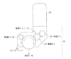
図2は、現像部20の一構成例を表すものである。なお、この図では、現像部20に加え、トナー収容部29をも描いている。現像部20は、感光ドラム21と、帯電ローラ22と、クリーニングブレード23と、現像ローラ24と、現像ブレード25と、供給ローラ26とを有している。   FIG. 2 illustrates a configuration example of the developing unit 20. In this figure, in addition to the developing unit 20, a toner storage unit 29 is also drawn. The developing unit 20 includes a photosensitive drum 21, a charging roller 22, a cleaning blade 23, a developing roller 24, a developing blade 25, and a supply roller 26.

感光ドラム21は、表面(表層部分)に静電潜像を担持する部材であり、感光体を用いて構成されるものである。感光ドラム21は、ドラムモータ20T(後述)から伝達された動力により、この例では右回りで回転する。感光ドラム21は、帯電ローラ22により帯電する。そして、現像部20Cの感光ドラム21は、露光ヘッド16Cにより露光され、現像部20Mの感光ドラム21は、露光ヘッド16Mにより露光され、現像部20Yの感光ドラム21は、露光ヘッド16Yにより露光され、現像部20Kの感光ドラム21は、露光ヘッド16Kにより露光される。このようにして、各感光ドラム21の表面には、静電潜像が形成されるようになっている。   The photosensitive drum 21 is a member that carries an electrostatic latent image on the surface (surface layer portion), and is configured using a photosensitive member. The photosensitive drum 21 rotates clockwise in this example by power transmitted from a drum motor 20T (described later). The photosensitive drum 21 is charged by the charging roller 22. The photosensitive drum 21 of the developing unit 20C is exposed by the exposure head 16C, the photosensitive drum 21 of the developing unit 20M is exposed by the exposure head 16M, and the photosensitive drum 21 of the developing unit 20Y is exposed by the exposure head 16Y. The photosensitive drum 21 of the developing unit 20K is exposed by the exposure head 16K. In this way, an electrostatic latent image is formed on the surface of each photosensitive drum 21.

帯電ローラ22は、感光ドラム21の表面(表層部分)を帯電させる部材である。帯電ローラ22は、感光ドラム21の表面(周面)に接するように配置されるとともに、所定の押し付け量で感光ドラム21に押し付けられように配置されている。帯電ローラ22は、感光ドラム21の回転に応じて、この例では左回りで回転する。帯電ローラ22には、高圧電源部55(後述)により帯電電圧が印加されるようになっている。   The charging roller 22 is a member that charges the surface (surface layer portion) of the photosensitive drum 21. The charging roller 22 is disposed so as to be in contact with the surface (circumferential surface) of the photosensitive drum 21 and is disposed so as to be pressed against the photosensitive drum 21 with a predetermined pressing amount. In this example, the charging roller 22 rotates counterclockwise according to the rotation of the photosensitive drum 21. A charging voltage is applied to the charging roller 22 by a high voltage power supply 55 (described later).

クリーニングブレード23は、感光ドラム21の表面(表層部分)に残留するトナーを掻き取ってクリーニングする部材である。このクリーニングブレード23は、感光ドラム21の表面に対してカウンタで(感光ドラム21の回転方向に対して逆向きで突出して)当接するように配置されるとともに、所定の押し付け量で感光ドラム21に押し付けられように配置されている。   The cleaning blade 23 is a member that scrapes off and removes toner remaining on the surface (surface layer portion) of the photosensitive drum 21. The cleaning blade 23 is disposed so as to come into contact with the surface of the photosensitive drum 21 with a counter (projecting in a direction opposite to the rotation direction of the photosensitive drum 21), and to the photosensitive drum 21 with a predetermined pressing amount. It is arranged to be pressed.

現像ローラ24は、トナーを表面に担持する部材である。この現像ローラ24は、感光ドラム21の表面(周面)に接するように配置されるとともに、所定の押し付け量で感光ドラム21に押し付けられように配置されている。現像ローラ24は、ドラムモータ20T(後述)から伝達された動力により、この例では左回りで回転する。各感光ドラム21では、現像ローラ24から供給されたトナーにより、静電潜像に応じたトナー像が形成(現像)される。現像ローラ24には、高圧電源部55(後述)により現像電圧が印加されるようになっている。   The developing roller 24 is a member that carries toner on the surface. The developing roller 24 is disposed so as to be in contact with the surface (circumferential surface) of the photosensitive drum 21 and is disposed so as to be pressed against the photosensitive drum 21 with a predetermined pressing amount. The developing roller 24 rotates counterclockwise in this example by power transmitted from a drum motor 20T (described later). In each photosensitive drum 21, a toner image corresponding to the electrostatic latent image is formed (developed) by the toner supplied from the developing roller 24. A developing voltage is applied to the developing roller 24 by a high voltage power supply 55 (described later).

現像ブレード25は、現像ローラ23の表面に当接することにより、この現像ローラ23の表面にトナーからなる層(トナー層)を形成させるとともに、そのトナー層の厚さを規制(制御,調整)する部材である。現像ブレード25は、例えば、ステンレス等からなる板状弾性部材をL字形状に折り曲げたものである。現像ブレード25は、その折れ曲がった部分が現像ローラ24の表面に当接するように配置されるとともに、所定の押し付け量で現像ローラ24に押し付けられように配置されている。現像ブレード25には、高圧電源部55(後述)により供給電圧が印加されるようになっている。   The developing blade 25 abuts on the surface of the developing roller 23 to form a toner layer (toner layer) on the surface of the developing roller 23 and regulate (control, adjust) the thickness of the toner layer. It is a member. The developing blade 25 is obtained by bending a plate-like elastic member made of, for example, stainless steel into an L shape. The developing blade 25 is disposed such that the bent portion is in contact with the surface of the developing roller 24 and is disposed so as to be pressed against the developing roller 24 with a predetermined pressing amount. A supply voltage is applied to the developing blade 25 by a high voltage power supply 55 (described later).

供給ローラ26は、トナー収容部29内に貯蔵されたトナーを、現像ローラ24に対して供給する部材である。この供給ローラ26は、現像ローラ24の表面(周面)に接するように配置されるとともに、所定の押し付け量で現像ローラ24に押し付けられように配置されている。供給ローラ26は、ドラムモータ20T(後述)から伝達された動力により、この例では左回りで回転する。これにより、各現像部20では、供給ローラ26の表面と現像ローラ24の表面との間には摩擦が生じる。その結果、各現像部20では、トナーが、いわゆる摩擦帯電により帯電するようになっている。供給ローラ26には、高圧電源部55(後述)により供給電圧が印加されるようになっている。   The supply roller 26 is a member that supplies the toner stored in the toner storage unit 29 to the developing roller 24. The supply roller 26 is disposed so as to be in contact with the surface (circumferential surface) of the developing roller 24 and is disposed so as to be pressed against the developing roller 24 with a predetermined pressing amount. The supply roller 26 rotates counterclockwise in this example by power transmitted from a drum motor 20T (described later). Thereby, in each developing unit 20, friction is generated between the surface of the supply roller 26 and the surface of the developing roller 24. As a result, in each developing unit 20, the toner is charged by so-called frictional charging. A supply voltage is applied to the supply roller 26 by a high-voltage power supply 55 (described later).

露光ヘッド16C(図1)は、現像部20Cの感光ドラム21(後述)に対して光を照射する部材であり、露光ヘッド16Mは、現像部20Mの感光ドラム21に対して光を照射する部材であり、露光ヘッド16Yは、現像部20Yの感光ドラム21に対して光を照射する部材であり、露光ヘッド16Kは、現像部20Kの感光ドラム21に対して光を照射する部材である。これにより、これらの感光ドラム21は、露光ヘッド16C,16M,16Y,16Kにより露光され、感光ドラム21の表面に、静電潜像が形成されるようになっている。   The exposure head 16C (FIG. 1) is a member that irradiates light to a photosensitive drum 21 (described later) of the developing unit 20C, and the exposure head 16M is a member that irradiates light to the photosensitive drum 21 of the developing unit 20M. The exposure head 16Y is a member that irradiates light to the photosensitive drum 21 of the developing unit 20Y, and the exposure head 16K is a member that irradiates light to the photosensitive drum 21 of the developing unit 20K. As a result, the photosensitive drums 21 are exposed by the exposure heads 16C, 16M, 16Y, and 16K, and an electrostatic latent image is formed on the surface of the photosensitive drum 21.

転写部30は、4つの現像部20C,20M,20Y,20Kにより形成されたトナー像を、記録媒体9の被転写面上に転写する部材である。転写部30は、転写ローラ31C,31M,31Y,31Kと、転写ベルト32と、駆動ローラ33と、従動ローラ34とを有している。   The transfer unit 30 is a member that transfers the toner image formed by the four developing units 20C, 20M, 20Y, and 20K onto the transfer surface of the recording medium 9. The transfer unit 30 includes transfer rollers 31 </ b> C, 31 </ b> M, 31 </ b> Y, and 31 </ b> K, a transfer belt 32, a drive roller 33, and a driven roller 34.

転写ローラ31Cは、搬送路10を介して現像部20Cの感光ドラム21に対向配置されており、転写ローラ31Mは、搬送路10を介して現像部20Mの感光ドラム21に対向配置されており、転写ローラ31Yは、搬送路10を介して現像部20Yの感光ドラム21に対向配置されており、転写ローラ31Kは、搬送路10を介して現像部20Kの感光ドラム21に対向配置されている。転写ローラ31C,31M,31Y,31Kのそれぞれには、高圧電源部55(後述)により転写電圧が印加されるようになっている。   The transfer roller 31C is disposed to face the photosensitive drum 21 of the developing unit 20C via the conveyance path 10, and the transfer roller 31M is disposed to face the photosensitive drum 21 of the developing unit 20M via the conveyance path 10. The transfer roller 31Y is disposed to face the photosensitive drum 21 of the developing unit 20Y through the transport path 10, and the transfer roller 31K is disposed to face the photosensitive drum 21 of the developing unit 20K through the transport path 10. A transfer voltage is applied to each of the transfer rollers 31C, 31M, 31Y, and 31K by a high-voltage power supply 55 (described later).

転写ベルト32は、搬送路10に沿って記録媒体9を搬送するものである。転写ベルト32は、駆動ローラ33および従動ローラ34によって張設(張架)されている。そして、転写ベルト32は、駆動ローラ33の回転に応じて、搬送方向Fの方向に循環回転するようになっている。その際、転写ベルト32は、現像部20Cと転写ローラ31Cとの間、現像部20Mと転写ローラ31Mとの間、現像部20Yと転写ローラ31Yとの間、および現像部20Kと転写ローラ31Kとの間を移動するようになっている。   The transfer belt 32 conveys the recording medium 9 along the conveyance path 10. The transfer belt 32 is stretched (strung) by a driving roller 33 and a driven roller 34. The transfer belt 32 circulates and rotates in the transport direction F according to the rotation of the drive roller 33. At that time, the transfer belt 32 is connected between the developing unit 20C and the transfer roller 31C, between the developing unit 20M and the transfer roller 31M, between the developing unit 20Y and the transfer roller 31Y, and between the developing unit 20K and the transfer roller 31K. To move between.

駆動ローラ33は、転写ベルト32を循環回転させるものである。この例では、駆動ローラ33は、搬送方向Fにおいて、4つの現像部20の下流側に配置され、ベルトモータ33T(後述)から伝達された動力により、この例では左回りで回転する。これにより、駆動ローラ33は、転写ベルト32を搬送方向Fの方向へ循環回転させるようになっている。   The drive roller 33 circulates and rotates the transfer belt 32. In this example, the drive roller 33 is disposed downstream of the four developing units 20 in the transport direction F, and rotates counterclockwise in this example by power transmitted from a belt motor 33T (described later). As a result, the drive roller 33 circulates and rotates the transfer belt 32 in the transport direction F.

従動ローラ34は、転写ベルト32の循環回転に応じて、この例では左回りで従動回転するものである。この例では、従動ローラ34は、搬送方向Fにおいて、4つの現像部20の上流側に配置されている。   The driven roller 34 is driven to rotate counterclockwise in this example in accordance with the circulating rotation of the transfer belt 32. In this example, the driven roller 34 is arranged on the upstream side of the four developing units 20 in the transport direction F.

クリーニングブレード14は、転写ベルト31の被転写面に残留するトナーを掻き取ってクリーニングする部材である。そして、掻き取られたトナーは、クリーナ容器15に収容されるようになっている。   The cleaning blade 14 is a member that scrapes off and removes toner remaining on the transfer surface of the transfer belt 31. Then, the scraped toner is accommodated in the cleaner container 15.

定着部40は、記録媒体9に対し熱および圧力を付与することにより、記録媒体9上に転写されたトナー像を記録媒体9に定着させる部材である。定着部40は、ヒートローラ41と、加圧ローラ43と、サーミスタ44とを有している。ヒートローラ41は、その内部にヒータ42を含んで構成されており、記録媒体9上のトナーに対して熱を付与する部材である。ヒータ42は、例えば、ハロゲンヒータを用いることができる。なお、これに限定されるものではなく、これに代えて、例えばセラミックヒータなどを用いてもよい。加圧ローラ43は、ヒートローラ41との間に圧接部が形成されるように配置されており、記録媒体9上のトナーに対して圧力を付与する部材である。ヒートローラ41および加圧ローラ43は、ヒータモータ40T(後述)から伝達された動力により回転するようになっている。サーミスタ44は、定着部40の温度を検出するものである。これにより、定着部40では、記録媒体9上のトナーが、加熱され、融解し、加圧される。その結果、トナー像が記録媒体9上に定着するようになっている。   The fixing unit 40 is a member that fixes the toner image transferred onto the recording medium 9 to the recording medium 9 by applying heat and pressure to the recording medium 9. The fixing unit 40 includes a heat roller 41, a pressure roller 43, and a thermistor 44. The heat roller 41 includes a heater 42 inside, and is a member that applies heat to the toner on the recording medium 9. As the heater 42, for example, a halogen heater can be used. In addition, it is not limited to this, It replaces with this and may use a ceramic heater etc., for example. The pressure roller 43 is disposed so that a pressure contact portion is formed between the pressure roller 43 and the heat roller 41, and is a member that applies pressure to the toner on the recording medium 9. The heat roller 41 and the pressure roller 43 are rotated by power transmitted from a heater motor 40T (described later). The thermistor 44 detects the temperature of the fixing unit 40. Thereby, in the fixing unit 40, the toner on the recording medium 9 is heated, melted, and pressurized. As a result, the toner image is fixed on the recording medium 9.

画像形成装置1では、このようにして、記録媒体9に対して印刷が行われる。そして、印刷された記録媒体9は、媒体ガイド17により、搬送路10に沿って搬送され、排紙トレイ18上に積載されるようになっている。   In the image forming apparatus 1, printing is performed on the recording medium 9 in this way. The printed recording medium 9 is transported along the transport path 10 by the medium guide 17 and stacked on the paper discharge tray 18.

(画像形成装置1の制御機構)
図3は、画像形成装置1における制御機構の一例を表すものである。画像形成装置1は、インタフェース部51と、画像処理部52と、露光制御部53と、表示部54と、高圧電源部55と、低圧電源部60と、プリンタエンジン制御部59とを有している。
(Control mechanism of image forming apparatus 1)
FIG. 3 illustrates an example of a control mechanism in the image forming apparatus 1. The image forming apparatus 1 includes an interface unit 51, an image processing unit 52, an exposure control unit 53, a display unit 54, a high voltage power supply unit 55, a low voltage power supply unit 60, and a printer engine control unit 59. Yes.

インタフェース部51は、例えば、図示しないホストコンピュータから、例えばPDL(Page Description Language)等により記述された印刷データを受け取るとともに、このホストコンピュータとの間で各種制御信号のやりとりを行うものである。   For example, the interface unit 51 receives print data described in, for example, PDL (Page Description Language) from a host computer (not shown), and exchanges various control signals with the host computer.

画像処理部52は、印刷データを受け取ったことをプリンタエンジン制御部59に通知するとともに、プリンタエンジン制御部59からの指示に基づいて、インタフェース部51から供給された印刷データに基づいて所定の処理を行うことによりビットマップデータを生成するものである。   The image processing unit 52 notifies the printer engine control unit 59 that the print data has been received, and performs predetermined processing based on the print data supplied from the interface unit 51 based on an instruction from the printer engine control unit 59. By doing this, bitmap data is generated.

露光制御部53は、プリンタエンジン制御部59からの指示、および画像処理部52から供給されたビットマップデータに基づいて、露光ヘッド16C,16M,16Y,16Kの動作を制御するものである。   The exposure control unit 53 controls the operation of the exposure heads 16C, 16M, 16Y, and 16K based on the instruction from the printer engine control unit 59 and the bitmap data supplied from the image processing unit 52.

表示部54は、画像形成装置1の動作状態などを表示するものであり、例えば、液晶ディスプレイを用いて構成されるものである。   The display unit 54 displays an operation state of the image forming apparatus 1 and is configured using, for example, a liquid crystal display.

高圧電源部55は、プリンタエンジン制御部59からの指示に基づいて、現像部20C,20M,20Y,20Kの帯電ローラ22に印加する帯電電圧をそれぞれ生成し、現像部20C,20M,20Y,20Kの現像ローラ24に印加する現像電圧をそれぞれ生成し、現像部20C,20M,20Y,20Kの供給ローラ26に印加する供給電圧をそれぞれ生成し、転写ローラ32C,32M,32Y,32Kに印加する転写電圧をそれぞれ生成するものである。   The high voltage power supply unit 55 generates charging voltages to be applied to the charging rollers 22 of the developing units 20C, 20M, 20Y, and 20K based on an instruction from the printer engine control unit 59, and develops the developing units 20C, 20M, 20Y, and 20K. A developing voltage to be applied to the developing roller 24 is generated, a supply voltage to be applied to the supply roller 26 of the developing units 20C, 20M, 20Y, and 20K is generated, and a transfer voltage is applied to the transfer rollers 32C, 32M, 32Y, and 32K. Each voltage is generated.

低圧電源部60は、プリンタエンジン制御部59からの指示に基づいて、定着部40のヒータ42に電力を供給するものである。低圧電源部60については、後ほど詳細に説明する。   The low voltage power supply unit 60 supplies power to the heater 42 of the fixing unit 40 based on an instruction from the printer engine control unit 59. The low voltage power supply unit 60 will be described in detail later.

プリンタエンジン制御部59は、画像形成装置1の各ブロックを制御するものである。具体的には、プリンタエンジン制御部59は、画像処理部52を制御することにより、印刷データに基づいてビットマップデータを生成させる。そして、プリンタエンジン制御部59は、低圧電源部60を制御することにより、定着部40のヒータ42に電力を供給させるとともに、サーミスタ44における検出結果に基づいてヒータ42に供給する電力を調節する。そして、プリンタエンジン制御部59は、ホッピングモータ11Tを制御することによりホッピングローラ11を回転させ、レジストモータ12Tを制御することによりレジストローラ12を回転させ、ドラムモータ20Tを制御することにより現像部20C,20M,20Y,20K内の感光ドラム21、現像ローラ24、および供給ローラ26をそれぞれ回転させ、ベルトモータ33Tを制御することにより駆動ローラ106を回転させ、ヒータモータ40Tを制御することによりヒートローラ41および加圧ローラ43を回転させる。また、プリンタエンジン制御部59は、媒体センサ13における検出結果に基づいて、高圧電源部55を制御することにより各種電圧を生成させる。そして、プリンタエンジン制御部59は、露光制御部53の動作を制御することにより露光ヘッド16C,16M,16Y,16Kを動作させる。また、プリンタエンジン制御部59は、表示部54を制御することにより、画像形成装置1の動作状態などを表示させるようになっている。   The printer engine control unit 59 controls each block of the image forming apparatus 1. Specifically, the printer engine control unit 59 controls the image processing unit 52 to generate bitmap data based on the print data. The printer engine control unit 59 controls the low-voltage power supply unit 60 to supply power to the heater 42 of the fixing unit 40 and adjust the power supplied to the heater 42 based on the detection result in the thermistor 44. Then, the printer engine control unit 59 rotates the hopping roller 11 by controlling the hopping motor 11T, rotates the registration roller 12 by controlling the registration motor 12T, and controls the drum motor 20T to develop the developing unit 20C. , 20M, 20Y, and 20K, the photosensitive drum 21, the developing roller 24, and the supply roller 26 are respectively rotated, the driving roller 106 is rotated by controlling the belt motor 33T, and the heat roller is controlled by controlling the heater motor 40T. 41 and the pressure roller 43 are rotated. Further, the printer engine control unit 59 generates various voltages by controlling the high-voltage power supply unit 55 based on the detection result of the medium sensor 13. Then, the printer engine control unit 59 controls the operation of the exposure control unit 53 to operate the exposure heads 16C, 16M, 16Y, and 16K. Further, the printer engine control unit 59 displays the operation state of the image forming apparatus 1 by controlling the display unit 54.

プリンタエンジン制御部59は、低圧電源部60を制御する際、電力指示信号CTLおよび出力イネーブル信号ENBを低圧電源部60に供給する。電力指示信号CTLは、ヒータ42への電力供給量を指示するものである。出力イネーブル信号ENBは、ヒータ42への電力供給を行うか否かを指示するものである。具体的には、例えば、プリンタエンジン制御部59は、サーミスタ44における検出結果に基づいて、ヒータ42の温度が一定になるように、電力指示信号CTLおよび出力イネーブル信号ENBを用いて指示する。また、プリンタエンジン制御部59は、例えば、ヒータ42に電力を供給し始める場合には、電力供給量を徐々に増やすように、電力指示信号CTLを用いて指示する。すなわち、ヒータ42に対して冷えた状態で通電を開始すると、ヒータ42の抵抗値が低いため、突入電流が大きくなってしまう。そこで、プリンタエンジン制御部59は、まず最初は、電力供給量を低く設定し、ヒータ42が温まり電流が下がってきたら、電力供給量を増やす。このようにして、プリンタエンジン制御部59は、ヒータ42に電力を供給し始める際は、電力供給量を徐々に高くするようになっている。   When controlling the low-voltage power supply unit 60, the printer engine control unit 59 supplies the power instruction signal CTL and the output enable signal ENB to the low-voltage power supply unit 60. The power instruction signal CTL instructs the power supply amount to the heater 42. The output enable signal ENB instructs whether or not to supply power to the heater 42. Specifically, for example, the printer engine control unit 59 instructs using the power instruction signal CTL and the output enable signal ENB so that the temperature of the heater 42 becomes constant based on the detection result in the thermistor 44. Further, for example, when the printer engine control unit 59 starts to supply power to the heater 42, the printer engine control unit 59 uses the power instruction signal CTL to instruct to gradually increase the power supply amount. That is, when energization is started with the heater 42 being cooled, the resistance value of the heater 42 is low, and the inrush current increases. Therefore, the printer engine control unit 59 first sets the power supply amount to be low, and increases the power supply amount when the heater 42 is warmed and the current decreases. In this way, the printer engine control unit 59 gradually increases the power supply amount when starting to supply power to the heater 42.

(低圧電源部60)
図4は、低圧電源部60の一構成例を表すものである。この図では、低圧電源部60に加え、商用電源99、ヒータ42、およびプリンタエンジン制御部59をも描いている。低圧電源部60は、商用電源99から供給される交流信号Sac1に基づいて、交流信号Sac2を生成し、その交流信号Sac2をヒータ42に供給するものである。この例では、商用電源99から供給される交流信号Sac1の周波数は50Hzであり、実効値は100Vrmsである。なお、これに限定されるものではなく、周波数は、例えば60Hzであってもよいし、実効値は、例えば200Vrmsであってもよい。低圧電源部60は、力率改善回路(Power Factor Correction回路)100と、ゼロクロス検出回路200と、DC−DCコンバータ61と、DC−ACインバータ62とを有している。
(Low voltage power supply 60)
FIG. 4 illustrates a configuration example of the low-voltage power supply unit 60. In this figure, in addition to the low-voltage power supply unit 60, the commercial power supply 99, the heater 42, and the printer engine control unit 59 are also drawn. The low-voltage power supply unit 60 generates an AC signal Sac2 based on the AC signal Sac1 supplied from the commercial power supply 99, and supplies the AC signal Sac2 to the heater 42. In this example, the frequency of the AC signal Sac1 supplied from the commercial power supply 99 is 50 Hz, and the effective value is 100 Vrms. Note that the frequency is not limited to this, and the frequency may be, for example, 60 Hz, and the effective value may be, for example, 200 Vrms. The low-voltage power supply unit 60 includes a power factor correction circuit 100, a zero-cross detection circuit 200, a DC-DC converter 61, and a DC-AC inverter 62.

(力率改善回路100)
力率改善回路100は、交流信号Sac1に基づいて信号Sdc390を生成するものである。信号Sdc390の電圧は、この例では390Vである。なお、この電圧に限定されるものではなく、390V以外の電圧であってもよい。以下に、力率改善回路100について詳細に説明する。
(Power factor correction circuit 100)
The power factor correction circuit 100 generates a signal Sdc390 based on the AC signal Sac1. The voltage of the signal Sdc390 is 390V in this example. In addition, it is not limited to this voltage, A voltage other than 390V may be sufficient. Hereinafter, the power factor correction circuit 100 will be described in detail.

図5は、力率改善回路100の一構成例を表すものである。力率改善回路100は、ヒューズ91およびコモンモードチョークコイル92を介して商用電源99と接続されている。具体的には、商用電源99の一端はコモンモードチョークコイル92の第1の巻線の一端に接続され、他端はヒューズ91の一端に接続されている。ヒューズ91の一端は商用電源99の他端に接続され、他端はコモンモードチョークコイル92の第2の巻線の一端に接続されている。コモンモードチョークコイル92の第1の巻線の一端は商用電源99の一端に接続され、他端は力率改善回路100およびゼロクロス検出回路200に接続されている。コモンモードチョークコイル92の第2の巻線の一端はヒューズ91の他端に接続され、他端は力率改善回路100およびゼロクロス検出回路200に接続されている。   FIG. 5 illustrates a configuration example of the power factor correction circuit 100. The power factor correction circuit 100 is connected to a commercial power source 99 via a fuse 91 and a common mode choke coil 92. Specifically, one end of the commercial power source 99 is connected to one end of the first winding of the common mode choke coil 92, and the other end is connected to one end of the fuse 91. One end of the fuse 91 is connected to the other end of the commercial power source 99, and the other end is connected to one end of the second winding of the common mode choke coil 92. One end of the first winding of the common mode choke coil 92 is connected to one end of the commercial power source 99, and the other end is connected to the power factor correction circuit 100 and the zero cross detection circuit 200. One end of the second winding of the common mode choke coil 92 is connected to the other end of the fuse 91, and the other end is connected to the power factor correction circuit 100 and the zero cross detection circuit 200.

力率改善回路100は、ブリッジダイオード101と、スイッチング回路110,120と、ダイオード102,103と、電解コンデンサ104と、抵抗素子105〜108と、ダイオード131,132と、抵抗素子133,134と、コンデンサ135と、抵抗素子136,137と、制御回路140とを有している。力率改善回路100には、DC−DCコンバータ400B(後述)から、端子T191を介して、信号Sdc15B,Sdc0Bが供給される。この信号Sdc15Bの電圧は、信号Sdc0Bの電圧よりも15V高いものである。また、力率改善回路100は、端子T192を介して、信号Sdc390,Sdc0Bを出力するようになっている。   The power factor correction circuit 100 includes a bridge diode 101, switching circuits 110 and 120, diodes 102 and 103, an electrolytic capacitor 104, resistance elements 105 to 108, diodes 131 and 132, resistance elements 133 and 134, A capacitor 135, resistance elements 136 and 137, and a control circuit 140 are included. Signals Sdc15B and Sdc0B are supplied to the power factor correction circuit 100 from a DC-DC converter 400B (described later) via a terminal T191. The voltage of the signal Sdc15B is 15V higher than the voltage of the signal Sdc0B. The power factor correction circuit 100 outputs signals Sdc390 and Sdc0B via a terminal T192.

ブリッジダイオード101は、コモンモードチョークコイル92から出力される交流信号に対して全波整流を行うものである。ブリッジダイオード101の第1のダイオードのカソードおよび第2のダイオードのアノードは、コモンモードチョークコイル92の第1の巻線の他端に接続され、ブリッジダイオード101の第3のダイオードのカソードおよび第4のダイオードのアノードは、コモンモードチョークコイル92の第2の巻線の他端に接続されている。ブリッジダイオード101の第1のダイオードのアノードおよび第3のダイオードのアノードには信号Sdc0Bが供給されている。ブリッジダイオード101の第2のダイオードのカソードおよび第4のダイオードのカソードには、スイッチング回路110,120が接続されている。   The bridge diode 101 performs full-wave rectification on the AC signal output from the common mode choke coil 92. The cathode of the first diode of the bridge diode 101 and the anode of the second diode are connected to the other end of the first winding of the common mode choke coil 92, and the cathode and the fourth diode of the third diode of the bridge diode 101. The anode of this diode is connected to the other end of the second winding of the common mode choke coil 92. The signal Sdc0B is supplied to the anode of the first diode and the anode of the third diode of the bridge diode 101. Switching circuits 110 and 120 are connected to the cathode of the second diode and the cathode of the fourth diode of the bridge diode 101.

スイッチング回路110は、ゲートドライブ信号GD1に基づいてスイッチング動作を行うものである。   The switching circuit 110 performs a switching operation based on the gate drive signal GD1.

図6は、スイッチング回路110の一構成例を表すものである。スイッチング回路110は、抵抗素子114,115と、NPNトランジスタ116と、PNPトランジスタ117と、抵抗素子118,119と、インダクタ111と、絶縁ゲートバイポーラトランジスタ(IGBT)112と、ダイオード112Dと、抵抗素子113とを有している。なお、図5では、これらの素子のうち、インダクタ111、IGBT112、抵抗素子113を描いている。   FIG. 6 illustrates a configuration example of the switching circuit 110. The switching circuit 110 includes resistance elements 114 and 115, an NPN transistor 116, a PNP transistor 117, resistance elements 118 and 119, an inductor 111, an insulated gate bipolar transistor (IGBT) 112, a diode 112D, and a resistance element 113. And have. In FIG. 5, among these elements, the inductor 111, the IGBT 112, and the resistance element 113 are drawn.

抵抗素子114の一端にはゲートドライブ信号GD1が供給され、他端はNPNトランジスタ116のベースおよびPNPトランジスタ117のベースに接続されている。抵抗素子115の一端には信号Sdc15Bが供給され、他端はNPNトランジスタ116のコレクタに接続されている。NPNトランジスタ116のコレクタは抵抗素子115の他端に接続され、ベースは抵抗素子114の他端およびPNPトランジスタ117のベースに接続され、エミッタはPNPトランジスタ117のエミッタおよび抵抗素子118の一端に接続されている。PNPトランジスタ117のエミッタはNPNトランジスタ116のエミッタおよび抵抗素子118の一端に接続され、ベースは抵抗素子114の他端およびNPNトランジスタ116のベースに接続され、コレクタは抵抗素子119の他端、IGBT112のエミッタ、ダイオード112Dのアノード、および抵抗素子113の一端に接続されている。抵抗素子118の一端はNPNトランジスタ116のエミッタおよびPNPトランジスタ117のエミッタに接続され、他端は抵抗素子119の一端およびIGBT112のベースに接続されている。抵抗素子119の一端は抵抗素子118の他端およびIGBT112のベースに接続され、他端はPNPトランジスタ117のコレクタ、IGBT112のエミッタ、ダイオード112Dのアノード、および抵抗素子113の一端に接続されている。インダクタ111の一端は、図5に示したようにブリッジダイオード101の第2のダイオードのカソードおよび第4のダイオードのカソードに接続され、他端はIGBT112のコレクタおよびダイオード112Dのカソードに接続されている。IGBT112のコレクタはインダクタ111の他端およびダイオード112Dのカソードに接続され、ベースは抵抗素子118の他端および抵抗素子119の一端に接続され、エミッタはPNPトランジスタ117のコレクタ、抵抗素子119の他端、ダイオード112Dのアノード、および抵抗素子113の一端に接続されている。ダイオード112DのアノードはIGBT112のエミッタ、PNPトランジスタ117のコレクタ、抵抗素子119の他端、および抵抗素子113の一端に接続され、カソードはインダクタ111の他端およびIGBT112のコレクタに接続されている。抵抗素子113の一端はPNPトランジスタ117のコレクタ、抵抗素子119の他端、IGBT112のエミッタ、およびダイオード112Dのアノードに接続され、他端には信号Sdc0Bが供給されている。抵抗素子113の一端における電圧は、信号DET1として制御回路140に供給されるようになっている。   One end of the resistance element 114 is supplied with the gate drive signal GD 1, and the other end is connected to the base of the NPN transistor 116 and the base of the PNP transistor 117. One end of the resistance element 115 is supplied with the signal Sdc15B, and the other end is connected to the collector of the NPN transistor 116. The collector of NPN transistor 116 is connected to the other end of resistance element 115, the base is connected to the other end of resistance element 114 and the base of PNP transistor 117, and the emitter is connected to the emitter of PNP transistor 117 and one end of resistance element 118. ing. The emitter of the PNP transistor 117 is connected to the emitter of the NPN transistor 116 and one end of the resistor element 118, the base is connected to the other end of the resistor element 114 and the base of the NPN transistor 116, the collector is the other end of the resistor element 119, and the IGBT 112 The emitter, the anode of the diode 112D, and one end of the resistance element 113 are connected. One end of the resistance element 118 is connected to the emitter of the NPN transistor 116 and the emitter of the PNP transistor 117, and the other end is connected to one end of the resistance element 119 and the base of the IGBT 112. One end of the resistance element 119 is connected to the other end of the resistance element 118 and the base of the IGBT 112, and the other end is connected to the collector of the PNP transistor 117, the emitter of the IGBT 112, the anode of the diode 112 </ b> D, and one end of the resistance element 113. As shown in FIG. 5, one end of the inductor 111 is connected to the cathode of the second diode and the cathode of the fourth diode of the bridge diode 101, and the other end is connected to the collector of the IGBT 112 and the cathode of the diode 112D. . The collector of IGBT 112 is connected to the other end of inductor 111 and the cathode of diode 112D, the base is connected to the other end of resistance element 118 and one end of resistance element 119, and the emitter is the collector of PNP transistor 117 and the other end of resistance element 119. , The anode of the diode 112D, and one end of the resistance element 113. The anode of the diode 112D is connected to the emitter of the IGBT 112, the collector of the PNP transistor 117, the other end of the resistance element 119, and one end of the resistance element 113, and the cathode is connected to the other end of the inductor 111 and the collector of the IGBT 112. One end of the resistance element 113 is connected to the collector of the PNP transistor 117, the other end of the resistance element 119, the emitter of the IGBT 112, and the anode of the diode 112D, and the signal Sdc0B is supplied to the other end. The voltage at one end of the resistance element 113 is supplied to the control circuit 140 as the signal DET1.

スイッチング回路120(図5)は、ゲートドライブ信号GD2に基づいてスイッチング動作を行うものである。スイッチング回路120は、スイッチング回路110(図6)と同様の構成を有するものである。スイッチング回路120は、インダクタ121と、IGBT122と、抵抗素子123とを有している。インダクタ121、IGBT122、および抵抗素子123は、スイッチング回路110におけるインダクタ111、IGBT112、および抵抗素子113に対応するものである。抵抗素子123の一端における電圧は、信号DET2として制御回路140に供給されるようになっている。   The switching circuit 120 (FIG. 5) performs a switching operation based on the gate drive signal GD2. The switching circuit 120 has the same configuration as the switching circuit 110 (FIG. 6). The switching circuit 120 includes an inductor 121, an IGBT 122, and a resistance element 123. Inductor 121, IGBT 122, and resistance element 123 correspond to inductor 111, IGBT 112, and resistance element 113 in switching circuit 110. The voltage at one end of the resistance element 123 is supplied to the control circuit 140 as the signal DET2.

ダイオード102のアノードはインダクタ111の他端等に接続され、カソードはダイオード103のカソード、電解コンデンサ104の正極端子、抵抗素子105の一端、および抵抗素子107の一端に接続されている。ダイオード103のアノードはインダクタ121の他端等に接続され、カソードはダイオード102のカソード、電解コンデンサ104の正極端子、抵抗素子105の一端、および抵抗素子107の一端に接続されている。電解コンデンサ104の正極端子は、ダイオード102のカソード、ダイオード103のカソード、抵抗素子105の一端、および抵抗素子107の一端に接続され、負極端子には信号Sdc0Bが供給されている。電解コンデンサ104の正極端子における電圧は、信号Sdc390として、端子T192を介して出力されるようになっている。   The anode of the diode 102 is connected to the other end of the inductor 111, and the cathode is connected to the cathode of the diode 103, the positive terminal of the electrolytic capacitor 104, one end of the resistance element 105, and one end of the resistance element 107. The anode of the diode 103 is connected to the other end of the inductor 121 and the cathode is connected to the cathode of the diode 102, the positive terminal of the electrolytic capacitor 104, one end of the resistance element 105, and one end of the resistance element 107. The positive terminal of the electrolytic capacitor 104 is connected to the cathode of the diode 102, the cathode of the diode 103, one end of the resistance element 105, and one end of the resistance element 107, and a signal Sdc0B is supplied to the negative terminal. The voltage at the positive terminal of the electrolytic capacitor 104 is output as a signal Sdc390 via a terminal T192.

抵抗素子105の一端は、ダイオード102のカソード、ダイオード103のカソード、電解コンデンサ104の正極端子、および抵抗素子107の一端に接続され、他端は抵抗素子106の一端に接続されている。抵抗素子106の一端は抵抗素子105の他端に接続され、他端には信号Sdc0Bが供給されている。抵抗素子105の他端および抵抗素子106の一端における電圧は、信号OVPとして制御回路140に供給されるようになっている。   One end of the resistance element 105 is connected to the cathode of the diode 102, the cathode of the diode 103, the positive terminal of the electrolytic capacitor 104, and one end of the resistance element 107, and the other end is connected to one end of the resistance element 106. One end of the resistance element 106 is connected to the other end of the resistance element 105, and a signal Sdc0B is supplied to the other end. The voltage at the other end of the resistance element 105 and one end of the resistance element 106 is supplied to the control circuit 140 as a signal OVP.

抵抗素子107の一端は、ダイオード102のカソード、ダイオード103のカソード、電解コンデンサ104の正極端子、および抵抗素子105の一端に接続され、他端は抵抗素子108の一端に接続されている。抵抗素子108の一端は抵抗素子107の他端に接続され、他端には信号Sdc0Bが供給されている。抵抗素子107の他端および抵抗素子108の一端における電圧は、信号FBとして制御回路140に供給されるようになっている。   One end of the resistance element 107 is connected to the cathode of the diode 102, the cathode of the diode 103, the positive terminal of the electrolytic capacitor 104, and one end of the resistance element 105, and the other end is connected to one end of the resistance element 108. One end of the resistance element 108 is connected to the other end of the resistance element 107, and a signal Sdc0B is supplied to the other end. The voltage at the other end of the resistance element 107 and one end of the resistance element 108 is supplied to the control circuit 140 as a signal FB.

ダイオード131,132からなる回路は、コモンモードチョークコイル92から出力される交流信号に対して全波整流を行うものである。ダイオード131のアノードはコモンモードチョークコイル92の第1の巻線の他端に接続され、カソードはダイオード132のカソード、抵抗素子133の一端、および抵抗素子136の一端に接続されている。ダイオード132のアノードはコモンモードチョークコイル92の第2の巻線の他端に接続され、カソードはダイオード131のカソード、抵抗素子133の一端、および抵抗素子136の一端に接続されている。   The circuit composed of the diodes 131 and 132 performs full-wave rectification on the AC signal output from the common mode choke coil 92. The anode of the diode 131 is connected to the other end of the first winding of the common mode choke coil 92, and the cathode is connected to the cathode of the diode 132, one end of the resistance element 133, and one end of the resistance element 136. The anode of the diode 132 is connected to the other end of the second winding of the common mode choke coil 92, and the cathode is connected to the cathode of the diode 131, one end of the resistance element 133, and one end of the resistance element 136.

抵抗素子133の一端はダイオード131のカソード、ダイオード132のカソード、および抵抗素子136の一端に接続され、他端は抵抗素子134の一端およびコンデンサ135の一端に接続されている。抵抗素子134の一端は抵抗素子133の他端およびコンデンサ135の一端に接続され、他端には信号Sdc0Bが供給されている。コンデンサ135の一端は抵抗素子133の他端および抵抗素子134の一端に接続され、他端には信号Sdc0Bが供給されている。抵抗素子133の他端、抵抗素子134の一端、およびコンデンサ135の一端における電圧は、信号STとして制御回路140に供給されるようになっている。   One end of the resistor element 133 is connected to the cathode of the diode 131, the cathode of the diode 132, and one end of the resistor element 136, and the other end is connected to one end of the resistor element 134 and one end of the capacitor 135. One end of the resistance element 134 is connected to the other end of the resistance element 133 and one end of the capacitor 135, and a signal Sdc0B is supplied to the other end. One end of the capacitor 135 is connected to the other end of the resistance element 133 and one end of the resistance element 134, and a signal Sdc0B is supplied to the other end. The voltage at the other end of the resistance element 133, one end of the resistance element 134, and one end of the capacitor 135 is supplied to the control circuit 140 as a signal ST.

抵抗素子136の一端はダイオード131のカソード、ダイオード132のカソード、および抵抗素子133の一端に接続され、他端は抵抗素子137の一端に接続されている。抵抗素子137の一端は抵抗素子136の他端に接続され、他端には信号Sdc0Bが供給されている。抵抗素子136の他端および抵抗素子137の一端における電圧は、信号ACINとして制御回路140に供給されるようになっている。   One end of the resistance element 136 is connected to the cathode of the diode 131, the cathode of the diode 132, and one end of the resistance element 133, and the other end is connected to one end of the resistance element 137. One end of the resistance element 137 is connected to the other end of the resistance element 136, and a signal Sdc0B is supplied to the other end. The voltage at the other end of the resistance element 136 and one end of the resistance element 137 is supplied to the control circuit 140 as a signal ACIN.

制御回路140は、スイッチング回路110に対してゲートドライブ信号GD1を供給するとともに、スイッチング回路120に対してゲートドライブ信号GD2を供給することにより、力率改善回路100が信号Sdc390を生成するように制御するものである。具体的には、制御回路140は、信号FBに基づいて、ゲートドライブ信号GD1,GD2のスイッチングデューティ比を変化させ、信号Sdc390の電圧が所望の電圧(この例では390V)になるように制御するとともに、信号OVPに基づいて、信号Sdc390の電圧が過大にならないように制御する。その際、制御回路140は、信号ACINに基づいて、力率が1付近(例えば0.9以上)になるように、スイッチング回路110,120におけるスイッチング動作を制御するようになっている。   The control circuit 140 supplies the gate drive signal GD1 to the switching circuit 110 and supplies the gate drive signal GD2 to the switching circuit 120, thereby controlling the power factor correction circuit 100 to generate the signal Sdc390. To do. Specifically, the control circuit 140 changes the switching duty ratio of the gate drive signals GD1 and GD2 based on the signal FB so as to control the voltage of the signal Sdc390 to be a desired voltage (390 V in this example). At the same time, based on the signal OVP, control is performed so that the voltage of the signal Sdc390 does not become excessive. At that time, the control circuit 140 controls the switching operation in the switching circuits 110 and 120 based on the signal ACIN so that the power factor is around 1 (for example, 0.9 or more).

また、制御回路140は、信号DET1に基づいてIGBT112に過大な電流が流れていないか否かを監視するとともに、信号DET2に基づいてIGBT122に過大な電流が流れていないか否かを監視する機能をも有している。そして、制御回路140は、過大な電流が流れている場合には、スイッチング回路110,120におけるスイッチング動作を停止するようになっている。また、制御回路140は、信号STに基づいて、交流信号Sac1の振幅が所定の振幅以上である場合において、スイッチング回路110,120に対してスイッチング動作を行わせるようになっている。   Further, the control circuit 140 monitors whether or not an excessive current flows through the IGBT 112 based on the signal DET1, and monitors whether or not an excessive current flows through the IGBT 122 based on the signal DET2. It also has. The control circuit 140 stops the switching operation in the switching circuits 110 and 120 when an excessive current flows. Further, the control circuit 140 causes the switching circuits 110 and 120 to perform a switching operation based on the signal ST when the amplitude of the AC signal Sac1 is greater than or equal to a predetermined amplitude.

(ゼロクロス検出回路200)
ゼロクロス検出回路200(図4)は、交流信号Sac1に基づいてゼロクロス信号SZを生成するものである。以下に、ゼロクロス検出回路200について詳細に説明する。
(Zero cross detection circuit 200)
The zero cross detection circuit 200 (FIG. 4) generates the zero cross signal SZ based on the AC signal Sac1. Hereinafter, the zero cross detection circuit 200 will be described in detail.

図7は、ゼロクロス検出回路200の一構成例を表すものである。ゼロクロス検出回路200は、力率改善回路100と同様に、ヒューズ91およびコモンモードチョークコイル92を介して商用電源99と接続されている。   FIG. 7 illustrates a configuration example of the zero cross detection circuit 200. The zero-cross detection circuit 200 is connected to the commercial power supply 99 via the fuse 91 and the common mode choke coil 92, similarly to the power factor correction circuit 100.

ゼロクロス検出回路200は、抵抗素子201,202と、コンデンサ203と、ブリッジダイオード204と、フォトカプラ205と、抵抗素子206と、Nチャネル電界効果トランジスタ(FET)207と、抵抗素子208〜210と、NPNトランジスタ211と、抵抗素子212と、D型フリップフロップ213とを有している。ゼロクロス検出回路20には、DC−DCコンバータ61から信号Sdc5が供給される。この信号Sdc5の電圧は、この例では5Vである。   The zero-cross detection circuit 200 includes resistance elements 201 and 202, a capacitor 203, a bridge diode 204, a photocoupler 205, a resistance element 206, an N-channel field effect transistor (FET) 207, resistance elements 208 to 210, It has an NPN transistor 211, a resistance element 212, and a D-type flip-flop 213. The zero cross detection circuit 20 is supplied with a signal Sdc5 from the DC-DC converter 61. The voltage of this signal Sdc5 is 5V in this example.

抵抗素子201の一端はコモンモードチョークコイル92の第1の巻線の他端に接続され、他端は抵抗素子202の一端およびコンデンサ203の一端に接続されている。抵抗素子202の一端は抵抗素子201の他端およびコンデンサ203の一端に接続され、他端はブリッジダイオード204の第1のダイオードのカソードおよび第2のダイオードのアノードに接続されている。コンデンサ203の一端は抵抗素子201の他端および抵抗素子202の一端に接続され、他端はコモンモードチョークコイル92の第2の巻線の他端、ブリッジダイオード204の第3のダイオードのカソードおよび第4のダイオードのアノードに接続されている。   One end of the resistance element 201 is connected to the other end of the first winding of the common mode choke coil 92, and the other end is connected to one end of the resistance element 202 and one end of the capacitor 203. One end of the resistance element 202 is connected to the other end of the resistance element 201 and one end of the capacitor 203, and the other end is connected to the cathode of the first diode and the anode of the second diode of the bridge diode 204. One end of the capacitor 203 is connected to the other end of the resistance element 201 and one end of the resistance element 202, and the other end is the other end of the second winding of the common mode choke coil 92, the cathode of the third diode of the bridge diode 204, and Connected to the anode of the fourth diode.

ブリッジダイオード204は、抵抗素子202の他端とコンデンサ203の他端との間の信号に対して全波整流を行うものである。ブリッジダイオード204の第1のダイオードのカソードおよび第2のダイオードのアノードは、抵抗素子202の他端に接続され、ブリッジダイオード204の第3のダイオードのカソードおよび第4のダイオードのアノードは、コンデンサ203の他端に接続されている。ブリッジダイオード204の第1のダイオードのアノードおよび第3のダイオードのアノードは、フォトカプラ205の発光ダイオードのカソードに接続されている。ブリッジダイオード204の第2のダイオードのカソードおよび第4のダイオードのカソードは、フォトカプラ205の発光ダイオードのアノードに接続されている。   The bridge diode 204 performs full-wave rectification on a signal between the other end of the resistance element 202 and the other end of the capacitor 203. The cathode of the first diode and the anode of the second diode of the bridge diode 204 are connected to the other end of the resistance element 202, and the cathode of the third diode and the anode of the fourth diode of the bridge diode 204 are connected to the capacitor 203. Is connected to the other end. The anode of the first diode and the anode of the third diode of the bridge diode 204 are connected to the cathode of the light emitting diode of the photocoupler 205. The cathode of the second diode and the cathode of the fourth diode of the bridge diode 204 are connected to the anode of the light emitting diode of the photocoupler 205.

フォトカプラ205の発光ダイオードのアノードはブリッジダイオード204の第2のダイオードのカソードおよび第4のダイオードのカソードに接続され、発光ダイオードのカソードはブリッジダイオード204の第1のダイオードのアノードおよび第3のダイオードのアノードに接続されている。フォトカプラ205のフォトダイオードのエミッタは接地され、コレクタは抵抗素子206の他端およびNチャネルFET207のゲートに接続されている。   The anode of the light emitting diode of the photocoupler 205 is connected to the cathode of the second diode and the cathode of the fourth diode of the bridge diode 204, and the cathode of the light emitting diode is the anode of the first diode and the third diode of the bridge diode 204. Connected to the anode. The photodiode emitter of the photocoupler 205 is grounded, and the collector is connected to the other end of the resistance element 206 and the gate of the N-channel FET 207.

抵抗素子206の一端には信号Sdc5が供給され、他端はフォトカプラ205のフォトダイオードのコレクタおよびNチャネルFET207のゲートに接続されている。NチャネルFET207のドレインは抵抗素子208の他端および抵抗素子209の一端に接続され、ゲートはフォトカプラ205のフォトダイオードのコレクタおよび抵抗素子206の他端に接続され、ソースは接地されている。抵抗素子208の一端には信号Sdc5が供給され、他端はNチャネルFETのドレインおよび抵抗素子209の一端に接続されている。抵抗素子209の一端はNチャネルFET207のドレインおよび抵抗素子208の他端に接続され、他端はNPNトランジスタ211のベースおよび抵抗素子210の一端に接続されている。抵抗素子210の一端は抵抗素子209の他端およびNPNトランジスタ211のベースに接続され、他端は接地されている。NPNトランジスタ211のコレクタは抵抗素子212の他端およびD型フリップフロップ213のクロック入力端子に接続され、ベースは抵抗素子209の他端および抵抗素子210の一端に接続され、エミッタは接地されている。抵抗素子212の一端には信号Sdc5が供給され、他端はNPNトランジスタ211のコレクタおよびD型フリップフロップ213のクロック入力端子に接続されている。   A signal Sdc5 is supplied to one end of the resistance element 206, and the other end is connected to the collector of the photodiode of the photocoupler 205 and the gate of the N-channel FET 207. The drain of the N-channel FET 207 is connected to the other end of the resistance element 208 and one end of the resistance element 209, the gate is connected to the collector of the photodiode of the photocoupler 205 and the other end of the resistance element 206, and the source is grounded. A signal Sdc5 is supplied to one end of the resistance element 208, and the other end is connected to the drain of the N-channel FET and one end of the resistance element 209. One end of the resistance element 209 is connected to the drain of the N-channel FET 207 and the other end of the resistance element 208, and the other end is connected to the base of the NPN transistor 211 and one end of the resistance element 210. One end of the resistance element 210 is connected to the other end of the resistance element 209 and the base of the NPN transistor 211, and the other end is grounded. The collector of the NPN transistor 211 is connected to the other end of the resistor element 212 and the clock input terminal of the D-type flip-flop 213, the base is connected to the other end of the resistor element 209 and one end of the resistor element 210, and the emitter is grounded. . A signal Sdc5 is supplied to one end of the resistance element 212, and the other end is connected to the collector of the NPN transistor 211 and the clock input terminal of the D-type flip-flop 213.

D型フリップフロップ213のクロック入力端子は抵抗素子212の他端およびNPNトランジスタ211のコレクタに接続され、データ入力端子は、反転データ出力端子に接続されている。そして、D型フリップフロップ213は、データ出力端子からゼロクロス信号SZを出力するようになっている。   The clock input terminal of the D-type flip-flop 213 is connected to the other end of the resistance element 212 and the collector of the NPN transistor 211, and the data input terminal is connected to the inverted data output terminal. The D-type flip-flop 213 outputs a zero cross signal SZ from the data output terminal.

この構成により、ゼロクロス検出回路200は、交流信号Sac1のゼロクロスタイミングごとに反転するゼロクロス信号SZを生成するようになっている。   With this configuration, the zero cross detection circuit 200 generates a zero cross signal SZ that is inverted at each zero cross timing of the AC signal Sac1.

(DC−DCコンバータ61)
DC−DCコンバータ61(図4)は、信号Sdc390に基づいて、信号Sdc24,Sdc5を生成するものである。信号Sdc24の電圧は、この例では24Vである。信号Sdc24,Sdc5は、画像形成装置1内の様々なブロックで用いられるものである。DC−DCコンバータ61は、公知の技術を用いて構成されるものである。
(DC-DC converter 61)
The DC-DC converter 61 (FIG. 4) generates signals Sdc24 and Sdc5 based on the signal Sdc390. The voltage of the signal Sdc24 is 24V in this example. The signals Sdc24 and Sdc5 are used in various blocks in the image forming apparatus 1. The DC-DC converter 61 is configured using a known technique.

(DC−ACインバータ62)
DC−ACインバータ62は、信号Sdc390、ゼロクロス信号SZ、およびプリンタエンジン制御部59からの指示に基づいて、交流信号Sac2を生成するものである。具体的には、後述するように、DC−ACインバータ62は、信号Sdc390およびゼロクロス信号SZに基づいて、交流信号Sac1の位相に同期した交流信号Sac2を生成するようになっている。その際、DC−ACインバータ62は、プリンタエンジン制御部59からの指示に含まれる電力指示信号CTLに基づいて、交流信号Sac2の実効値を設定するようになっている。また、DC−ACインバータ62は、プリンタエンジン制御部59からの指示に含まれる出力イネーブル信号ENBに基づいて、交流信号Sac2を生成し、あるいは交流信号Sac2の生成を停止する機能をも有している。DC−ACインバータ62は、DC−DCコンバータ400A,400B,400Cと、スイッチング部300と、制御回路390とを有している。
(DC-AC inverter 62)
The DC-AC inverter 62 generates the AC signal Sac2 based on the signal Sdc390, the zero cross signal SZ, and an instruction from the printer engine control unit 59. Specifically, as described later, the DC-AC inverter 62 generates an AC signal Sac2 synchronized with the phase of the AC signal Sac1 based on the signal Sdc390 and the zero-cross signal SZ. At this time, the DC-AC inverter 62 sets the effective value of the AC signal Sac2 based on the power instruction signal CTL included in the instruction from the printer engine control unit 59. The DC-AC inverter 62 also has a function of generating the AC signal Sac2 or stopping the generation of the AC signal Sac2 based on the output enable signal ENB included in the instruction from the printer engine control unit 59. Yes. The DC-AC inverter 62 includes DC-DC converters 400A, 400B, and 400C, a switching unit 300, and a control circuit 390.

DC−DCコンバータ400Aは、信号Sdc24に基づいて、信号Sdc15A,Sdc0Aを生成するものである。DC−DCコンバータ400Bは、信号Sdc24に基づいて、信号Sdc15B,Sdc0Bを生成するものである。DC−DCコンバータ400Cは、信号Sdc24に基づいて、信号Sdc15C,Sdc0Cを生成するものである。信号Sdc15Aの電圧は、信号Sdc0Aの電圧よりも15V高いものであり、信号Sdc15Cの電圧は、信号Sdc0Cの電圧よりも15V高いものである。   The DC-DC converter 400A generates signals Sdc15A and Sdc0A based on the signal Sdc24. The DC-DC converter 400B generates signals Sdc15B and Sdc0B based on the signal Sdc24. The DC-DC converter 400C generates signals Sdc15C and Sdc0C based on the signal Sdc24. The voltage of the signal Sdc15A is 15V higher than the voltage of the signal Sdc0A, and the voltage of the signal Sdc15C is 15V higher than the voltage of the signal Sdc0C.

スイッチング部300は、信号Sdc390、およびPWM信号PWMA,PWMB,PWMC,PWMDに基づいて交流信号Sac2を生成するものである。   The switching unit 300 generates the AC signal Sac2 based on the signal Sdc390 and the PWM signals PWMA, PWMB, PWMC, and PWMD.

図8は、スイッチング部300の一構成例を表すものである。この図では、スイッチング部300に加え、制御回路390、ヒータ42およびプリンタエンジン制御部59をも描いている。スイッチング部300は、スイッチング回路310,320,330,340と、インダクタ301と、コンデンサ302とを有している。スイッチング部300には、DC−DCコンバータ400Aから、端子T381を介して、信号Sdc15A,Sdc0Aが供給され、DC−DCコンバータ400Bから、端子T382を介して、信号Sdc15B,Sdc0Bが供給され、DC−DCコンバータ400Cから、端子T383を介して、信号Sdc15C,Sdc0Cが供給される。また、スイッチング部300には、力率改善回路100から、端子T384を介して、信号Sdc390,Sdc0Bが供給されるようになっている。   FIG. 8 illustrates a configuration example of the switching unit 300. In this figure, in addition to the switching unit 300, the control circuit 390, the heater 42, and the printer engine control unit 59 are also drawn. The switching unit 300 includes switching circuits 310, 320, 330, and 340, an inductor 301, and a capacitor 302. The switching unit 300 is supplied with signals Sdc15A and Sdc0A from the DC-DC converter 400A via the terminal T381, and is supplied with signals Sdc15B and Sdc0B from the DC-DC converter 400B via the terminal T382. Signals Sdc15C and Sdc0C are supplied from the DC converter 400C via the terminal T383. The switching unit 300 is supplied with signals Sdc390 and Sdc0B from the power factor correction circuit 100 via the terminal T384.

スイッチング回路310は、PWM(Pulse Width Modulation)信号PWMAに基づいてスイッチング動作を行うものである。   The switching circuit 310 performs a switching operation based on a PWM (Pulse Width Modulation) signal PWMA.

図9は、スイッチング回路310の一構成例を表すものである。スイッチング回路310は、抵抗素子312と、NチャネルFET313と、フォトカプラ314と、抵抗素子315,316と、IGBT311と、ダイオード311Dとを有している。なお、図8では、これらの素子のうち、IGBT311を描いている。   FIG. 9 illustrates a configuration example of the switching circuit 310. The switching circuit 310 includes a resistance element 312, an N-channel FET 313, a photocoupler 314, resistance elements 315 and 316, an IGBT 311 and a diode 311D. In FIG. 8, the IGBT 311 is illustrated among these elements.

抵抗素子312の一端には信号Sdc5が供給され、他端はフォトカプラ314の発光ダイオードのアノードに接続されている。NチャネルFET313のドレインはフォトカプラ314の発光ダイオードのカソードに接続され、ゲートにはPWM信号PWMAが供給され、ソースは接地されている。フォトカプラの発光素子のアノードは抵抗素子312の他端に接続され、カソードはNチャネルFET313のドレインに接続されている。フォトカプラ314のNPNトランジスタのコレクタには信号Sdc15Aが供給され、エミッタは抵抗素子315の一端に接続されている。フォトカプラ314のPNPトランジスタのエミッタは抵抗素子315の一端に接続され、コレクタは、抵抗素子316の他端、IGBT311のエミッタ、およびダイオード311Dのアノードに接続されている。抵抗素子315の一端は、フォトカプラ314のNPNトランジスタのエミッタおよびPNPトランジスタのエミッタに接続され、他端はIGBT311のベースおよび抵抗素子316の一端に接続されている。抵抗素子316の一端は抵抗素子315の他端およびIGBT311のベースに接続され、他端はフォトカプラ314のPNPトランジスタのコレクタ、IGBT311のエミッタ、およびダイオード311Dのアノードに接続されている。IGBT311のコレクタはダイオード311Dのカソードに接続されるとともに、図8に示したように信号Sdc390が供給され、ベースは抵抗素子315の他端および抵抗素子316の一端に接続され、エミッタはダイオード311Dのアノード、抵抗素子316の他端、およびフォトカプラ314のPNPトランジスタのコレクタに接続されるとともに、図8に示したように、スイッチング回路320、コンデンサ302の他端、およびヒータ42の他端に接続されている。ダイオード311DのアノードはIGBT311のエミッタ、抵抗素子316の他端、およびフォトカプラ314のPNPトランジスタのコレクタに接続され、カソードはIGBT311のコレクタに接続されるとともに信号Sdc390が供給されている。   One end of the resistance element 312 is supplied with a signal Sdc5, and the other end is connected to the anode of the light emitting diode of the photocoupler 314. The drain of the N channel FET 313 is connected to the cathode of the light emitting diode of the photocoupler 314, the PWM signal PWMA is supplied to the gate, and the source is grounded. The anode of the light emitting element of the photocoupler is connected to the other end of the resistance element 312, and the cathode is connected to the drain of the N-channel FET 313. A signal Sdc15A is supplied to the collector of the NPN transistor of the photocoupler 314, and the emitter is connected to one end of the resistance element 315. The emitter of the PNP transistor of the photocoupler 314 is connected to one end of the resistance element 315, and the collector is connected to the other end of the resistance element 316, the emitter of the IGBT 311, and the anode of the diode 311D. One end of the resistance element 315 is connected to the emitter of the NPN transistor and the emitter of the PNP transistor of the photocoupler 314, and the other end is connected to the base of the IGBT 311 and one end of the resistance element 316. One end of the resistance element 316 is connected to the other end of the resistance element 315 and the base of the IGBT 311, and the other end is connected to the collector of the PNP transistor of the photocoupler 314, the emitter of the IGBT 311, and the anode of the diode 311 D. The collector of the IGBT 311 is connected to the cathode of the diode 311D, and the signal Sdc390 is supplied as shown in FIG. 8, the base is connected to the other end of the resistance element 315 and one end of the resistance element 316, and the emitter is the diode 311D. The anode, the other end of the resistance element 316, and the collector of the PNP transistor of the photocoupler 314 are connected to the switching circuit 320, the other end of the capacitor 302, and the other end of the heater 42 as shown in FIG. Has been. The anode of the diode 311D is connected to the emitter of the IGBT 311, the other end of the resistance element 316, and the collector of the PNP transistor of the photocoupler 314. The cathode is connected to the collector of the IGBT 311 and the signal Sdc390 is supplied.

スイッチング回路320(図8)は、PWM信号PWMBに基づいてスイッチング動作を行うものである。スイッチング回路320は、スイッチング回路310(図9)と同様の構成を有するものである。スイッチング回路320のフォトカプラには信号Sdc15Bが供給される。スイッチング回路320は、IGBT321を有している。IGBT321は、スイッチング回路310におけるIGBT311に対応するものである。IGBT321のコレクタは、スイッチング回路310のIGBT311のエミッタ、コンデンサ302の他端、およびヒータ42の他端に接続され、エミッタには信号Sdc0Bが供給されている。   The switching circuit 320 (FIG. 8) performs a switching operation based on the PWM signal PWMB. The switching circuit 320 has a configuration similar to that of the switching circuit 310 (FIG. 9). A signal Sdc15B is supplied to the photocoupler of the switching circuit 320. The switching circuit 320 has an IGBT 321. The IGBT 321 corresponds to the IGBT 311 in the switching circuit 310. The collector of the IGBT 321 is connected to the emitter of the IGBT 311 of the switching circuit 310, the other end of the capacitor 302, and the other end of the heater 42, and a signal Sdc0B is supplied to the emitter.

スイッチング回路330は、PWM信号PWMCに基づいてスイッチング動作を行うものである。スイッチング回路330は、スイッチング回路310(図9)と同様の構成を有するものである。スイッチング回路330のフォトカプラには信号Sdc15Cが供給される。スイッチング回路330は、IGBT331を有している。IGBT331は、スイッチング回路310におけるIGBT311に対応するものである。IGBT331のコレクタには信号Sdc390が供給され、エミッタは、スイッチング回路340およびインダクタ301の一端に接続されている。   The switching circuit 330 performs a switching operation based on the PWM signal PWMC. The switching circuit 330 has the same configuration as the switching circuit 310 (FIG. 9). A signal Sdc15C is supplied to the photocoupler of the switching circuit 330. The switching circuit 330 has an IGBT 331. The IGBT 331 corresponds to the IGBT 311 in the switching circuit 310. A signal Sdc390 is supplied to the collector of the IGBT 331, and the emitter is connected to one end of the switching circuit 340 and the inductor 301.

スイッチング回路340は、PWM信号PWMDに基づいてスイッチング動作を行うものである。スイッチング回路340は、スイッチング回路310(図9)と同様の構成を有するものである。スイッチング回路340のフォトカプラには信号Sdc15Bが供給される。スイッチング回路340は、IGBT341を有している。IGBT341は、スイッチング回路310におけるIGBT311に対応するものである。IGBT341のコレクタは、スイッチング回路330のIGBT331のエミッタおよびインダクタ301の一端に接続され、エミッタには信号Sdc0Bが供給されている。   The switching circuit 340 performs a switching operation based on the PWM signal PWMD. The switching circuit 340 has the same configuration as the switching circuit 310 (FIG. 9). A signal Sdc15B is supplied to the photocoupler of the switching circuit 340. The switching circuit 340 includes an IGBT 341. The IGBT 341 corresponds to the IGBT 311 in the switching circuit 310. The collector of the IGBT 341 is connected to the emitter of the IGBT 331 of the switching circuit 330 and one end of the inductor 301, and the signal Sdc0B is supplied to the emitter.

なお、この例では、IGBT311,321,331,341を用いたが、これに限定されるものではなく、これに代えて、例えばSi−FET、SiC−FET、GaN−FETなどを用いてもよい。   In this example, IGBTs 311, 321, 331, and 341 are used. However, the present invention is not limited to this, and instead, for example, Si-FET, SiC-FET, GaN-FET, or the like may be used. .

インダクタ301の一端はスイッチング回路330のIGBT331のエミッタおよびスイッチング回路340のIGBT341のコレクタに接続され、他端はコンデンサ302の一端およびヒータ42の一端に接続されている。コンデンサ302の一端はインダクタ301の他端およびヒータ42の一端に接続され、他端はスイッチング回路310のIGBT311のエミッタ、スイッチング回路320のIGBT321のコレクタ、およびヒータ42の他端に接続されている。   One end of the inductor 301 is connected to the emitter of the IGBT 331 of the switching circuit 330 and the collector of the IGBT 341 of the switching circuit 340, and the other end is connected to one end of the capacitor 302 and one end of the heater 42. One end of the capacitor 302 is connected to the other end of the inductor 301 and one end of the heater 42, and the other end is connected to the emitter of the IGBT 311 of the switching circuit 310, the collector of the IGBT 321 of the switching circuit 320, and the other end of the heater 42.

制御回路390は、スイッチング回路310,320,330,340におけるスイッチング動作を制御するものである。制御回路390は、例えば、ASIC(Application Specific Integrated Circuit)、FPGA(Field Programmable Gate Array)、マイクロコントローラなどを用いて構成されるものである。制御回路390は、スイッチング回路310,320,330,340に対してPWM信号PWMA,PWMB,PWMC,PWMDをそれぞれ供給することにより、スイッチング部300が交流信号Sac2を生成するように制御する。具体的には、制御回路390は、IGBT331,341を例えば50Hzでスイッチングさせるとともに、IGBT311,321を例えば20kHzでスイッチングさせる。なお、この例では、IGBT311,321のスイッチング周波数を20kHzとしたが、これに限定されるものではない。IGBT311,321のスイッチング周波数は20kHz以上が望ましい。これにより、IGBT311,321のスイッチングに起因して音(ノイズ)が生じても、周波数が人の可聴域よりも高いため、その音を聞こえにくくすることができる。その際、IGBTの代わりに、例えばGaN−FETを用いてもよい。   The control circuit 390 controls the switching operation in the switching circuits 310, 320, 330, and 340. The control circuit 390 is configured using, for example, an application specific integrated circuit (ASIC), a field programmable gate array (FPGA), a microcontroller, or the like. The control circuit 390 controls the switching unit 300 to generate the AC signal Sac2 by supplying PWM signals PWMA, PWMB, PWMC, and PWMD to the switching circuits 310, 320, 330, and 340, respectively. Specifically, the control circuit 390 switches the IGBTs 331 and 341 at, for example, 50 Hz, and switches the IGBTs 311 and 321 at, for example, 20 kHz. In this example, the switching frequency of the IGBTs 311 and 321 is 20 kHz, but is not limited to this. As for the switching frequency of IGBT311,321, 20 kHz or more is desirable. Thereby, even if a sound (noise) is generated due to switching of the IGBTs 311 and 321, the frequency is higher than a human audible range, so that the sound can be made difficult to hear. At that time, for example, a GaN-FET may be used instead of the IGBT.

図10は、PWM信号PWMA,PWMB,PWMC,PWMDの一例を表すものである。この例では、説明の便宜上、IGBT311,321のスイッチング周波数を1.8kHzとしている。この例では、PWM信号PWMAが高レベルであるときにIGBT311はオン状態になり、PWM信号PWMAが低レベルであるときにIGBT311はオフ状態になる。PWM信号PWMB,PWMC,PWMDについても同様である。   FIG. 10 shows an example of the PWM signals PWMA, PWMB, PWMC, and PWMD. In this example, for convenience of explanation, the switching frequency of the IGBTs 311 and 321 is 1.8 kHz. In this example, the IGBT 311 is turned on when the PWM signal PWMA is at a high level, and the IGBT 311 is turned off when the PWM signal PWMA is at a low level. The same applies to the PWM signals PWMB, PWMC, and PWMD.

制御回路390は、図10に示したように、PWM信号PWMC,PWMDの1周期の期間のうちの前半の期間において、PWM信号PWMCを低レベルにするとともに、PWM信号PWMDを高レベルにする。これにより、IGBT331はオフ状態になるとともに、IGBT341はオン状態になる。また、制御回路390は、PWM信号PWMC,PWMDの1周期の期間のうちの後半の期間において、PWM信号PWMCを高レベルにするとともに、PWM信号PWMDを低レベルにする。これにより、IGBT331はオン状態になるとともに、IGBT341はオフ状態になる。このとき、制御回路390は、IGBT331,341が同時にオン状態にならないように、スイッチング部300を制御する。具体的には、制御回路390は、図10に示したように、IGBT331がオフ状態になった後にIGBT341をオン状態にし、IGBT341がオフ状態になった後にIGBT331をオン状態にする。この例では、IGBT331、341がともにオフ状態になる時間幅(デッドタイム)は、この例では1μsecに設定されている。   As shown in FIG. 10, the control circuit 390 sets the PWM signal PWMC to a low level and also sets the PWM signal PWMD to a high level in the first half of one period of the PWM signals PWMC and PWMD. As a result, IGBT 331 is turned off and IGBT 341 is turned on. In addition, the control circuit 390 sets the PWM signal PWMC to the high level and sets the PWM signal PWMD to the low level during the latter half of the period of one cycle of the PWM signals PWMC and PWMD. Thereby, the IGBT 331 is turned on and the IGBT 341 is turned off. At this time, the control circuit 390 controls the switching unit 300 so that the IGBTs 331 and 341 are not simultaneously turned on. Specifically, as illustrated in FIG. 10, the control circuit 390 turns on the IGBT 341 after the IGBT 331 is turned off, and turns on the IGBT 331 after the IGBT 341 is turned off. In this example, the time width (dead time) during which both the IGBTs 331 and 341 are turned off is set to 1 μsec in this example.

また、制御回路390は、図10に示したように、PWM信号PWMA,PWMBのデューティ比を徐々に変化させる。これにより、DC−ACインバータ62は、後述するように、正弦波状の交流信号Sac2を生成することができる。このとき、スイッチング部300では、IGBT311,321が同時にオン状態にならないようにするため、この例では、1μsecのデッドタイムを設けている。   Control circuit 390 gradually changes the duty ratio of PWM signals PWMA and PWMB as shown in FIG. Thereby, the DC-AC inverter 62 can generate a sinusoidal AC signal Sac2 as described later. At this time, in the switching unit 300, in order to prevent the IGBTs 311 and 321 from being simultaneously turned on, a dead time of 1 μsec is provided in this example.

図10に示したように、PWM信号PWMC,PWMDの1周期の期間のうちの前半の期間では、IGBT341がオン状態になる。よって、スイッチング部300では、IGBT311がオン状態になることにより、IGBT311、ヒータ42、インダクタ301、IGBT341の順に電流が流れる。また、PWM信号PWMC,PWMDの1周期の期間のうちの後半の期間では、IGBT331がオン状態になる。よって、スイッチング部300では、IGBT321がオン状態になることにより、IGBT331、インダクタ301、ヒータ42、IGBT321の順に電流が流れる。DC−ACインバータ62は、このようにして、交流信号Sac2を生成するようになっている。   As shown in FIG. 10, the IGBT 341 is turned on in the first half period of one period of the PWM signals PWMC and PWMD. Therefore, in the switching unit 300, when the IGBT 311 is turned on, a current flows in the order of the IGBT 311, the heater 42, the inductor 301, and the IGBT 341. Further, the IGBT 331 is turned on in the latter half of the period of one cycle of the PWM signals PWMC and PWMD. Therefore, in the switching unit 300, when the IGBT 321 is turned on, a current flows in the order of the IGBT 331, the inductor 301, the heater 42, and the IGBT 321. In this way, the DC-AC inverter 62 generates the AC signal Sac2.

制御回路390は、図8に示したように、デューティ比テーブル391と、カウンタ392とを有している。デューティ比テーブル391は、IGBT311,321のスイッチングサイクルごとのスイッチングデューティ比を示すものである。カウンタ392は、スイッチングサイクルの数をカウントするものである。   The control circuit 390 includes a duty ratio table 391 and a counter 392 as shown in FIG. The duty ratio table 391 indicates the switching duty ratio for each switching cycle of the IGBTs 311 and 321. The counter 392 counts the number of switching cycles.

図11は、デューティ比テーブル391の一構成例を表すものである。この例では、図10と同様に、説明の便宜上、IGBT311,321のスイッチング周波数を1.8kHzとしている。この場合には、スイッチングサイクルの数は36(0〜35)である。スイッチングサイクルが18〜35でのスイッチングデューティ比は、スイッチングサイクルが0〜17でのスイッチングデューティ比に対応している。このデューティ比テーブル391は、ピーク電圧が390Vpである正弦波状の交流信号Sac2を生成するためのものである。   FIG. 11 shows an example of the configuration of the duty ratio table 391. In this example, as in FIG. 10, the switching frequency of the IGBTs 311 and 321 is set to 1.8 kHz for convenience of explanation. In this case, the number of switching cycles is 36 (0 to 35). The switching duty ratio when the switching cycle is 18 to 35 corresponds to the switching duty ratio when the switching cycle is 0 to 17. The duty ratio table 391 is for generating a sinusoidal AC signal Sac2 having a peak voltage of 390 Vp.

IGBT311,321のスイッチング周波数を20kHzにした場合には、スイッチングサイクルの数は400(0〜399)になる。スイッチングサイクルが0〜199でのスイッチングデューティ比は、例えば、以下の式を用いて求めることができる。

Figure 0006488199
ここで、DUTYはスイッチングデューティ比であり、CYCLEはスイッチングサイクルである。 When the switching frequency of the IGBTs 311 and 321 is 20 kHz, the number of switching cycles is 400 (0 to 399). The switching duty ratio when the switching cycle is 0 to 199 can be obtained using, for example, the following expression.
Figure 0006488199
Here, DUTY is a switching duty ratio, and CYCLE is a switching cycle.

制御回路390は、このようなデューティ比テーブル391を用いて、PWM信号PWMA,PWMBを生成する。具体的には、制御回路390は、デューティ比テーブル391から、カウンタ392の値に対応するスイッチングサイクルにおけるスイッチングデューティ比を順次読み出し、そのスイッチングデューティ比に基づいてPWM信号PWMA,PWMBを生成する。   The control circuit 390 generates the PWM signals PWMA and PWMB using such a duty ratio table 391. Specifically, control circuit 390 sequentially reads out the switching duty ratio in the switching cycle corresponding to the value of counter 392 from duty ratio table 391, and generates PWM signals PWMA and PWMB based on the switching duty ratio.

その際、制御回路390は、プリンタエンジン制御部59からの指示に含まれる電力指示信号CTLに基づいて、PWM信号PWMA,PWMBを生成する。具体的には、制御回路390は、デューティ比テーブル391のスイッチングデューティ比の値に、電力指示信号CTLに応じた所定の値を乗算することにより、スイッチングデューティ比を求める。例えば、実効値が100Vrms(141Vp)である交流信号Sac2を生成する場合には、デューティ比テーブル391のスイッチングデューティ比の値に0.361(=141/390)を乗算する。そして、制御回路390は、その求めたスイッチングデューティ比に基づいて、PWM信号PWMA,PWMBを生成する。これにより、DC−ACインバータ62は、電力指示信号CTLに基づいて、交流信号Sac2の実効値を設定することができるようになっている。   At that time, the control circuit 390 generates the PWM signals PWMA and PWMB based on the power instruction signal CTL included in the instruction from the printer engine control unit 59. Specifically, the control circuit 390 obtains the switching duty ratio by multiplying the value of the switching duty ratio in the duty ratio table 391 by a predetermined value corresponding to the power instruction signal CTL. For example, when the AC signal Sac2 having an effective value of 100 Vrms (141 Vp) is generated, the value of the switching duty ratio in the duty ratio table 391 is multiplied by 0.361 (= 141/390). Then, control circuit 390 generates PWM signals PWMA and PWMB based on the obtained switching duty ratio. Thereby, the DC-AC inverter 62 can set the effective value of the AC signal Sac2 based on the power instruction signal CTL.

カウンタ392は、ゼロクロス信号SZに基づいてリセットされるようになっている。これにより、制御回路390は、交流信号Sac1のゼロクロスタイミングに応じて、PWM信号PWMA,PWMB,PWMC,PWMDを生成する。その結果、DC−ACインバータ62は、後述するように、交流信号Sac1の位相に同期した交流信号Sac2を生成することができるようになっている。   The counter 392 is reset based on the zero cross signal SZ. Thus, control circuit 390 generates PWM signals PWMA, PWMB, PWMC, and PWMD in accordance with the zero cross timing of AC signal Sac1. As a result, the DC-AC inverter 62 can generate an AC signal Sac2 synchronized with the phase of the AC signal Sac1, as will be described later.

また、制御回路390は、ゼロクロス信号SZに基づいて、交流信号Sac1の周波数を検出する機能をも有している。そして、制御回路39は、交流信号Sac1の周波数が50Hzである場合には、IGBT331,341を50Hzでスイッチングさせ、交流信号Sac1の周波数が60Hzである場合には、IGBT331,341を60Hzでスイッチングさせる。これと同時に、制御回路390は、交流信号Sac1の周波数に応じて、IGBT311,321のスイッチングデューティ比を変更し、その変更結果に基づいてIGBT311,321をスイッチングさせるようになっている。   The control circuit 390 also has a function of detecting the frequency of the AC signal Sac1 based on the zero cross signal SZ. The control circuit 39 switches the IGBTs 331 and 341 at 50 Hz when the frequency of the AC signal Sac1 is 50 Hz, and switches the IGBTs 331 and 341 at 60 Hz when the frequency of the AC signal Sac1 is 60 Hz. . At the same time, the control circuit 390 changes the switching duty ratio of the IGBTs 311 and 321 in accordance with the frequency of the AC signal Sac1, and switches the IGBTs 311 and 321 based on the change result.

また、制御回路390は、プリンタエンジン制御部59からの指示に含まれる出力イネーブル信号ENBに基づいて、交流信号Sac2を生成させ、あるいは交流信号Sac2の生成を停止させる機能をも有している。   The control circuit 390 also has a function of generating the AC signal Sac2 or stopping the generation of the AC signal Sac2 based on the output enable signal ENB included in the instruction from the printer engine control unit 59.

図12は、交流信号Sac2の生成を停止させる場合における、PWM信号PWMA,PWMB,PWMC,PWMDの一例を表すものである。制御回路390は、図12における前半の期間において、PWM信号PWMA,PWMCを低レベルにするとともに、PWM信号PWMB,PWMDを高レベルにする。これにより、IGBT311,331がオフ状態になるとともに、IGBT321,341がオン状態になる。この場合には、ヒータ42には電流が流れない。また、制御回路390は、図12における後半の期間において、PWM信号PWMA,PWMCを高レベルにするとともに、PWM信号PWMB,PWMDを低レベルにする。これにより、IGBT311,331はオン状態になるとともに、IGBT321,341はオフ状態になる。この場合にも、ヒータ42には電流が流れない。このようにして、制御回路390は、交流信号Sac2の生成を停止させるようになっている。   FIG. 12 shows an example of the PWM signals PWMA, PWMB, PWMC, and PWMD when the generation of the AC signal Sac2 is stopped. The control circuit 390 sets the PWM signals PWMA and PWMC to the low level and sets the PWM signals PWMB and PWMD to the high level in the first half period in FIG. As a result, the IGBTs 311 and 331 are turned off and the IGBTs 321 and 341 are turned on. In this case, no current flows through the heater 42. Further, the control circuit 390 sets the PWM signals PWMA and PWMC to the high level and sets the PWM signals PWMB and PWMD to the low level during the latter half of the period in FIG. As a result, the IGBTs 311 and 331 are turned on, and the IGBTs 321 and 341 are turned off. Also in this case, no current flows through the heater 42. In this way, the control circuit 390 stops the generation of the AC signal Sac2.

ここで、低圧電源部60は、本発明における「電源装置」の一具体例に対応する。ゼロクロス検出回路200は、本発明における「同期信号生成部」の一具体例に対応する。ブリッジダイオード204は、本発明における「整流部」の一具体例に対応する。ゼロクロス信号SZは、本発明における「同期信号」の一具体例に対応する。DC−ACインバータ62は、本発明における「交流信号生成部」の一具体例に対応する。交流信号Sac1は、本発明における「第1の交流信号」の一具体例に対応し、信号Sdc390は、本発明における「直流信号」の一具体例に対応する。交流信号Sac2は、本発明における「第2の交流信号」の一具体例に対応する。PWM信号PWMA,PWMBは、本発明における「パルス信号」の一具体例に対応する。   Here, the low-voltage power supply unit 60 corresponds to a specific example of “power supply device” in the present invention. The zero-cross detection circuit 200 corresponds to a specific example of “synchronization signal generation unit” in the present invention. The bridge diode 204 corresponds to a specific example of a “rectifying unit” in the present invention. The zero cross signal SZ corresponds to a specific example of “synchronization signal” in the present invention. The DC-AC inverter 62 corresponds to a specific example of an “AC signal generation unit” in the present invention. The AC signal Sac1 corresponds to a specific example of “first AC signal” in the present invention, and the signal Sdc390 corresponds to a specific example of “DC signal” in the present invention. The AC signal Sac2 corresponds to a specific example of “second AC signal” in the present invention. The PWM signals PWMA and PWMB correspond to a specific example of “pulse signal” in the present invention.

[動作および作用]
続いて、本実施の形態の画像形成装置1の動作および作用について説明する。
[Operation and Action]
Next, the operation and action of the image forming apparatus 1 according to the present embodiment will be described.

(全体動作概要)
まず、図1〜3を参照して、画像形成装置1の全体動作概要を説明する。画像形成装置1では、プリンタエンジン制御部59は、インタフェース部51を介してホストコンピュータから印刷データを受け取ると、まず、画像処理部52を制御することにより、印刷データに基づいてビットマップデータを生成させる。そして、プリンタエンジン制御部59は、低圧電源部60を制御することにより、定着部40のヒータ42に電力を供給させる。サーミスタ44が検出した定着部40の温度が、定着動作に適した温度に到達すると、プリンタエンジン制御部59は、印刷動作を開始させる。
(Overview of overall operation)
First, an overall operation overview of the image forming apparatus 1 will be described with reference to FIGS. In the image forming apparatus 1, upon receiving print data from the host computer via the interface unit 51, the printer engine control unit 59 first generates bitmap data based on the print data by controlling the image processing unit 52. Let Then, the printer engine control unit 59 controls the low voltage power supply unit 60 to supply power to the heater 42 of the fixing unit 40. When the temperature of the fixing unit 40 detected by the thermistor 44 reaches a temperature suitable for the fixing operation, the printer engine control unit 59 starts the printing operation.

印刷動作では、まず、プリンタエンジン制御部59は、ホッピングモータ11Tを制御することによりホッピングローラ11を回転させ、レジストモータ12Tを制御することによりレジストローラ12を回転させる。これにより、記録媒体9は搬送路10に沿って搬送される。   In the printing operation, first, the printer engine control unit 59 rotates the hopping roller 11 by controlling the hopping motor 11T, and rotates the registration roller 12 by controlling the registration motor 12T. Thereby, the recording medium 9 is transported along the transport path 10.

そして、プリンタエンジン制御部59は、ドラムモータ20Tを制御することにより現像部20C,20M,20Y,20K内の感光ドラム21、現像ローラ24、および供給ローラ26をそれぞれ回転させ、ベルトモータ33Tを制御することにより駆動ローラ106を回転させる。また、プリンタエンジン制御部59は、媒体センサ13における検出結果に基づいて、高圧電源部55を制御することにより各種電圧を生成させる。そして、プリンタエンジン制御部59は、露光制御部53の動作を制御することにより露光ヘッド16C,16M,16Y,16Kを動作させる。これにより、各現像部20の感光ドラム21の表面には、まず、静電潜像が形成され、その後に、その静電潜像に応じてトナー像が形成される。そして、各現像部20の感光ドラム21のトナー像は、記録媒体9の被転写面に転写される。   The printer engine controller 59 controls the belt motor 33T by rotating the photosensitive drum 21, the developing roller 24, and the supply roller 26 in the developing units 20C, 20M, 20Y, and 20K by controlling the drum motor 20T. As a result, the driving roller 106 is rotated. Further, the printer engine control unit 59 generates various voltages by controlling the high-voltage power supply unit 55 based on the detection result of the medium sensor 13. Then, the printer engine control unit 59 controls the operation of the exposure control unit 53 to operate the exposure heads 16C, 16M, 16Y, and 16K. Thus, an electrostatic latent image is first formed on the surface of the photosensitive drum 21 of each developing unit 20, and then a toner image is formed according to the electrostatic latent image. Then, the toner image on the photosensitive drum 21 of each developing unit 20 is transferred to the transfer surface of the recording medium 9.

そして、プリンタエンジン制御部59は、ヒータモータ40Tを制御することによりヒートローラ41および加圧ローラ43を回転させる。これにより、定着部40では、記録媒体9上のトナーが、加熱され、融解し、加圧される。その結果、トナー像が記録媒体9上に定着する。   The printer engine control unit 59 rotates the heat roller 41 and the pressure roller 43 by controlling the heater motor 40T. Thereby, in the fixing unit 40, the toner on the recording medium 9 is heated, melted, and pressurized. As a result, the toner image is fixed on the recording medium 9.

(低圧電源部60の詳細動作)
図5〜7に示したように、商用電源99から供給された交流信号Sac1は、ヒューズ91およびコモンモードチョークコイル92を介して、力率改善回路100およびゼロクロス検出回路200に供給される。
(Detailed operation of the low-voltage power supply 60)
As shown in FIGS. 5 to 7, the AC signal Sac1 supplied from the commercial power supply 99 is supplied to the power factor correction circuit 100 and the zero cross detection circuit 200 via the fuse 91 and the common mode choke coil 92.

力率改善回路100(図5)では、ブリッジダイオード101は、コモンモードチョークコイル92の出力信号に対して全波整流を行う。制御回路140は、スイッチング回路110に対してゲートドライブ信号GD1を供給するとともに、スイッチング回路120に対してゲートドライブ信号GD2を供給することにより、スイッチング回路110,120におけるスイッチング動作を制御する。スイッチング回路110,120は、ブリッジダイオード101により整流された信号に対してスイッチング動作を行う。   In the power factor correction circuit 100 (FIG. 5), the bridge diode 101 performs full-wave rectification on the output signal of the common mode choke coil 92. The control circuit 140 supplies the gate drive signal GD1 to the switching circuit 110 and supplies the gate drive signal GD2 to the switching circuit 120, thereby controlling the switching operation in the switching circuits 110 and 120. The switching circuits 110 and 120 perform a switching operation on the signal rectified by the bridge diode 101.

また、ダイオード131,132は、コモンモードチョークコイル92の出力信号に対して全波整流を行う。この全波整流された信号は、抵抗素子136,137により分圧され、信号ACINとして制御回路140に供給される。制御回路140は、この信号ACINに基づいて、力率が1付近になるように、スイッチング回路110,120におけるスイッチング動作を制御する。   The diodes 131 and 132 perform full-wave rectification on the output signal of the common mode choke coil 92. The full-wave rectified signal is divided by the resistance elements 136 and 137 and supplied to the control circuit 140 as a signal ACIN. Based on the signal ACIN, the control circuit 140 controls the switching operation in the switching circuits 110 and 120 so that the power factor is around 1.

これにより、スイッチング回路110のインダクタ111の他端、およびスイッチング回路120のインダクタ121の他端に、昇圧された信号がそれぞれ生じる。ダイオード102,103および電解コンデンサ104は、これらの信号を平滑化することにより信号Sdc390を生成する。この信号Sdc390は、抵抗素子107,108により分圧され、信号FBとして制御回路140に供給される。制御回路140は、信号FBに基づいて、ゲートドライブ信号GD1,GD2のスイッチングデューティ比を変化させ、信号Sdc390の電圧が所望の電圧(例えば390V)になるように制御する。このようにして、力率改善回路100は、信号Sdc390を生成する。   As a result, boosted signals are generated at the other end of the inductor 111 of the switching circuit 110 and the other end of the inductor 121 of the switching circuit 120, respectively. The diodes 102 and 103 and the electrolytic capacitor 104 generate a signal Sdc390 by smoothing these signals. This signal Sdc390 is divided by the resistance elements 107 and 108 and supplied to the control circuit 140 as a signal FB. Based on the signal FB, the control circuit 140 changes the switching duty ratio of the gate drive signals GD1 and GD2, and controls the signal Sdc390 to have a desired voltage (eg, 390V). In this way, the power factor correction circuit 100 generates the signal Sdc390.

ゼロクロス検出回路200(図7)では、ブリッジダイオード204は、抵抗素子202の他端とコンデンサ203の他端との間の信号に対して全波整流を行う。ブリッジダイオード204により整流された信号は、増幅され、D型フリップフロップ213に供給される。D型フリップフロップ213は、クロック入力端子における信号の立ち上がりエッジの度に反転するゼロクロス信号SZを出力する。このようにして、ゼロクロス検出回路200は、交流信号Sac1のゼロクロスタイミングごとに反転するゼロクロス信号SZを生成する。   In the zero cross detection circuit 200 (FIG. 7), the bridge diode 204 performs full-wave rectification on a signal between the other end of the resistance element 202 and the other end of the capacitor 203. The signal rectified by the bridge diode 204 is amplified and supplied to the D-type flip-flop 213. The D-type flip-flop 213 outputs a zero-cross signal SZ that is inverted at every rising edge of the signal at the clock input terminal. In this way, the zero cross detection circuit 200 generates the zero cross signal SZ that is inverted at every zero cross timing of the AC signal Sac1.

DC−ACインバータ62(図8)では、制御回路390は、スイッチング回路310,320,330,340に対してPWM信号PWMA,PWMB,PWMC,PWMDをそれぞれ供給することにより、スイッチング部300におけるスイッチング動作を制御する。その際、制御回路390は、デューティ比テーブル391から、カウンタ392の値に対応するスイッチングサイクルにおけるスイッチングデューティ比を読み出し、そのスイッチングデューティ比に基づいてPWM信号PWMA,PWMB,PWMC,PWMDを生成する。スイッチング部300は、信号Sdc390に対してスイッチング動作を行う。インダクタ301およびコンデンサ302は、LCフィルタとして機能し、入力された信号から、スイッチング動作に起因する高周波成分を除去することにより交流信号Sac2を生成する。   In the DC-AC inverter 62 (FIG. 8), the control circuit 390 supplies the PWM signals PWMA, PWMB, PWMC, and PWMD to the switching circuits 310, 320, 330, and 340, respectively, so that the switching operation in the switching unit 300 is performed. To control. At that time, the control circuit 390 reads the switching duty ratio in the switching cycle corresponding to the value of the counter 392 from the duty ratio table 391, and generates the PWM signals PWMA, PWMB, PWMC, and PWMD based on the switching duty ratio. The switching unit 300 performs a switching operation on the signal Sdc390. The inductor 301 and the capacitor 302 function as an LC filter, and generate an AC signal Sac2 by removing a high-frequency component resulting from the switching operation from the input signal.

(交流信号Sac2の位相について)
DC−ACインバータ62の制御回路390のカウンタ392は、ゼロクロス信号SZに基づいてリセットされる。これにより、制御回路390は、交流信号Sac1のゼロクロスタイミングに応じて、PWM信号PWMA,PWMB,PWMC,PWMDを生成する。その結果、DC−ACインバータ62は、以下に説明するように、交流信号Sac1に同期した交流信号Sac2を生成する。
(About the phase of AC signal Sac2)
The counter 392 of the control circuit 390 of the DC-AC inverter 62 is reset based on the zero cross signal SZ. Thus, control circuit 390 generates PWM signals PWMA, PWMB, PWMC, and PWMD in accordance with the zero cross timing of AC signal Sac1. As a result, the DC-AC inverter 62 generates an AC signal Sac2 synchronized with the AC signal Sac1 as described below.

図13は、低圧電源部60の一動作例を表すものである。なお、この図では、説明の便宜上、波形を誇張して描いている。ゼロクロス検出回路200では、交流信号Sac1のゼロクロスタイミングに応じて、D型フリップフロップ213のクロック入力端子にパルスが供給される。D型フリップフロップ213は、このパルスに基づいて、ゼロクロス信号SZを反転する。すなわち、このゼロクロス信号SZは、交流信号Sac1と同期している。この例では、ゼロクロス信号SZの位相は、交流信号Sac1の位相と、ほぼ一致している。DC−ACインバータ62のカウンタ392は、この例では、ゼロクロス信号SZの立ち上がりタイミング(例えばタイミングt1〜t3)でリセットされる。これにより、DC−ACインバータ62は、ゼロクロス信号SZの立ち上がりタイミングから、正弦波状の信号を交流信号Sac2として出力し始める。この例では、タイミングt2において、タイミングt1から始まる交流信号Sac2の1周期が終了する前に、ゼロクロス信号SZが立ち上がっている。この場合でも、このタイミングt2から、交流信号Sac2の1周期が開始される。また、タイミングt3において、タイミングt2から始まる交流信号Sac2の1周期が終了し2周期目が開始された後に、ゼロクロス信号SZが立ち上がっている。この場合でも、このタイミングt3から、交流信号Sac2の1周期が開始される。すなわち、交流信号Sac2の位相は、交流信号Sac1の位相とほぼ一致する。このようにして、DC−ACインバータ62は、交流信号Sac1に同期した交流信号Sac2を生成する。   FIG. 13 illustrates an operation example of the low-voltage power supply unit 60. In this figure, the waveform is exaggerated for convenience of explanation. In the zero cross detection circuit 200, a pulse is supplied to the clock input terminal of the D-type flip-flop 213 in accordance with the zero cross timing of the AC signal Sac1. The D-type flip-flop 213 inverts the zero cross signal SZ based on this pulse. That is, the zero cross signal SZ is synchronized with the AC signal Sac1. In this example, the phase of the zero cross signal SZ substantially coincides with the phase of the AC signal Sac1. In this example, the counter 392 of the DC-AC inverter 62 is reset at the rising timing (for example, timings t1 to t3) of the zero cross signal SZ. Thereby, the DC-AC inverter 62 starts to output a sinusoidal signal as the AC signal Sac2 from the rising timing of the zero cross signal SZ. In this example, at timing t2, the zero cross signal SZ rises before one cycle of the AC signal Sac2 starting from timing t1 ends. Even in this case, one cycle of the AC signal Sac2 is started from this timing t2. Further, at timing t3, the zero-cross signal SZ rises after one cycle of the AC signal Sac2 starting from timing t2 ends and the second cycle starts. Even in this case, one cycle of the AC signal Sac2 is started from this timing t3. That is, the phase of the AC signal Sac2 substantially matches the phase of the AC signal Sac1. In this manner, the DC-AC inverter 62 generates the AC signal Sac2 that is synchronized with the AC signal Sac1.

図14は、低圧電源部60の他の動作例を表すものである。この例では、ゼロクロス信号SZの位相と、交流信号Sac1の位相とは、互いに約180度ずれている。DC−ACインバータ62のカウンタ392は、ゼロクロス信号SZの立ち上がりタイミング(例えばタイミングt11〜t13)でリセットされる。これにより、DC−ACインバータ62は、ゼロクロス信号SZの立ち上がりタイミングから、正弦波状の信号を交流信号Sac2として出力し始める。すなわち、交流信号Sac1の位相と、交流信号Sac2の位相とは、互いに約180度ずれている。このようにして、DC−ACインバータ62は、交流信号Sac1に同期した交流信号Sac2を生成する。   FIG. 14 illustrates another operation example of the low-voltage power supply unit 60. In this example, the phase of the zero cross signal SZ and the phase of the AC signal Sac1 are shifted from each other by about 180 degrees. The counter 392 of the DC-AC inverter 62 is reset at the rising timing (for example, timings t11 to t13) of the zero cross signal SZ. Thereby, the DC-AC inverter 62 starts to output a sinusoidal signal as the AC signal Sac2 from the rising timing of the zero cross signal SZ. That is, the phase of the AC signal Sac1 and the phase of the AC signal Sac2 are shifted from each other by about 180 degrees. In this manner, the DC-AC inverter 62 generates the AC signal Sac2 that is synchronized with the AC signal Sac1.

このように、DC−ACインバータ62は、ゼロクロス信号SZに基づいて、交流信号Sac1に同期した交流信号Sac2を生成する。特に、交流信号Sac2の位相は、交流信号Sac1の位相とほぼ同じか、あるいは交流信号Sac1の位相と約180度ずれたものとなる。言い換えれば、交流信号Sac2がピークになる位相と、交流信号Sac1がピークになる位相とはほぼ一致している。これにより、低圧電源部60では、以下に説明するように、信号Sdc390におけるリップルを抑えることができるとともに、音の発生を抑えることができる。   As described above, the DC-AC inverter 62 generates the AC signal Sac2 synchronized with the AC signal Sac1 based on the zero-cross signal SZ. In particular, the phase of the AC signal Sac2 is substantially the same as the phase of the AC signal Sac1, or is shifted from the phase of the AC signal Sac1 by about 180 degrees. In other words, the phase at which the AC signal Sac2 reaches a peak and the phase at which the AC signal Sac1 reaches a peak substantially coincide with each other. As a result, as described below, the low-voltage power supply unit 60 can suppress ripples in the signal Sdc390 and suppress generation of sound.

すなわち、例えば、交流信号Sac1と交流信号Sac2とが互いに同期していない場合には、交流信号Sac1,Sac2の位相関係は時間とともに変化する。このとき、交流信号Sac1の位相と交流信号Sac2の位相とが互いに約90度ずれている場合には、力率改善回路100の入力電流の位相とDC−ACインバータ62の出力電流の位相とが互いに約90度ずれることとなる。よって、例えば、力率改善回路100の入力電流が低いときに、DC−ACインバータ62の出力電流が大きくなると、力率改善回路100の電解コンデンサ104が放電され、電圧降下が生じる。そして、このタイミングの後、交流信号Sac1の電圧が上昇すると、制御回路140は、この電圧降下分を補うべく、電解コンデンサ104に対して多くの電流を供給しようとする。その結果、信号Sdc390のリップルが大きくなってしまう。仮に大容量の電解コンデンサを用いれば、リップルを抑えることができるが、実装面積が大きくなってしまう。また、交流信号Sac1と交流信号Sac2とが互いに同期していないため、交流信号Sac1,Sac2の周波数の差分に応じた周期で、相対的な位相が変化するため、リップルが変動することとなる。特に、ヒータ42は、一般に例えば800〜1200W程度の大きな負荷であるため、このようなリップルの変動に応じてインダクタ111,121に流れる電流の変動が大きくなり、音を発してしまうおそれがある。   That is, for example, when the AC signal Sac1 and the AC signal Sac2 are not synchronized with each other, the phase relationship between the AC signals Sac1 and Sac2 changes with time. At this time, when the phase of the AC signal Sac1 and the phase of the AC signal Sac2 are shifted from each other by about 90 degrees, the phase of the input current of the power factor correction circuit 100 and the phase of the output current of the DC-AC inverter 62 are different. It will deviate about 90 degrees from each other. Therefore, for example, when the output current of the DC-AC inverter 62 increases when the input current of the power factor correction circuit 100 is low, the electrolytic capacitor 104 of the power factor correction circuit 100 is discharged, resulting in a voltage drop. After this timing, when the voltage of the AC signal Sac1 rises, the control circuit 140 tries to supply a large amount of current to the electrolytic capacitor 104 in order to compensate for this voltage drop. As a result, the ripple of the signal Sdc390 becomes large. If a large-capacity electrolytic capacitor is used, ripples can be suppressed, but the mounting area becomes large. In addition, since the AC signal Sac1 and the AC signal Sac2 are not synchronized with each other, the relative phase changes at a period corresponding to the frequency difference between the AC signals Sac1 and Sac2, so that the ripple changes. In particular, since the heater 42 is generally a large load of about 800 to 1200 W, for example, the fluctuation of the current flowing through the inductors 111 and 121 is increased according to the fluctuation of the ripple, and there is a possibility of generating a sound.

一方、低圧電源部60では、ゼロクロス信号SZに基づいて、交流信号Sac1と交流信号Sac2とを互いに同期させるようにした。特に、低圧電源部60では、交流信号Sac2の位相を、交流信号Sac1の位相とほぼ一致させるか、あるいは互いに約180度ずらすようにした。このように、低圧電源部60では、入出力の位相の変動を所定量以下に抑えることができるため、現実的な容量値を有する電解コンデンサ104を用いつつ、信号Sdc390におけるリップルを抑えることができるとともに、音の発生を抑えることができる。   On the other hand, in the low voltage power supply unit 60, the AC signal Sac1 and the AC signal Sac2 are synchronized with each other based on the zero cross signal SZ. In particular, in the low-voltage power supply unit 60, the phase of the AC signal Sac2 is made to substantially coincide with the phase of the AC signal Sac1 or shifted by about 180 degrees from each other. As described above, in the low-voltage power supply unit 60, the fluctuation of the input / output phase can be suppressed to a predetermined amount or less, and therefore the ripple in the signal Sdc390 can be suppressed while using the electrolytic capacitor 104 having a realistic capacitance value. At the same time, the generation of sound can be suppressed.

(交流信号Sac2の実効値について)
プリンタエンジン制御部59は、低圧電源部60に電力指示信号CTLを供給することにより、ヒータ42への電力供給量を指示する。そして、DC−ACインバータ62の制御回路390は、この電力指示信号CTLに基づいて、スイッチングデューティ比を変更する。以下に、この動作について詳細に説明する。
(About the effective value of AC signal Sac2)
The printer engine control unit 59 instructs the power supply amount to the heater 42 by supplying the power instruction signal CTL to the low-voltage power supply unit 60. Then, the control circuit 390 of the DC-AC inverter 62 changes the switching duty ratio based on the power instruction signal CTL. This operation will be described in detail below.

プリンタエンジン制御部59は、低圧電源部60に電力指示信号CTLを供給することにより、ヒータ42への電力供給量を指示する。具体的には、例えば、プリンタエンジン制御部59は、例えば、ヒータ42に電力を供給し始める場合には、電力供給量を徐々に増やすように、電力指示信号CTLを用いて指示する。すなわち、ヒータ42に対して冷えた状態で通電を開始すると、ヒータ42の抵抗値が低いため、突入電流が大きくなってしまう。そこで、プリンタエンジン制御部59は、まず最初は、電力供給量を低く設定し、ヒータ42が温まり電流が下がってきたら、電力供給量を増やす。このようにして、プリンタエンジン制御部59は、ヒータ42に電力を供給し始める際は、電力供給量を徐々に増やすように、電力指示信号CTLを用いて指示する。   The printer engine control unit 59 instructs the power supply amount to the heater 42 by supplying the power instruction signal CTL to the low-voltage power supply unit 60. Specifically, for example, when the printer engine control unit 59 starts to supply power to the heater 42, for example, the printer engine control unit 59 instructs using the power instruction signal CTL to gradually increase the power supply amount. That is, when energization is started with the heater 42 being cooled, the resistance value of the heater 42 is low, and the inrush current increases. Therefore, the printer engine control unit 59 first sets the power supply amount to be low, and increases the power supply amount when the heater 42 is warmed and the current decreases. In this manner, when the printer engine control unit 59 starts to supply power to the heater 42, the printer engine control unit 59 instructs using the power instruction signal CTL so as to gradually increase the power supply amount.

図15は、交流信号Sac2の波形の一例を表すものであり、(A)は、実効値が25Vrms(35.25Vp)の交流信号Sac2の波形を示し、(B)は、実効値が50Vrms(70.5Vp)の交流信号Sac2の波形を示し、(C)は、実効値が71Vrms(100Vp)の交流信号Sac2の波形を示し、(D)は、実効値が100Vrms(141Vp)の交流信号Sac2の波形を示す。この例では、DC−ACインバータ62は、交流信号Sac2の振幅を変化させることにより、交流信号Sac2の実効値を変化させている。   FIG. 15 shows an example of the waveform of the AC signal Sac2, where (A) shows the waveform of the AC signal Sac2 having an effective value of 25 Vrms (35.25 Vp), and (B) shows the effective value of 50 Vrms ( 70.5Vp) shows the waveform of the AC signal Sac2, (C) shows the waveform of the AC signal Sac2 having an effective value of 71 Vrms (100 Vp), and (D) shows the AC signal Sac2 having an effective value of 100 Vrms (141 Vp). The waveform is shown. In this example, the DC-AC inverter 62 changes the effective value of the AC signal Sac2 by changing the amplitude of the AC signal Sac2.

図16は、図15に示した様々な振幅の交流信号Sac2を生成するためのスイッチングデューティ比の一例を表すものである。図17は、PWM信号PWMA,PWMB,PWMC,PWMDの一例を表すものである。制御回路390は、デューティ比テーブル391のスイッチングデューティ比の値に、電力指示信号CTLに応じた所定の値を乗算することにより、スイッチングデューティ比を求める。そして、制御回路390は、その求めたスイッチングデューティ比に基づいて、PWM信号PWMA,PWMBを生成する。その結果、DC−ACインバータ62は、図15に示したように、電力指示信号CTLに応じた実効値を有する交流信号Sac2を生成することができる。   FIG. 16 illustrates an example of a switching duty ratio for generating the AC signal Sac2 having various amplitudes illustrated in FIG. FIG. 17 shows an example of the PWM signals PWMA, PWMB, PWMC, and PWMD. The control circuit 390 obtains the switching duty ratio by multiplying the value of the switching duty ratio in the duty ratio table 391 by a predetermined value corresponding to the power instruction signal CTL. Then, control circuit 390 generates PWM signals PWMA and PWMB based on the obtained switching duty ratio. As a result, the DC-AC inverter 62 can generate the AC signal Sac2 having an effective value corresponding to the power instruction signal CTL, as shown in FIG.

上記のように、低圧電源部60では、力率改善回路100が生成した信号Sdc390に対してスイッチング動作を行うことにより交流信号Sac2を生成するようにした。これにより、ヒータ42に対する電力供給状態に関わらず、力率が1付近となり、消費電流が平均化される。その結果、伝導ノイズやフリッカが生じるおそれを低減することができる。また、例えば、複数のヒータを設け、トライアックを用いてこれらのヒータへの電力供給を制御する場合でも、ゼロクロスタイミングに同期させてトライアックを導通させることにより、負荷の急激な変動を抑えることができる。   As described above, the low-voltage power supply unit 60 generates the AC signal Sac2 by performing a switching operation on the signal Sdc390 generated by the power factor correction circuit 100. Thereby, regardless of the power supply state to the heater 42, the power factor is close to 1, and the current consumption is averaged. As a result, it is possible to reduce the possibility of occurrence of conduction noise and flicker. In addition, for example, even when a plurality of heaters are provided and power supply to these heaters is controlled using a triac, rapid fluctuations in the load can be suppressed by conducting the triac in synchronization with the zero cross timing. .

また、低圧電源部60では、信号Sdc390に対してスイッチング動作を行うことにより交流信号Sac2を生成するようにしたので、商用電源の電源電圧ごとに、定着部を用意しなくて済む。すなわち、例えば、商用電源99から供給された交流信号Sac1を、位相制御を行いながらヒータへ直接供給するように構成した場合には、商用電源の電源電圧ごとに、定着部を用意する必要がある。一方、低圧電源部60では、信号Sdc390に対してスイッチング動作を行うことにより交流信号Sac2を生成したので、商用電源99の電源電圧によらず、定着部を共用することができる。   In addition, since the low voltage power supply unit 60 generates the AC signal Sac2 by performing a switching operation on the signal Sdc390, it is not necessary to prepare a fixing unit for each power supply voltage of the commercial power supply. That is, for example, when the AC signal Sac1 supplied from the commercial power supply 99 is directly supplied to the heater while performing phase control, it is necessary to prepare a fixing unit for each power supply voltage of the commercial power supply. . On the other hand, since the low voltage power supply unit 60 generates the AC signal Sac2 by performing a switching operation on the signal Sdc390, the fixing unit can be shared regardless of the power supply voltage of the commercial power supply 99.

[効果]
以上のように本実施の形態では、力率改善回路が生成した信号Sdc390に対してスイッチング動作を行うことにより交流信号Sac2を生成したので、伝導ノイズやフリッカが生じるおそれを低減することができる。
[effect]
As described above, in the present embodiment, since the AC signal Sac2 is generated by performing the switching operation on the signal Sdc390 generated by the power factor correction circuit, it is possible to reduce the possibility of occurrence of conduction noise and flicker.

また、本実施の形態では、ゼロクロス信号に基づいて、交流信号Sac1と交流信号Sac2とを互いに同期させるようにした。特に、交流信号Sac2の位相を、交流信号Sac1の位相とほぼ同じか、あるいは交流信号Sac1の位相と約180度ずらすようにした。これにより、信号Sdc390におけるリップルを抑えることができるとともに、音の発生を抑えることができる。   In the present embodiment, the AC signal Sac1 and the AC signal Sac2 are synchronized with each other based on the zero cross signal. In particular, the phase of the AC signal Sac2 is substantially the same as the phase of the AC signal Sac1, or is shifted from the phase of the AC signal Sac1 by about 180 degrees. Thereby, the ripple in the signal Sdc390 can be suppressed, and the generation of sound can be suppressed.

また、本実施の形態では、電力指示信号CTLに基づいて、スイッチングデューティ比を変更するようにしたので、ヒータの温度を制御することができるとともに、ヒータに電力を供給し始める場合において、突入電流を抑えることができる。   In the present embodiment, since the switching duty ratio is changed based on the power instruction signal CTL, the temperature of the heater can be controlled, and in the case of starting to supply power to the heater, the inrush current Can be suppressed.

また、本実施の形態では、信号Sdc390に対してスイッチング動作を行うことにより交流信号Sac2を生成するようにしたので、商用電源の電源電圧ごとに、定着部を用意しなくて済み、定着部を共用することができる。   In the present embodiment, since the AC signal Sac2 is generated by performing a switching operation on the signal Sdc390, it is not necessary to prepare a fixing unit for each power supply voltage of the commercial power supply. Can be shared.

[変形例1]
上記実施の形態では、DC−ACインバータ62は、交流信号Sac2の振幅を変化させることにより、交流信号Sac2の実効値を変化させたが、これに限定されるものではない。以下に、本変形例について詳細に説明する。
[Modification 1]
In the above embodiment, the DC-AC inverter 62 changes the effective value of the AC signal Sac2 by changing the amplitude of the AC signal Sac2. However, the present invention is not limited to this. Below, this modification is demonstrated in detail.

図18は、交流信号Sac2の波形の一例を表すものであり、(A)は、実効値が100Vrmsの交流信号Sac2の波形を示し、(B)は、実効値が70Vrmsの交流信号Sac2の波形を示し、(C)は、実効値が30Vrmsの交流信号Sac2の波形を示す。この例では、交流信号Sac2における交流波形部分の時間長を変化させることにより、交流信号Sac2の実効値を変化させている。   FIG. 18 shows an example of the waveform of the AC signal Sac2, (A) shows the waveform of the AC signal Sac2 having an effective value of 100 Vrms, and (B) shows the waveform of the AC signal Sac2 having an effective value of 70 Vrms. (C) shows the waveform of the AC signal Sac2 having an effective value of 30 Vrms. In this example, the effective value of the AC signal Sac2 is changed by changing the time length of the AC waveform portion in the AC signal Sac2.

図19は、図18に示した様々な交流信号Sac2を生成するためのスイッチングデューティ比の一例を表すものである。図20は、PWM信号PWMA,PWMB,PWMC,PWMDの一例を表すものである。この例では、説明の便宜上、IGBT311,321のスイッチング周波数を1.8kHzとしている   FIG. 19 shows an example of the switching duty ratio for generating the various AC signals Sac2 shown in FIG. FIG. 20 shows an example of the PWM signals PWMA, PWMB, PWMC, and PWMD. In this example, for convenience of explanation, the switching frequency of the IGBTs 311 and 321 is 1.8 kHz.

このように構成しても、上記実施の形態の場合と同様に、ヒータ42の温度を制御することができるとともに、ヒータ42に電力を供給し始める場合において、突入電流を抑えることができる。なお、ヒータ42に電力を供給し始める場合には、上記実施の形態のように、交流信号Sac2の振幅を変化させるようにしてもよい。   Even with this configuration, the temperature of the heater 42 can be controlled as in the case of the above-described embodiment, and inrush current can be suppressed when power is supplied to the heater 42. Note that, when starting to supply power to the heater 42, the amplitude of the AC signal Sac2 may be changed as in the above embodiment.

また、この例では、図18〜20に示したように、PWM信号PWMA,PWMBを変化させることにより、正弦波の期間の長さを直接変化させたが、これに限定されるものではない。これに代えて、例えば、正弦波の期間の長さを一定にするとともに、PWM信号PWMC,PWMDの周期を変化させるようにしてもよい。このように構成しても、PWM信号PWMC,PWMDの1周期における、正弦波の期間が相対的に変化するため、交流信号Sac2の実効値を変化させることができる。   In this example, as shown in FIGS. 18 to 20, the length of the sine wave period is directly changed by changing the PWM signals PWMA and PWMB. However, the present invention is not limited to this. Instead, for example, the length of the period of the sine wave may be made constant and the period of the PWM signals PWMC and PWMD may be changed. Even with this configuration, the sine wave period in one cycle of the PWM signals PWMC and PWMD changes relatively, so that the effective value of the AC signal Sac2 can be changed.

以上、実施の形態および変形例を挙げて本発明を説明したが、本発明はこれらの実施の形態等には限定されず、種々の変形が可能である。   Although the present invention has been described with reference to the embodiments and the modifications, the present invention is not limited to these embodiments and the like, and various modifications can be made.

例えば、上記実施の形態等では、交流信号Sac2の周波数が、交流信号Sac1の周波数とほぼ同じになるようにしたが、これに限定されるものではない。例えば、交流信号Sac2の周波数が、交流信号Sac1の周波数の整数倍にしてもよい。具体的には、交流信号Sac2の周波数が、交流信号Sac1の周波数の約2倍になるようにしてもよい。この場合でも、交流信号Sac1のゼロクロスタイミングと、交流信号Sac2のゼロクロスタイミングとをほぼ一致させることができる。   For example, in the above-described embodiment and the like, the frequency of the AC signal Sac2 is made substantially the same as the frequency of the AC signal Sac1, but the present invention is not limited to this. For example, the frequency of the AC signal Sac2 may be an integer multiple of the frequency of the AC signal Sac1. Specifically, the frequency of the AC signal Sac2 may be approximately twice the frequency of the AC signal Sac1. Even in this case, the zero cross timing of the AC signal Sac1 and the zero cross timing of the AC signal Sac2 can be substantially matched.

また、例えば、上記実施の形態等では、具体的な回路構成を例に説明したが、これらの回路構成に限定されるものではない。具体的には、例えば、ゼロクロス検出回路200の構成は、図5に示した構成に限定されるものではない。ゼロクロス検出回路200は、例えばPLL(Phase Locked Loop)を用いることにより、ゼロクロス信号SZを、交流信号Sac1により正確に同期させるようにしてもよい。また、例えば、力率改善回路100の構成は、図5,6に示した構成に限定されるものではない。また、例えば、スイッチング部300の構成は、図7,8に示した構成に限定されるものではない。   For example, in the above-described embodiment and the like, specific circuit configurations have been described as examples. Specifically, for example, the configuration of the zero-cross detection circuit 200 is not limited to the configuration shown in FIG. The zero cross detection circuit 200 may accurately synchronize the zero cross signal SZ with the AC signal Sac1 by using, for example, a PLL (Phase Locked Loop). For example, the configuration of the power factor correction circuit 100 is not limited to the configuration shown in FIGS. Further, for example, the configuration of the switching unit 300 is not limited to the configuration shown in FIGS.

また、例えば、上記実施の形態等では、本発明をカラープリンタに適用したが、これに限定されるものではなく、これに代えて、例えば、モノクロプリンタに適用してもよい。   For example, in the above-described embodiment, the present invention is applied to a color printer. However, the present invention is not limited to this. For example, the present invention may be applied to a monochrome printer.

また、例えば、上記実施の形態等では、本発明をプリンタに適用したが、これに限定されるものではなく、これに代えて、例えば、本発明を、プリンタ、FAX、スキャナなどの機能を有する多機能周辺装置(Multi Function Peripheral)に適用してよい。   For example, in the above-described embodiment, the present invention is applied to a printer. However, the present invention is not limited to this. For example, the present invention has functions of a printer, a FAX, a scanner, and the like. The present invention may be applied to a multi-function peripheral device.

1…画像形成装置、8…給紙カセット、10…搬送路、11…ホッピングローラ、11T…ホッピングモータ、12…レジストローラ、12T…レジストモータ、13…媒体センサ、14…クリーニングブレード、15…クリーナ容器、16,16C,16M,16Y,16K…露光ヘッド、17…媒体ガイド、18…排紙トレイ、20,20C,20M,20Y,20K…現像部、20T…ドラムモータ、21…感光ドラム、22…帯電ローラ、23…クリーニングブレード、24…現像ローラ、25…現像ブレード、26…供給ローラ、29,29C,29M,29Y,29K…トナー収容部、30…転写部、31,31C,31M,31Y,31K…転写ローラ、32…転写ベルト、33…駆動ローラ、33T…ベルトモータ、34…従動ローラ、40…定着部、40T…ヒータモータ、41…ヒートローラ、42…ヒータ、43…サーミスタ、44…加圧ローラ、51…インタフェース部、52…画像処理部、53…露光制御部、54…表示部、55…高圧電源部、59…プリンタエンジン制御部、60…低圧電源部、61…DC−DCコンバータ、62…DC−ACインバータ、91…ヒューズ、92…コモンモードチョークコイル、100…力率改善回路、101…ブリッジダイオード、102,103…ダイオード、104…電解コンデンサ、105〜108…抵抗素子、110,120…スイッチング回路、111,121…インダクタ、112,122…絶縁ゲートバイポーラトランジスタ(IGBT)、112D…ダイオード、113,114,115,118,119,123…抵抗素子、116…NPNトランジスタ、117…PNPトランジスタ、131,132…ダイオード、133,134,136,137…抵抗素子、135…コンデンサ、140…制御回路、200…ゼロクロス検出回路、201,202…抵抗素子、203…コンデンサ、204…ブリッジダイオード、205…フォトカプラ、206,208,209,210,212…抵抗素子、207…NチャネルFET、211…NPNトランジスタ、213…D型フリップフロップ、300…スイッチング部、301…インダクタ、302…コンデンサ、310,320,330,340…スイッチング回路、311,321,331,341…絶縁ゲートバイポーラトランジスタ(IGBT)、311D…ダイオード、312…抵抗素子、313…NチャネルFET、314…フォトカプラ、315,316…抵抗素子、390…制御回路、391…デューティ比テーブル、392…カウンタ、400A,400B,400C…DC−DCコンバータ、ACIN,DET1,DET2,FB,OVP,ST…信号、GD1,GD2…ゲートドライブ信号、PWMA,PWMB,PWMC,PWMD…PWM信号、Sac1,Sac2…交流信号、SZ…ゼロクロス信号、Sdc5,Sdc15A,Sdc15B,Sdc15C,Sdc24,Sdc0A,Sdc0B,Sdc0C…信号、T191,T192,T381〜T384…端子。   DESCRIPTION OF SYMBOLS 1 ... Image forming apparatus, 8 ... Paper feed cassette, 10 ... Conveyance path, 11 ... Hopping roller, 11T ... Hopping motor, 12 ... Registration roller, 12T ... Registration motor, 13 ... Media sensor, 14 ... Cleaning blade, 15 ... Cleaner Container, 16, 16C, 16M, 16Y, 16K ... exposure head, 17 ... medium guide, 18 ... discharge tray, 20, 20C, 20M, 20Y, 20K ... developing unit, 20T ... drum motor, 21 ... photosensitive drum, 22 ... Charging roller, 23 ... Cleaning blade, 24 ... Developing roller, 25 ... Developing blade, 26 ... Supply roller, 29, 29C, 29M, 29Y, 29K ... Toner container, 30 ... Transfer section, 31, 31C, 31M, 31Y , 31K ... transfer roller, 32 ... transfer belt, 33 ... drive roller, 33T ... belt motor, 34 ... Moving roller, 40... Fixing unit, 40T. Heater motor, 41. Heat roller, 42 ... heater, 43 ... thermistor, 44 ... pressure roller, 51 ... interface unit, 52 ... image processing unit, 53 ... exposure control unit, 54 DESCRIPTION OF SYMBOLS ... Display part 55 ... High voltage power supply part 59 ... Printer engine control part 60 ... Low voltage power supply part 61 ... DC-DC converter 62 ... DC-AC inverter 91 ... Fuse 92 ... Common mode choke coil 100 ... Power factor correction circuit, 101 ... Bridge diode, 102, 103 ... Diode, 104 ... Electrolytic capacitor, 105-108 ... Resistance element, 110, 120 ... Switching circuit, 111, 121 ... Inductor, 112, 122 ... Insulated gate bipolar transistor ( IGBT), 112D... Diode, 113, 114, 115, 11 , 119, 123 ... resistance element, 116 ... NPN transistor, 117 ... PNP transistor, 131, 132 ... diode, 133, 134, 136, 137 ... resistance element, 135 ... capacitor, 140 ... control circuit, 200 ... zero-cross detection circuit, 201, 202 ... Resistance element, 203 ... Capacitor, 204 ... Bridge diode, 205 ... Photocoupler, 206, 208, 209, 210, 212 ... Resistance element, 207 ... N-channel FET, 211 ... NPN transistor, 213 ... D-type flip-flop 300, switching unit, 301, inductor, 302, capacitor, 310, 320, 330, 340, switching circuit, 311, 321, 331, 341, insulated gate bipolar transistor (IGBT), 311D, diode, 3 DESCRIPTION OF SYMBOLS 12 ... Resistance element, 313 ... N channel FET, 314 ... Photocoupler, 315, 316 ... Resistance element, 390 ... Control circuit, 391 ... Duty ratio table, 392 ... Counter, 400A, 400B, 400C ... DC-DC converter, ACIN , DET1, DET2, FB, OVP, ST ... signal, GD1, GD2 ... gate drive signal, PWMA, PWMB, PWMC, PWMD ... PWM signal, Sac1, Sac2 ... AC signal, SZ ... zero cross signal, Sdc5, Sdc15A, Sdc15B, Sdc15C, Sdc24, Sdc0A, Sdc0B, Sdc0C ... signal, T191, T192, T381 to T384 ... terminals.

Claims (12)

第1の交流信号に基づいて直流信号を生成する力率改善回路と、
前記第1の交流信号に基づいて、前記第1の交流信号のゼロクロスタイミングに同期した同期信号を生成する同期信号生成部と、
イッチング動作を行うスイッチング部と、前記スイッチング動作を制御する制御部とを有し、前記直流信号に基づいて、実効電圧値が変更可能な第2の交流信号を生成する交流信号生成部と
を備え
前記制御部は、前記スイッチング動作のスイッチングサイクルをカウントすることによりカウント値を生成し前記同期信号に基づいて前記カウント値をリセットするカウンタを有し、前記実効電圧値の指示値および前記カウント値に基づいてスイッチングデューティ比を算出し、前記スイッチングデューティ比に基づいて前記スイッチング動作を制御する
電源装置。
A power factor correction circuit that generates a DC signal based on the first AC signal;
A synchronization signal generating unit that generates a synchronization signal synchronized with a zero-cross timing of the first AC signal based on the first AC signal;
A switching unit for performing switching operation, and a said switching operation for controlling the control unit, based on the DC signal, and AC signal generator effective voltage value to produce a second AC signal changeable Prepared ,
The control unit includes a counter that generates a count value by counting the switching cycle of the switching operation and resets the count value based on the synchronization signal, and sets the indication value of the effective voltage value and the count value. A power supply device that calculates a switching duty ratio based on the switching duty ratio and controls the switching operation based on the switching duty ratio .
前記カウンタは、前記同期信号に基づいて前記第1の交流信号の1周期に1回の割合で、前記カウント値をリセットするThe counter resets the count value at a rate of once per cycle of the first AC signal based on the synchronization signal.
請求項1に記載の電源装置。The power supply device according to claim 1.
前記同期信号は、前記第1の交流信号の前記ゼロクロスタイミングごとに反転するThe synchronization signal is inverted at each zero cross timing of the first AC signal.
請求項1または請求項2に記載の電源装置。The power supply device according to claim 1 or 2.
前記制御部は、前記スイッチングサイクルごとのデューティ比についての情報を含むデューティ比テーブルを有し、このデューティ比テーブルを用いて前記カウント値に応じた前記スイッチングサイクルでの前記デューティ比を取得し、このデューティ比および前記指示値に基づいて演算を行うことにより前記スイッチングデューティ比を算出するThe control unit has a duty ratio table including information on the duty ratio for each switching cycle, and acquires the duty ratio in the switching cycle according to the count value using the duty ratio table. The switching duty ratio is calculated by performing an operation based on the duty ratio and the indicated value.
請求項1から請求項3のいずれか一項に記載の電源装置。The power supply device according to any one of claims 1 to 3.
前記スイッチング部は、前記第2の交流信号の周波数が前記第1の交流信号の周波数の略整数倍になるように前記スイッチング動作を行う
請求項1から請求項4のいずれか一項に記載の電源装置。
The switching unit, the frequency of the second AC signal as claimed in any one of claims 1 to 4 to perform the switching operation so as to be approximately an integral multiple of the frequency of the first alternating signal Power supply.
前記第2の交流信号の周波数は、前記第1の交流信号の周波数とほぼ等しい
請求項5に記載の電源装置。
The frequency of the second AC signal is substantially equal to the frequency of the first AC signal.
The power supply device according to claim 5 .
前記第1の交流信号と前記第2の交流信号との間の位相差は、約0度または約180度である
請求項6に記載の電源装置。
The phase difference between the first AC signal and the second AC signal is about 0 degrees or about 180 degrees.
The power supply device according to claim 6 .
前記交流信号生成部は、前記第2の交流信号の振幅を変化させことにより、前記実効電圧値を変化させる
請求項1から請求項7のいずれか一項に記載の電源装置。
The AC signal generating unit, by Ru varying the amplitude of the second alternating signal, the power supply device according to any one of claims 1 to 7 for changing the effective voltage value.
前記交流信号生成部は、前記第2の交流信号における交流波形部分の時間長を変化させことにより、前記実効電圧値を変化させる
請求項1から請求項7のいずれか一項に記載の電源装置。
The AC signal generating unit, said by Ru varying the time length of the AC waveform portion of the second alternating signal, power source as claimed in any one of claims 1 to 7 for changing the effective voltage value apparatus.
前記同期信号生成部は、前記第1の交流信号を整流する整流部を有し、前記整流部の出力信号に基づいて前記同期信号を生成する
請求項1から請求項9のいずれか一項に記載の電源装置。
The synchronization signal generating unit includes a rectifying part for rectifying the first AC signal from claim 1 to generate the synchronization signal based on the output signal of the rectifying unit to one of the claims 9 The power supply described.
前記交流信号生成部は、ヒータに対して前記第2の交流信号を供給する
請求項1から請求項10のいずれか一項に記載の電源装置。
The power supply device according to any one of claims 1 to 10 , wherein the AC signal generation unit supplies the second AC signal to a heater.
現像部と、
ヒータを有し、現像剤を記録媒体に定着させる定着部と、
前記ヒータに対して電力を供給する電源部と
を備え、
前記電源部は、
第1の交流信号に基づいて直流信号を生成する力率改善回路と、
前記第1の交流信号に基づいて、前記第1の交流信号のゼロクロスタイミングに同期した同期信号を生成する同期信号生成部と、
イッチング動作を行うスイッチング部と、前記スイッチング動作を制御する制御部とを有し、前記直流信号に基づいて、実効電圧値が変更可能な第2の交流信号を生成する交流信号生成部と
を有し、
前記制御部は、前記スイッチング動作のスイッチングサイクルをカウントすることによりカウント値を生成し前記同期信号に基づいて前記カウント値をリセットするカウンタを有し、前記実効電圧値の指示値、および前記カウント値に基づいて、スイッチングデューティ比を決定し、前記スイッチングデューティ比に基づいて前記スイッチング動作を制御する
画像形成装置。
A developing section;
A fixing unit having a heater and fixing the developer to the recording medium;
A power supply unit for supplying power to the heater,
The power supply unit is
A power factor correction circuit that generates a DC signal based on the first AC signal;
A synchronization signal generating unit that generates a synchronization signal synchronized with a zero-cross timing of the first AC signal based on the first AC signal;
A switching unit for performing switching operation, and a said switching operation for controlling the control unit, based on the DC signal, and AC signal generator effective voltage value to produce a second AC signal changeable Yes, and
The control unit includes a counter that generates a count value by counting a switching cycle of the switching operation and resets the count value based on the synchronization signal, and an indication value of the effective voltage value, and the count value An image forming apparatus that determines a switching duty ratio based on the switching duty ratio and controls the switching operation based on the switching duty ratio .
JP2015125667A 2015-06-23 2015-06-23 Power supply device and image forming apparatus Expired - Fee Related JP6488199B2 (en)

Priority Applications (4)

Application Number Priority Date Filing Date Title
JP2015125667A JP6488199B2 (en) 2015-06-23 2015-06-23 Power supply device and image forming apparatus
EP16159715.8A EP3109709B1 (en) 2015-06-23 2016-03-10 Power supply unit and image forming apparatus
US15/073,306 US9746812B2 (en) 2015-06-23 2016-03-17 Power supply unit and image forming apparatus
CN201610159525.9A CN106300955A (en) 2015-06-23 2016-03-21 Supply unit and image processing system

Applications Claiming Priority (1)

Application Number Priority Date Filing Date Title
JP2015125667A JP6488199B2 (en) 2015-06-23 2015-06-23 Power supply device and image forming apparatus

Publications (2)

Publication Number Publication Date
JP2017011899A JP2017011899A (en) 2017-01-12
JP6488199B2 true JP6488199B2 (en) 2019-03-20

Family

ID=55650093

Family Applications (1)

Application Number Title Priority Date Filing Date
JP2015125667A Expired - Fee Related JP6488199B2 (en) 2015-06-23 2015-06-23 Power supply device and image forming apparatus

Country Status (4)

Country Link
US (1) US9746812B2 (en)
EP (1) EP3109709B1 (en)
JP (1) JP6488199B2 (en)
CN (1) CN106300955A (en)

Families Citing this family (9)

* Cited by examiner, † Cited by third party
Publication number Priority date Publication date Assignee Title
JP6480314B2 (en) * 2015-11-30 2019-03-06 株式会社沖データ Heater control device and image forming apparatus
US10312798B2 (en) 2016-04-15 2019-06-04 Emerson Electric Co. Power factor correction circuits and methods including partial power factor correction operation for boost and buck power converters
US10284132B2 (en) 2016-04-15 2019-05-07 Emerson Climate Technologies, Inc. Driver for high-frequency switching voltage converters
US10763740B2 (en) 2016-04-15 2020-09-01 Emerson Climate Technologies, Inc. Switch off time control systems and methods
US10656026B2 (en) 2016-04-15 2020-05-19 Emerson Climate Technologies, Inc. Temperature sensing circuit for transmitting data across isolation barrier
US10305373B2 (en) 2016-04-15 2019-05-28 Emerson Climate Technologies, Inc. Input reference signal generation systems and methods
US9933842B2 (en) 2016-04-15 2018-04-03 Emerson Climate Technologies, Inc. Microcontroller architecture for power factor correction converter
US10277115B2 (en) 2016-04-15 2019-04-30 Emerson Climate Technologies, Inc. Filtering systems and methods for voltage control
US20220019274A1 (en) * 2018-12-14 2022-01-20 Hewlett-Packard Development Company, L.P. Power control based on cumulative error

Family Cites Families (16)

* Cited by examiner, † Cited by third party
Publication number Priority date Publication date Assignee Title
JP2001008462A (en) * 1999-06-16 2001-01-12 Japan Storage Battery Co Ltd Uninterruptible power supply
US6943326B2 (en) * 2003-10-20 2005-09-13 Hewlett-Packard Development Company, L.P. Circuit for controlling a fusing system
JP2007047559A (en) * 2005-08-11 2007-02-22 Canon Inc Image forming apparatus
JP2007089301A (en) * 2005-09-21 2007-04-05 Nec Fielding Ltd Uninterruptible power supply system and output control method thereof
JP4902872B2 (en) * 2007-08-21 2012-03-21 株式会社ナナオ Driving device and display device
JP5597962B2 (en) * 2009-10-06 2014-10-01 株式会社リコー Image forming apparatus
JP5038449B2 (en) * 2010-03-09 2012-10-03 キヤノン株式会社 Image forming apparatus
JP5138735B2 (en) * 2010-06-23 2013-02-06 株式会社沖データ Power supply device and image forming apparatus using the same
JP2012185295A (en) * 2011-03-04 2012-09-27 Ricoh Co Ltd Fixing device and image forming apparatus
JP5424066B2 (en) * 2011-03-08 2014-02-26 ブラザー工業株式会社 Heating apparatus and image forming apparatus
JP2012242444A (en) * 2011-05-16 2012-12-10 Canon Inc Current control circuit and image formation apparatus using the same
JP5834841B2 (en) * 2011-11-30 2015-12-24 ブラザー工業株式会社 Heating device and image forming apparatus
JP2013235107A (en) * 2012-05-08 2013-11-21 Oki Data Corp Image forming device
JP2013255332A (en) * 2012-06-06 2013-12-19 Fuji Xerox Co Ltd Bias power supply device and image forming apparatus
JP5708603B2 (en) * 2012-09-20 2015-04-30 コニカミノルタ株式会社 Heater control device, fixing device, and image forming apparatus
JP2014232247A (en) * 2013-05-30 2014-12-11 株式会社沖データ Image forming apparatus

Also Published As

Publication number Publication date
JP2017011899A (en) 2017-01-12
EP3109709A3 (en) 2017-03-22
US9746812B2 (en) 2017-08-29
CN106300955A (en) 2017-01-04
US20160378051A1 (en) 2016-12-29
EP3109709B1 (en) 2019-06-12
EP3109709A1 (en) 2016-12-28

Similar Documents

Publication Publication Date Title
JP6488199B2 (en) Power supply device and image forming apparatus
JP6509052B2 (en) Power supply device and image forming apparatus
US9823617B2 (en) Power supply apparatus and image forming apparatus
JP6348825B2 (en) Heater control device and image forming apparatus
JP6522962B2 (en) Heater control device and image forming apparatus
US8948642B2 (en) High-voltage power-supply apparatus, and image formation apparatus
US10126692B2 (en) Power supply control device and image forming apparatus
CN106556999B (en) Image forming apparatus with a toner supply device
US11054771B2 (en) Image formation apparatus and heater control method
JP6429532B2 (en) Power supply device, fixing device, and image forming apparatus provided with fixing device
JP6654412B2 (en) Power supply device and image forming apparatus
JP6322547B2 (en) Image forming apparatus
JP2020098220A (en) Image forming apparatus
JP7211245B2 (en) Image forming apparatus and power control method
US20190196388A1 (en) Fixing apparatus, image forming apparatus, and fixing apparatus control method
JP2016090700A (en) Power control device and image forming apparatus
JP2015070657A (en) High voltage power supply device and image forming apparatus
JP2006171054A (en) Image forming apparatus
CN114791696A (en) Image forming apparatus with a toner supply device
JP2015162350A (en) Heater power control device and image forming device
JP2020027164A (en) Image forming apparatus
JP2016066421A (en) Power control device and image forming apparatus
JP2017116781A (en) Image forming device
JPH1055122A (en) Image forming device

Legal Events

Date Code Title Description
A621 Written request for application examination

Free format text: JAPANESE INTERMEDIATE CODE: A621

Effective date: 20180115

A977 Report on retrieval

Free format text: JAPANESE INTERMEDIATE CODE: A971007

Effective date: 20181031

A131 Notification of reasons for refusal

Free format text: JAPANESE INTERMEDIATE CODE: A131

Effective date: 20181113

A521 Request for written amendment filed

Free format text: JAPANESE INTERMEDIATE CODE: A523

Effective date: 20181220

TRDD Decision of grant or rejection written
A01 Written decision to grant a patent or to grant a registration (utility model)

Free format text: JAPANESE INTERMEDIATE CODE: A01

Effective date: 20190205

A61 First payment of annual fees (during grant procedure)

Free format text: JAPANESE INTERMEDIATE CODE: A61

Effective date: 20190225

R150 Certificate of patent or registration of utility model

Ref document number: 6488199

Country of ref document: JP

Free format text: JAPANESE INTERMEDIATE CODE: R150

LAPS Cancellation because of no payment of annual fees