EP2365518B1 - Method for manufacturing a substrate comprising a thinning step which stops when a porous area is detected - Google Patents
Method for manufacturing a substrate comprising a thinning step which stops when a porous area is detected Download PDFInfo
- Publication number
- EP2365518B1 EP2365518B1 EP11157319.2A EP11157319A EP2365518B1 EP 2365518 B1 EP2365518 B1 EP 2365518B1 EP 11157319 A EP11157319 A EP 11157319A EP 2365518 B1 EP2365518 B1 EP 2365518B1
- Authority
- EP
- European Patent Office
- Prior art keywords
- substrate
- porous
- porous zone
- layer
- polishing
- Prior art date
- Legal status (The legal status is an assumption and is not a legal conclusion. Google has not performed a legal analysis and makes no representation as to the accuracy of the status listed.)
- Active
Links
- 239000000758 substrate Substances 0.000 title claims description 102
- 238000000034 method Methods 0.000 title claims description 54
- 238000004519 manufacturing process Methods 0.000 title claims description 23
- 238000005498 polishing Methods 0.000 claims description 48
- 238000001514 detection method Methods 0.000 claims description 42
- 230000007704 transition Effects 0.000 claims description 29
- 239000000126 substance Substances 0.000 claims description 25
- 230000003287 optical effect Effects 0.000 claims description 24
- 239000000463 material Substances 0.000 claims description 23
- 238000010521 absorption reaction Methods 0.000 claims description 17
- 239000000654 additive Substances 0.000 claims description 9
- 230000000996 additive effect Effects 0.000 claims description 9
- 230000015572 biosynthetic process Effects 0.000 claims description 9
- 238000000151 deposition Methods 0.000 claims description 9
- 230000008021 deposition Effects 0.000 claims description 9
- 230000000750 progressive effect Effects 0.000 claims description 9
- 238000000407 epitaxy Methods 0.000 claims description 8
- 238000010438 heat treatment Methods 0.000 claims description 6
- 238000012544 monitoring process Methods 0.000 claims description 6
- 238000005299 abrasion Methods 0.000 claims description 5
- 230000000295 complement effect Effects 0.000 claims description 4
- 238000001579 optical reflectometry Methods 0.000 claims 3
- 239000003795 chemical substances by application Substances 0.000 claims 1
- 238000004040 coloring Methods 0.000 claims 1
- 239000010410 layer Substances 0.000 description 89
- XUIMIQQOPSSXEZ-UHFFFAOYSA-N Silicon Chemical compound [Si] XUIMIQQOPSSXEZ-UHFFFAOYSA-N 0.000 description 46
- 229910021426 porous silicon Inorganic materials 0.000 description 41
- 229910052710 silicon Inorganic materials 0.000 description 29
- 239000010703 silicon Substances 0.000 description 29
- KRHYYFGTRYWZRS-UHFFFAOYSA-N Fluorane Chemical compound F KRHYYFGTRYWZRS-UHFFFAOYSA-N 0.000 description 13
- KWYUFKZDYYNOTN-UHFFFAOYSA-M Potassium hydroxide Chemical compound [OH-].[K+] KWYUFKZDYYNOTN-UHFFFAOYSA-M 0.000 description 12
- 239000004065 semiconductor Substances 0.000 description 10
- 239000000243 solution Substances 0.000 description 10
- HEMHJVSKTPXQMS-UHFFFAOYSA-M Sodium hydroxide Chemical compound [OH-].[Na+] HEMHJVSKTPXQMS-UHFFFAOYSA-M 0.000 description 9
- 230000008569 process Effects 0.000 description 8
- 238000004377 microelectronic Methods 0.000 description 7
- WGTYBPLFGIVFAS-UHFFFAOYSA-M tetramethylammonium hydroxide Chemical compound [OH-].C[N+](C)(C)C WGTYBPLFGIVFAS-UHFFFAOYSA-M 0.000 description 7
- 230000008901 benefit Effects 0.000 description 6
- 238000005530 etching Methods 0.000 description 6
- 239000011148 porous material Substances 0.000 description 6
- 239000002002 slurry Substances 0.000 description 6
- JBRZTFJDHDCESZ-UHFFFAOYSA-N AsGa Chemical compound [As]#[Ga] JBRZTFJDHDCESZ-UHFFFAOYSA-N 0.000 description 5
- 239000000956 alloy Substances 0.000 description 5
- 229910045601 alloy Inorganic materials 0.000 description 5
- 239000000975 dye Substances 0.000 description 5
- 238000000206 photolithography Methods 0.000 description 5
- 239000002344 surface layer Substances 0.000 description 5
- 229910017214 AsGa Inorganic materials 0.000 description 4
- 229910052581 Si3N4 Inorganic materials 0.000 description 4
- 239000002253 acid Substances 0.000 description 4
- 239000012736 aqueous medium Substances 0.000 description 4
- 238000004090 dissolution Methods 0.000 description 4
- 229910021421 monocrystalline silicon Inorganic materials 0.000 description 4
- HQVNEWCFYHHQES-UHFFFAOYSA-N silicon nitride Chemical compound N12[Si]34N5[Si]62N3[Si]51N64 HQVNEWCFYHHQES-UHFFFAOYSA-N 0.000 description 4
- 238000012546 transfer Methods 0.000 description 4
- 239000007864 aqueous solution Substances 0.000 description 3
- 238000005286 illumination Methods 0.000 description 3
- 230000005693 optoelectronics Effects 0.000 description 3
- 239000011347 resin Substances 0.000 description 3
- 229920005989 resin Polymers 0.000 description 3
- 238000007743 anodising Methods 0.000 description 2
- 239000003086 colorant Substances 0.000 description 2
- 238000005516 engineering process Methods 0.000 description 2
- 239000004744 fabric Substances 0.000 description 2
- 229910052732 germanium Inorganic materials 0.000 description 2
- GNPVGFCGXDBREM-UHFFFAOYSA-N germanium atom Chemical compound [Ge] GNPVGFCGXDBREM-UHFFFAOYSA-N 0.000 description 2
- 239000010931 gold Substances 0.000 description 2
- 238000001657 homoepitaxy Methods 0.000 description 2
- 230000006872 improvement Effects 0.000 description 2
- 238000005468 ion implantation Methods 0.000 description 2
- 239000002609 medium Substances 0.000 description 2
- 239000000203 mixture Substances 0.000 description 2
- 239000002245 particle Substances 0.000 description 2
- 239000000049 pigment Substances 0.000 description 2
- 239000007787 solid Substances 0.000 description 2
- OKTJSMMVPCPJKN-UHFFFAOYSA-N Carbon Chemical compound [C] OKTJSMMVPCPJKN-UHFFFAOYSA-N 0.000 description 1
- RYGMFSIKBFXOCR-UHFFFAOYSA-N Copper Chemical compound [Cu] RYGMFSIKBFXOCR-UHFFFAOYSA-N 0.000 description 1
- 229910001218 Gallium arsenide Inorganic materials 0.000 description 1
- JMASRVWKEDWRBT-UHFFFAOYSA-N Gallium nitride Chemical compound [Ga]#N JMASRVWKEDWRBT-UHFFFAOYSA-N 0.000 description 1
- GPXJNWSHGFTCBW-UHFFFAOYSA-N Indium phosphide Chemical compound [In]#P GPXJNWSHGFTCBW-UHFFFAOYSA-N 0.000 description 1
- 229920000297 Rayon Polymers 0.000 description 1
- 101100460147 Sarcophaga bullata NEMS gene Proteins 0.000 description 1
- VYPSYNLAJGMNEJ-UHFFFAOYSA-N Silicium dioxide Chemical compound O=[Si]=O VYPSYNLAJGMNEJ-UHFFFAOYSA-N 0.000 description 1
- BQCADISMDOOEFD-UHFFFAOYSA-N Silver Chemical compound [Ag] BQCADISMDOOEFD-UHFFFAOYSA-N 0.000 description 1
- 241001080024 Telles Species 0.000 description 1
- 230000002378 acidificating effect Effects 0.000 description 1
- 230000009471 action Effects 0.000 description 1
- 229910052782 aluminium Inorganic materials 0.000 description 1
- XAGFODPZIPBFFR-UHFFFAOYSA-N aluminium Chemical group [Al] XAGFODPZIPBFFR-UHFFFAOYSA-N 0.000 description 1
- 238000013459 approach Methods 0.000 description 1
- 229910052799 carbon Inorganic materials 0.000 description 1
- 150000001722 carbon compounds Chemical class 0.000 description 1
- 230000008859 change Effects 0.000 description 1
- 238000003486 chemical etching Methods 0.000 description 1
- 238000006243 chemical reaction Methods 0.000 description 1
- 238000004140 cleaning Methods 0.000 description 1
- 150000001875 compounds Chemical class 0.000 description 1
- 229910052802 copper Inorganic materials 0.000 description 1
- 239000010949 copper Substances 0.000 description 1
- 239000013078 crystal Substances 0.000 description 1
- 239000002178 crystalline material Substances 0.000 description 1
- 238000005520 cutting process Methods 0.000 description 1
- 238000009792 diffusion process Methods 0.000 description 1
- 239000002019 doping agent Substances 0.000 description 1
- 230000000694 effects Effects 0.000 description 1
- 239000008151 electrolyte solution Substances 0.000 description 1
- 229940082150 encore Drugs 0.000 description 1
- 239000010408 film Substances 0.000 description 1
- 238000005755 formation reaction Methods 0.000 description 1
- PCHJSUWPFVWCPO-UHFFFAOYSA-N gold Chemical compound [Au] PCHJSUWPFVWCPO-UHFFFAOYSA-N 0.000 description 1
- 229910052737 gold Inorganic materials 0.000 description 1
- 239000001046 green dye Substances 0.000 description 1
- 238000001534 heteroepitaxy Methods 0.000 description 1
- 230000003116 impacting effect Effects 0.000 description 1
- 238000002513 implantation Methods 0.000 description 1
- 230000010354 integration Effects 0.000 description 1
- 230000002452 interceptive effect Effects 0.000 description 1
- 238000005259 measurement Methods 0.000 description 1
- 229910044991 metal oxide Inorganic materials 0.000 description 1
- 150000004706 metal oxides Chemical class 0.000 description 1
- 238000001465 metallisation Methods 0.000 description 1
- 230000000877 morphologic effect Effects 0.000 description 1
- QPJSUIGXIBEQAC-UHFFFAOYSA-N n-(2,4-dichloro-5-propan-2-yloxyphenyl)acetamide Chemical compound CC(C)OC1=CC(NC(C)=O)=C(Cl)C=C1Cl QPJSUIGXIBEQAC-UHFFFAOYSA-N 0.000 description 1
- 239000002105 nanoparticle Substances 0.000 description 1
- 230000003647 oxidation Effects 0.000 description 1
- 238000007254 oxidation reaction Methods 0.000 description 1
- 229920002635 polyurethane Polymers 0.000 description 1
- 239000004814 polyurethane Substances 0.000 description 1
- 238000002360 preparation method Methods 0.000 description 1
- 239000011241 protective layer Substances 0.000 description 1
- 230000005855 radiation Effects 0.000 description 1
- 230000001869 rapid Effects 0.000 description 1
- 239000002964 rayon Substances 0.000 description 1
- 230000009467 reduction Effects 0.000 description 1
- 229910052814 silicon oxide Inorganic materials 0.000 description 1
- 229920006268 silicone film Polymers 0.000 description 1
- 239000006104 solid solution Substances 0.000 description 1
- 230000003595 spectral effect Effects 0.000 description 1
- 238000010561 standard procedure Methods 0.000 description 1
- 239000000725 suspension Substances 0.000 description 1
- 239000010409 thin film Substances 0.000 description 1
- 238000001771 vacuum deposition Methods 0.000 description 1
- 238000001429 visible spectrum Methods 0.000 description 1
- XLYOFNOQVPJJNP-UHFFFAOYSA-N water Substances O XLYOFNOQVPJJNP-UHFFFAOYSA-N 0.000 description 1
- 230000003313 weakening effect Effects 0.000 description 1
Images


Classifications
-
- H—ELECTRICITY
- H01—ELECTRIC ELEMENTS
- H01L—SEMICONDUCTOR DEVICES NOT COVERED BY CLASS H10
- H01L21/00—Processes or apparatus adapted for the manufacture or treatment of semiconductor or solid state devices or of parts thereof
- H01L21/02—Manufacture or treatment of semiconductor devices or of parts thereof
- H01L21/04—Manufacture or treatment of semiconductor devices or of parts thereof the devices having at least one potential-jump barrier or surface barrier, e.g. PN junction, depletion layer or carrier concentration layer
- H01L21/18—Manufacture or treatment of semiconductor devices or of parts thereof the devices having at least one potential-jump barrier or surface barrier, e.g. PN junction, depletion layer or carrier concentration layer the devices having semiconductor bodies comprising elements of Group IV of the Periodic System or AIIIBV compounds with or without impurities, e.g. doping materials
- H01L21/30—Treatment of semiconductor bodies using processes or apparatus not provided for in groups H01L21/20 - H01L21/26
- H01L21/302—Treatment of semiconductor bodies using processes or apparatus not provided for in groups H01L21/20 - H01L21/26 to change their surface-physical characteristics or shape, e.g. etching, polishing, cutting
- H01L21/306—Chemical or electrical treatment, e.g. electrolytic etching
- H01L21/30625—With simultaneous mechanical treatment, e.g. mechanico-chemical polishing
-
- B—PERFORMING OPERATIONS; TRANSPORTING
- B24—GRINDING; POLISHING
- B24B—MACHINES, DEVICES, OR PROCESSES FOR GRINDING OR POLISHING; DRESSING OR CONDITIONING OF ABRADING SURFACES; FEEDING OF GRINDING, POLISHING, OR LAPPING AGENTS
- B24B37/00—Lapping machines or devices; Accessories
- B24B37/005—Control means for lapping machines or devices
- B24B37/013—Devices or means for detecting lapping completion
-
- B—PERFORMING OPERATIONS; TRANSPORTING
- B24—GRINDING; POLISHING
- B24B—MACHINES, DEVICES, OR PROCESSES FOR GRINDING OR POLISHING; DRESSING OR CONDITIONING OF ABRADING SURFACES; FEEDING OF GRINDING, POLISHING, OR LAPPING AGENTS
- B24B37/00—Lapping machines or devices; Accessories
- B24B37/04—Lapping machines or devices; Accessories designed for working plane surfaces
- B24B37/042—Lapping machines or devices; Accessories designed for working plane surfaces operating processes therefor
-
- B—PERFORMING OPERATIONS; TRANSPORTING
- B24—GRINDING; POLISHING
- B24B—MACHINES, DEVICES, OR PROCESSES FOR GRINDING OR POLISHING; DRESSING OR CONDITIONING OF ABRADING SURFACES; FEEDING OF GRINDING, POLISHING, OR LAPPING AGENTS
- B24B49/00—Measuring or gauging equipment for controlling the feed movement of the grinding tool or work; Arrangements of indicating or measuring equipment, e.g. for indicating the start of the grinding operation
- B24B49/16—Measuring or gauging equipment for controlling the feed movement of the grinding tool or work; Arrangements of indicating or measuring equipment, e.g. for indicating the start of the grinding operation taking regard of the load
-
- H—ELECTRICITY
- H01—ELECTRIC ELEMENTS
- H01L—SEMICONDUCTOR DEVICES NOT COVERED BY CLASS H10
- H01L21/00—Processes or apparatus adapted for the manufacture or treatment of semiconductor or solid state devices or of parts thereof
- H01L21/70—Manufacture or treatment of devices consisting of a plurality of solid state components formed in or on a common substrate or of parts thereof; Manufacture of integrated circuit devices or of parts thereof
- H01L21/71—Manufacture of specific parts of devices defined in group H01L21/70
- H01L21/76—Making of isolation regions between components
- H01L21/762—Dielectric regions, e.g. EPIC dielectric isolation, LOCOS; Trench refilling techniques, SOI technology, use of channel stoppers
- H01L21/7624—Dielectric regions, e.g. EPIC dielectric isolation, LOCOS; Trench refilling techniques, SOI technology, use of channel stoppers using semiconductor on insulator [SOI] technology
- H01L21/76251—Dielectric regions, e.g. EPIC dielectric isolation, LOCOS; Trench refilling techniques, SOI technology, use of channel stoppers using semiconductor on insulator [SOI] technology using bonding techniques
- H01L21/76256—Dielectric regions, e.g. EPIC dielectric isolation, LOCOS; Trench refilling techniques, SOI technology, use of channel stoppers using semiconductor on insulator [SOI] technology using bonding techniques using silicon etch back techniques, e.g. BESOI, ELTRAN
-
- H—ELECTRICITY
- H01—ELECTRIC ELEMENTS
- H01L—SEMICONDUCTOR DEVICES NOT COVERED BY CLASS H10
- H01L22/00—Testing or measuring during manufacture or treatment; Reliability measurements, i.e. testing of parts without further processing to modify the parts as such; Structural arrangements therefor
- H01L22/20—Sequence of activities consisting of a plurality of measurements, corrections, marking or sorting steps
- H01L22/26—Acting in response to an ongoing measurement without interruption of processing, e.g. endpoint detection, in-situ thickness measurement
-
- H—ELECTRICITY
- H01—ELECTRIC ELEMENTS
- H01L—SEMICONDUCTOR DEVICES NOT COVERED BY CLASS H10
- H01L22/00—Testing or measuring during manufacture or treatment; Reliability measurements, i.e. testing of parts without further processing to modify the parts as such; Structural arrangements therefor
- H01L22/10—Measuring as part of the manufacturing process
- H01L22/12—Measuring as part of the manufacturing process for structural parameters, e.g. thickness, line width, refractive index, temperature, warp, bond strength, defects, optical inspection, electrical measurement of structural dimensions, metallurgic measurement of diffusions
Definitions
- the present invention relates to integrated circuit technology in general and more particularly describes a method allowing precise control of the thinning of a substrate in the context of producing devices from both sides of said substrate.
- the original substrate after making all or some of the components on one of the faces, must be transferred onto a mechanical support, a second substrate, in order to be able to thin the first, from the other side, to approach as much as possible while preserving the surface area in which the first components were made.
- a substrate To give it a mechanical strength that allows all manipulations, a substrate must indeed be relatively very thick compared to the thin surface layer in which the components are made. Its initial thickness, however, is not compatible with the production of powerful components from the second side.
- the first substrate must be thinned after the second has been fixed to take over from a mechanical point of view. The thinning of the first substrate must then take place.
- the invention describes the use of a layer of semiconductor material such as silicon having at least one porous zone as a detection layer inside a substrate for the controlled stop of a polishing.
- the invention furthermore describes a method in which the plurality of porous portions in the inner layer are revealed at the conclusion of the controlled thinning finalization phase to allow alignment of the portion of the devices made from a second face of the substrate on that already manufactured from a first face of the substrate.
- the figure 1 illustrates and describes the different steps of the method according to the invention.
- a basic material of the entire semiconductor and microelectronics industry is commonly a monocrystalline silicon substrate 110, often doped with P type, and one of the faces has already received an optical polish. Its thickness is sufficient to give the substrate strength and mechanical rigidity that allow all handling during the many manufacturing steps necessary for the realization of integrated circuits on its surface.
- Substrate which is in the form of a thin slice whose diameter currently reaches 30 centimeters and on the surface of which is realized simultaneously, depending on their size, typically a few hundred integrated circuits simultaneously. If, as mentioned above, the substrate is generally made of silicon, the invention makes no assumption on the nature of the latter except that it must be porosified on the surface.
- Binary semiconductor alloys of the III-V type are also suitable for the invention. These include gallium arsenide (AsGa), indium phosphide (InP) or gallium nitride (GaN).
- AlGa gallium arsenide
- InP indium phosphide
- GaN gallium nitride
- the method according to the invention requires that in a first step 120 a porosification of a surface layer 122 of the substrate is carried out.
- any crystalline material, semiconducting material such as those mentioned above, or not, or an alloy of such materials, which may be porosified is therefore capable of constituting the substrate 110 from which the process of the invention will be applied.
- porosification consists in implementing known techniques since the 1950s. Examples of implementation are given in figure 2 .
- the thickness of the porous layer to be produced 122 and its characteristics may be very different.
- the size of the pores produced may vary over a wide range of values typically ranging from a few nanometers (10 -9 meters) to a few micrometers (10 -6 meters) over a thickness typically comprised between a hundred nanometers and a few tens micrometers.
- silicon substrates are generally produced with a noted crystalline orientation (100).
- a silicon substrate having been produced with a different crystalline orientation such as for example: (111), (110) or other.
- Obtaining the porous silicon layer described in figure 2 will be done under the same conditions as for a silicon oriented (100). Only the speed porosification can be different.
- the next step 130 consists in forming over the porous layer 122 the layer or layers 132 in which the components will be created.
- the invention makes no assumption about the type of components whose manufacture is likely to benefit from the process described.
- the overall layer 132 may itself comprise a plurality of layers made of different materials including for example silicon in its various forms: monocrystalline, polycrystalline, amorphous; and generally all semiconductor materials and alloys mentioned above.
- the overall layer 132 may further comprise oxides that can be used as dielectric and including silicon oxide; and in a general manner all materials commonly used by the microelectronics industry and including vacuum deposition of aluminum, copper, gold or silver metal layers.
- the formation of the overall layer 132 may be obtained by any means commonly used to grow or deposit materials on a substrate.
- the layer 132 will then advantageously be formed by growing a monocrystalline layer by epitaxy directly on the porous layer 122.
- the layer porosified retaining the crystalline structure of the substrate in which it has been formed all known types of epitaxial growth can be envisaged during the implementation of the invention.
- homo-epitaxy Most commonly silicon-on-silicon homo-epitaxy will be practiced. For all other types of substrates discussed above homoepitaxy is also possible. This will be for example a SiGe epitaxy on a SiGe layer or substrate or an AsGa epitaxy on an AsGa layer or substrate. More generally, a hetero-epitaxy of a material X can be envisaged on a porosized substrate Y insofar as the crystalline structure of materials X and Y allows the epitaxial growth to be harmonious.
- an oriented silicon substrate 100
- solid solution up to 1% of carbon, Ge, SiGe, AsGa and more generally semiconductor alloys of the type III-V can be epitaxially grown.
- an SiC film an intermetallic silicon and carbon compound, may also be epitaxially grown.
- the entire electronic part of the devices will then be produced in a conventional manner in the epitaxial single crystal layer 132.
- This will include, for example, the formation of circuits made of CMOS transistors (from English "complementary metal oxide semiconductor") using the standard techniques mentioned in the chapter on the state of the art: oxidation, photolithography, diffusion, implantation, metal deposition, formation of interconnections, etc.
- the attachment of the second substrate is done using known methods and techniques for stacking at the wafer level substrates whose circuits are partially or entirely manufactured. In particular, it is possible to use a molecular oxide oxide oxide bonding technique at low temperature. Porous silicon can withstand temperatures up to 750 ° C without causing significant changes in its physical characteristics. Molecular collages can be effective up to these temperatures.
- This type of attachment may require the prior deposition of a protective layer and a preparation of the surface of the substrates 144. The invention does not make any assumptions about the nature of the second substrate 142 whose role is essentially to constitute a mechanical support for the following operations.
- the result is an assembly 150 at the slice level of two substrates, the first 152, the original one, to be thinned.
- the representation of the assembly 150 is turned over so that the upper face represents the second face of the first substrate, the one from which we will finish making devices in the manufacturing process after thinning.
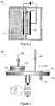
- the figure 2 provides an example of known means that can be used to porously render the surface layer 122 of the original substrate controllable.
- porous silicon electrochemically from monocrystalline silicon Since the fifties it is known to obtain porous silicon electrochemically from monocrystalline silicon.
- the porosification is obtained by anodic dissolution in the presence of hydrofluoric acid (HF).
- An apparatus 200 of the type represented in figure 2 can be used to treat each silicon wafer constituting the first substrate of the process described in figure 1 .
- the face 212 of the substrate 210 to be porosified is brought into contact with an aqueous medium of hydrofluoric acid 240, the concentration of which can typically vary from 1% to 50% and advantageously from 5% to 35%.
- a potential difference or a continuous current is imposed between a cathode 230, immersed in the hydrofluoric acid aqueous solution, and an anode 220 which is in electrical contact with the other face of the substrate to be porosified.
- the hydrofluoric acid concentration of the aqueous medium, the value of the current that is imposed and the anodizing time are, inter alia, parameters which make it possible to control the characteristics of the porous layer that it is desired to obtain. More sophisticated apparatus than that shown also illuminate the aqueous medium adding additional control means of the characteristics of the porous layer.
- the use of an illumination of the aqueous medium depends essentially on the type of porous semiconductor sought and the resistivity thereof.
- the electrolytic solution used (its hydrofluoric acid concentration); current flowing between anode and cathode; the applied voltage; the conditions of illumination as well as the very nature of the substrate (type P, N, its level of doping) intervene to make it possible to control, according to the applications, the obtaining of pores of sizes which can vary in a wide range of values from from a few nanometers to a few micrometers.
- the porosification can be obtained directly, without requiring any other treatment, by anodizing the substrate in the acid medium.
- the current density used to porosity such a material may vary from a few milliAmpere / cm 2 to several amperes / cm 2 .
- the higher the acid concentration the higher the working current densities can be without significant inconvenience. It is thus possible to vary the pore size in the range of values indicated above as well as the porosity rate. The latter can typically range from 10 to 90%.
- a treatment of the back face should be considered to reduce the electrical resistance. This will be done before the porosification step, for example, by ion implantation on the rear face of the first substrate of a P type dopant.
- porous silicon obtained pore sizes, porosity rate and thickness
- concentration of the acid medium, current density, illumination, type of substrate concentration of the acid medium, current density, illumination, type of substrate
- the figure 3 describes the means used during the second stage of chemical mechanical thinning to accurately detect the emergence of the porous silicon layer.
- Chemical mechanical polishing is a technique widely used in the field of microelectronics to polish substrates and to flatten patterns obtained after deposition of thin films. on a substrate.
- the surface is polished by friction on a fabric called "pad” made of porous viscoelastic polyurethane, whose properties (including: hardness, compressibility, shape and size of the pores and patterns) are adapted to the nature of the material to be polished and the smoothness of the polishing to be obtained.
- the material on the surface of the substrate is removed by the combination of the mechanical action resulting from friction on the pad and a chemical reaction with an aqueous solution containing nanoscale particles in suspension called "slurry".
- the chemical solution can be acidic or basic and include abrasive particles of various types and sizes.
- the silicon wafer is placed in an apparatus 300 of the type represented in FIG. figure 3 . It is fixed on the rotary polishing head 320, the face to be polished facing downwards. The whole is supported on the turntable 330 on which is fixed the cloth or polishing pad 340 described above.
- the polishing head exerts a pressure 325 on the silicon wafer.
- the backing force and the relative speed between the head and the plate make it possible to control the speed and the uniformity of the removal of the material.
- the abrasive solution, the slurry is continuously dispensed on the tray with controlled flow. During polishing the abrasive solution is continuously renewed while the polished material suspended therein is discharged to the outside of the plate by centrifugal effect.
- the polishing conditions have been carefully studied by the scientific community working in this field.
- the speed of removal of the material has been modeled and can be estimated with a relatively good accuracy according to all the parameters which control it, in particular: the support pressure, the orbital relative speed of the silicon wafer, the flow rate of the aqueous solution containing the abrasive particles and its composition, the ambient temperature.
- the support pressure the support pressure
- the orbital relative speed of the silicon wafer the flow rate of the aqueous solution containing the abrasive particles and its composition
- the ambient temperature we can refer to an article by D. Peyrade et al., Published in "Microelectronic Engineering 83, p. 1521 »in 2006 .
- the invention is not based on a determination, as precise as it may be, of the removal rate to stop the polishing. It is done automatically on the basis of the detection of the emergence of the porous silicon layer produced on the surface of the first substrate as described in figure 2 . Stop which can be done optionally either at the beginning of detection, at the end of detection, or in the interval, according to which all or part of the porous silicon layer must be removed according to the type of device to be produced.
- the intensity of the signals detected will also depend for many of the physical characteristics of the porous layer 122 which will have been formed on the substrate 110.
- the invention reported in figure 1 a method of forming this layer at low temperature (750 ° C) so that the initial physical characteristics of the underlying porous layer are not substantially affected and remain optimal for its detection.
- the detection means described above, used alone or in combination, however, are sufficiently sensitive to accommodate a change in the physical characteristics of the porous layer which would cause the formation of the monocrystalline layer would cause a weakening of the signal or signals detected.
- the epitaxy can be carried out at a temperature of 950 ° C. It has been shown that if this weakens the detection signals of the porous zone because of the porous layer changes resulting from the use of a heat treatment at temperatures above 750 ° C these remain however sufficiently discernable to precisely control the stopping of mechanical or mechano-chemical polishing.
- the invention is very advantageous on this point by taking advantage of a layer transition detection to stop the thinning.
- Current techniques playing on the selectivity of a chemical attack between porous and non-porous layer could not be implemented at high temperatures, by falling selectivity.
- the figure 4 illustrates more particularly the optical detection mode described above.
- the optical absorption between a porous silicon layer and the dense silicon of the substrate is very different. This difference can be observed by an appropriate optical detection system that can work in a wide range of wavelengths, typically between 800 nm up to and beyond the micrometer, that is, in the red and the infrared. The difference in optical absorption is observable for the wide range of porous silicon considered above and whose characteristics (porosity rate, pore size) can be very different depending on the type of devices to produce.
- An optional improvement of the detection can be implemented which consists in adding a specific product in the abrasive solution (slurry), in particular a "dye”, in order to facilitate the optical detection of the type of layer being polished. This, diffusing into the porous silicon layer, will modify the optical properties and improve the detection of transitions.
- the additive must necessarily be chosen taking into account not only its solubility in the slurry but also according to the optical detection system used and the absorption or reflection properties of the slurry / additive mixture for the wavelength range thereof.
- the additive must also not modify the primary function of the polishing solution and degrade one of the materials in the presence.
- chemical polishing solutions are most often of an aqueous nature, of acid (pH ⁇ 7) or alkaline (pH ⁇ 7) type.
- a number of dyes (or pigments) are actually soluble in water. Companies are specialized in the manufacture of this type of compounds and offer dyes throughout the visible spectrum of colors.
- Curve 400 gives an example of an optical absorption difference which can be observed between the dense silicon of the substrate and that of the porous layer and which makes it possible to very accurately detect the transition 410 between the two types of material.
- the optical absorption shown on the ordinate is the ratio between the intensity of the light emitted on the intensity of that which is reflected, measured here in Lux.
- the figure 5 discloses an alternative embodiment of the invention in which the porous silicon layer that is made during the first step 120 of the method described in figure 1 over the entire surface of the first substrate is replaced by the creation of a plurality of patterns made of porous silicon.
- the patterns are created by adding beforehand to the porosification step by anodic dissolution in the presence of hydrofluoric acid described in figure 2 the following steps which will make it possible to define on the surface of the first substrate, in place of the continuous layer, all the porous silicon zones that one wishes to create.
- the starting point 510 is a monocrystalline silicon substrate.
- a layer of a material 522 will be deposited which will serve as protection during the porosification operation for the surfaces between all the zones to be porosified.
- the deposited material must be resistant to anodic dissolution. This is for example the case of silicon nitride (Si 3 N 4 ).
- the deposition can be achieved by various methods commonly used in microelectronics, for example at relatively low temperature by gaseous means forming a plasma in a confined space.
- the following operations are conventional photolithography operations that make it possible to define the patterns of the zones in which the porosification of the silicon will have to be operated. These operations include the deposition 530 of a resin layer 532. Deposit which is followed by the photolithography operation 540 comprising the dissolution of the resin at the location of the patterns to be etched 542 after it has been selectively insolated at through a mask for example. The etching 550 of the silicon nitride layer is then performed at the locations defined by the patterns 552 after which all the resin is removed.
- the porosification of the silicon is carried out under the same conditions as described in step 120 of the figure 1 and with the means described in figure 2 .
- the difference being in this case that only the areas not protected by silicon nitride 562 are porosified on the surface.
- the next step 570 is to remove the remaining silicon nitride leaving only the porous silicon patterns 572 on the surface of the first substrate.
- porous silicon patterns are present in this case on the surface of the first substrate, instead of a continuous layer of porous silicon, the result is equivalent to that obtained in step 120 of FIG. figure 1 .
- All other steps (130 to 170) can then be applied identically to produce devices from both sides of the same substrate as described in FIG. figure 1 .
- the critical step of automatically stopping polishing in the second thinning step of the first substrate 170 will be similar in that the area covered by the porous silicon patterns is large.
- This variant of the method according to the invention significantly extends the realization options that can be considered for the manufacture of devices from both sides of the same substrate.
- the presence of porous silicon patterns left after the second thinning operation can be revealed and used to position the components to be made on the second face of the substrate with respect to those already created on the first face.
- the invention describes the use of a silicon layer comprising at least one porous zone as a detection layer inside a substrate for the controlled stop of a polishing.
Description
La présente invention concerne la technologie des circuits intégrés en général et décrit plus particulièrement un procédé permettant un contrôle précis de l'amincissement d'un substrat dans le cadre de la réalisation de dispositifs à partir des deux faces dudit substrat.The present invention relates to integrated circuit technology in general and more particularly describes a method allowing precise control of the thinning of a substrate in the context of producing devices from both sides of said substrate.
Si la technologie des circuits intégrés a énormément évoluée depuis leur introduction et leur large déploiement qui a commencé dès le début des années soixante elle est cependant longtemps restée proche, dans son principe, du mode de fabrication initial. Partant d'un substrat, c'est-à-dire d'une tranche très fine tronçonnée dans un lingot fait d'un matériau semi conducteur monocristallin, du silicium essentiellement, toutes les opérations qui permettent la réalisation des circuits intégrés s'effectuent à partir d'une seule des faces du substrat. Face qui a préalablement été soigneusement traitée mécaniquement et/ou chimiquement jusqu'à obtenir un poli de qualité optique. À partir de ce composant de base utilisé par toute l'industrie de la micro électronique, et généralement produit par des fabricants spécialisés, toutes les opérations s'enchaînent pour réaliser, sur la surface polie du substrat, à partir d'une seule des faces donc, les circuits intégrés des plus simples aux plus complexes.While the technology of integrated circuits has evolved enormously since their introduction and their wide deployment that began in the early sixties it has long remained close, in principle, the original mode of manufacture. Starting from a substrate, that is to say a very thin slice cut into an ingot made of a monocrystalline semiconductor material, essentially silicon, all the operations that allow the realization of the integrated circuits take place at from only one of the faces of the substrate. Face that has previously been carefully treated mechanically and / or chemically to obtain an optical grade polish. From this basic component used by the entire microelectronics industry, and usually produced by specialized manufacturers, all the operations are linked to achieve, on the polished surface of the substrate, from a single face therefore, integrated circuits from the simplest to the most complex.
Des techniques telles que : épitaxie, dépôt, gravure, implantation ionique, photolithographie, traitement thermique, polissage mécano chimique, nettoyage/décapage sont couramment utilisées dans la fabrication de composants microélectroniques.Techniques such as: epitaxy, deposition, etching, ion implantation, photolithography, heat treatment, chemical mechanical polishing, cleaning / stripping are commonly used in the manufacture of microelectronic components.
Quoi que les techniques ci-dessus, et en particulier la photo lithographie, aient dû évoluer considérablement au cours des cinq décennies qui ont vu, depuis les années soixante, un accroissement exponentiel jamais démenti de la densité d'intégration des circuits intégrés, la technologie est restée la même en ce que les composants sont toujours formés en surface et à partir d'une seule des faces du substrat.Although the above techniques, and in particular photo lithography, have had to evolve considerably over the five decades since the 1960s, there has been an exponential increase in the integration density of integrated circuits. has remained the same in that the components are always formed on the surface and from only one of the faces of the substrate.
Ce n'est que beaucoup plus récemment que pour, entre autres besoins, celui de pouvoir disposer de composants hybrides performants, par exemple, des composants optoélectroniques tels que des imageurs du type de ceux qui sont utilisés dans les appareils photos et les caméras numériques, dans lesquels fonctions électroniques et optiques sont intimement imbriquées, il est apparu très avantageux de pouvoir réaliser ces composants à partir des deux faces d'un même substrat. Ce qui élargissait considérablement les possibilités de réalisation tout en permettant une grande amélioration de nombre de leurs caractéristiques opérationnelles. Ainsi dans l'exemple ci-dessus d'un imageur, la réalisation des circuits électroniques et leur interconnexion peuvent se faire classiquement sur une face sans interférer avec la réalisation de micro lentilles sur l'autre face et, donc, sans impacter les paramètres optiques du composant.It is only much more recently that for, among other needs, that of having powerful hybrid components, for example, optoelectronic components such as imagers of the type used in cameras and digital cameras, in which electronic and optical functions are intimately interwoven, it appeared very advantageous to be able to make these components from both sides of the same substrate. This considerably broadened the possibilities of realization while allowing a great improvement of many of their operational characteristics. Thus in the above example of an imager, the realization of the electronic circuits and their interconnection can be done conventionally on one side without interfering with the production of micro lenses on the other side and, therefore, without impacting the optical parameters. component.
Il y a bien d'autres exemples dans lesquels la réalisation de dispositifs à partir des deux faces d'un même substrat est très avantageuse incluant les dispositifs hybrides dits NEMS ou MEMS de l'anglais « nano/micro electro mechanical system ».There are many other examples in which the production of devices from both sides of the same substrate is very advantageous including hybrid devices called NEMS or MEMS of the English "nano / micro electro mechanical system".
Pour pouvoir mettre en oeuvre cette façon de faire, le substrat d'origine, après réalisation de tout ou partie des composants sur l'une des faces, doit être transféré sur un support mécanique, un second substrat, afin de pouvoir amincir le premier, à partir de l'autre face, jusqu'à approcher le plus possible tout en la préservant la zone superficielle dans laquelle les premiers composants ont été réalisés. Pour lui donner une solidité mécanique qui permette toutes les manipulations, un substrat doit être en effet relativement très épais en regard de la fine couche superficielle dans laquelle les composants sont réalisés. Son épaisseur initiale n'est cependant pas compatible avec la réalisation de composants performants à partir de la seconde face. Le premier substrat doit donc être aminci après que le second ait été fixé pour prendre le relais d'un point de vue mécanique. L'amincissement du premier substrat doit alors s'effectuer.To be able to implement this way of doing things, the original substrate, after making all or some of the components on one of the faces, must be transferred onto a mechanical support, a second substrate, in order to be able to thin the first, from the other side, to approach as much as possible while preserving the surface area in which the first components were made. To give it a mechanical strength that allows all manipulations, a substrate must indeed be relatively very thick compared to the thin surface layer in which the components are made. Its initial thickness, however, is not compatible with the production of powerful components from the second side. The first substrate must be thinned after the second has been fixed to take over from a mechanical point of view. The thinning of the first substrate must then take place.
L'état de la technique antérieure qui peut être considéré comme utile pour comprendre la divulgation présente est
-
YONEHARA T ET AL: "EPITAXIAL LAYER TRANSFER BY BOND AND ETCH BACK OF POROUS SI",APPLIED PHYSICS LETTERS, AIP, AMERICAN INSTITUTE OF PHYSICS, MELVILLE, NY, US LNKD- DOI:10.1063/1.111698, vol. 64, no. 16, 18 avril 1994 (1994-04-18), pages 2108-2110 -
US 6 054 363 A (SAKAGUCHI KIYOFUMI -
DE 101 00 194 A1
-
YONEHARA T AND AL: "EPITAXIAL LAYER TRANSFER BY BOND AND ETCH BACK OF POROUS SI", APPLIED PHYSICS LETTERS, AIP, AMERICAN INSTITUTE OF PHYSICS, MELVILLE, NY, US LNKD-DOI: 10.1063 / 1.111698, vol. 64, no. 16, April 18, 1994 (1994-04-18), pages 2108-2110 -
US 6,054,363 A (SAKAGUCHI KIYOFUMI -
DE 101 00 194 A1
La difficulté majeure pour mettre en oeuvre cette technique dans le cadre d'un processus industriel reproductible tient au fait qu'il faut pouvoir contrôler très précisément l'arrêt de cet amincissement du premier substrat afin de préserver la mince couche superficielle dans laquelle tout ou partie des composants ont déjà été formés à partir de la première face, et sans les endommager.The major difficulty in implementing this technique in the context of a reproducible industrial process lies in the fact that it is necessary to be able to very precisely control the stopping of this thinning of the first substrate in order to preserve the thin surface layer in which all or part of components have already been formed from the first side, and without damaging them.
C'est donc un objet de l'invention que de décrire un procédé propre à obtenir ce résultat.It is therefore an object of the invention to describe a method suitable for obtaining this result.
Alors que les techniques actuelles proposent une réduction d'épaisseur par rupture ou découpe latérale du substrat dans une zone de faiblesse de son épaisseur (qui peut être poreuse), l'invention préconise un amincissement progressif en plusieurs phases évitant la complexité des méthodes précitées.While current techniques propose a reduction in thickness by rupture or lateral cutting of the substrate in a zone of weakness of its thickness (which can be porous), the invention recommends progressive thinning in several phases avoiding the complexity of the aforementioned methods.
Les autres objets, caractéristiques et avantages de la présente invention apparaîtront à l'examen de la description suivante et des dessins d'accompagnement. Il est entendu que d'autres avantages peuvent être incorporés.Other objects, features and advantages of the present invention will become apparent from the following description and accompanying drawings. It is understood that other benefits may be incorporated.
L'invention répond à ce besoin en décrivant un procédé de fabrication d'un substrat comprenant une étape d'amincissement de l'épaisseur du substrat. Le procédé de fabrication d'un substrat de l'invention présente comprend une étape d'amincissement de l'épaisseur du substrat, caractérisé par le fait qu'il comporte les étapes suivantes:
- formation d'une zone poreuse dans une couche intérieure du substrat ;
- amincissement progressif de l'épaisseur du substrat en direction de la couche intérieure comprenant la zone poreuse ;
- finalisation de l'amincissement progressif par polissage mécano chimique ;
- arrêt automatique contrôlé du polissage par détection de la zone poreuse au cours du polissage.
- forming a porous zone in an inner layer of the substrate;
- progressively thinning the thickness of the substrate towards the inner layer comprising the porous zone;
- finalization of progressive thinning by chemical mechanical polishing;
- controlled automatic stop of polishing by detection of the porous zone during polishing.
Le procédé comprend en outre les étapes et caractéristiques optionnelles suivantes :
- La zone poreuse forme l'intégralité de la couche intérieure.
- La zone poreuse comporte une pluralité de portions poreuses dans la couche intérieure.
- La formation de la zone poreuse est effectuée par porosification d'une épaisseur prédéterminée de la surface d'un substrat primaire suivie par le dépôt ou la croissance d'au moins une couche de recouvrement d'un matériau participant à la réalisation d'un dispositif électronique ou d'un dispositif hybride incluant une partie optique et/ou mécanique.
- La croissance d'au moins une couche de recouvrement est opérée par épitaxie à une température supérieure à 750° C.
- La température est comprise entre 900°C et 1100°C.
- Le dépôt ou la croissance de la au moins une couche de recouvrement est suivi d'un report sur un substrat secondaire fixé sur la dernière des au moins une couche de recouvrement.
- L'étape d'amincissement progressif du substrat est plus rapide que la phase de finalisation de l'amincissement.
- La première phase d'amincissement est effectuée par attaque chimique ou par abrasion mécanique ou par polissage mécano chimique (CMP).
- L'arrêt contrôlé du polissage est opéré immédiatement à la détection de la zone poreuse.
- L'arrêt contrôlé du polissage est opéré après un temps programmé après la détection de la zone poreuse.
- La détection de la zone poreuse est une détection de transition entre une zone non poreuse et la zone poreuse.
- La détection de transition est opérée lors du passage d'une zone non poreuse à la zone poreuse au cours de la finalisation.
- La détection de transition est opérée lors du passage de la zone poreuse à une zone non poreuse au cours de la finalisation.
- La finalisation de l'amincissement progressif par polissage comprend :
- une étape préliminaire de finalisation,
- un arrêt contrôlé de l'étape préliminaire de finalisation par détection d'une transition depuis une zone non poreuse du substrat vers la zone poreuse,
- une étape secondaire de finalisation jusqu'à l'arrêt contrôlé du polissage.
- L'étape secondaire est opérée à vitesse plus lente que l'étape préliminaire.
- On détecte la zone poreuse en exposant la surface en cours de polissage à une source lumineuse et en surveillant l'absorption et/ou la réflexion optique de la surface pour déterminer un début et/ou une fin d'attaque de la couche poreuse.
- La surveillance de l'absorption et/ou de la réflexion optique est améliorée en introduisant dans la solution abrasive un additif destiné à diffuser dans la zone poreuse.
- L'additif est un colorant dont la couleur est complémentaire de la gamme de longueurs d'ondes détectable par le système surveillant l'absorption et/ou la réflexion optique de la surface en cours de polissage.
- On détecte la zone poreuse en mesurant le couple moteur entre la tête et le plateau de polissage pour déterminer les changements de friction indiquant un début et/ou une fin d'attaque de la couche poreuse.
- On détecte la zone poreuse en mesurant l'échauffement du substrat pour déterminer les changements de température indiquant un début et/ou une fin d'attaque de la couche poreuse.
- The porous zone forms the entire inner layer.
- The porous zone has a plurality of porous portions in the inner layer.
- The formation of the porous zone is effected by porosifying a predetermined thickness of the surface of a primary substrate followed by the deposition or growth of at least one covering layer of a material involved in the production of a device. electronic or hybrid device including an optical and / or mechanical part.
- The growth of at least one covering layer is effected by epitaxy at a temperature above 750 ° C.
- The temperature is between 900 ° C and 1100 ° C.
- The deposition or the growth of the at least one covering layer is followed by a transfer on a secondary substrate fixed on the last of the at least one covering layer.
- The stage of progressive thinning of the substrate is faster than the phase of finalization of the thinning.
- The first phase of thinning is performed by etching or mechanical abrasion or chemical mechanical polishing (CMP).
- The controlled stop of the polishing is carried out immediately on detection of the porous zone.
- The controlled stop of the polishing is operated after a programmed time after the detection of the porous zone.
- The detection of the porous zone is a transition detection between a non-porous zone and the porous zone.
- Transition detection is performed when moving from a non-porous area to the porous area during finalization.
- Transition detection is performed when the porous zone is moved to a non-porous zone during finalization.
- The finalization of progressive thinning by polishing comprises:
- a preliminary stage of finalization,
- a controlled stop of the preliminary finalization step by detecting a transition from a non-porous zone of the substrate to the porous zone,
- a secondary step of finalization until the controlled stop of the polishing.
- The secondary stage is operated at a slower speed than the preliminary stage.
- The porous area is detected by exposing the surface being polished to a light source and monitoring the absorption and / or optical reflection of the surface to determine a start and / or end of etching of the porous layer.
- The monitoring of the absorption and / or optical reflection is improved by introducing into the abrasive solution an additive intended to diffuse into the porous zone.
- The additive is a dye whose color is complementary to the range of wavelengths detectable by the system monitoring the absorption and / or optical reflection of the surface being polished.
- The porous zone is detected by measuring the motor torque between the head and the polishing plate to determine the friction changes indicating a start and / or end of etching of the porous layer.
- The porous zone is detected by measuring the heating of the substrate to determine the temperature changes indicating onset and / or end of etching of the porous layer.
L'invention décrit l'utilisation d'une couche de matériau semi conducteur tel du silicium comportant au moins une zone poreuse comme couche de détection à l'intérieur d'un substrat pour l'arrêt contrôlé d'un polissage.The invention describes the use of a layer of semiconductor material such as silicon having at least one porous zone as a detection layer inside a substrate for the controlled stop of a polishing.
L'invention décrit en outre un procédé dans lequel la pluralité de portions poreuses dans la couche intérieure est révélée à l'issue de la phase de finalisation contrôlée de l'amincissement pour permettre l'alignement de la partie des dispositifs fabriquée à partir d'une seconde face du substrat sur celle déjà fabriquée à partir d'une première face du substrat.The invention furthermore describes a method in which the plurality of porous portions in the inner layer are revealed at the conclusion of the controlled thinning finalization phase to allow alignment of the portion of the devices made from a second face of the substrate on that already manufactured from a first face of the substrate.
Les buts, objets, ainsi que les caractéristiques et avantages de l'invention ressortiront mieux de la description détaillée d'un mode de réalisation de cette dernière qui est illustré par les dessins d'accompagnement suivants dans lesquels :
- La
FIGURE 1 décrit les différentes étapes du procédé selon l'invention. - La
FIGURE 2 donne un exemple de moyen connu qui peut être utilisé pour rendre poreux d'une façon contrôlée la couche superficielle du substrat d'origine. - La
FIGURE 3 décrit les moyens mis en oeuvre lors de la deuxième étape d'amincissement mécano chimique pour détecter précisément l'émergence de la couche de silicium poreux. - La
FIGURE 4 illustre plus particulièrement le mode de détection optique qui sert à détecter l'émergence de la couche de silicium poreux. - La
FIGURE 5 décrit une variante de mise en oeuvre de l'invention dans laquelle la couche continue de silicium poreux est remplacée par la création d'une pluralité de motifs faits de silicium poreux.
- The
FIGURE 1 describes the different steps of the method according to the invention. - The
FIGURE 2 provides an example of known means that can be used to porously render the surface layer of the original substrate porous. - The
FIGURE 3 describes the means used during the second stage of chemical mechanical thinning to accurately detect the emergence of the porous silicon layer. - The
FIGURE 4 illustrates more particularly the optical detection mode which serves to detect the emergence of the porous silicon layer. - The
FIGURE 5 discloses an alternative embodiment of the invention in which the continuous layer of porous silicon is replaced by the creation of a plurality of patterns made of porous silicon.
Les dessins joints sont donnés à titre d'exemples et ne sont pas limitatifs de l'invention.The accompanying drawings are given by way of example and are not limiting of the invention.
La
Comme déjà indiqué dans le chapitre sur l'état de la technique un matériau de base de toute l'industrie des semi conducteurs et de la micro électronique est communément un substrat monocristallin de silicium 110, souvent dopé de type P, et dont une des faces a déjà reçu généralement un poli optique. Son épaisseur est suffisante pour donner au substrat une solidité et une rigidité mécanique qui permettent toutes les manipulations lors des très nombreuses étapes de fabrication nécessaires à la réalisation de circuits intégrés à sa surface. Substrat qui se présente sous la forme d'une tranche mince dont le diamètre atteint actuellement 30 centimètres et à la surface duquel on réalise simultanément, en fonction de leurs tailles, typiquement, quelques centaines de circuits intégrés simultanément. Si, comme mentionné ci-dessus, le substrat est généralement fait de silicium, l'invention ne fait cependant aucune hypothèse sur la nature de ce dernier hormis le fait qu'il doit pouvoir être porosifié en surface. Notamment, l'utilisation d'autres types de substrats semi-conducteurs tels que le germanium, ou des alliages silicium/germanium (SiGe) peut aussi être considéré comme rapporté, par exemple, dans la publication suivante :
Des alliages semi conducteurs binaires du type III-V conviennent également pour l'invention. Il s'agit notamment de l'arséniure de gallium (AsGa), du phosphure d'indium (InP) ou du nitrure de gallium (GaN).Binary semiconductor alloys of the III-V type are also suitable for the invention. These include gallium arsenide (AsGa), indium phosphide (InP) or gallium nitride (GaN).
Le procédé selon l'invention demande que dans une première étape 120 une porosification d'une couche superficielle 122 du substrat soit effectuée. D'une façon générale tout matériau cristallin, semi conducteur comme ceux mentionnés ci-dessus, ou non, ou d'un alliage de tels matériaux, pouvant être porosifié est donc susceptible de constituer le substrat 110 à partir duquel le procédé de l'invention sera appliqué. En ce qui concerne le silicium par exemple, la porosification consiste à mettre en oeuvre des techniques connues depuis les années cinquante. Des exemples de mise en oeuvre sont donnés en
On notera par ailleurs que les substrats de silicium sont généralement produits avec une orientation cristalline notée (100). Pour certaines applications il peut être avantageux d'utiliser un substrat en silicium ayant été produit avec une orientation cristalline différente comme par exemple : (111), (110) ou autre. L'obtention de la couche de silicium poreux décrite en
L'étape suivante 130 consiste à former par-dessus la couche poreuse 122 la ou les couches 132 dans lesquelles les composants seront créés. L'invention ne fait pas d'hypothèse sur le type de composants dont la fabrication est susceptible de bénéficier du procédé décrit. La couche globale 132 pourra elle-même comprendre une pluralité de couches faites de différents matériaux incluant par exemple le silicium sous ses différentes formes : monocristallin, polycristallin, amorphe ; et d'une façon générale tous les matériaux et alliages semi conducteurs mentionnés plus hauts. La couche globale 132 pourra comprendre en outre des oxydes pouvant servir de diélectrique et incluant l'oxyde de silicium ; et d'une façon générale tous les matériaux couramment utilisés par l'industrie de la microélectronique et incluant des dépôts sous vide de couches métalliques d'aluminium, de cuivre, d'or ou d'argent. La formation de la couche globale 132 pourra être obtenue par tous les moyens couramment utilisés pour faire croître ou déposer des matériaux sur un substrat.The
Dans l'exemple précédemment mentionné de dispositifs optoélectroniques de type imageur, et d'une façon générale de tout dispositif électronique élaboré devant inclure des éléments actifs de type transistors, la couche 132 sera alors avantageusement formée en faisant croître une couche monocristalline par épitaxie directement sur la couche poreuse 122. La couche porosifiée conservant la structure cristalline du substrat dans lequel elle a été formée tous les types de croissance épitaxiale connus peuvent être envisagés lors de la mise en oeuvre de l'invention.In the previously mentioned example of optoelectronic devices of the imager type, and in general of any elaborated electronic device to include transistor-type active elements, the
Le plus couramment une homo-épitaxie de type silicium sur silicium sera pratiquée. Pour tous les autres types de substrats discutés ci-dessus une homo-épitaxie est aussi possible. Il s'agira par exemple d'une épitaxie de SiGe sur une couche ou un substrat de SiGe ou d'une épitaxie d'AsGa sur une couche ou un substrat d'AsGa. Plus généralement, une hétéro-épitaxie d'un matériau X peut être envisagée sur un substrat porosifié Y dans la mesure où la structure cristalline des matériaux X et Y permet que la croissance épitaxiale puisse se faire harmonieusement. Par exemple, sur un substrat de silicium orienté (100), un dépôt de Si(C), solution solide jusqu'à 1% de Carbone, du Ge, du SiGe, de l'AsGa et plus généralement les alliages semi conducteurs de type III-V peuvent être épitaxiés. Sur un substrat de silicium orienté (111) ou (100) un film de SiC, composé intermétallique de silicium et de carbone, peut aussi être épitaxié.Most commonly silicon-on-silicon homo-epitaxy will be practiced. For all other types of substrates discussed above homoepitaxy is also possible. This will be for example a SiGe epitaxy on a SiGe layer or substrate or an AsGa epitaxy on an AsGa layer or substrate. More generally, a hetero-epitaxy of a material X can be envisaged on a porosized substrate Y insofar as the crystalline structure of materials X and Y allows the epitaxial growth to be harmonious. For example, on an oriented silicon substrate (100), a deposit of Si (C), solid solution up to 1% of carbon, Ge, SiGe, AsGa and more generally semiconductor alloys of the type III-V can be epitaxially grown. On an oriented silicon substrate (111) or (100) an SiC film, an intermetallic silicon and carbon compound, may also be epitaxially grown.
Il est en particulier bien connu de pouvoir épitaxier une couche de silicium monocristalline de bonne qualité sur du silicium poreux. Les conditions d'épitaxie peuvent avoir à différer de celles communément utilisées sur silicium massif si on ne veut pas modifier la structure du silicium poreux qui a été précédemment formé. En particulier, une fois le silicium poreux réalisé, un premier traitement thermique sous vide pourra être appliqué afin de stabiliser la morphologie du silicium poreux avant de réaliser une épitaxie dite à basse température (750°C). Sur ce sujet on pourra par exemple se reporter à la publication suivante :
Dans cet exemple de fabrication de dispositifs optoélectroniques ou dans des dispositifs élaborés comprenant des composants actifs de type transistor toute la partie électronique des dispositifs sera ensuite réalisée d'une façon traditionnelle dans la couche monocristalline épitaxiale 132. Cela comprendra, par exemple, la formation de circuits faits de transistors CMOS (de l'anglais « complementary metal oxide semiconductor ») en faisant appel aux techniques standard mentionnées dans le chapitre sur l'état de la technique : oxydation, photolithographie, diffusion, implantation, dépôt métallique, formation des interconnexions, etc.In this example of fabrication of optoelectronic devices or in elaborate devices comprising active components of the transistor type, the entire electronic part of the devices will then be produced in a conventional manner in the epitaxial
Quand la partie des dispositifs qui doit être fabriquée à partir de la première des faces du substrat d'origine est terminée, il faut alors fixer ce dernier, à l'étape suivante 140, sur un second substrat 142 pour réaliser le transfert de la couche 132 et ainsi permettre l'achèvement de la partie des dispositifs qui se fera à partir de la seconde face après amincissement du substrat d'origine. La fixation du second substrat se fait à l'aide de méthodes et de techniques connues permettant d'empiler au niveau tranche des substrats dont les circuits sont partiellement ou entièrement fabriqués. Notamment, on peut faire appel à une technique de collage par adhésion moléculaire oxyde sur oxyde à basse température. Le silicium poreux peut supporter des températures allant jusqu'à 750°C sans entraîner de modifications sensibles de ses caractéristiques physiques. Les collages moléculaires peuvent se faire efficacement jusqu'à ces températures. Ce type de fixation pourra nécessiter le dépôt préalable d'une couche protectrice et une préparation de la surface des substrats 144. L'invention ne fait pas d'hypothèse sur la nature du second substrat 142 dont le rôle est essentiellement de constituer un support mécanique pour les opérations suivantes.When the portion of the devices that is to be manufactured from the first of the faces of the original substrate is completed, it is then necessary to fix the latter, in the
Le résultat est un assemblage 150 au niveau tranche de deux substrats dont le premier 152, celui d'origine, doit être aminci. Par commodité, la représentation de l'assemblage 150 est retournée pour que la face supérieure représente la seconde face du premier substrat, celle à partir de laquelle on va finir de réaliser les dispositifs en cours de fabrication après amincissement.The result is an
Dans un mode préféré de mise en oeuvre de l'invention, l'amincissement se fait en au moins deux étapes :
- Au cours d'une première étape 160 on réalise un retrait rapide du silicium qui puisse cependant garantir que la couche de silicium poreux 122, et donc la couche contenant les dispositifs 132, ne soient en aucun cas touchées. Par exemple, la majeure partie du silicium peut être retirée par abrasion mécanique ou par voix chimique ou en combinant les deux moyens. L'attaque chimique peut se faire en utilisant des produits tels que l'hydroxyde de tetramethylammonium (TMAH), l'hydroxyde de potassium ou potasse (KOH), ou encore l'hydroxyde de potassium ou soude (NaOH). Cette première étape préserve donc une partie du silicium d'origine, la couche de silicium poreux et celle contenant les dispositifs en cours de
fabrication 162. A l'issue de ce retrait rapide l'état desurface 164 peut alors être relativement mauvais. - La seconde étape de l'amincissement dite de finalisation consiste à améliorer l'état de surface à l'aide d'un polissage mécano chimique jusqu'à obtenir un nivellement et un état de
surface 172 compatible avec les dispositifs à fabriquer. La seconde étape 170 est cruciale en ce que l'amincissement supplémentaire obtenu doit être détecté très précisément pour s'arrêter dès que l'on rencontre le silicium poreux, si cette couche participe à la fabrication du dispositif, ou exactement à l'interface entre silicium poreux et la couche 132 contenant la partie des composants qui ont été réalisés à partir de la première face du substrat d'origine si, comme représenté, elle doit être complètement enlevée. Dans le cas où on ôte totalement la couche poreuse, il peut être avantageux de tirer profit de la détection de deux transitions avec la couche poreuse, à savoir une détection, première chronologiquement, de transition du substrat vers la couche poreuse et une détection, deuxième chronologiquement, de transition en sortie de la couche poreuse. Par exemple, une première phase de finalisation d'amincissement est opérée, avec des paramètres de polissage (tels que vitesse, actifs chimiques) données jusqu'à la première détection, et une deuxième phase de finalisation d'amincissement est opérée, avec d'autres paramètres de polissage (par exemple moins rapides et/ou sans attaque chimique) jusqu'à la deuxième détection. Eventuellement, après la deuxième détection, une étape de finition, telle que par polissage CMP, peut être opérée pour laisser un état de surface de qualité améliorée. C'est le rôle premier de la couche de silicium poreux que de permettre la détection. Comme expliqué enfigure 3 différents paramètres lors du polissage mécano chimique peuvent être surveillés permettant une détection précise du début et de la fin de la couche de silicium poreux 122 et donc un arrêt programmé du polissage. Ainsi, la couche de silicium poreux peut être une couche dite « sacrificielle » qui disparaîtra complètement ou, en fonction des dispositifs à produire, participer à la fabrication des dispositifs auquel cas l'arrêt du polissage se fera dès que celle-ci est détectée ou après un temps supplémentaire programmé pour n'en laisser qu'une partie.
- During a
first step 160, a rapid silicon removal is achieved which can however guarantee that theporous silicon layer 122, and therefore the layer containing thedevices 132, are in no way affected. For example, most of the silicon can be removed by mechanical abrasion or chemical voice or by combining the two means. Chemical attack can be done using products such as tetramethylammonium hydroxide (TMAH), potassium hydroxide or potassium hydroxide (KOH), or potassium hydroxide or sodium hydroxide (NaOH). This first step thus preserves part of the original silicon, the porous silicon layer and the one containing the devices inprocess 162. At the end of this rapid withdrawal, thesurface state 164 can then be relatively bad. - The second step of so-called finalization thinning is to improve the surface state using a chemical mechanical polishing until a leveling and a
surface condition 172 compatible with the devices to be manufactured. Thesecond step 170 is crucial in that the additional thinning obtained must be detected very precisely to stop as soon as we meet the porous silicon, if this layer participates in the manufacture of the device, or exactly at the interface between porous silicon and thelayer 132 containing the portion of the components that have been made from the first face of the original substrate if, as shown, it must be completely removed. In the case where the porous layer is completely removed, it may be advantageous to take advantage of the detection of two transitions with the porous layer, namely a first chronological detection of the transition from the substrate to the porous layer and a second detection. chronologically, transition at the outlet of the porous layer. For example, a first thinning finalization phase is carried out, with polishing parameters (such as speed, chemical actives) given until the first detection, and a second phase of thinning completion is performed, with other polishing parameters (for example less rapid and / or without chemical etching) until the second detection. Optionally, after the second detection, a finishing step, such as by CMP polishing, can be performed to leave a surface condition of improved quality. It is the primary role of the porous silicon layer to enable detection. As explained infigure 3 different parameters during the chemical mechanical polishing can be monitored allowing accurate detection of the beginning and the end of theporous silicon layer 122 and thus a programmed stop of the polishing. Thus, the porous silicon layer may be a so-called "sacrificial" layer which will disappear completely or, depending on the devices to be produce, participate in the manufacture of devices in which case stop the polishing will be done as soon as it is detected or after an additional time programmed to leave only a part.
La
Depuis les années cinquante on sait obtenir du silicium poreux par voie électrochimique à partir de silicium monocristallin. La porosification est obtenue par dissolution anodique en présence d'acide fluorhydrique (HF). Un appareillage 200 du type de celui représenté en
Toutes les conditions d'élaboration de la couche poreuse, c'est-à-dire : la solution électrolytique employée (sa concentration en acide fluorhydrique) ; le courant circulant entre anode et cathode ; la tension appliquée ; les conditions d'illumination ainsi que la nature même du substrat (type P, N, son niveau de dopage) interviennent pour permettre de contrôler, en fonction des applications, l'obtention de pores de tailles pouvant varier dans une large plage de valeurs allant de quelques nanomètres à quelques micromètres.All the conditions for producing the porous layer, that is to say: the electrolytic solution used (its hydrofluoric acid concentration); current flowing between anode and cathode; the applied voltage; the conditions of illumination as well as the very nature of the substrate (type P, N, its level of doping) intervene to make it possible to control, according to the applications, the obtaining of pores of sizes which can vary in a wide range of values from from a few nanometers to a few micrometers.
Par exemple, pour un substrat de type P+ dont la résistivité est de l'ordre de quelques dizaines de milliOhms/cm, la porosification peut être obtenue directement, sans nécessiter d'autre traitement, par anodisation du substrat dans le milieu acide. La densité de courant utilisée pour porosifier un tel matériau pourra varier de quelques milliAmpère/cm2 à plusieurs Ampères/cm2. D'une façon générale, plus la concentration en acide est élevée, plus les densités de courant de travail peuvent être sans inconvénient importantes. Il est ainsi possible de faire varier la grosseur des pores dans la plage de valeurs indiquée ci-dessus ainsi que le taux de porosité. Ce dernier pouvant aller typiquement de 10 à 90%.For example, for a P + type substrate whose resistivity is of the order of a few tens of milliOhms / cm, the porosification can be obtained directly, without requiring any other treatment, by anodizing the substrate in the acid medium. The current density used to porosity such a material may vary from a few milliAmpere / cm 2 to several amperes / cm 2 . In general, the higher the acid concentration, the higher the working current densities can be without significant inconvenience. It is thus possible to vary the pore size in the range of values indicated above as well as the porosity rate. The latter can typically range from 10 to 90%.
Dans le cas d'utilisation d'un substrat beaucoup plus résistant, par exemple un substrat de type P ayant une résistivité de plusieurs Ohms/cm, un traitement de la face arrière devra être envisagé pour diminuer la résistance électrique. Cela se fera préalablement à l'étape de porosification, par exemple, par implantation ionique sur la face arrière du premier substrat d'un dopant de type P.In the case of using a much stronger substrate, for example a P-type substrate having a resistivity of several Ohms / cm, a treatment of the back face should be considered to reduce the electrical resistance. This will be done before the porosification step, for example, by ion implantation on the rear face of the first substrate of a P type dopant.
Les caractéristiques morphologiques du silicium poreux obtenu (tailles de pores, taux de porosité et épaisseur) en fonction des conditions mises en oeuvre pour son élaboration et mentionnées ci-dessus (concentration du milieu acide, densité de courant, illumination, type de substrat) sont décrites dans de nombreuses publications scientifiques et ont fait l'objet d'ouvrages dédiés. Ils permettent à l'homme du métier de déterminer rapidement les conditions à mettre en oeuvre pour obtenir, sur un substrat d'un type donné, une couche de silicium poreux de caractéristiques appropriées au type de dispositif à produire.The morphological characteristics of the porous silicon obtained (pore sizes, porosity rate and thickness) as a function of the conditions used for its elaboration and mentioned above (concentration of the acid medium, current density, illumination, type of substrate) are described in numerous scientific publications and have been the subject of dedicated works. They allow those skilled in the art to quickly determine the conditions to be used to obtain, on a substrate of a given type, a porous silicon layer of characteristics appropriate to the type of device to be produced.
La
Le polissage mécano chimique, souvent désigné par l'acronyme CMP (de l'anglais « Chemical Mechanical Polishing »), est une technique largement utilisée dans le domaine de la microélectronique pour polir les substrats et pour aplanir des motifs obtenus après dépôt de couches minces sur un substrat. La surface est polie par frottement sur un tissu appelé « pad » fait de polyuréthane poreux viscoélastique, dont les propriétés (incluant : dureté, compressibilité, forme et dimension des pores et des motifs) sont adaptées à la nature du matériau à polir et à la finesse du polissage à obtenir. Le matériau à la surface du substrat est enlevé par la combinaison de l'action mécanique résultant du frottement sur le pad et d'une réaction chimique avec une solution aqueuse contenant des particules nanométriques en suspension appelée «slurry ». Selon les applications considérées la solution chimique est différente, elle peut être acide ou basique et comprendre des particules abrasives de types et de tailles variés.Chemical mechanical polishing, often referred to as Chemical Mechanical Polishing (CMP), is a technique widely used in the field of microelectronics to polish substrates and to flatten patterns obtained after deposition of thin films. on a substrate. The surface is polished by friction on a fabric called "pad" made of porous viscoelastic polyurethane, whose properties (including: hardness, compressibility, shape and size of the pores and patterns) are adapted to the nature of the material to be polished and the smoothness of the polishing to be obtained. The material on the surface of the substrate is removed by the combination of the mechanical action resulting from friction on the pad and a chemical reaction with an aqueous solution containing nanoscale particles in suspension called "slurry". Depending on the applications considered the chemical solution is different, it can be acidic or basic and include abrasive particles of various types and sizes.
Pour procéder au polissage mécano chimique la tranche de silicium est placée dans un appareillage 300 du type de celui représenté en
Dans le cadre général de l'utilisation de ce type de polisseuse les conditions de polissage ont été étudiées avec soin par la communauté scientifique travaillant dans ce domaine. Notamment, la vitesse d'enlèvement du matériau a été modélisée et peut être estimée avec une relative bonne précision en fonction de tous les paramètres qui la contrôlent, notamment : la pression d'appui, la vitesse relative orbitale de la tranche de silicium, le débit de la solution aqueuse contenant les particules abrasives et sa composition, la température ambiante. On pourra par exemple se reporter à un article par
Toutefois, l'invention ne repose en rien sur une détermination, aussi précise puisse-t-elle être, de la vitesse d'enlèvement pour arrêter le polissage. Il se fait automatiquement sur la base de la détection de l'émergence de la couche de silicium poreux réalisé à la surface du premier substrat comme décrit en
D'une façon générale, dans le cadre d'un polissage mécano chimique, tout paramètre physique mesurable qui admet une variation notable lors d'une transition entre deux couches peut être utilisé comme moyen de détection. L'invention considère plus particulièrement les moyens suivants, utilisés seuls ou en combinaison, pour détecter l'émergence de la couche de silicium poreux au cours de l'opération de polissage mécano chimique.
- Le frottement de la
tranche 310 sur lepad 340 provoque un échauffement qui est différent entre le silicium dense du substrat et celui de la couche poreuse. La mesure de la température peut être surveillée pour détecter les changements de celle-ci et donc les transitions entre couches de natures différentes. - Le polissage doit se faire avec une vitesse constante de rotation du
plateau 330. Afin de garder cette vitesse constante, un asservissement réajuste l'alimentation en courant du moteur 360. Plus la friction est importante, plus le couple moteur doit être fort et plus le courant d'alimentation de ce dernier est élevé. La lecture du courant d'alimentation du moteur 365 permet de détecter la transition entre deux couches d'autant plus facilement qu'elles ont une viscosité fort différente. Ce qui est le cas entre le silicium poreux de surface et le silicium dense du substrat. - Les propriétés optiques de la surface varient beaucoup en cours de polissage en fonction des matériaux rencontrés : silicium dense et poreux dans le cas de l'invention. En ménageant une fenêtre d'observation 370 à travers le plateau et le pad il est possible d'insérer un système de détection optique 375 qui pourra mesurer certaines de ces propriétés, par exemple l'absorption et la réflexion de lumière émise par le système de détection à chaque fois que la tranche en cours de polissage se trouve au dessus de la fenêtre d'observation. En fonction des applications considérées la gamme de longueur d'ondes utilisée peut varier entre celle des rayons dits X (une dizaine de nanomètres) à celle de l'infrarouge (au-delà de 800 nanomètres). Comme avec la température de la tranche et le courant d'alimentation du moteur ces paramètres optiques peuvent être surveillés pour déterminer avec une grande précision les transitions entre couches.
- The friction of the
wafer 310 on thepad 340 causes a heating which is different between the dense silicon of the substrate and that of the porous layer. The measurement of the temperature can be monitored to detect the changes thereof and thus the transitions between layers of different natures. - The polishing must be done with a constant speed of rotation of the
plate 330. In order to keep this speed constant, a servocontrol readjusts the current supply of the motor 360. The greater the friction, the higher the motor torque must be, and the greater the feed current of the latter is high. The reading of the motor supply current 365 makes it possible to detect the transition between two layers all the more easily as they have a very different viscosity. This is the case between the surface porous silicon and the dense silicon of the substrate. - The optical properties of the surface vary a lot during polishing depending on the materials encountered: dense and porous silicon in the case of the invention. By providing an
observation window 370 through the plate and the pad, it is possible to insert anoptical detection system 375 which will be able to measure some of these properties, for example the absorption and the reflection of light emitted by the radiation system. detection whenever the slice being polished is above the observation window. Depending on the applications considered, the range of wavelengths used may vary between that of so-called X-rays (about ten nanometers) and that of the infrared (beyond 800 nanometers). As with the temperature From the wafer and the motor supply current these optical parameters can be monitored to accurately determine the transitions between layers.
À ce stade de la description du procédé de l'invention il convient de remarquer que, quel que soit le ou les moyens mis en oeuvre pour détecter l'émergence de la couche poreuse, l'intensité des signaux détectés (température et/ou frottement et/ou absorption optique) dépendra aussi pour beaucoup des caractéristiques physiques de la couche poreuse 122 qui aura été formée sur le substrat 110. A cet effet, dans le cas où une couche épitaxiale monocristalline doit être formée sur la couche poreuse, l'invention fait état en
On notera que l'invention est sur ce point très avantageuse en tirant profit d'une détection de transition de couches pour arrêter l'amincissement. Des techniques actuelles jouant sur la sélectivité d'une attaque chimique entre couche poreuse et non poreuse ne pourraient être mises en oeuvre aux températures élevées, par chute de la sélectivité.It should be noted that the invention is very advantageous on this point by taking advantage of a layer transition detection to stop the thinning. Current techniques playing on the selectivity of a chemical attack between porous and non-porous layer could not be implemented at high temperatures, by falling selectivity.
La
L'absorption optique entre une couche de silicium poreux et le silicium dense du substrat est très différente. Cette différence peut être observée par un système de détection optique approprié pouvant travailler dans une large gamme de longueur d'onde comprise, typiquement, entre 800 nm jusqu'au micromètre et au-delà, c'est-à-dire dans le rouge et l'infra rouge. La différence d'absorption optique est observable pour la large gamme de silicium poreux considérée précédemment et dont les caractéristiques (taux de porosité, taille des pores) peuvent être très différentes en fonction du type de dispositifs à produire.The optical absorption between a porous silicon layer and the dense silicon of the substrate is very different. This difference can be observed by an appropriate optical detection system that can work in a wide range of wavelengths, typically between 800 nm up to and beyond the micrometer, that is, in the red and the infrared. The difference in optical absorption is observable for the wide range of porous silicon considered above and whose characteristics (porosity rate, pore size) can be very different depending on the type of devices to produce.
Une amélioration optionnelle de la détection peut être mis en oeuvre qui consiste à ajouter un produit spécifique dans la solution abrasive (slurry), notamment un « colorant », afin de faciliter la détection optique du type de couche en cours de polissage. Celui-ci, en diffusant dans la couche de silicium poreux, en modifiera les propriétés optiques et améliorera la détection des transitions.An optional improvement of the detection can be implemented which consists in adding a specific product in the abrasive solution (slurry), in particular a "dye", in order to facilitate the optical detection of the type of layer being polished. This, diffusing into the porous silicon layer, will modify the optical properties and improve the detection of transitions.
S'il s'avère nécessaire d'ajouter un colorant (ou pigment), et plus généralement d'introduire un additif dans la solution de polissage mécano chimique ou slurry, l'additif devra nécessairement être choisi en tenant compte non seulement de sa solubilité dans le slurry mais aussi en fonction du système de détection optique utilisé et des propriétés d'absorption ou de réflexion du mélange slurry/additif pour la gamme de longueur d'ondes de ce dernier. L'additif ne devra pas non plus modifier la fonction première de la solution de polissage et dégrader l'un des matériaux en présence. De façon générale, les solutions chimiques de polissage sont le plus souvent de nature aqueuse, de type acide (pH ≤ 7) ou alcaline (pH ≥ 7). Un certain nombre de colorants (ou pigments) sont effectivement solubles dans l'eau. Des sociétés sont spécialisées dans la fabrication de ce type de composés et proposent des colorants dans toute la gamme du spectre visible des couleurs.If it is necessary to add a dye (or pigment), and more generally to introduce an additive into the chemical mechanical polishing solution or slurry, the additive must necessarily be chosen taking into account not only its solubility in the slurry but also according to the optical detection system used and the absorption or reflection properties of the slurry / additive mixture for the wavelength range thereof. The additive must also not modify the primary function of the polishing solution and degrade one of the materials in the presence. In general, chemical polishing solutions are most often of an aqueous nature, of acid (pH ≤ 7) or alkaline (pH ≥ 7) type. A number of dyes (or pigments) are actually soluble in water. Companies are specialized in the manufacture of this type of compounds and offer dyes throughout the visible spectrum of colors.
De nombreuses publications techniques sont par ailleurs disponibles qui permettent à l'homme du métier de choisir judicieusement l'additif en fonction des caractéristiques du système optique utilisé. Notamment, en considérant la propriété physico-chimique suivante : une solution colorée absorbe la lumière dans la gamme spectrale complémentaire de celle qu'elle émet. En conséquence, si par exemple la longueur d'onde du détecteur est dans le rouge ou proche infra rouge (longueurs d'ondes de l'ordre de 800 à 1000 nm), un colorant vert (longueur d'onde de l'ordre de 550 nm) ou bleu (longueur d'onde de l'ordre de 400nm) sera le plus approprié.Many technical publications are also available which allow the skilled person to choose wisely additive based on the characteristics of the optical system used. In particular, considering the following physico-chemical property: a colored solution absorbs light in the spectral range complementary to that which it emits. Consequently, if for example the wavelength of the detector is in the red or near infrared (wavelengths of the order of 800 to 1000 nm), a green dye (wavelength of the order of 550 nm) or blue (wavelength of the order of 400 nm) will be most appropriate.
La courbe 400 donne un exemple de différence d'absorption optique qui peut être observée entre le silicium dense du substrat et celui de la couche poreuse et qui permet de détecter très précisément la transition 410 entre les deux types de matériau. L'absorption optique figurant en ordonnée est le rapport entre l'intensité de la lumière émise sur l'intensité de celle qui est réfléchie, mesurées ici en Lux.
La
La création des motifs se fait en ajoutant préalablement à l'étape de porosification par dissolution anodique en présence d'acide fluorhydrique décrite en
Comme dans le procédé décrit en
A l'étape suivante 520, sur ce substrat, on va venir déposer une couche d'un matériau 522 qui va servir de protection lors de l'opération de porosification pour les surfaces comprises entre toutes les zones à porosifier. Le matériau déposé devra être résistant à la dissolution anodique. C'est par exemple le cas du nitrure de silicium (Si3N4). Le dépôt peut être réalisé par différentes méthodes couramment employées en microélectronique, par exemple à relativement basse température par voie gazeuse en formant un plasma dans une enceinte confinée.In the
Les opérations suivantes sont des opérations classiques de photolithographie qui permettent de définir les motifs des zones dans lesquelles la porosification du silicium devra être opérée. Ces opérations comprennent le dépôt 530 d'une couche de résine 532. Dépôt qui est suivi de l'opération de photolithographie 540 comprenant la dissolution de la résine à l'endroit des motifs à graver 542 après que celle-ci a été sélectivement insolée à travers un masque par exemple. La gravure 550 de la couche de nitrure de silicium est ensuite effectuée aux endroits définis par les motifs 552 après quoi toute la résine est enlevée.The following operations are conventional photolithography operations that make it possible to define the patterns of the zones in which the porosification of the silicon will have to be operated. These operations include the
A ce stade 560, la porosification du silicium est effectuée dans les mêmes conditions que décrites à l'étape 120 de la
Hormis le fait que des motifs de silicium poreux sont présents dans ce cas à la surface du premier substrat, en lieu et place d'une couche continue de silicium poreux, le résultat est équivalent a ce qui est obtenu à l'étape 120 de la
Cette variante du procédé selon l'invention étend significativement les options de réalisation qu'il est possible de considérer pour la fabrication de dispositifs à partir des deux faces d'un même substrat. En particulier la présence de motifs de silicium poreux laissés après la seconde opération d'amincissement peut être révélée et servir au positionnement des composants à réaliser sur la seconde face du substrat par rapport à ceux déjà créés sur la première des faces.This variant of the method according to the invention significantly extends the realization options that can be considered for the manufacture of devices from both sides of the same substrate. In particular, the presence of porous silicon patterns left after the second thinning operation can be revealed and used to position the components to be made on the second face of the substrate with respect to those already created on the first face.
Ainsi, l'invention décrit l'utilisation d'une couche de silicium comportant au moins une zone poreuse comme couche de détection à l'intérieur d'un substrat pour l'arrêt contrôlé d'un polissage.Thus, the invention describes the use of a silicon layer comprising at least one porous zone as a detection layer inside a substrate for the controlled stop of a polishing.
Claims (23)
- A method for producing a substrate including a step of thinning the thickness of the substrate, said method including the following steps:- formation of a porous zone in an inner layer of the substrate;- progressive thinning of the thickness of the substrate towards the inner layer including the porous zone;- completion of the progressive thinning by mechano-chemical polishing;- automatic controlled stoppage of the polishing by detection of the porous zone during the polishing.
- A method according to claim 1, comprising, during the completion of the progressive thinning and during the mechano-chemical polishing, watching at least one measurable physical parameter which presents a noticeable variation upon a transition between two layers.
- A method according to one of the preceding claims, wherein the porous zone forms the whole inner layer.
- A method according to one of claims 1 or 2, wherein the porous zone includes a plurality of porous portions in the inner layer.
- A method according to claim 4, wherein the plurality of porous portions in the inner layer is revealed at the end of the thinning completion phase so as to enable the alignment of the part of the devices produced from a second face of the substrate with the one already produced from a first face of the substrate.
- A method according to one of the preceding claims, wherein the formation of the porous zone is executed by the porosification of a predetermined thickness of the surface of a primary substrate followed by the deposition or the growth of at least one covering layer made of a material participating in the production of an electronic device or an hybrid device including an optical and/or a mechanical part.
- A method according to the preceding claim, wherein the growth of at least one covering layer is executed by epitaxy at a temperature above 750°C.
- A method according to the preceding claim, wherein the temperature is between 900°C and 1,100°C.
- A method according to one of the three preceding claims, wherein the deposition or the growth of the at least one covering layer is followed by the report onto a secondary substrate fixed on the last one of the at least one covering layer.
- A method according to one of the preceding claims, wherein the step of progressive thinning of the substrate is quicker than the thinning completion phase.
- A method according to the preceding claim, wherein the first thinning phase is performed by a chemical attack, by a mechanical abrasion or by a mechano-chemical polishing (CMP).
- A method according to one of the preceding claim, wherein the controlled stoppage of the polishing is performed immediately upon the detection of the porous zone.
- A method according to one of claims 1 to 11, wherein the controlled stoppage of the polishing is performed after a programmed time after the detection of the porous zone.
- A method according to one of the preceding claims, wherein the detection of the porous zone is a detection of the transition between a non porous zone and the porous zone.
- A method according to the preceding claim, wherein the detection of the transition is performed upon the passage from a non porous zone to the porous zone during the completion.
- A method according to claim 14, wherein the detection of the transition is performed upon the passage from the porous zone to a non porous zone during the completion.
- A method according to the claim 15, wherein the completion of the progressive thinning by polishing includes:- a preliminary step of completion,- a controlled stoppage of the preliminary step of completion by detection of a transition from a non porous zone of the substrate to the porous zone,- a secondary step of completion until the controlled stoppage of the polishing.
- A method according to the preceding claim, wherein the secondary step is carried out at a lower speed than the preliminary step.
- A method according to one of the preceding claims, wherein the porous zone is detected by exposing the surface being polished to a light source and by monitoring the absorption and/or the optical reflectivity of the surface so as to determine the beginning and/or the end of an attack of the porous layer.
- A method according to the preceding claim, wherein the monitoring of the absorption and/or of the optical reflectivity is enhanced by introducing into the abrasive solution an additive intended to scatter into the porous zone.
- A method according to the preceding claim, wherein the additive is a colouring agent, the colour of which is complementary to the range of wavelengths which can be detected by the system monitoring the absorption and/or optical reflectivity of the surface being polished.
- A method according to one of claims 1 to 18, wherein the porous zone is detected by measuring the driving torque between the polishing head and plate, so as to determine the changes in friction showing the beginning and/or the end of an attack of the porous layer.
- A method according to one of claims 1 to 18, wherein the porous zone is detected by measuring the heating of the substrate so as to determine the changes in temperature showing the beginning and/or the end of an attack of the porous layer.
Applications Claiming Priority (1)
| Application Number | Priority Date | Filing Date | Title |
|---|---|---|---|
| FR1051714A FR2957456B1 (en) | 2010-03-10 | 2010-03-10 | METHOD FOR MANUFACTURING A SUBSTRATE COMPRISING A SLIMMING STEP WITH DETECTION STOP OF A POROUS AREA |
Publications (2)
| Publication Number | Publication Date |
|---|---|
| EP2365518A1 EP2365518A1 (en) | 2011-09-14 |
| EP2365518B1 true EP2365518B1 (en) | 2018-11-14 |
Family
ID=42961175
Family Applications (1)
| Application Number | Title | Priority Date | Filing Date |
|---|---|---|---|
| EP11157319.2A Active EP2365518B1 (en) | 2010-03-10 | 2011-03-08 | Method for manufacturing a substrate comprising a thinning step which stops when a porous area is detected |
Country Status (4)
| Country | Link |
|---|---|
| US (1) | US8617908B2 (en) |
| EP (1) | EP2365518B1 (en) |
| JP (1) | JP2011205094A (en) |
| FR (1) | FR2957456B1 (en) |
Families Citing this family (4)
| Publication number | Priority date | Publication date | Assignee | Title |
|---|---|---|---|---|
| JP6200273B2 (en) * | 2013-10-17 | 2017-09-20 | 信越半導体株式会社 | Manufacturing method of bonded wafer |
| JP6948878B2 (en) | 2017-08-22 | 2021-10-13 | ラピスセミコンダクタ株式会社 | Semiconductor manufacturing equipment and semiconductor substrate polishing method |
| US10727216B1 (en) | 2019-05-10 | 2020-07-28 | Sandisk Technologies Llc | Method for removing a bulk substrate from a bonded assembly of wafers |
| CN112563132A (en) * | 2020-11-13 | 2021-03-26 | 北京遥测技术研究所 | Rapid thinning and polishing method for surface heterostructure |
Family Cites Families (7)
| Publication number | Priority date | Publication date | Assignee | Title |
|---|---|---|---|---|
| US6075606A (en) * | 1996-02-16 | 2000-06-13 | Doan; Trung T. | Endpoint detector and method for measuring a change in wafer thickness in chemical-mechanical polishing of semiconductor wafers and other microelectronic substrates |
| US6054363A (en) * | 1996-11-15 | 2000-04-25 | Canon Kabushiki Kaisha | Method of manufacturing semiconductor article |
| DE69738307T2 (en) * | 1996-12-27 | 2008-10-02 | Canon K.K. | Manufacturing method of a semiconductor device and manufacturing method of a solar cell |
| KR100429869B1 (en) * | 2000-01-07 | 2004-05-03 | 삼성전자주식회사 | CMOS Integrated circuit devices and substrates having buried silicon germanium layers therein and methods of forming same |
| US6633066B1 (en) * | 2000-01-07 | 2003-10-14 | Samsung Electronics Co., Ltd. | CMOS integrated circuit devices and substrates having unstrained silicon active layers |
| JP2004335662A (en) * | 2003-05-06 | 2004-11-25 | Canon Inc | Component and method for manufacturing component |
| FR2957339B1 (en) * | 2010-03-10 | 2012-03-16 | Commissariat Energie Atomique | METHOD FOR MANUFACTURING AN ELECTROMECHANICAL MICROSYSTEM |
-
2010
- 2010-03-10 FR FR1051714A patent/FR2957456B1/en active Active
-
2011
- 2011-03-08 EP EP11157319.2A patent/EP2365518B1/en active Active
- 2011-03-09 JP JP2011051736A patent/JP2011205094A/en not_active Withdrawn
- 2011-03-10 US US13/045,080 patent/US8617908B2/en active Active
Also Published As
| Publication number | Publication date |
|---|---|
| EP2365518A1 (en) | 2011-09-14 |
| FR2957456A1 (en) | 2011-09-16 |
| JP2011205094A (en) | 2011-10-13 |
| US20110244601A1 (en) | 2011-10-06 |
| FR2957456B1 (en) | 2013-01-04 |
| US8617908B2 (en) | 2013-12-31 |
Similar Documents
| Publication | Publication Date | Title |
|---|---|---|
| EP2365518B1 (en) | Method for manufacturing a substrate comprising a thinning step which stops when a porous area is detected | |
| EP2599746B1 (en) | Process for forming a structure having at least a multi-thickness active part | |
| EP1378003A2 (en) | Detachable substrate or detachable structure and method for the production thereof | |
| EP2333815A1 (en) | Process for removing the edge of a bevelled substrate | |
| FR2906078A1 (en) | Silicon on insulator type mixed micro-technological structure manufacturing method for e.g. sensor, involves removing sacrificial layer to expose surface of mixed layer, and forming covering layer on surface by direct bonding | |
| EP2840589B1 (en) | Improved separation method between an active area of a substrate and the rear surface thereof or a portion of the rear surface thereof | |
| FR2925223A1 (en) | METHOD FOR ASSEMBLING WITH ENTERED LABELS | |
| FR2985602A1 (en) | METHOD FOR ETCHING A COMPLEX PATTERN | |
| EP2364953B1 (en) | Fabrication process for a microelectromechanical system by etching a sacrificial layer through a porous region. | |
| FR2978605A1 (en) | METHOD OF MANUFACTURING A SEMICONDUCTOR STRUCTURE COMPRISING A FUNCTIONALIZED LAYER ON A SUPPORT SUBSTRATE | |
| EP1890958A1 (en) | MICROMECHANICAL COMPONENT WITH ACTIVE ELEMENTS AND METHOD FOR PRODUCING A COMPONENT OF THIS TYPEMICROMECHANICAL COMPONENT WITH ACTIVE ELEMENTS AND METHOD FOR PRODUCING A COMPONENT OF THIS TYPEv | |
| WO2017093359A1 (en) | Method for obtaining a semi-polar nitride layer on a crystalline substrate | |
| FR2858875A1 (en) | METHOD FOR MAKING THIN LAYERS OF SEMICONDUCTOR MATERIAL FROM A DONOR WAFER | |
| WO2012028518A1 (en) | Process for producing a film, for example a single-crystal film, on a polymer substrate | |
| EP3497711B1 (en) | Method for producing an epitaxial layer on a growth wafer | |
| EP2676288B1 (en) | Method for producing a substrate holder | |
| EP3011588A1 (en) | Method for transferring a layer of circuits | |
| EP3035378B1 (en) | Method for transforming an electronic device usable in a method of temporarily adhering a wafer on a support and electronic device manufactured by said method | |
| WO2007000537A2 (en) | Surface processing after selective etching | |
| FR3054927A1 (en) | ||
| FR2912550A1 (en) | Strained silicon on insulator structure/plate fabricating method, involves contacting germanium layer with silicon layer which presents germanium concentration of thirty percent and duration of over-etching phase lower than twenty seconds | |
| FR2866982A1 (en) | Fabrication of electronic components using a noble support for front end fabrication and a less costly support, with specific desired physical properties, for back end fabrication | |
| FR2789005A1 (en) | Lifetime self-indicate polishing pad for chemical mechanical polisher comprises a pad with body having multicolored indicate layers with a top surface | |
| CA3111155A1 (en) | Process for separating a plate into individual components | |
| FR3009128A1 (en) | METHOD FOR PRODUCING A CONDUCTIVE PLATE ON A CONDUCTIVE ELEMENT |
Legal Events
| Date | Code | Title | Description |
|---|---|---|---|
| PUAI | Public reference made under article 153(3) epc to a published international application that has entered the european phase |
Free format text: ORIGINAL CODE: 0009012 |
|
| AK | Designated contracting states |
Kind code of ref document: A1 Designated state(s): AL AT BE BG CH CY CZ DE DK EE ES FI FR GB GR HR HU IE IS IT LI LT LU LV MC MK MT NL NO PL PT RO RS SE SI SK SM TR |
|
| AX | Request for extension of the european patent |
Extension state: BA ME |
|
| 17P | Request for examination filed |
Effective date: 20120305 |
|
| 17Q | First examination report despatched |
Effective date: 20121123 |
|
| REG | Reference to a national code |
Ref country code: DE Ref legal event code: R079 Ref document number: 602011053796 Country of ref document: DE Free format text: PREVIOUS MAIN CLASS: H01L0021180000 Ipc: H01L0021762000 |
|
| GRAP | Despatch of communication of intention to grant a patent |
Free format text: ORIGINAL CODE: EPIDOSNIGR1 |
|
| STAA | Information on the status of an ep patent application or granted ep patent |
Free format text: STATUS: GRANT OF PATENT IS INTENDED |
|
| RIC1 | Information provided on ipc code assigned before grant |
Ipc: H01L 21/762 20060101AFI20180424BHEP |
|
| INTG | Intention to grant announced |
Effective date: 20180525 |
|
| GRAS | Grant fee paid |
Free format text: ORIGINAL CODE: EPIDOSNIGR3 |
|
| GRAA | (expected) grant |
Free format text: ORIGINAL CODE: 0009210 |
|
| STAA | Information on the status of an ep patent application or granted ep patent |
Free format text: STATUS: THE PATENT HAS BEEN GRANTED |
|
| AK | Designated contracting states |
Kind code of ref document: B1 Designated state(s): AL AT BE BG CH CY CZ DE DK EE ES FI FR GB GR HR HU IE IS IT LI LT LU LV MC MK MT NL NO PL PT RO RS SE SI SK SM TR |
|
| REG | Reference to a national code |
Ref country code: GB Ref legal event code: FG4D Free format text: NOT ENGLISH |
|
| REG | Reference to a national code |
Ref country code: CH Ref legal event code: EP Ref country code: AT Ref legal event code: REF Ref document number: 1065853 Country of ref document: AT Kind code of ref document: T Effective date: 20181115 |
|
| REG | Reference to a national code |
Ref country code: DE Ref legal event code: R096 Ref document number: 602011053796 Country of ref document: DE |
|
| REG | Reference to a national code |
Ref country code: IE Ref legal event code: FG4D Free format text: LANGUAGE OF EP DOCUMENT: FRENCH |
|
| REG | Reference to a national code |
Ref country code: NL Ref legal event code: MP Effective date: 20181114 |
|
| REG | Reference to a national code |
Ref country code: LT Ref legal event code: MG4D |
|
| REG | Reference to a national code |
Ref country code: AT Ref legal event code: MK05 Ref document number: 1065853 Country of ref document: AT Kind code of ref document: T Effective date: 20181114 |
|
| PG25 | Lapsed in a contracting state [announced via postgrant information from national office to epo] |
Ref country code: HR Free format text: LAPSE BECAUSE OF FAILURE TO SUBMIT A TRANSLATION OF THE DESCRIPTION OR TO PAY THE FEE WITHIN THE PRESCRIBED TIME-LIMIT Effective date: 20181114 Ref country code: LT Free format text: LAPSE BECAUSE OF FAILURE TO SUBMIT A TRANSLATION OF THE DESCRIPTION OR TO PAY THE FEE WITHIN THE PRESCRIBED TIME-LIMIT Effective date: 20181114 Ref country code: NO Free format text: LAPSE BECAUSE OF FAILURE TO SUBMIT A TRANSLATION OF THE DESCRIPTION OR TO PAY THE FEE WITHIN THE PRESCRIBED TIME-LIMIT Effective date: 20190214 Ref country code: BG Free format text: LAPSE BECAUSE OF FAILURE TO SUBMIT A TRANSLATION OF THE DESCRIPTION OR TO PAY THE FEE WITHIN THE PRESCRIBED TIME-LIMIT Effective date: 20190214 Ref country code: AT Free format text: LAPSE BECAUSE OF FAILURE TO SUBMIT A TRANSLATION OF THE DESCRIPTION OR TO PAY THE FEE WITHIN THE PRESCRIBED TIME-LIMIT Effective date: 20181114 Ref country code: FI Free format text: LAPSE BECAUSE OF FAILURE TO SUBMIT A TRANSLATION OF THE DESCRIPTION OR TO PAY THE FEE WITHIN THE PRESCRIBED TIME-LIMIT Effective date: 20181114 Ref country code: LV Free format text: LAPSE BECAUSE OF FAILURE TO SUBMIT A TRANSLATION OF THE DESCRIPTION OR TO PAY THE FEE WITHIN THE PRESCRIBED TIME-LIMIT Effective date: 20181114 Ref country code: IS Free format text: LAPSE BECAUSE OF FAILURE TO SUBMIT A TRANSLATION OF THE DESCRIPTION OR TO PAY THE FEE WITHIN THE PRESCRIBED TIME-LIMIT Effective date: 20190314 Ref country code: ES Free format text: LAPSE BECAUSE OF FAILURE TO SUBMIT A TRANSLATION OF THE DESCRIPTION OR TO PAY THE FEE WITHIN THE PRESCRIBED TIME-LIMIT Effective date: 20181114 |
|
| PG25 | Lapsed in a contracting state [announced via postgrant information from national office to epo] |
Ref country code: GR Free format text: LAPSE BECAUSE OF FAILURE TO SUBMIT A TRANSLATION OF THE DESCRIPTION OR TO PAY THE FEE WITHIN THE PRESCRIBED TIME-LIMIT Effective date: 20190215 Ref country code: PT Free format text: LAPSE BECAUSE OF FAILURE TO SUBMIT A TRANSLATION OF THE DESCRIPTION OR TO PAY THE FEE WITHIN THE PRESCRIBED TIME-LIMIT Effective date: 20190314 Ref country code: NL Free format text: LAPSE BECAUSE OF FAILURE TO SUBMIT A TRANSLATION OF THE DESCRIPTION OR TO PAY THE FEE WITHIN THE PRESCRIBED TIME-LIMIT Effective date: 20181114 Ref country code: RS Free format text: LAPSE BECAUSE OF FAILURE TO SUBMIT A TRANSLATION OF THE DESCRIPTION OR TO PAY THE FEE WITHIN THE PRESCRIBED TIME-LIMIT Effective date: 20181114 Ref country code: SE Free format text: LAPSE BECAUSE OF FAILURE TO SUBMIT A TRANSLATION OF THE DESCRIPTION OR TO PAY THE FEE WITHIN THE PRESCRIBED TIME-LIMIT Effective date: 20181114 Ref country code: AL Free format text: LAPSE BECAUSE OF FAILURE TO SUBMIT A TRANSLATION OF THE DESCRIPTION OR TO PAY THE FEE WITHIN THE PRESCRIBED TIME-LIMIT Effective date: 20181114 |
|
| PG25 | Lapsed in a contracting state [announced via postgrant information from national office to epo] |
Ref country code: PL Free format text: LAPSE BECAUSE OF FAILURE TO SUBMIT A TRANSLATION OF THE DESCRIPTION OR TO PAY THE FEE WITHIN THE PRESCRIBED TIME-LIMIT Effective date: 20181114 Ref country code: DK Free format text: LAPSE BECAUSE OF FAILURE TO SUBMIT A TRANSLATION OF THE DESCRIPTION OR TO PAY THE FEE WITHIN THE PRESCRIBED TIME-LIMIT Effective date: 20181114 Ref country code: CZ Free format text: LAPSE BECAUSE OF FAILURE TO SUBMIT A TRANSLATION OF THE DESCRIPTION OR TO PAY THE FEE WITHIN THE PRESCRIBED TIME-LIMIT Effective date: 20181114 Ref country code: IT Free format text: LAPSE BECAUSE OF FAILURE TO SUBMIT A TRANSLATION OF THE DESCRIPTION OR TO PAY THE FEE WITHIN THE PRESCRIBED TIME-LIMIT Effective date: 20181114 |
|
| REG | Reference to a national code |
Ref country code: DE Ref legal event code: R097 Ref document number: 602011053796 Country of ref document: DE |
|
| PG25 | Lapsed in a contracting state [announced via postgrant information from national office to epo] |
Ref country code: SK Free format text: LAPSE BECAUSE OF FAILURE TO SUBMIT A TRANSLATION OF THE DESCRIPTION OR TO PAY THE FEE WITHIN THE PRESCRIBED TIME-LIMIT Effective date: 20181114 Ref country code: SM Free format text: LAPSE BECAUSE OF FAILURE TO SUBMIT A TRANSLATION OF THE DESCRIPTION OR TO PAY THE FEE WITHIN THE PRESCRIBED TIME-LIMIT Effective date: 20181114 Ref country code: EE Free format text: LAPSE BECAUSE OF FAILURE TO SUBMIT A TRANSLATION OF THE DESCRIPTION OR TO PAY THE FEE WITHIN THE PRESCRIBED TIME-LIMIT Effective date: 20181114 Ref country code: RO Free format text: LAPSE BECAUSE OF FAILURE TO SUBMIT A TRANSLATION OF THE DESCRIPTION OR TO PAY THE FEE WITHIN THE PRESCRIBED TIME-LIMIT Effective date: 20181114 |
|
| PLBE | No opposition filed within time limit |
Free format text: ORIGINAL CODE: 0009261 |
|
| STAA | Information on the status of an ep patent application or granted ep patent |
Free format text: STATUS: NO OPPOSITION FILED WITHIN TIME LIMIT |
|
| 26N | No opposition filed |
Effective date: 20190815 |
|
| PG25 | Lapsed in a contracting state [announced via postgrant information from national office to epo] |
Ref country code: MC Free format text: LAPSE BECAUSE OF FAILURE TO SUBMIT A TRANSLATION OF THE DESCRIPTION OR TO PAY THE FEE WITHIN THE PRESCRIBED TIME-LIMIT Effective date: 20181114 Ref country code: SI Free format text: LAPSE BECAUSE OF FAILURE TO SUBMIT A TRANSLATION OF THE DESCRIPTION OR TO PAY THE FEE WITHIN THE PRESCRIBED TIME-LIMIT Effective date: 20181114 |
|
| REG | Reference to a national code |
Ref country code: CH Ref legal event code: PL |
|
| GBPC | Gb: european patent ceased through non-payment of renewal fee |
Effective date: 20190308 |
|
| PG25 | Lapsed in a contracting state [announced via postgrant information from national office to epo] |
Ref country code: LU Free format text: LAPSE BECAUSE OF NON-PAYMENT OF DUE FEES Effective date: 20190308 |
|
| REG | Reference to a national code |
Ref country code: BE Ref legal event code: MM Effective date: 20190331 |
|
| PG25 | Lapsed in a contracting state [announced via postgrant information from national office to epo] |
Ref country code: LI Free format text: LAPSE BECAUSE OF NON-PAYMENT OF DUE FEES Effective date: 20190331 Ref country code: CH Free format text: LAPSE BECAUSE OF NON-PAYMENT OF DUE FEES Effective date: 20190331 Ref country code: IE Free format text: LAPSE BECAUSE OF NON-PAYMENT OF DUE FEES Effective date: 20190308 Ref country code: GB Free format text: LAPSE BECAUSE OF NON-PAYMENT OF DUE FEES Effective date: 20190308 |
|
| PG25 | Lapsed in a contracting state [announced via postgrant information from national office to epo] |
Ref country code: BE Free format text: LAPSE BECAUSE OF NON-PAYMENT OF DUE FEES Effective date: 20190331 |
|
| PG25 | Lapsed in a contracting state [announced via postgrant information from national office to epo] |
Ref country code: TR Free format text: LAPSE BECAUSE OF FAILURE TO SUBMIT A TRANSLATION OF THE DESCRIPTION OR TO PAY THE FEE WITHIN THE PRESCRIBED TIME-LIMIT Effective date: 20181114 |
|
| PG25 | Lapsed in a contracting state [announced via postgrant information from national office to epo] |
Ref country code: MT Free format text: LAPSE BECAUSE OF FAILURE TO SUBMIT A TRANSLATION OF THE DESCRIPTION OR TO PAY THE FEE WITHIN THE PRESCRIBED TIME-LIMIT Effective date: 20181114 |
|
| PG25 | Lapsed in a contracting state [announced via postgrant information from national office to epo] |
Ref country code: CY Free format text: LAPSE BECAUSE OF FAILURE TO SUBMIT A TRANSLATION OF THE DESCRIPTION OR TO PAY THE FEE WITHIN THE PRESCRIBED TIME-LIMIT Effective date: 20181114 |
|
| PG25 | Lapsed in a contracting state [announced via postgrant information from national office to epo] |
Ref country code: HU Free format text: LAPSE BECAUSE OF FAILURE TO SUBMIT A TRANSLATION OF THE DESCRIPTION OR TO PAY THE FEE WITHIN THE PRESCRIBED TIME-LIMIT; INVALID AB INITIO Effective date: 20110308 |
|
| PG25 | Lapsed in a contracting state [announced via postgrant information from national office to epo] |
Ref country code: MK Free format text: LAPSE BECAUSE OF FAILURE TO SUBMIT A TRANSLATION OF THE DESCRIPTION OR TO PAY THE FEE WITHIN THE PRESCRIBED TIME-LIMIT Effective date: 20181114 |
|
| PGFP | Annual fee paid to national office [announced via postgrant information from national office to epo] |
Ref country code: FR Payment date: 20230321 Year of fee payment: 13 |
|
| PGFP | Annual fee paid to national office [announced via postgrant information from national office to epo] |
Ref country code: DE Payment date: 20240321 Year of fee payment: 14 |