EP2363726B1 - Dispositif de mesure d'éloignement à laser compact - Google Patents
Dispositif de mesure d'éloignement à laser compact Download PDFInfo
- Publication number
- EP2363726B1 EP2363726B1 EP11156147.8A EP11156147A EP2363726B1 EP 2363726 B1 EP2363726 B1 EP 2363726B1 EP 11156147 A EP11156147 A EP 11156147A EP 2363726 B1 EP2363726 B1 EP 2363726B1
- Authority
- EP
- European Patent Office
- Prior art keywords
- circuit board
- printed circuit
- laser
- measuring device
- receiver
- Prior art date
- Legal status (The legal status is an assumption and is not a legal conclusion. Google has not performed a legal analysis and makes no representation as to the accuracy of the status listed.)
- Active
Links
- 230000005540 biological transmission Effects 0.000 claims description 36
- 230000003287 optical effect Effects 0.000 claims description 36
- 230000005855 radiation Effects 0.000 claims description 17
- RYGMFSIKBFXOCR-UHFFFAOYSA-N Copper Chemical compound [Cu] RYGMFSIKBFXOCR-UHFFFAOYSA-N 0.000 claims description 13
- 229910052802 copper Inorganic materials 0.000 claims description 13
- 239000010949 copper Substances 0.000 claims description 13
- 229910000679 solder Inorganic materials 0.000 claims description 12
- 239000003822 epoxy resin Substances 0.000 claims description 3
- 229920000647 polyepoxide Polymers 0.000 claims description 3
- 229920000642 polymer Polymers 0.000 claims description 2
- 239000004020 conductor Substances 0.000 description 6
- 238000005476 soldering Methods 0.000 description 6
- 238000005259 measurement Methods 0.000 description 4
- 230000006870 function Effects 0.000 description 3
- 239000000463 material Substances 0.000 description 3
- 239000000853 adhesive Substances 0.000 description 2
- 230000001070 adhesive effect Effects 0.000 description 2
- 238000010438 heat treatment Methods 0.000 description 2
- 230000004048 modification Effects 0.000 description 2
- 238000012986 modification Methods 0.000 description 2
- 238000011144 upstream manufacturing Methods 0.000 description 2
- 238000010521 absorption reaction Methods 0.000 description 1
- NIXOWILDQLNWCW-UHFFFAOYSA-N acrylic acid group Chemical group C(C=C)(=O)O NIXOWILDQLNWCW-UHFFFAOYSA-N 0.000 description 1
- 238000004026 adhesive bonding Methods 0.000 description 1
- 230000000712 assembly Effects 0.000 description 1
- 238000000429 assembly Methods 0.000 description 1
- 238000005452 bending Methods 0.000 description 1
- 239000005357 flat glass Substances 0.000 description 1
- 239000003365 glass fiber Substances 0.000 description 1
- 238000003384 imaging method Methods 0.000 description 1
- 230000005226 mechanical processes and functions Effects 0.000 description 1
- 230000002093 peripheral effect Effects 0.000 description 1
- 230000009993 protective function Effects 0.000 description 1
- 230000006641 stabilisation Effects 0.000 description 1
- 238000011105 stabilization Methods 0.000 description 1
- 239000013585 weight reducing agent Substances 0.000 description 1
Images
Classifications
-
- G—PHYSICS
- G01—MEASURING; TESTING
- G01S—RADIO DIRECTION-FINDING; RADIO NAVIGATION; DETERMINING DISTANCE OR VELOCITY BY USE OF RADIO WAVES; LOCATING OR PRESENCE-DETECTING BY USE OF THE REFLECTION OR RERADIATION OF RADIO WAVES; ANALOGOUS ARRANGEMENTS USING OTHER WAVES
- G01S7/00—Details of systems according to groups G01S13/00, G01S15/00, G01S17/00
- G01S7/48—Details of systems according to groups G01S13/00, G01S15/00, G01S17/00 of systems according to group G01S17/00
- G01S7/481—Constructional features, e.g. arrangements of optical elements
- G01S7/4811—Constructional features, e.g. arrangements of optical elements common to transmitter and receiver
Definitions
- the invention relates to a laser rangefinder, as he generically from the DE 103 31 074 A1 is known.
- Laser rangefinders work preferably according to the principle of pulse transit time measurement. They emit a laser pulse in the direction of a target to be measured, receive a radiation energy fraction of the laser pulse reflected at the target, and determine the distance of the appropriate target from the laser rangefinder from the duration of the laser pulse and the speed of light.
- Such laser rangefinders essentially consist of a transmitting channel with a transmitting axis and a receiving channel with a receiving axis, wherein the transmitting and receiving axes are aligned parallel to each other.
- the transmission channel comprises as components a laser transmitter, z. B. a laser diode and a transmitting optics, in the focal plane of the laser transmitter is arranged.
- the position and orientation of the laser transmitter and the transmission optics determines the position of the transmission axis, which runs through the main point of the transmission optics and the center of the laser transmitter.
- the receiving channel comprises as components a receiver, e.g. B. a photodiode and a receiving optics, in the focal plane of the receiver is arranged.
- the position and orientation of the receiver and the receiving optics determine the position of the receiving axis passing through the main point of the receiving optics and the center of the receiver.
- For beam deflection can be in the channels beam deflecting elements, eg. B. be arranged mirror.
- the transmission optics or the receiving optics mean all the optical elements of the transmitting and receiving channels which are involved in beamforming. In most cases, these are only single lenses, but it can also be assemblies of several lenses, in particular so-called Kitt phenomenon.
- Kitt microscope so-called Kitt microscope.
- the transmitting and the receiving axis are aligned exactly to each other and this alignment permanently, regardless of mechanical and thermal influences, stable remains. The larger the distances to be measured, the higher are the accuracy requirements for this.
- the US 5,812,893 discloses a laser range finder having a transmitter and a receiver disposed oppositely mounted on opposite sides of a flexible circuit board mounted thereon.
- the circuit board is mounted in a housing which serves as a carrier of a transmitting lens and a receiving lens and two deflecting mirror.
- By placing the emitter and the receiver on each side of the opaque circuit board they can be mounted in close proximity to one another without direct radiation or stray radiation from the emitter falling onto the receiver. This can be dispensed with means for shielding the receiver and the laser rangefinder can be made smaller and more compact. From the description of US 5,812,893 can not be seen how the adjustment is done. There are also no indications of measures taken that serve a thermal and mechanical stability.
- a laser rangefinder known with an optical carrier to which a receptacle for a receiving optics (here receiving lens) and guide means and fastening means for moving and fixing a circuit board are present on a laser transmitter (here transmitter) a transmitting optics (here collimating optics) and a Receiver are pre-assembled. After inserting the receiving lens in the recording, the circuit board is moved in the z direction within the optical carrier until the receiver comes to rest approximately at the focal point of the receiving lens, and fixed.
- the receiving lens is laterally displaced in the direction of the x- and y-axis until the receiving axis at a certain distance away from the rangefinder looks centrally on the transmission axis of the biaxial system, and then in the recording z. B. fixed by gluing.
- the transmission axis and the reception axis are thus aligned parallel to one another.
- the electrical connections between the components can be performed as printed conductors within or on the circuit board.
- the components should advantageously be mounted together on a printed circuit board side in order to arrange them between the printed circuit board and the optical carrier protected.
- the optical carrier with mounted and adjusted printed circuit board and adjusted imaging optics can now be inserted into a housing of a measuring device. Since both the receiver and the transmitter are pre-assembled with the collimating optics on the circuit board and no additional deflection mirrors are used, a compact measuring device with only a small size can be realized.
- the receiver which is arranged together with the transmitter on one side of a printed circuit board, is protected from stray radiation, nor is there any indication as to which measures are taken for thermal stability.
- the mechanical stability is realized via the optical carrier, which is substantially plate-shaped and has stiffening ribs on its opposite longitudinal sides, between which are the fastenings for the printed circuit board.
- a sensor arrangement for distance measurement is known, which is arranged in the interior of a vehicle behind a window pane. Their use shows that they are designed for only short distances to be measured.
- the sensor assembly is housed in a housing which is closed with the attachment to the window glass by this.
- the transmission arrangement comprises a Transmitting channel and a receiving channel, which are each arranged on a different side of a radiation impermeable to the transmitter circuit board.
- the transmitter such as a laser diode
- the housing serves as the transmitting device its mechanical stability giving component.
- the invention is based on the object to provide an even smaller and more compact laser rangefinder, which has a high mechanical and thermal stability, so that it is particularly suitable for the measurement of long distances and can be used as a module in complex devices.
- the object of the invention is for a laser rangefinder with a transmission channel comprising a laser transmitter and a transmission optics, which together define a transmission axis, and a reception channel comprising a receiver and a receiving optical system, which together define a reception axis, which is aligned parallel to the transmission axis, as well a laser transmitter for the radiation of the laser transmitter impermeable circuit board, on which the laser transmitter and the receiver are mounted, wherein the laser transmitter and the transmission optics on one side of the circuit board and the receiver and the receiving optics are arranged on the other side of the circuit board solved by the fact that the circuit board is a multi-layered dimensionally stable base circuit board, which gives the laser rangefinder its mechanical stability and on which all components of the laser rangefinder are attached.
- the basic circuit board is not only as usual the mounting base for electronic and electro-optical components, which can be interconnected via integrated conductor tracks, but it also serves as a mechanical base body, which gives the laser rangefinder its stability and on which all components of the laser rangefinder, also the optical components, such as the transmitting and the receiving optics are mounted.
- the base board is dimensionally stable, ie possible deviations in shape, z. B. by warping or bending are so small that the position of the transmission axis and the receiving axis to each other remains in tolerance.
- the base circuit board has an optical function. Arranged between the laser transmitter and the receiver, since it is opaque to the radiation of the laser transmitter, it prevents the direct or indirect radiation of the reader transmitter. Therefore, it is not necessary to take additional measures to shield the receiver as usual.
- a mechanically stable and compact laser rangefinder can be provided.
- the laser rangefinder can be used in a housing, which then only performs a protective function.
- mounting holes are provided on the base board to use the laser rangefinder as a module in a complex device and fix it there.
- Solder points are provided on the base circuit board for attaching the laser transmitter and the receiver, which have an extension greater than a Justier Schemees necessary for adjusting the laser transmitter and the receiver, and the laser transmitter and the receiver are each indirectly connected via an attachment circuit board with the solder pads ,
- the laser transmitter, the transmission optics, the receiver and the receiving optics must be arranged in a predetermined position and orientation relative to each other.
- the transmitting optics and the receiving optics are attached via an adhesive bond on the base board, and the laser transmitter and the receiver are positioned and aligned so that their centers in the focal plane of the transmitting and the receiving optics in each case in common lie with the main points of the transmitting or the receiving optics on two mutually parallel lines, which define the transmission axis and the reception axis.
- Receiver to move within a given adjustment range, which is determined by the positional tolerance of the transmitting optics and receiving optics, the transmitter optics or receiving optics in the direction of all three spatial axes, x, y and z.
- Soldering points are provided on the base printed circuit board, so that the planarized extension in the x- and y-direction on the surface of the base plate can be fixed in its adjustment position so that the adjusted face-mounted circuit boards and thus the adjusted laser transmitter or the adjusted receiver can be fixed.
- Have printed circuit board that the two attachment circuit boards on which the laser transmitter or the receiver are mounted in the adjustment position directly above the soldering points.
- the attachment circuit boards can then be fixed in the Justierlage by the top circuit boards are connected to the solder pads by means of solder, with a correspondingly large amount of solder, the top circuit boards mechanically fixed with a distance from the soldering points in the z direction can be soldered.
- soldering the laser transmitter and receiver directly to the base circuit board they are less thermally stressed.
- the laser transmitter and the receiver are advantageously mounted on the attachment printed circuit boards in such a way that they emit or receive radiation perpendicular to the respective attachment printed circuit board, so that the attachment printed circuit boards are in turn advantageously placed vertically on the base printed circuit board.
- the space requirement on the base board thus extends only to the space for the solder points.
- On the attachment circuit boards are also advantageous for the operation of the laser transmitter or the receiver directly necessary components applied as control elements or an amplifier stage.
- the laser transmitter and the receiver, the transmitting optics and the receiving optics and, if appropriate, further components are arranged in a mirror-symmetrical position relative to the base printed circuit board in order to load the base printed circuit board uniformly on both sides mechanically and thermally. It is thus avoided that the base printed circuit board is heated differently due to the local heating by the power loss of electrical or electro-optical components and the heating of the optical components by the application of heat radiation on both sides and consequently warped.
- the base circuit board consists of a plurality of alternating electrically non-conductive and electrically conductive layers, wherein at least one of the electrically conductive layers is an internal, continuous copper layer arranged as an optical and electrical shielding between the on the different sides of the base circuit board Components serves.
- the electrically non-conductive layers has been found to be glass-fiber reinforced epoxy resin. This makes it possible to produce printed circuit boards of particularly high stability cost-effectively.
- the printed circuit board may also have optical conductor tracks in addition to the electrical circuit traces, with which the electrical and electro-optical components are intended to be connected to each other or to an interface.
- the laser transmitter and the receiver could then be housed physically at any location on or in the base circuit board and in the focal plane of the transmitting optics or the receiving optics are only downstream in the radiation direction radiation outlet opening or an upstream radiation inlet opening with the laser transmitter or the Receivers connected optical pathlines provided.
- the two embodiments are technically equivalent to one another. In such an embodiment can be advantageous to reduce the size of the two attachment circuit boards.
- the circuit board may also include optical tracks.
- the laser transmitter and the receiver can be physically housed at any location on or in the base board and in the focal plane of the optical transmitting system is instead of the Laser transmitter provided in the radiation direction downstream of a radiation exit opening of the optical transmitter associated with the optical transmitter train.
- an upstream radiation inlet opening of an optical conductor cable connected to the receiver is then provided instead of the receiver.
- the heat dissipated from the components into the base circuit board is conducted to and radiated from the inner, continuous copper layer to the heat sink.
- connectors are provided on the base circuit board, via which the laser rangefinder can be connected to a computer and a power supply.
- the transmitting optics and the receiving optics advantageously consist of transparent polymer, eg. As acrylic. They have on the peripheral surface on a planar phase, with which they are each glued to the base circuit board. The distance between transmitting and receiving axis can be reduced in this way compared to conventionally optics.
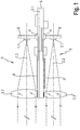
- the in Fig. 1 Laser rangefinder shown with its essential features comprises a multilayer base circuit board 3, which serves as a mechanical base, as optical and electrical shielding, as a carrier of electrical connections and as a heat conductor.
- a multilayer base circuit board 3 which serves as a mechanical base, as optical and electrical shielding, as a carrier of electrical connections and as a heat conductor.
- Essential components for this purpose are a laser transmitter 1.1, z.
- a laser diode As a laser diode, and a transmission optics 1.2, which are arranged together on one side of the base circuit board 3 and form the transmission channel 1 with a transmission axis 1.3, and a receiver 2.1, z.
- the transmission optics 1.2 and the receiving optics 2.2 are, as far as possible with mechanical aids, glued lying in a plane or in mutually parallel planes on the base circuit board 3.
- the laser transmitter 1.1 is applied to a so-called attachment circuit board 5, preferably together with a control element required for this purpose.
- the receiver 2.1 is preferably mounted on a further attachment circuit board 5 together with an amplifier stage connected thereto.
- base board and top board have been chosen to distinguish the boards. In this case, top-mounted circuit boards should be attached to the base circuit board printed circuit boards, regardless of where and via what kind of connection they are connected to the base circuit board.
- the electrical contacts are all on one end face.
- the attachment circuit boards 5 are soldered to the base board 3 on designated solder points 4 with solder.
- the attachment circuit boards 5 Prior to soldering, the attachment circuit boards 5 were adjusted to the transmission optics 1.2 and the receiving optics 2.2, so that the transmission axis 1.3 and the reception axis 2.3 are aligned parallel to each other.
- the base circuit board 3 is a multi-layer circuit board consisting of materials commonly used for this purpose.
- the copper layer 3.1 is used for optical and electrical shielding of both sides of the base circuit board 3 arranged components, as well as the heat conduction.
- the heat generated by the individual electrical and electro-optical components through the loss of heat, as well as the resulting heat by absorption in the optical components heat is mainly introduced into the base circuit board 3, where it is passed through the inner continuous copper layer 3.1 to heat sinks 6.
- the heat sinks 6 are surfaces provided with a thick copper layer, which are applied to the free areas of the surface of the base circuit board 3.
- the position of the components, and thus non-free areas, are predetermined by their function and the necessary distances from one another. However, in particular in the area of the transmitting and receiving channel 1, 2, where no further components can be arranged, there are large surfaces which, provided with the copper layer, can serve as a heat sink.
Landscapes
- Engineering & Computer Science (AREA)
- Computer Networks & Wireless Communication (AREA)
- Physics & Mathematics (AREA)
- General Physics & Mathematics (AREA)
- Radar, Positioning & Navigation (AREA)
- Remote Sensing (AREA)
- Optical Radar Systems And Details Thereof (AREA)
Claims (8)
- Dispositif de mesure d'éloignement à laser avec un canal d'émission (1), comportant un émetteur laser (1.1) et une optique d'émission (1.2) qui définissent ensemble un axe d'émission (1.3), et avec un canal de réception (2), comportant un récepteur (2.1) et une optique de réception (2.2) qui définissent ensemble un axe de réception (2.3) parallèle à l'axe d'émission (1.3), ainsi qu'une carte imprimée (3) qui est opaque pour le rayonnement de l'émetteur laser (1.1) et sur laquelle sont fixés l'émetteur laser (1.1) et le récepteur (2.1), l'émetteur laser (1.1) et l'optique d'émission (1.2) étant disposés d'un côté de la carte imprimée (3) et le récepteur (2.1) et l'optique de réception (2.2) étant disposés de l'autre côté de la carte imprimée (3),
caractérisé en ce que
la carte imprimée (3) est une carte imprimée de base (3) à plusieurs couches et à dimensions stables, qui donne au dispositif de mesure d'éloignement à laser sa stabilité mécanique et sur laquelle sont fixés tous les composants du dispositif de mesure d'éloignement à laser,
l'optique d'émission (1.2) et l'optique de réception (2.2) sont collées sur la carte imprimée de base (3), et l'émetteur laser (1.1) et le récepteur (2.1) sont chacun montés sur une carte imprimée superposée (5) respective, lesdits cartes imprimées superposées (5), ajustées respectivement par rapport à l'optique d'émission (1.2) et par rapport à l'optique de réception (2.2), étant soudées par une face sur la carte imprimée de base (3), sur des points de soudage (4) dont l'extension est supérieure à une plage de réglage nécessaire pour le réglage de l'émetteur laser (1.1) et du récepteur (2.1). - Dispositif de mesure d'éloignement à laser selon la revendication 1, caractérisé en ce que les circuits imprimés superposés (5) sont reliés aux points de soudage (4) en position verticale par rapport au circuit imprimé de base (3).
- Dispositif de mesure d'éloignement à laser selon la revendication 1, caractérisé en ce que l'émetteur laser (1.1) et le récepteur (2.1), l'optique d'émission (1.2) et l'optique de réception (2.2) et, le cas échéant, d'autres composants, sont disposés en symétrie miroir par rapport à la carte imprimée de base (3) afin de soumettre les deux côtés de la carte imprimée de base (3) à des charges mécaniques et thermiques uniformes.
- Dispositif de mesure d'éloignement à laser selon la revendication 1, caractérisé en ce que la carte imprimée de base (3) consiste en plusieurs couches non-conductrices et conductrices d'électricité, disposées en alternance, au moins une des couches conductrices d'électricité étant une couche de cuivre (3.1) continue intérieure qui sert de couche de protection optique et électrique.
- Dispositif de mesure d'éloignement à laser selon la revendication 4, caractérisé en ce que les couches non-conductrices d'électricité sont réalisées en résine époxyde renforcée avec des fibres de verre.
- Dispositif de mesure d'éloignement à laser selon la revendication 4, caractérisé en ce que les régions libres de la surface sur lesquelles aucun composé est disposé, sont revêtues d'une couche de cuivre qui sert de dissipateur thermique (6) et qui est relié à la couche de cuivre (3.1) continue intérieure.
- Dispositif de mesure d'éloignement à laser selon la revendication 1, caractérisé en ce que l'on prévoit sur la carte imprimée de base (3) des connecteurs permettant de relier le dispositif de mesure d'éloignement à laser avec un ordinateur ou une alimentation électrique.
- Dispositif de mesure d'éloignement à laser selon la revendication 1, caractérisé en ce que l'optique d'émission (1.2) et l'optique de réception (2.2) sont réalisées en polymère transparent et présentent, sur leurs circonférences, une phase planaire par laquelle l'optique d'émission (1.2) et l'optique de réception (2.2) sont chacune collées sur la carte imprimée de base (3).
Applications Claiming Priority (1)
| Application Number | Priority Date | Filing Date | Title |
|---|---|---|---|
| DE102010010097A DE102010010097A1 (de) | 2010-03-01 | 2010-03-01 | Kompakter Laser-Entfernungsmesser |
Publications (2)
| Publication Number | Publication Date |
|---|---|
| EP2363726A1 EP2363726A1 (fr) | 2011-09-07 |
| EP2363726B1 true EP2363726B1 (fr) | 2017-09-20 |
Family
ID=43929095
Family Applications (1)
| Application Number | Title | Priority Date | Filing Date |
|---|---|---|---|
| EP11156147.8A Active EP2363726B1 (fr) | 2010-03-01 | 2011-02-28 | Dispositif de mesure d'éloignement à laser compact |
Country Status (4)
| Country | Link |
|---|---|
| US (1) | US8842260B2 (fr) |
| EP (1) | EP2363726B1 (fr) |
| DE (1) | DE102010010097A1 (fr) |
| DK (1) | DK2363726T3 (fr) |
Families Citing this family (21)
| Publication number | Priority date | Publication date | Assignee | Title |
|---|---|---|---|---|
| USRE46672E1 (en) | 2006-07-13 | 2018-01-16 | Velodyne Lidar, Inc. | High definition LiDAR system |
| WO2013113456A1 (fr) * | 2012-02-03 | 2013-08-08 | Mechaless Systems Gmbh | Compensation d'un capteur optique par le biais du circuit imprimé |
| JP6220672B2 (ja) * | 2013-12-27 | 2017-10-25 | パナソニック デバイスSunx株式会社 | 変位センサ |
| US9563035B2 (en) * | 2014-04-03 | 2017-02-07 | Ikegps Group Limited | Mirror mounting assembly for mounting a mirror in a laser rangefinder |
| DE102014116121B3 (de) * | 2014-11-05 | 2015-10-22 | Esw Gmbh | Kompakter Laser-Entfernungsmesser mit erhöhter Reichweite |
| US10627490B2 (en) | 2016-01-31 | 2020-04-21 | Velodyne Lidar, Inc. | Multiple pulse, LIDAR based 3-D imaging |
| US10018726B2 (en) | 2016-03-19 | 2018-07-10 | Velodyne Lidar, Inc. | Integrated illumination and detection for LIDAR based 3-D imaging |
| WO2017210418A1 (fr) | 2016-06-01 | 2017-12-07 | Velodyne Lidar, Inc. | Lidar à balayage à pixels multiples |
| DE102016112557B4 (de) | 2016-07-08 | 2019-08-22 | Jenoptik Advanced Systems Gmbh | Optische Stahlformungseinheit und Entfernungsmessvorrichtung |
| WO2018183843A1 (fr) | 2017-03-31 | 2018-10-04 | Velodyne Lidar, Inc. | Commande de puissance d'éclairage à lidar intégré |
| EP3612798A4 (fr) | 2017-05-08 | 2021-01-13 | Velodyne Lidar, Inc. | Acquisition et commande de données lidar |
| US11294041B2 (en) | 2017-12-08 | 2022-04-05 | Velodyne Lidar Usa, Inc. | Systems and methods for improving detection of a return signal in a light ranging and detection system |
| CN108226946A (zh) * | 2018-01-23 | 2018-06-29 | 中国航空工业集团公司洛阳电光设备研究所 | 激光测距机及其信号单元底座 |
| US11971507B2 (en) | 2018-08-24 | 2024-04-30 | Velodyne Lidar Usa, Inc. | Systems and methods for mitigating optical crosstalk in a light ranging and detection system |
| US10712434B2 (en) | 2018-09-18 | 2020-07-14 | Velodyne Lidar, Inc. | Multi-channel LIDAR illumination driver |
| US11082010B2 (en) | 2018-11-06 | 2021-08-03 | Velodyne Lidar Usa, Inc. | Systems and methods for TIA base current detection and compensation |
| US11885958B2 (en) | 2019-01-07 | 2024-01-30 | Velodyne Lidar Usa, Inc. | Systems and methods for a dual axis resonant scanning mirror |
| US10613203B1 (en) | 2019-07-01 | 2020-04-07 | Velodyne Lidar, Inc. | Interference mitigation for light detection and ranging |
| FR3102886A1 (fr) | 2019-10-30 | 2021-05-07 | Stmicroelectronics (Grenoble 2) Sas | Dispositif optoélectronique |
| FR3102863B1 (fr) | 2019-10-31 | 2021-11-12 | St Microelectronics Grenoble 2 | Dispositif optoélectronique |
| US11005519B1 (en) * | 2020-05-01 | 2021-05-11 | UTVATE Corporation | Isolation methods for full-duplex antenna systems |
Family Cites Families (27)
| Publication number | Priority date | Publication date | Assignee | Title |
|---|---|---|---|---|
| US3697762A (en) * | 1970-12-14 | 1972-10-10 | Philips Corp | Photo electric switching device |
| JPH0726842B2 (ja) * | 1987-02-06 | 1995-03-29 | 松下電工株式会社 | 光センサ |
| ATE223120T1 (de) * | 1994-12-22 | 2002-09-15 | Optosys Ag | Näherungsschalter |
| JPH09127406A (ja) | 1995-10-31 | 1997-05-16 | Olympus Optical Co Ltd | 測距装置 |
| DE19718157A1 (de) * | 1997-04-29 | 1998-11-05 | Sick Ag | Opto-elektronischer Sensor |
| JP3105832B2 (ja) | 1997-06-30 | 2000-11-06 | 静岡日本電気株式会社 | 携帯型パーソナルコンピュータ |
| US6160250A (en) * | 1999-03-31 | 2000-12-12 | Hewlett-Packard Company | Integrated optical imaging assembly |
| ATE301276T1 (de) * | 2000-12-11 | 2005-08-15 | Mitsubishi Electric Corp | Optischer distanzsensor |
| DE10062108B4 (de) * | 2000-12-13 | 2010-04-15 | Infineon Technologies Ag | Leistungsmodul mit verbessertem transienten Wärmewiderstand |
| DE20221470U1 (de) * | 2001-01-19 | 2006-03-16 | Leuze Electronic Gmbh + Co. Kg | Optoelektronische Vorrichtung |
| CN1248209C (zh) * | 2001-04-05 | 2006-03-29 | 皇家菲利浦电子有限公司 | 光学扫描装置 |
| DE10157378B4 (de) * | 2001-11-22 | 2012-10-25 | Robert Bosch Gmbh | Messgerät zur berührungslosen Abstandsmessung |
| DE10221074B4 (de) * | 2002-05-10 | 2004-08-05 | Dihag Deutsche Giesserei- Und Industrie-Holding Ag | Gießform zur Herstellung eines Gußteils unter Verwendung von Formgrundstoff und Verwendung einer solchen Gießform |
| DE10323857A1 (de) * | 2003-05-26 | 2005-01-27 | Osram Opto Semiconductors Gmbh | Gehäuse für ein Laserdiodenbauelement, Laserdiodenbauelement und Verfahren zum Herstellen eines Laserdiodenbauelements |
| DE10331074A1 (de) | 2003-07-09 | 2005-02-03 | Conti Temic Microelectronic Gmbh | Sensoranordnung zur Abstands- und/oder Geschwindigkeitsmessung |
| DE102004018476B4 (de) * | 2004-04-16 | 2009-06-18 | Infineon Technologies Ag | Leistungshalbleiteranordnung mit kontaktierender Folie und Anpressvorrichtung |
| US7036999B2 (en) * | 2004-05-14 | 2006-05-02 | Schroedinger Karl | Optoelectronic module and optoelectronic system |
| US7217043B2 (en) * | 2004-10-06 | 2007-05-15 | Infineon Technologies Fiber Optics Gmbh | Optoelectronic transceiver |
| US7703201B2 (en) * | 2004-10-25 | 2010-04-27 | International Business Machines Corporation | Method of embedding tamper proof layers and discrete components into printed circuit board stack-up |
| US7235745B2 (en) * | 2005-01-10 | 2007-06-26 | Endicott Interconnect Technologies, Inc. | Resistor material with metal component for use in circuitized substrates, circuitized substrate utilizing same, method of making said ciruitized substrate, and information handling system utilizing said ciruitized substrate |
| DE102005035417A1 (de) * | 2005-07-28 | 2007-02-01 | Robert Bosch Gmbh | Entfernungsmessgerät und Verfahren zum Befestigen einer elektrooptischen Einheit an einer Leiterträgereinheit |
| JP4819431B2 (ja) * | 2005-07-29 | 2011-11-24 | 株式会社日本ディックス | ハンダレス接続用のコネクタとこのコネクタに接続されるプラグ |
| DE102005041998B4 (de) | 2005-09-05 | 2018-11-29 | Robert Bosch Gmbh | Verfahren zur Justage eines abbildenden Elements sowie Messgerät justiert nach einem derartigen Verfahren |
| DE102006028675B4 (de) * | 2006-06-22 | 2008-08-21 | Siemens Ag | Kühlanordnung für auf einer Trägerplatte angeordnete elektrische Bauelemente |
| DE102007007380B4 (de) * | 2007-02-12 | 2011-02-03 | Carl Zeiss Sports Optics Gmbh | Binokulares Fernglas |
| US8323436B2 (en) * | 2007-03-28 | 2012-12-04 | The United States Of America As Represented By The Secretary Of The Army | Transparent, reinforced, composite fiber and articles made therefrom |
| EP2116867A3 (fr) * | 2008-04-15 | 2010-03-03 | Pepperl + Fuchs Gmbh | Capteur optique |
-
2010
- 2010-03-01 DE DE102010010097A patent/DE102010010097A1/de not_active Ceased
-
2011
- 2011-02-28 EP EP11156147.8A patent/EP2363726B1/fr active Active
- 2011-02-28 DK DK11156147.8T patent/DK2363726T3/en active
- 2011-03-01 US US13/037,702 patent/US8842260B2/en active Active
Non-Patent Citations (1)
| Title |
|---|
| None * |
Also Published As
| Publication number | Publication date |
|---|---|
| US8842260B2 (en) | 2014-09-23 |
| EP2363726A1 (fr) | 2011-09-07 |
| DK2363726T3 (en) | 2018-01-08 |
| US20110211188A1 (en) | 2011-09-01 |
| DE102010010097A1 (de) | 2011-09-01 |
Similar Documents
| Publication | Publication Date | Title |
|---|---|---|
| EP2363726B1 (fr) | Dispositif de mesure d'éloignement à laser compact | |
| EP2527866B1 (fr) | Dispositif de mesure de la distance | |
| EP1913416B1 (fr) | Télémètre électro-optique | |
| EP2073047B1 (fr) | Procédé de montage et d'ajustage d'un dispositif électro-optique et dispositif de mesure monté et ajusté selon un tel procédé | |
| DE102005041980B4 (de) | Elektro-optisches Messgerät | |
| EP0155528A1 (fr) | Logement à module optoélectronique | |
| EP2411834B1 (fr) | Support d'optique céramique | |
| EP2527867A1 (fr) | Dispositif de mesure de la distance | |
| DE112014001559T5 (de) | Bildsensor | |
| DE102014116121B3 (de) | Kompakter Laser-Entfernungsmesser mit erhöhter Reichweite | |
| EP1913415B1 (fr) | Appareil de telemetrie et procede pour fixer une unite electro-optique a une unite support de conducteurs | |
| DE102017203489A1 (de) | Kameravorrichtung | |
| DE102005041998B4 (de) | Verfahren zur Justage eines abbildenden Elements sowie Messgerät justiert nach einem derartigen Verfahren | |
| DE10344767B4 (de) | Optisches Modul und optisches System | |
| DE102014110510A1 (de) | Leiterplatinensatz für die Sende- und Empfangskombination einer optoelektronischen Detektionseinrichtung, Detektionseinrichtung mit einem solchen Leiterplattensatz sowie Kraftfahrzeug mit einer solchen Detektionseinrichtung | |
| EP2930063A2 (fr) | Unité de clignotant pour un dispositif de vue indirecte d'un véhicule et dispositif de vue indirecte doté d'une unité de clignotant | |
| EP1141662B1 (fr) | Module de mesure tridimensionnel | |
| EP3355075B1 (fr) | Système de détection | |
| DE102016121913A1 (de) | Mehrstrahllichtschranke | |
| EP1999869A1 (fr) | Systeme de bus de donnees | |
| EP3159712A1 (fr) | Procédé de liaison d'un groupe d'émission et d'un groupe de réception à une combinaison d'émission et de réception d'un dispositif de détection optoélectronique et dispositif de détection et véhicule en étant équipé | |
| EP0172485B1 (fr) | Boîtier commun pour deux corps semi-conducteurs | |
| DE202016106394U1 (de) | Mehrstrahllichtschranke | |
| EP2192420A1 (fr) | Unité d'émission et de réception optique et capteur doté de celle-ci | |
| WO2017042096A1 (fr) | Unité d'émission et/ou de réception d'un dispositif de mesure optique et dispositif de mesure optique |
Legal Events
| Date | Code | Title | Description |
|---|---|---|---|
| PUAI | Public reference made under article 153(3) epc to a published international application that has entered the european phase |
Free format text: ORIGINAL CODE: 0009012 |
|
| AK | Designated contracting states |
Kind code of ref document: A1 Designated state(s): AL AT BE BG CH CY CZ DE DK EE ES FI FR GB GR HR HU IE IS IT LI LT LU LV MC MK MT NL NO PL PT RO RS SE SI SK SM TR |
|
| AX | Request for extension of the european patent |
Extension state: BA ME |
|
| 17P | Request for examination filed |
Effective date: 20120224 |
|
| 17Q | First examination report despatched |
Effective date: 20151028 |
|
| RAP1 | Party data changed (applicant data changed or rights of an application transferred) |
Owner name: JENOPTIK ADVANCED SYSTEMS GMBH |
|
| GRAP | Despatch of communication of intention to grant a patent |
Free format text: ORIGINAL CODE: EPIDOSNIGR1 |
|
| INTG | Intention to grant announced |
Effective date: 20170412 |
|
| GRAS | Grant fee paid |
Free format text: ORIGINAL CODE: EPIDOSNIGR3 |
|
| GRAA | (expected) grant |
Free format text: ORIGINAL CODE: 0009210 |
|
| AK | Designated contracting states |
Kind code of ref document: B1 Designated state(s): AL AT BE BG CH CY CZ DE DK EE ES FI FR GB GR HR HU IE IS IT LI LT LU LV MC MK MT NL NO PL PT RO RS SE SI SK SM TR |
|
| REG | Reference to a national code |
Ref country code: GB Ref legal event code: FG4D Free format text: NOT ENGLISH |
|
| REG | Reference to a national code |
Ref country code: CH Ref legal event code: EP |
|
| REG | Reference to a national code |
Ref country code: AT Ref legal event code: REF Ref document number: 930587 Country of ref document: AT Kind code of ref document: T Effective date: 20171015 |
|
| REG | Reference to a national code |
Ref country code: IE Ref legal event code: FG4D Free format text: LANGUAGE OF EP DOCUMENT: GERMAN |
|
| REG | Reference to a national code |
Ref country code: DE Ref legal event code: R096 Ref document number: 502011013011 Country of ref document: DE |
|
| REG | Reference to a national code |
Ref country code: DK Ref legal event code: T3 Effective date: 20180105 |
|
| REG | Reference to a national code |
Ref country code: NL Ref legal event code: MP Effective date: 20170920 |
|
| PG25 | Lapsed in a contracting state [announced via postgrant information from national office to epo] |
Ref country code: HR Free format text: LAPSE BECAUSE OF FAILURE TO SUBMIT A TRANSLATION OF THE DESCRIPTION OR TO PAY THE FEE WITHIN THE PRESCRIBED TIME-LIMIT Effective date: 20170920 Ref country code: NO Free format text: LAPSE BECAUSE OF FAILURE TO SUBMIT A TRANSLATION OF THE DESCRIPTION OR TO PAY THE FEE WITHIN THE PRESCRIBED TIME-LIMIT Effective date: 20171220 Ref country code: SE Free format text: LAPSE BECAUSE OF FAILURE TO SUBMIT A TRANSLATION OF THE DESCRIPTION OR TO PAY THE FEE WITHIN THE PRESCRIBED TIME-LIMIT Effective date: 20170920 Ref country code: LT Free format text: LAPSE BECAUSE OF FAILURE TO SUBMIT A TRANSLATION OF THE DESCRIPTION OR TO PAY THE FEE WITHIN THE PRESCRIBED TIME-LIMIT Effective date: 20170920 |
|
| REG | Reference to a national code |
Ref country code: LT Ref legal event code: MG4D |
|
| REG | Reference to a national code |
Ref country code: FR Ref legal event code: PLFP Year of fee payment: 8 |
|
| PG25 | Lapsed in a contracting state [announced via postgrant information from national office to epo] |
Ref country code: GR Free format text: LAPSE BECAUSE OF FAILURE TO SUBMIT A TRANSLATION OF THE DESCRIPTION OR TO PAY THE FEE WITHIN THE PRESCRIBED TIME-LIMIT Effective date: 20171221 Ref country code: RS Free format text: LAPSE BECAUSE OF FAILURE TO SUBMIT A TRANSLATION OF THE DESCRIPTION OR TO PAY THE FEE WITHIN THE PRESCRIBED TIME-LIMIT Effective date: 20170920 Ref country code: LV Free format text: LAPSE BECAUSE OF FAILURE TO SUBMIT A TRANSLATION OF THE DESCRIPTION OR TO PAY THE FEE WITHIN THE PRESCRIBED TIME-LIMIT Effective date: 20170920 Ref country code: BG Free format text: LAPSE BECAUSE OF FAILURE TO SUBMIT A TRANSLATION OF THE DESCRIPTION OR TO PAY THE FEE WITHIN THE PRESCRIBED TIME-LIMIT Effective date: 20171220 |
|
| PG25 | Lapsed in a contracting state [announced via postgrant information from national office to epo] |
Ref country code: NL Free format text: LAPSE BECAUSE OF FAILURE TO SUBMIT A TRANSLATION OF THE DESCRIPTION OR TO PAY THE FEE WITHIN THE PRESCRIBED TIME-LIMIT Effective date: 20170920 |
|
| PG25 | Lapsed in a contracting state [announced via postgrant information from national office to epo] |
Ref country code: RO Free format text: LAPSE BECAUSE OF FAILURE TO SUBMIT A TRANSLATION OF THE DESCRIPTION OR TO PAY THE FEE WITHIN THE PRESCRIBED TIME-LIMIT Effective date: 20170920 Ref country code: ES Free format text: LAPSE BECAUSE OF FAILURE TO SUBMIT A TRANSLATION OF THE DESCRIPTION OR TO PAY THE FEE WITHIN THE PRESCRIBED TIME-LIMIT Effective date: 20170920 Ref country code: CZ Free format text: LAPSE BECAUSE OF FAILURE TO SUBMIT A TRANSLATION OF THE DESCRIPTION OR TO PAY THE FEE WITHIN THE PRESCRIBED TIME-LIMIT Effective date: 20170920 Ref country code: PL Free format text: LAPSE BECAUSE OF FAILURE TO SUBMIT A TRANSLATION OF THE DESCRIPTION OR TO PAY THE FEE WITHIN THE PRESCRIBED TIME-LIMIT Effective date: 20170920 |
|
| PG25 | Lapsed in a contracting state [announced via postgrant information from national office to epo] |
Ref country code: EE Free format text: LAPSE BECAUSE OF FAILURE TO SUBMIT A TRANSLATION OF THE DESCRIPTION OR TO PAY THE FEE WITHIN THE PRESCRIBED TIME-LIMIT Effective date: 20170920 Ref country code: IS Free format text: LAPSE BECAUSE OF FAILURE TO SUBMIT A TRANSLATION OF THE DESCRIPTION OR TO PAY THE FEE WITHIN THE PRESCRIBED TIME-LIMIT Effective date: 20180120 Ref country code: SM Free format text: LAPSE BECAUSE OF FAILURE TO SUBMIT A TRANSLATION OF THE DESCRIPTION OR TO PAY THE FEE WITHIN THE PRESCRIBED TIME-LIMIT Effective date: 20170920 Ref country code: SK Free format text: LAPSE BECAUSE OF FAILURE TO SUBMIT A TRANSLATION OF THE DESCRIPTION OR TO PAY THE FEE WITHIN THE PRESCRIBED TIME-LIMIT Effective date: 20170920 |
|
| REG | Reference to a national code |
Ref country code: DE Ref legal event code: R097 Ref document number: 502011013011 Country of ref document: DE |
|
| PLBE | No opposition filed within time limit |
Free format text: ORIGINAL CODE: 0009261 |
|
| STAA | Information on the status of an ep patent application or granted ep patent |
Free format text: STATUS: NO OPPOSITION FILED WITHIN TIME LIMIT |
|
| 26N | No opposition filed |
Effective date: 20180621 |
|
| REG | Reference to a national code |
Ref country code: CH Ref legal event code: PL |
|
| PG25 | Lapsed in a contracting state [announced via postgrant information from national office to epo] |
Ref country code: MT Free format text: LAPSE BECAUSE OF FAILURE TO SUBMIT A TRANSLATION OF THE DESCRIPTION OR TO PAY THE FEE WITHIN THE PRESCRIBED TIME-LIMIT Effective date: 20170920 Ref country code: MC Free format text: LAPSE BECAUSE OF FAILURE TO SUBMIT A TRANSLATION OF THE DESCRIPTION OR TO PAY THE FEE WITHIN THE PRESCRIBED TIME-LIMIT Effective date: 20170920 |
|
| REG | Reference to a national code |
Ref country code: IE Ref legal event code: MM4A |
|
| REG | Reference to a national code |
Ref country code: BE Ref legal event code: MM Effective date: 20180228 |
|
| PG25 | Lapsed in a contracting state [announced via postgrant information from national office to epo] |
Ref country code: CH Free format text: LAPSE BECAUSE OF NON-PAYMENT OF DUE FEES Effective date: 20180228 Ref country code: LI Free format text: LAPSE BECAUSE OF NON-PAYMENT OF DUE FEES Effective date: 20180228 Ref country code: SI Free format text: LAPSE BECAUSE OF FAILURE TO SUBMIT A TRANSLATION OF THE DESCRIPTION OR TO PAY THE FEE WITHIN THE PRESCRIBED TIME-LIMIT Effective date: 20170920 Ref country code: LU Free format text: LAPSE BECAUSE OF NON-PAYMENT OF DUE FEES Effective date: 20180228 |
|
| PG25 | Lapsed in a contracting state [announced via postgrant information from national office to epo] |
Ref country code: IE Free format text: LAPSE BECAUSE OF NON-PAYMENT OF DUE FEES Effective date: 20180228 |
|
| PG25 | Lapsed in a contracting state [announced via postgrant information from national office to epo] |
Ref country code: BE Free format text: LAPSE BECAUSE OF NON-PAYMENT OF DUE FEES Effective date: 20180228 |
|
| REG | Reference to a national code |
Ref country code: DE Ref legal event code: R082 Ref document number: 502011013011 Country of ref document: DE Representative=s name: WALDAUF, ALEXANDER, DIPL.-ING. DR.-ING., DE Ref country code: DE Ref legal event code: R081 Ref document number: 502011013011 Country of ref document: DE Owner name: JENOPTIK OPTICAL SYSTEMS GMBH, DE Free format text: FORMER OWNER: JENOPTIK ADVANCED SYSTEMS GMBH, 22880 WEDEL, DE |
|
| PG25 | Lapsed in a contracting state [announced via postgrant information from national office to epo] |
Ref country code: TR Free format text: LAPSE BECAUSE OF FAILURE TO SUBMIT A TRANSLATION OF THE DESCRIPTION OR TO PAY THE FEE WITHIN THE PRESCRIBED TIME-LIMIT Effective date: 20170920 |
|
| REG | Reference to a national code |
Ref country code: GB Ref legal event code: 732E Free format text: REGISTERED BETWEEN 20200305 AND 20200311 |
|
| REG | Reference to a national code |
Ref country code: FI Ref legal event code: PCE Owner name: JENOPTIK OPTICAL SYSTEMS GMBH |
|
| PG25 | Lapsed in a contracting state [announced via postgrant information from national office to epo] |
Ref country code: HU Free format text: LAPSE BECAUSE OF FAILURE TO SUBMIT A TRANSLATION OF THE DESCRIPTION OR TO PAY THE FEE WITHIN THE PRESCRIBED TIME-LIMIT; INVALID AB INITIO Effective date: 20110228 Ref country code: PT Free format text: LAPSE BECAUSE OF FAILURE TO SUBMIT A TRANSLATION OF THE DESCRIPTION OR TO PAY THE FEE WITHIN THE PRESCRIBED TIME-LIMIT Effective date: 20170920 |
|
| REG | Reference to a national code |
Ref country code: BE Ref legal event code: PD Owner name: JENOPTIK OPTICAL SYSTEMS GMBH; DE Free format text: DETAILS ASSIGNMENT: CHANGE OF OWNER(S), FUSION; FORMER OWNER NAME: JENOPTIK ADVANCED SYSTEMS GMBH Effective date: 20200217 Ref country code: BE Ref legal event code: PD Owner name: JENOPTIK ADVANCED SYSTEMS GMBH; DE Free format text: DETAILS ASSIGNMENT: CHANGE OF OWNER(S), FUSION; FORMER OWNER NAME: JENOPTIK OPTICAL SYSTEMS GMBH Effective date: 20200217 |
|
| PG25 | Lapsed in a contracting state [announced via postgrant information from national office to epo] |
Ref country code: MK Free format text: LAPSE BECAUSE OF NON-PAYMENT OF DUE FEES Effective date: 20170920 Ref country code: CY Free format text: LAPSE BECAUSE OF FAILURE TO SUBMIT A TRANSLATION OF THE DESCRIPTION OR TO PAY THE FEE WITHIN THE PRESCRIBED TIME-LIMIT Effective date: 20170920 |
|
| PG25 | Lapsed in a contracting state [announced via postgrant information from national office to epo] |
Ref country code: AL Free format text: LAPSE BECAUSE OF FAILURE TO SUBMIT A TRANSLATION OF THE DESCRIPTION OR TO PAY THE FEE WITHIN THE PRESCRIBED TIME-LIMIT Effective date: 20170920 |
|
| REG | Reference to a national code |
Ref country code: AT Ref legal event code: PC Ref document number: 930587 Country of ref document: AT Kind code of ref document: T Owner name: JENOPTIK OPTICAL SYSTEMS GMBH, DE Effective date: 20200625 |
|
| PGFP | Annual fee paid to national office [announced via postgrant information from national office to epo] |
Ref country code: FI Payment date: 20210216 Year of fee payment: 11 |
|
| PGFP | Annual fee paid to national office [announced via postgrant information from national office to epo] |
Ref country code: GB Payment date: 20210222 Year of fee payment: 11 Ref country code: AT Payment date: 20210216 Year of fee payment: 11 |
|
| REG | Reference to a national code |
Ref country code: FI Ref legal event code: MAE |
|
| REG | Reference to a national code |
Ref country code: AT Ref legal event code: MM01 Ref document number: 930587 Country of ref document: AT Kind code of ref document: T Effective date: 20220228 |
|
| GBPC | Gb: european patent ceased through non-payment of renewal fee |
Effective date: 20220228 |
|
| PG25 | Lapsed in a contracting state [announced via postgrant information from national office to epo] |
Ref country code: FI Free format text: LAPSE BECAUSE OF NON-PAYMENT OF DUE FEES Effective date: 20220228 Ref country code: AT Free format text: LAPSE BECAUSE OF NON-PAYMENT OF DUE FEES Effective date: 20220228 |
|
| PG25 | Lapsed in a contracting state [announced via postgrant information from national office to epo] |
Ref country code: GB Free format text: LAPSE BECAUSE OF NON-PAYMENT OF DUE FEES Effective date: 20220228 |
|
| PGFP | Annual fee paid to national office [announced via postgrant information from national office to epo] |
Ref country code: FR Payment date: 20230217 Year of fee payment: 13 Ref country code: DK Payment date: 20230220 Year of fee payment: 13 |
|
| PGFP | Annual fee paid to national office [announced via postgrant information from national office to epo] |
Ref country code: IT Payment date: 20230228 Year of fee payment: 13 |
|
| PGFP | Annual fee paid to national office [announced via postgrant information from national office to epo] |
Ref country code: DE Payment date: 20240216 Year of fee payment: 14 |