EP2362409A2 - Light emitting substrate, manufacturing method thereof, and image display apparatus having the light emitting substrate - Google Patents
Light emitting substrate, manufacturing method thereof, and image display apparatus having the light emitting substrate Download PDFInfo
- Publication number
- EP2362409A2 EP2362409A2 EP11153202A EP11153202A EP2362409A2 EP 2362409 A2 EP2362409 A2 EP 2362409A2 EP 11153202 A EP11153202 A EP 11153202A EP 11153202 A EP11153202 A EP 11153202A EP 2362409 A2 EP2362409 A2 EP 2362409A2
- Authority
- EP
- European Patent Office
- Prior art keywords
- light emitting
- substrate
- rib
- light
- shielding layer
- Prior art date
- Legal status (The legal status is an assumption and is not a legal conclusion. Google has not performed a legal analysis and makes no representation as to the accuracy of the status listed.)
- Withdrawn
Links
- 239000000758 substrate Substances 0.000 title claims abstract description 87
- 238000004519 manufacturing process Methods 0.000 title claims description 13
- 238000000034 method Methods 0.000 description 15
- 230000015572 biosynthetic process Effects 0.000 description 11
- 239000004615 ingredient Substances 0.000 description 11
- 239000010408 film Substances 0.000 description 10
- 238000005192 partition Methods 0.000 description 10
- 239000000463 material Substances 0.000 description 9
- 229910052751 metal Inorganic materials 0.000 description 9
- 239000002184 metal Substances 0.000 description 9
- 238000000206 photolithography Methods 0.000 description 7
- 238000007650 screen-printing Methods 0.000 description 7
- 229920005989 resin Polymers 0.000 description 6
- 239000011347 resin Substances 0.000 description 6
- 239000011521 glass Substances 0.000 description 5
- 239000011159 matrix material Substances 0.000 description 5
- 239000002904 solvent Substances 0.000 description 5
- 230000000694 effects Effects 0.000 description 4
- 125000006850 spacer group Chemical group 0.000 description 4
- 239000003505 polymerization initiator Substances 0.000 description 3
- 238000012545 processing Methods 0.000 description 3
- 239000010409 thin film Substances 0.000 description 3
- 238000007740 vapor deposition Methods 0.000 description 3
- XEEYBQQBJWHFJM-UHFFFAOYSA-N Iron Chemical compound [Fe] XEEYBQQBJWHFJM-UHFFFAOYSA-N 0.000 description 2
- 229910052782 aluminium Inorganic materials 0.000 description 2
- XAGFODPZIPBFFR-UHFFFAOYSA-N aluminium Chemical compound [Al] XAGFODPZIPBFFR-UHFFFAOYSA-N 0.000 description 2
- 239000002772 conduction electron Substances 0.000 description 2
- 238000011161 development Methods 0.000 description 2
- 238000012986 modification Methods 0.000 description 2
- 230000004048 modification Effects 0.000 description 2
- 239000002245 particle Substances 0.000 description 2
- 239000011295 pitch Substances 0.000 description 2
- 238000004544 sputter deposition Methods 0.000 description 2
- 238000004804 winding Methods 0.000 description 2
- PWHULOQIROXLJO-UHFFFAOYSA-N Manganese Chemical compound [Mn] PWHULOQIROXLJO-UHFFFAOYSA-N 0.000 description 1
- RTAQQCXQSZGOHL-UHFFFAOYSA-N Titanium Chemical compound [Ti] RTAQQCXQSZGOHL-UHFFFAOYSA-N 0.000 description 1
- 238000013459 approach Methods 0.000 description 1
- 239000010941 cobalt Substances 0.000 description 1
- 229910017052 cobalt Inorganic materials 0.000 description 1
- GUTLYIVDDKVIGB-UHFFFAOYSA-N cobalt atom Chemical compound [Co] GUTLYIVDDKVIGB-UHFFFAOYSA-N 0.000 description 1
- 239000002131 composite material Substances 0.000 description 1
- 230000007423 decrease Effects 0.000 description 1
- 230000002542 deteriorative effect Effects 0.000 description 1
- 238000005516 engineering process Methods 0.000 description 1
- 238000005530 etching Methods 0.000 description 1
- 238000010304 firing Methods 0.000 description 1
- 239000001023 inorganic pigment Substances 0.000 description 1
- 229910052742 iron Inorganic materials 0.000 description 1
- 229910052748 manganese Inorganic materials 0.000 description 1
- 239000011572 manganese Substances 0.000 description 1
- 229910044991 metal oxide Inorganic materials 0.000 description 1
- 229920003986 novolac Polymers 0.000 description 1
- 238000000059 patterning Methods 0.000 description 1
- 239000010936 titanium Substances 0.000 description 1
- 229910052719 titanium Inorganic materials 0.000 description 1
- XLYOFNOQVPJJNP-UHFFFAOYSA-N water Substances O XLYOFNOQVPJJNP-UHFFFAOYSA-N 0.000 description 1
Images

Classifications
-
- H—ELECTRICITY
- H01—ELECTRIC ELEMENTS
- H01J—ELECTRIC DISCHARGE TUBES OR DISCHARGE LAMPS
- H01J31/00—Cathode ray tubes; Electron beam tubes
- H01J31/08—Cathode ray tubes; Electron beam tubes having a screen on or from which an image or pattern is formed, picked up, converted, or stored
- H01J31/10—Image or pattern display tubes, i.e. having electrical input and optical output; Flying-spot tubes for scanning purposes
- H01J31/12—Image or pattern display tubes, i.e. having electrical input and optical output; Flying-spot tubes for scanning purposes with luminescent screen
- H01J31/123—Flat display tubes
- H01J31/125—Flat display tubes provided with control means permitting the electron beam to reach selected parts of the screen, e.g. digital selection
- H01J31/127—Flat display tubes provided with control means permitting the electron beam to reach selected parts of the screen, e.g. digital selection using large area or array sources, i.e. essentially a source for each pixel group
-
- H—ELECTRICITY
- H01—ELECTRIC ELEMENTS
- H01J—ELECTRIC DISCHARGE TUBES OR DISCHARGE LAMPS
- H01J29/00—Details of cathode-ray tubes or of electron-beam tubes of the types covered by group H01J31/00
- H01J29/86—Vessels; Containers; Vacuum locks
- H01J29/864—Spacers between faceplate and backplate of flat panel cathode ray tubes
-
- H—ELECTRICITY
- H01—ELECTRIC ELEMENTS
- H01J—ELECTRIC DISCHARGE TUBES OR DISCHARGE LAMPS
- H01J9/00—Apparatus or processes specially adapted for the manufacture, installation, removal, maintenance of electric discharge tubes, discharge lamps, or parts thereof; Recovery of material from discharge tubes or lamps
- H01J9/24—Manufacture or joining of vessels, leading-in conductors or bases
- H01J9/241—Manufacture or joining of vessels, leading-in conductors or bases the vessel being for a flat panel display
- H01J9/242—Spacers between faceplate and backplate
Definitions
- the present invention relates to a light emitting substrate having a light emitting layer which emits light in response to electrons bombarded thereon, a manufacturing method of the light emitting substrate, and an image display apparatus provided with the light emitting substrate which is used in, for example, a television.
- Flat panel displays also referred to as flatscreen displays
- PDP plasma display
- FED field emission display
- Some of these display apparatuses may adopt a rib (partition wall) structure to partition a discharge cell.
- ribs are desirably formed to be heightened to increase a surface area of a fluorescent member contributing to discharge-induced light emission.
- ribs desirably have a small width to optimize the density of display pixels. As a consequence, it is necessary that the ribs be formed in such a shape that an aspect ratio is high.
- Japanese Patent Application Laid-Open No. 2004-111302 discusses an image display apparatus where a rib structure having a winding shape with bent sections is provided to prevent any external force from acting on the ribs, causing them to collapse.
- Japanese Patent Application Laid-Open No. 2001-23515 discusses an image display apparatus wherein auxiliary ribs are additionally formed in a rib structure to increase a total area where the ribs are joined so that increased structural strength is obtained.
- 2001-118512 discusses an image display apparatus provided with bilayered partition walls having a lower partition wall section formed on a substrate surface and an upper partition wall section formed on the lower partition wall section, wherein the whole of the lower partition wall sections of the lengthwise partition walls in parallel with address electrodes and the crosswise partition walls in parallel with bus electrodes constitutes the lower partition wall sections.
- the present invention is directed to a rib structure having a remarkable strength that can prevent ribs from collapsing in a finely-pitched pixel layout, in an image display apparatus provided with a light emitting substrate having a light emitting layer which emits light in response to electrons bombarded thereon, and to an image display apparatus having a distinguished display property which accomplishes a high definition in image display.
- the present invention in its first aspect provides a light emitting substrate as specified in claim 1.
- the present invention in its second aspect provides an image display apparatus as specified in claim 2.
- the present invention in its third aspect provides a manufacturing method of a light emitting substrate as specified in claims 3 and 4.
- the wall rib and the sheet rib are combined to constitute the rib structure, the risk of collapse of the ribs can be eliminated even in a densely-pitched pixel layout.
- the light shielding layer is used as a mask to expose the substrate to light from the rear surface thereof so that the sheet rib can be self-aligned to the openings of the light shielding layer, which further improves the definition in image display.
- the wall surface of the sheet rib is formed tilting toward the openings of the light shielding layer.
- the light emitting layer is formed, therefore, the effect of self alignment facilitates the formation of the light emitting layer having an equal film thickness.
- the present invention can provide an image display apparatus having a distinguished display property which achieves a high definition in image display.
- Fig. 1 schematically illustrates cross sections showing steps of forming a rib structure of a light emitting substrate according to the present invention.
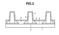
- Fig. 2 schematically illustrates a cross section showing an example of the light emitting substrate according to the present invention.
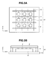
- Figs. 3A and 3B schematically illustrate an image display apparatus according to the present invention and an electron source substrate used in the image display apparatus.
- Fig. 1 schematically illustrates a cross section as an example of the light emitting substrate according to the present invention.
- the emitting substrate includes a substrate 1, a light shielding layer 2, an opening 3 formed in the light shielding layer 2, a wall rib 4, a sheet rib 5, a light emitting layer 6, and a metal back layer 7 as illustrated in Fig. 2 .
- Fig. 1 schematically illustrates cross sections in processing for forming the light emitting substrate illustrated in Fig. 2 .
- Fig. 1 schematically illustrates cross sections in processing for forming the light emitting substrate illustrated in Fig. 2 .
- FIG. 2 is a cross-sectional schematic illustration of (a-3) , (b-3) , and (c-3) illustrated in Fig. 1 .
- the light shielding layer 2 having a plurality of openings 3 is formed on a surface (main surface) of the substrate 1.
- a member which transmits a visible light therethrough such as a glass substrate, is used as the substrate 1.
- a glass with a high strain point for example, "PD200" supplied by ASAHI GLASS CO. , LTD is suitably used.
- the light shielding layer 2 is a black matrix in which openings 3 are provided in the form of dots in the directions of both X and Y.
- Another applicable example in the present invention is a black stripe having a plurality of linear openings formed in a direction.
- the formation technique of the shielding layer 2 is not necessarily limited thereto. More specifically, a surface of the substrate 1 is coated with a photo paste containing therein as its principal ingredients, a black inorganic pigment, a glass element, a solvent, a photosensitive resin, and a photo-polymerization initiator.
- the photo paste is spread on the surface of the substrate 1 preferably by a technique or a device, such as screen printing or a slit coater; however, the technique or device that can be employed is not necessarily limited thereto.
- a photo mask pattern corresponding to a desired pattern of openings 3 is used to expose the photo paste to light (e.g., for a curing process) .
- the photo paste is then dipped in a developing solution to dissolve and remove any unnecessary portions, so that a predefined pattern of openings 3 is formed.
- the photo paste undergoes an incineration process to remove (e.g., to burn off) any organic ingredients remaining within the openings 3.
- the light shielding layer 2 having the openings 3 is obtained.
- Another option for the formation of the light shielding layer 2 by photolithography is a lift-off method. More specifically, a resist film is spread on all over a surface of the substrate 1 to form a predefined pattern so that the resist film is left in the portions of the light shielding layer 2, which later constitute the openings 3. Then, a thin film which later constitutes the light shielding layer 2 is formed on the substrate 1 by, for example, sputtering or vapor deposition. The substrate is then dipped in a resist film stripping solution so that the resist film is lifted off. As a result, the light shielding layer 2 is obtained.
- a black thin film 2 is formed on all over a surface of the substrate 1 by, for example, sputtering; a resist film having a predefined pattern is formed on the black thin film by photolithography; and any unnecessary portions of the film are removed therefrom by etching so that a predefined pattern of openings 3 is obtained.
- black material of the light shielding layer 2 are composite metallic oxides such as titanium, iron, cobalt, and manganese. However, the black material is not necessarily limited to these examples.
- the wall rib 4 is formed between the openings 3 of the light shielding layer 2 on the substrate 1.
- the wall rib 4 has a width smaller than a distance between two adjacent openings 3.
- the wall rib 4 is formed in a striped shape extending along the direction Y of the Figures; however, the present invention is not necessarily limited thereto.
- the wall rib 4 is formed in a direction which follows the stripe when the light shielding layer 2 is a black stripe.
- the wall rib 4 may have either of a striped shape along the direction of X or a lattice shape extending in the directions of both X and Y when the light shielding layer 2 is a black matrix.
- photolithography is suitably employed; however, the formation technique is not necessarily limited thereto.
- a photo paste containing therein as its principal ingredients, a glass element, a solvent, a photosensitive resin, and a photo-polymerization initiator is used. More specifically, a surface of the substrate 1 is coated with the photo paste.
- the thickness of the photo paste spread on the surface is decided in view of the height of the fired ribs. A preferable range of the thickness is 200 to 500 ⁇ m.
- the photo paste is applied by such a technique or a device as screen printing or a slit coater. The slit coater is preferably used when the desirable thickness is between 200 and 500 ⁇ m.
- a photo mask having a predefined pattern is used for the exposure and development of the substrate coated with the photo paste to dissolve and remove any unnecessary portions, so that a predefined pattern 4' of wall-like ribs 4 (wall rib pattern) is formed (see Figs. 1 (a-1) to (a-3)).
- the sheet rib 5 is formed adjacent to the bottom of the wall rib 4. More specifically, a pattern 5' of sheet-like ribs 5 (sheet rib pattern) is formed in accordance with the already formed wall rib pattern 4' (see Figs. 1 (c-2)). That is, the sheet rib pattern 5' contacts the wall rib pattern 4' to cover an overall area of the light shielding layer 2 except for the openings 3.
- photolithography is suitably employed; however, the formation technique is not necessarily limited thereto.
- a photo paste used in the photolithography contains therein as its principal ingredients, a glass element, a solvent, a photosensitive resin, and a photo-polymerization initiator.
- a positive photo paste is used in the present invention, and the photo paste is preferably exposed to light from the rear surface of the substrate 1 by using the light shielding layer 2 as a mask. Below is described a manufacturing method in which the positive photo paste is used.
- a diazonaphthoquinone-novolac photosensitive resin is suitably used as a positive photo paste 51 used to form the sheet rib pattern 5'.
- the photo paste 51 for forming the sheet rib is spread on all over a surface of the substrate 1 (see Figs. 1 (b-1) to (b-3)).
- screen printing, a slit coater, or a dispenser method, for example, can be employed; however, the application method is not necessarily limited thereto.
- the substrate 1 coated with the photo paste 51 for forming the sheet rib is exposed to light from the rear surface of the substrate 1 and then developed to dissolve and remove any unnecessary portions so that the predefined rib pattern 5' is formed (see Figs. 1 (c-1) to (c-3)).
- the positive photo paste is used, and the substrate 1 is exposed to light from the rear surface thereof by using the light shielding layer 2 as a mask as described in the present exemplary embodiment, it is unnecessary to separately prepare a dedicated mask for exposure and positionally adjust the mask, thereby simplifying the manufacturing method.
- the sheet rib pattern 5' has side surfaces which increasingly tilt as distance from the openings 3 of the light shielding layer 2 increases to increase a degree of opening because the light comes around at the time of exposure, and it becomes easier to perform development toward the center of the opening 3.
- the wall rib 4 and the sheet rib 5 are collectively fired to improve the efficiency of the manufacturing method; however, they may be separately fired.
- the fired wall rib 4 has a height approximately in the range of 100 to 250 ⁇ m and a width approximately in the range of 35 to 100 ⁇ m.
- the sheet rib 5 combined with the wall rib 4 has a height smaller than that of the wall rib 4.
- the height of the sheet rib 5 is preferably approximately 5 to 40% of the height of the wall rib 4.
- the sheet rib 5 preferably has a thickness larger than that of the light emitting layer 6.
- the light emitting layer 6 is formed in the regions divided by the rib structure (apertures of the rib structure) .
- screen printing or a dispenser method is suitably employed; however, other suitable method can be employed as well.
- the light emitting layer 6 can be easily formed when a paste containing therein as its principal ingredients, for example, fluorescent particles of R, G, and B color, a resin, and a solvent is applied to the apertures of the rib structure and fired so that organic ingredients included therein are lost.
- the materials constituting the light emitting layer 6 gather on the openings 3 of the light shielding layer 2, generating what is generally called, the effect of self alignment.
- the effect of self alignment decreases the variability of the in-plane film thickness of the light emitting layer 6 in the openings 3 of the light shielding layer 2.
- the effect of self alignment further serves to prevent the sheet rib 5 from clogging the openings 3 of the light shielding layer 2 when the sheet rib 5 is formed thereon except for the openings 3.
- the root portion of the wall rib 4 can be strengthened by the sheet rib 5, and a whole area where the ribs are formed can be increased so that a strength is ensured to prevent the ribs from collapsing, and the rib structure where there is no interference between the light shielding layer 2 and the openings 3 can be obtained.
- the metal back layer 7 is formed on the rib structure and the light emitting layer 6.
- vapor deposition is suitably employed in the formation of the metal back layer 7; however, a different technique may be suitably employed as well.
- a preferable material of the metal back layer 7 is aluminum because it is inexpensive and can be easily handled in the manufacturing processing; however, other suitable material may be used.
- the metal back layer 7 is formed on the rib structure and the light emitting layer 6.
- An alternative way to form the metal back layer 7 is to laminate a dry film resist on portions corresponding to the fluorescent material of the light emitting layer 6 and subject it to patterning so that the metal back layer 7 is formed on the light emitting layer 6 alone.
- FIG. 3 an image display apparatus 16 including a light emitting substrate 8 thus formed is described.
- Fig. 3A is a plan view of an electron source substrate used in the image display apparatus according to the present invention.
- Fig. 3B is a sectional view schematically illustrating a structure of the image display apparatus according to the present invention.
- An electron source substrate 13 used in the present invention has a plurality of electron emitting elements 12 on a substrate 9 as illustrated in Fig. 3A .
- the elements 12 are connected to a matrix wiring including signal wires 10 and scan wires 11 so that an electron is emitted from a given address by a driving circuit not illustrated in the drawing.
- the electron emitting element 12 is not particularly limited to any element; however, a preferable example thereof is a surface conduction electron emitting element.
- the electron source substrate 13 having the electron emitting elements 12 and the light emitting substrate 8 are faced with each other and combined so that a vacuum container encompassed with a frame 14 is formed.
- the light emitting substrate 8 according to the present invention illustrated in Fig. 2 is used as the light emitting substrate 8.
- Fig. 3B illustrates the wall ribs 4 alone, which is a characteristic element of the structure of the light emitting substrate according to the present invention. The other structural elements are omitted for the sake of simplicity.
- a spacer 15 is placed in the image display apparatus obtained in the form of a vacuum container to sustain resistance to ambient pressure. The spacer 15 is placed to abut tip portions of the wall ribs 4 of the light emitting substrate 8.
- a high voltage power is supplied to the light emitting substrate 8 from a high voltage power supply not illustrated in the drawing, and electrons emitted from the electron source substrate 13 are bombarded on the light emitting layer 6 of the light emitting substrate 8 so that the light emitting layer 6 emits light.
- the light emitting substrate 8 was manufactured according to the manufacturing method illustrated in Fig. 1 , and the image display apparatus 16 equipped with the light emitting substrate 8 was obtained.
- the product PD-200 supplied by ASAHI GLASS CO., LTD. was used to obtain the substrate 1.
- the light shielding layer 2 was formed on a surface of the substrate 1.
- a black paste (NP-7811M1, supplied by NORITAKE CO., LIMITED) was used as a material constituting the light shielding layer 2.
- the paste was spread on all over the main surface of the substrate 1 by screen printing and exposed to light and then developed using a photo mask having a predefined pattern.
- the paste was fired at 580°C so that organic ingredients included in the paste were burnt off.
- the light shielding layer 2 was formed in the thickness of 5 ⁇ m.
- the light shielding layer 2 has a lattice pattern having the openings 3 arranged in the form of matrix corresponding to the positions where the light emitting layer 6 is to be provided.
- the pitch of the opening 3 was 150 ⁇ m in the direction of X and 450 ⁇ m in the direction of Y, and the dimension of the opening 3 was 90 ⁇ m in the direction of X and 220 ⁇ m in the direction of Y. Then, a distance between the adjacent openings 3 in the direction of Y resulted in 230 ⁇ m.
- the wall rib 4 extending in the striped shape along the direction of Y was formed between the openings 3 of the light shielding layer 2 on the substrate 1.
- the material of the wall rib was spread by a slit coater in the thickness of approximately 400 ⁇ m and dried at 100°C, and the resulting film was exposed to light and then developed using a photo mask having a predefined pattern, so that the wall rib pattern 4' was formed (see Figs. 1 (a-1) to (a-3)).
- the sheet rib pattern 5' was formed to cover the light shielding layer 2 except for the openings 3.
- the positive photo paste 51 was spread by a dispenser device on the entire area other than the wall ribs 4 in the thickness of 60 ⁇ m.
- a head of the dispenser was scanned along the direction of the stripe of the wall rib 4 so that the sheet rib paste was applied between the adj acent wall ribs 4 (see Figs. 1 (2-a) to (2-b)).
- the light shielding layer 2 was used as a mask to expose the paste to light from the rear surface of the substrate 1 and develop it so that the sheet rib paste in the openings 3 of the light shielding layer 2 was melted and lost.
- the sheet rib pattern 5' was formed (see Figs. 1 (3-a) to (3-c)). Finally, organic ingredients included in the wall rib pattern 4' and the sheet rib pattern 5' were burnt off through firing at 580°C. As a result, the rib structure including the wall ribs 4 and the planer ribs 5 was obtained.
- the height of the fired wall rib 4 was approximately 200 ⁇ m, and the width of the bottom section of the wall rib 4 was approximately 75 ⁇ m.
- the sheet rib 5 had the thickness of approximately 30 ⁇ m.
- the light emitting layer 6 was formed in the apertures of the rib structure of the substrate 1 on which the wall ribs 4 and the sheet ribs 5 were formed.
- a paste containing therein as its principal ingredients fluorescent particles, a resin, and a solvent was used as the material of the light emitting layer 6.
- the paste was applied between the wall ribs 4 by screen printing. The applied paste was fired so that organic ingredients included therein were burnt off at 500°C. As a result, a pattern in which the light emitting layer 6 was provided in the openings 3 of the light shielding layer 2 was obtained.
- the metal back layer 7 was formed on the light emitting layer 6 and the rib structure.
- the metal back layer 7 was made of aluminum and formed by vapor deposition conventionally adopted in the thickness of 150 nm.
- the light emitting substrate 8 thus formed and the electron source substrate 13 illustrated in Fig. 3A were put together to form the image display apparatus 16.
- the electron source substrate 13 having the surface conduction electron emitting elements used as the electron emitting elements 12, and the light emitting substrate 8 were faced with each other and combined so that a vacuum container was formed.
- the spacer 15 was placed within the image display apparatus formed as a vacuum container to sustain resistance to ambient pressure.
- the spacer 15 was placed abutting tip portions of the wall ribs 4 of the light emitting substrate 8.
- the vacuum container was smoothly formed, and collapse of the ribs did not occur. Further, none of the ribs ran over toward the openings 3 of the black matrix 2, and a good display performance was achieved by light emission from the light emitting layer 6 using electrons.
- a light emitting substrate includes a light emitting layer (6) which emits light in response to the bombardment of electrons.
- a novel rib structure including a pattern of wall-like ribs and sheet-like ribs prevents the collapse of ribs in a finely-pitched pixel layout of the light emitting substrate.
- a light shielding layer (2) is formed on a substrate (1) , and wall ribs are formed on the light shielding layer. Then, a positive photo paste is spread thereon and exposed to light and then developed, so that sheet ribs having side surfaces tilting toward openings of the light shielding layer are formed.
Landscapes
- Engineering & Computer Science (AREA)
- Manufacturing & Machinery (AREA)
- Cathode-Ray Tubes And Fluorescent Screens For Display (AREA)
- Manufacture Of Electron Tubes, Discharge Lamp Vessels, Lead-In Wires, And The Like (AREA)
- Formation Of Various Coating Films On Cathode Ray Tubes And Lamps (AREA)
- Vessels, Lead-In Wires, Accessory Apparatuses For Cathode-Ray Tubes (AREA)
Abstract
Description
- The present invention relates to a light emitting substrate having a light emitting layer which emits light in response to electrons bombarded thereon, a manufacturing method of the light emitting substrate, and an image display apparatus provided with the light emitting substrate which is used in, for example, a television.
- Flat panel displays (FPDs), also referred to as flatscreen displays, are well known and are commercially available in several forms and applications. As examples of a flat panel display currently available which displays an image utilizing light emission generated by the bombardment of electrons, a plasma display (PDP) and a field emission display (FED) are known.
- Some of these display apparatuses may adopt a rib (partition wall) structure to partition a discharge cell. For the purpose of improving the efficiency of light emission in the rib structure, ribs are desirably formed to be heightened to increase a surface area of a fluorescent member contributing to discharge-induced light emission. Further, in order to achieve a higher definition in image display, ribs desirably have a small width to optimize the density of display pixels. As a consequence, it is necessary that the ribs be formed in such a shape that an aspect ratio is high.
- The ribs formed in any shape having a high aspect ratio, however, are likely to collapse when the image display apparatus is built. There have been so far technical approaches to prevent the possible collapse of ribs. Japanese Patent Application Laid-Open No.
2004-111302 2001-23515 2001-118512 - However, the rib structure discussed in Japanese Patent Application Laid-Open No.
2004-111302 2001-23515 2001-118512 , it is necessary in laying out a back plate pattern to avoid any interference with address electrodes when the ribs are formed. More specifically, it is required in these apparatuses to ensure such a dimensional margin that can avoid any overlap with the width of the address electrodes and accordingly form the ribs with a smaller width so that the function of the address electrodes on the back plate of, for example, plasma display is not undermined. As a result, these apparatuses cannot provide a width large enough to ensure the necessary structural strength. In the formation of a light emitting substrate having the rib structure, multiple layers are stacked on one another. This structure raises another problem that the rib structure, which is the upper layer, may be restricted to prevent the functional capability of the lower layer from deteriorating. - The present invention is directed to a rib structure having a remarkable strength that can prevent ribs from collapsing in a finely-pitched pixel layout, in an image display apparatus provided with a light emitting substrate having a light emitting layer which emits light in response to electrons bombarded thereon, and to an image display apparatus having a distinguished display property which accomplishes a high definition in image display.
- The present invention in its first aspect provides a light emitting substrate as specified in
claim 1. - The present invention in its second aspect provides an image display apparatus as specified in
claim 2. - The present invention in its third aspect provides a manufacturing method of a light emitting substrate as specified in
claims - According to the present invention, wherein the wall rib and the sheet rib are combined to constitute the rib structure, the risk of collapse of the ribs can be eliminated even in a densely-pitched pixel layout. In the production of the rib structure, the light shielding layer is used as a mask to expose the substrate to light from the rear surface thereof so that the sheet rib can be self-aligned to the openings of the light shielding layer, which further improves the definition in image display. When the substrate is exposed to light from the rear surface thereof, the wall surface of the sheet rib is formed tilting toward the openings of the light shielding layer. When the light emitting layer is formed, therefore, the effect of self alignment facilitates the formation of the light emitting layer having an equal film thickness. Thus, the present invention can provide an image display apparatus having a distinguished display property which achieves a high definition in image display.
- Further features and aspects of the present invention will become apparent from the following detailed description of exemplary embodiments with reference to the attached drawings.
- The accompanying drawings, which are incorporated in and constitute a part of the specification, illustrate exemplary embodiments, features, and aspects of the invention and, together with the description, serve to explain the principles of the invention.
-
Fig. 1 schematically illustrates cross sections showing steps of forming a rib structure of a light emitting substrate according to the present invention. -
Fig. 2 schematically illustrates a cross section showing an example of the light emitting substrate according to the present invention. -
Figs. 3A and 3B schematically illustrate an image display apparatus according to the present invention and an electron source substrate used in the image display apparatus. - Various exemplary embodiments, features, and aspects of the invention will be described in detail below with reference to the drawings. The conventional technology well-known to or well-employed by the ordinarily skilled in the relevant technical field is applied to parts of the technical process or matters which are not illustrated or described in the specification.
- Referring to
Figs. 1 and2 , a structure of a light emitting substrate according to the present invention and a manufacturing method of the light emitting substrate are described in order of manufacture processing.Fig. 2 schematically illustrates a cross section as an example of the light emitting substrate according to the present invention. The emitting substrate includes asubstrate 1, alight shielding layer 2, anopening 3 formed in thelight shielding layer 2, awall rib 4, asheet rib 5, alight emitting layer 6, and a metal back layer 7 as illustrated inFig. 2 .Fig. 1 schematically illustrates cross sections in processing for forming the light emitting substrate illustrated inFig. 2 . InFig. 2 , (a-2) , (b-2), and (c-2) are respectively sectional views of (a-1), (b-1), and (c-1) cut along A-A', and (a-3), (b-3), and (c-3) are respectively sectional views of (a-1) , (b-1) , and (c-1) cut along B-B'.Fig. 2 is a cross-sectional schematic illustration of (a-3) , (b-3) , and (c-3) illustrated inFig. 1 . - As illustrated in (a-1) to (a-3) , the
light shielding layer 2 having a plurality ofopenings 3 is formed on a surface (main surface) of thesubstrate 1. A member which transmits a visible light therethrough, such as a glass substrate, is used as thesubstrate 1. To form thesubstrate 1, a glass with a high strain point, for example, "PD200" supplied by ASAHI GLASS CO. , LTD is suitably used. In the present exemplary embodiment, thelight shielding layer 2 is a black matrix in whichopenings 3 are provided in the form of dots in the directions of both X and Y. Another applicable example in the present invention is a black stripe having a plurality of linear openings formed in a direction. - In the formation of the
light shielding layer 2, photolithography, for example, is suitably employed. However, the formation technique of theshielding layer 2 is not necessarily limited thereto. More specifically, a surface of thesubstrate 1 is coated with a photo paste containing therein as its principal ingredients, a black inorganic pigment, a glass element, a solvent, a photosensitive resin, and a photo-polymerization initiator. The photo paste is spread on the surface of thesubstrate 1 preferably by a technique or a device, such as screen printing or a slit coater; however, the technique or device that can be employed is not necessarily limited thereto. Next, a photo mask pattern corresponding to a desired pattern ofopenings 3 is used to expose the photo paste to light (e.g., for a curing process) . The photo paste is then dipped in a developing solution to dissolve and remove any unnecessary portions, so that a predefined pattern ofopenings 3 is formed. Then, the photo paste undergoes an incineration process to remove (e.g., to burn off) any organic ingredients remaining within theopenings 3. As a result, thelight shielding layer 2 having theopenings 3 is obtained. - Another option for the formation of the
light shielding layer 2 by photolithography is a lift-off method. More specifically, a resist film is spread on all over a surface of thesubstrate 1 to form a predefined pattern so that the resist film is left in the portions of thelight shielding layer 2, which later constitute theopenings 3. Then, a thin film which later constitutes thelight shielding layer 2 is formed on thesubstrate 1 by, for example, sputtering or vapor deposition. The substrate is then dipped in a resist film stripping solution so that the resist film is lifted off. As a result, thelight shielding layer 2 is obtained. - Another different option that can be employed for the formation of the
light shielding layer 2 is: a blackthin film 2 is formed on all over a surface of thesubstrate 1 by, for example, sputtering; a resist film having a predefined pattern is formed on the black thin film by photolithography; and any unnecessary portions of the film are removed therefrom by etching so that a predefined pattern ofopenings 3 is obtained. - Examples of the black material of the
light shielding layer 2 are composite metallic oxides such as titanium, iron, cobalt, and manganese. However, the black material is not necessarily limited to these examples. - Next, the
wall rib 4 is formed between theopenings 3 of thelight shielding layer 2 on thesubstrate 1. Preferably, thewall rib 4 has a width smaller than a distance between twoadjacent openings 3. In the present exemplary embodiment, thewall rib 4 is formed in a striped shape extending along the direction Y of the Figures; however, the present invention is not necessarily limited thereto. Thewall rib 4 is formed in a direction which follows the stripe when thelight shielding layer 2 is a black stripe. Thewall rib 4 may have either of a striped shape along the direction of X or a lattice shape extending in the directions of both X and Y when thelight shielding layer 2 is a black matrix. - In the formation of the
wall rib 4, photolithography is suitably employed; however, the formation technique is not necessarily limited thereto. When photolithography is employed, a photo paste containing therein as its principal ingredients, a glass element, a solvent, a photosensitive resin, and a photo-polymerization initiator is used. More specifically, a surface of thesubstrate 1 is coated with the photo paste. The thickness of the photo paste spread on the surface is decided in view of the height of the fired ribs. A preferable range of the thickness is 200 to 500 µm. The photo paste is applied by such a technique or a device as screen printing or a slit coater. The slit coater is preferably used when the desirable thickness is between 200 and 500 µm. Then, a photo mask having a predefined pattern is used for the exposure and development of the substrate coated with the photo paste to dissolve and remove any unnecessary portions, so that a predefined pattern 4' of wall-like ribs 4 (wall rib pattern) is formed (seeFigs. 1 (a-1) to (a-3)). - Now, the
sheet rib 5 is formed adjacent to the bottom of thewall rib 4. More specifically, a pattern 5' of sheet-like ribs 5 (sheet rib pattern) is formed in accordance with the already formed wall rib pattern 4' (seeFigs. 1 (c-2)). That is, the sheet rib pattern 5' contacts the wall rib pattern 4' to cover an overall area of thelight shielding layer 2 except for theopenings 3. In the formation of thesheet rib 5, photolithography is suitably employed; however, the formation technique is not necessarily limited thereto. A photo paste used in the photolithography contains therein as its principal ingredients, a glass element, a solvent, a photosensitive resin, and a photo-polymerization initiator. A positive photo paste is used in the present invention, and the photo paste is preferably exposed to light from the rear surface of thesubstrate 1 by using thelight shielding layer 2 as a mask. Below is described a manufacturing method in which the positive photo paste is used. - As a
positive photo paste 51 used to form the sheet rib pattern 5', a diazonaphthoquinone-novolac photosensitive resin is suitably used. Thephoto paste 51 for forming the sheet rib is spread on all over a surface of the substrate 1 (seeFigs. 1 (b-1) to (b-3)). To apply thephoto paste 51, screen printing, a slit coater, or a dispenser method, for example, can be employed; however, the application method is not necessarily limited thereto. - Next, the
substrate 1 coated with thephoto paste 51 for forming the sheet rib is exposed to light from the rear surface of thesubstrate 1 and then developed to dissolve and remove any unnecessary portions so that the predefined rib pattern 5' is formed (seeFigs. 1 (c-1) to (c-3)). When the positive photo paste is used, and thesubstrate 1 is exposed to light from the rear surface thereof by using thelight shielding layer 2 as a mask as described in the present exemplary embodiment, it is unnecessary to separately prepare a dedicated mask for exposure and positionally adjust the mask, thereby simplifying the manufacturing method. The sheet rib pattern 5' has side surfaces which increasingly tilt as distance from theopenings 3 of thelight shielding layer 2 increases to increase a degree of opening because the light comes around at the time of exposure, and it becomes easier to perform development toward the center of theopening 3. - Then, organic ingredients included in the wall rib pattern 4' and the sheet rib pattern 5' are burnt off, so that the rib structure including the
wall ribs 4 and thesheet ribs 5 illustrated inFig. 2 is formed. In the present exemplary embodiment, thewall rib 4 and thesheet rib 5 are collectively fired to improve the efficiency of the manufacturing method; however, they may be separately fired. According to the present invention, the firedwall rib 4 has a height approximately in the range of 100 to 250 µm and a width approximately in the range of 35 to 100 µm. Thesheet rib 5 combined with thewall rib 4 has a height smaller than that of thewall rib 4. The height of thesheet rib 5 is preferably approximately 5 to 40% of the height of thewall rib 4. Thesheet rib 5 preferably has a thickness larger than that of thelight emitting layer 6. - Next, as illustrated in
Fig. 2 , thelight emitting layer 6 is formed in the regions divided by the rib structure (apertures of the rib structure) . To form thelight emitting layer 6, screen printing or a dispenser method is suitably employed; however, other suitable method can be employed as well. When the screen printing or dispenser is employed, thelight emitting layer 6 can be easily formed when a paste containing therein as its principal ingredients, for example, fluorescent particles of R, G, and B color, a resin, and a solvent is applied to the apertures of the rib structure and fired so that organic ingredients included therein are lost. According to the present exemplary embodiment, wherein the side surfaces of thesheet rib 5 tilt toward the openings of thelight shielding layer 2 as described earlier, the materials constituting thelight emitting layer 6 gather on theopenings 3 of thelight shielding layer 2, generating what is generally called, the effect of self alignment. The effect of self alignment decreases the variability of the in-plane film thickness of thelight emitting layer 6 in theopenings 3 of thelight shielding layer 2. The effect of self alignment further serves to prevent thesheet rib 5 from clogging theopenings 3 of thelight shielding layer 2 when thesheet rib 5 is formed thereon except for theopenings 3. Accordingly, the root portion of thewall rib 4 can be strengthened by thesheet rib 5, and a whole area where the ribs are formed can be increased so that a strength is ensured to prevent the ribs from collapsing, and the rib structure where there is no interference between thelight shielding layer 2 and theopenings 3 can be obtained. - Then, the metal back layer 7 is formed on the rib structure and the
light emitting layer 6. For example, vapor deposition is suitably employed in the formation of the metal back layer 7; however, a different technique may be suitably employed as well. A preferable material of the metal back layer 7 is aluminum because it is inexpensive and can be easily handled in the manufacturing processing; however, other suitable material may be used. In the illustration ofFig. 2 , the metal back layer 7 is formed on the rib structure and thelight emitting layer 6. An alternative way to form the metal back layer 7 is to laminate a dry film resist on portions corresponding to the fluorescent material of thelight emitting layer 6 and subject it to patterning so that the metal back layer 7 is formed on thelight emitting layer 6 alone. - Referring to
Fig. 3 , animage display apparatus 16 including alight emitting substrate 8 thus formed is described.Fig. 3A is a plan view of an electron source substrate used in the image display apparatus according to the present invention.Fig. 3B is a sectional view schematically illustrating a structure of the image display apparatus according to the present invention. - An
electron source substrate 13 used in the present invention has a plurality ofelectron emitting elements 12 on a substrate 9 as illustrated inFig. 3A . Theelements 12 are connected to a matrix wiring includingsignal wires 10 andscan wires 11 so that an electron is emitted from a given address by a driving circuit not illustrated in the drawing. Theelectron emitting element 12 is not particularly limited to any element; however, a preferable example thereof is a surface conduction electron emitting element. - To obtain the
image display apparatus 16, as illustrated inFig. 3B , theelectron source substrate 13 having theelectron emitting elements 12 and thelight emitting substrate 8 are faced with each other and combined so that a vacuum container encompassed with aframe 14 is formed. Thelight emitting substrate 8 according to the present invention illustrated inFig. 2 is used as thelight emitting substrate 8.Fig. 3B illustrates thewall ribs 4 alone, which is a characteristic element of the structure of the light emitting substrate according to the present invention. The other structural elements are omitted for the sake of simplicity. Aspacer 15 is placed in the image display apparatus obtained in the form of a vacuum container to sustain resistance to ambient pressure. Thespacer 15 is placed to abut tip portions of thewall ribs 4 of thelight emitting substrate 8. A high voltage power is supplied to thelight emitting substrate 8 from a high voltage power supply not illustrated in the drawing, and electrons emitted from theelectron source substrate 13 are bombarded on thelight emitting layer 6 of thelight emitting substrate 8 so that thelight emitting layer 6 emits light. - So far was described the exemplary embodiment of the present invention. The present invention can adopt various modifications other than the exemplary embodiment within the originally intended scope of the present invention.
- The present invention is described in further detail referring to a working example, however, the present invention is not necessarily limited to the working example.
- The
light emitting substrate 8 was manufactured according to the manufacturing method illustrated inFig. 1 , and theimage display apparatus 16 equipped with thelight emitting substrate 8 was obtained. The product PD-200 supplied by ASAHI GLASS CO., LTD. was used to obtain thesubstrate 1. After thesubstrate 1 was washed with water, thelight shielding layer 2 was formed on a surface of thesubstrate 1. A black paste (NP-7811M1, supplied by NORITAKE CO., LIMITED) was used as a material constituting thelight shielding layer 2. The paste was spread on all over the main surface of thesubstrate 1 by screen printing and exposed to light and then developed using a photo mask having a predefined pattern. The paste was fired at 580°C so that organic ingredients included in the paste were burnt off. Then, thelight shielding layer 2 was formed in the thickness of 5 µm. Thelight shielding layer 2 has a lattice pattern having theopenings 3 arranged in the form of matrix corresponding to the positions where thelight emitting layer 6 is to be provided. The pitch of theopening 3 was 150 µm in the direction of X and 450 µm in the direction of Y, and the dimension of theopening 3 was 90 µm in the direction of X and 220 µm in the direction of Y. Then, a distance between theadjacent openings 3 in the direction of Y resulted in 230 µm. - Next, the
wall rib 4 extending in the striped shape along the direction of Y was formed between theopenings 3 of thelight shielding layer 2 on thesubstrate 1. The material of the wall rib was spread by a slit coater in the thickness of approximately 400 µm and dried at 100°C, and the resulting film was exposed to light and then developed using a photo mask having a predefined pattern, so that the wall rib pattern 4' was formed (seeFigs. 1 (a-1) to (a-3)). - Next, the sheet rib pattern 5' was formed to cover the
light shielding layer 2 except for theopenings 3. First, thepositive photo paste 51 was spread by a dispenser device on the entire area other than thewall ribs 4 in the thickness of 60 µm. At the time, a head of the dispenser was scanned along the direction of the stripe of thewall rib 4 so that the sheet rib paste was applied between the adj acent wall ribs 4 (seeFigs. 1 (2-a) to (2-b)). Then, thelight shielding layer 2 was used as a mask to expose the paste to light from the rear surface of thesubstrate 1 and develop it so that the sheet rib paste in theopenings 3 of thelight shielding layer 2 was melted and lost. As a result, the sheet rib pattern 5' was formed (seeFigs. 1 (3-a) to (3-c)). Finally, organic ingredients included in the wall rib pattern 4' and the sheet rib pattern 5' were burnt off through firing at 580°C. As a result, the rib structure including thewall ribs 4 and theplaner ribs 5 was obtained. The height of the firedwall rib 4 was approximately 200 µm, and the width of the bottom section of thewall rib 4 was approximately 75 µm. Thesheet rib 5 had the thickness of approximately 30 µm. - As illustrated in
Fig. 2 , thelight emitting layer 6 was formed in the apertures of the rib structure of thesubstrate 1 on which thewall ribs 4 and thesheet ribs 5 were formed. A paste containing therein as its principal ingredients fluorescent particles, a resin, and a solvent was used as the material of thelight emitting layer 6. The paste was applied between thewall ribs 4 by screen printing. The applied paste was fired so that organic ingredients included therein were burnt off at 500°C. As a result, a pattern in which thelight emitting layer 6 was provided in theopenings 3 of thelight shielding layer 2 was obtained. Finally, the metal back layer 7 was formed on thelight emitting layer 6 and the rib structure. The metal back layer 7 was made of aluminum and formed by vapor deposition conventionally adopted in the thickness of 150 nm. - Then, the
light emitting substrate 8 thus formed and theelectron source substrate 13 illustrated inFig. 3A were put together to form theimage display apparatus 16. In theimage display apparatus 16, theelectron source substrate 13 having the surface conduction electron emitting elements used as theelectron emitting elements 12, and thelight emitting substrate 8 were faced with each other and combined so that a vacuum container was formed. Thespacer 15 was placed within the image display apparatus formed as a vacuum container to sustain resistance to ambient pressure. Thespacer 15 was placed abutting tip portions of thewall ribs 4 of thelight emitting substrate 8. - According to the
image display apparatus 16 manufactured in the present example, the vacuum container was smoothly formed, and collapse of the ribs did not occur. Further, none of the ribs ran over toward theopenings 3 of theblack matrix 2, and a good display performance was achieved by light emission from thelight emitting layer 6 using electrons. - While the present invention has been described with reference to exemplary embodiments, it is to be understood that the invention is not limited to the disclosed exemplary embodiments. The scope of the following claims is to be accorded the broadest interpretation so as to encompass all modifications, equivalent structures, and functions.
A light emitting substrate includes a light emitting layer (6) which emits light in response to the bombardment of electrons. A novel rib structure including a pattern of wall-like ribs and sheet-like ribs prevents the collapse of ribs in a finely-pitched pixel layout of the light emitting substrate. A light shielding layer (2) is formed on a substrate (1) , and wall ribs are formed on the light shielding layer. Then, a positive photo paste is spread thereon and exposed to light and then developed, so that sheet ribs having side surfaces tilting toward openings of the light shielding layer are formed.
Claims (4)
- A light emitting substrate comprising:a substrate (1) ;a rib structure provided on a surface of the substrate (1) which divides the surface of the substrate (1) into a plurality of regions;a light emitting layer (6) which emits light in response to electrons bombarded thereon, provided in the regions divided by the rib structure; anda light shielding layer (2) having a plurality of openings in contact with the surface of the substrate (1),wherein the rib structure includes a wall rib (4) formed between two adjacent openings of the light shielding layer (2) and a sheet rib (5) in contact with the wall rib (4) to cover an overall area of the light shielding layer (2) except for the openings and having a height smaller than a height of the wall rib (4) .
- An image display apparatus, comprising:an electron source substrate having a plurality of electron emitting elements; anda light emitting substrate having a light emitting layer (6) which emits light in response to electrons emitted from the plurality of electron emitting elements and bombarded on the light emitting layer (6),wherein the light emitting substrate is the light emitting substrate according to claim 1.
- A manufacturing method of a light emitting substrate comprising:forming a light shielding layer (2) having a plurality of openings on a surface of a substrate (1);forming between the openings of the light shielding layer (2) a wall rib (4) having a width smaller than a dimension between two adjacent openings;forming a sheet rib (5) in contact with the wall rib (4) to cover an overall area of the light shielding layer (2) except for the openings; andforming a light emitting layer (6) in regions of the substrate (1) divided by the rib structure.
- The manufacturing method of a light emitting substrate according to claim 3,
wherein, to form the sheet rib (5) , a positive photo paste is applied to an area where the wall rib (4) is not formed so that a photo paste layer is formed, and the light shielding layer (2) is used as a photo mask to expose the photo paste layer to light from a rear surface of the substrate (1) and develop the photo paste layer, so that the photo paste corresponding to positions of the openings of the light shielding layer (2) is removed.
Applications Claiming Priority (1)
| Application Number | Priority Date | Filing Date | Title |
|---|---|---|---|
| JP2010039551A JP2011175878A (en) | 2010-02-25 | 2010-02-25 | Light emitting substrate, method for manufacturing the same, and display device having the light emitting substrate |
Publications (2)
| Publication Number | Publication Date |
|---|---|
| EP2362409A2 true EP2362409A2 (en) | 2011-08-31 |
| EP2362409A3 EP2362409A3 (en) | 2011-11-30 |
Family
ID=43904054
Family Applications (1)
| Application Number | Title | Priority Date | Filing Date |
|---|---|---|---|
| EP11153202A Withdrawn EP2362409A3 (en) | 2010-02-25 | 2011-02-03 | Light emitting substrate, manufacturing method thereof, and image display apparatus having the light emitting substrate |
Country Status (4)
| Country | Link |
|---|---|
| US (1) | US20110204768A1 (en) |
| EP (1) | EP2362409A3 (en) |
| JP (1) | JP2011175878A (en) |
| CN (1) | CN102169787A (en) |
Families Citing this family (1)
| Publication number | Priority date | Publication date | Assignee | Title |
|---|---|---|---|---|
| US20140132569A1 (en) * | 2011-08-30 | 2014-05-15 | Wintek Corporation | Touch-sensitive panel |
Citations (3)
| Publication number | Priority date | Publication date | Assignee | Title |
|---|---|---|---|---|
| JP2001023515A (en) | 1999-07-06 | 2001-01-26 | Toray Ind Inc | Method for producing member for plasma display and plasma display |
| JP2001118512A (en) | 1999-10-14 | 2001-04-27 | Dainippon Printing Co Ltd | Plasma display panel and partition wall forming method |
| JP2004111302A (en) | 2002-09-20 | 2004-04-08 | Matsushita Electric Ind Co Ltd | Plasma display panel |
Family Cites Families (5)
| Publication number | Priority date | Publication date | Assignee | Title |
|---|---|---|---|---|
| JP3684603B2 (en) * | 1995-01-26 | 2005-08-17 | 松下電器産業株式会社 | Method for manufacturing plasma display panel |
| FR2813431A1 (en) * | 2000-08-25 | 2002-03-01 | Thomson Plasma | Fabrication of a faceplate having barrier array, for plasma display panel manufacture, includes applying barrier array material and organic binder on faceplate so as to form an adhesive interlayer |
| JP4449835B2 (en) * | 2005-06-27 | 2010-04-14 | ソニー株式会社 | Method for manufacturing anode panel for flat panel display device |
| KR20070044586A (en) * | 2005-10-25 | 2007-04-30 | 삼성에스디아이 주식회사 | Spacer and electron emission display device having the same |
| JP2007134329A (en) * | 2005-11-07 | 2007-05-31 | Lg Electronics Inc | Black layer green sheet, plasma display panel using the same, and manufacturing method thereof |
-
2010
- 2010-02-25 JP JP2010039551A patent/JP2011175878A/en not_active Withdrawn
-
2011
- 2011-02-03 EP EP11153202A patent/EP2362409A3/en not_active Withdrawn
- 2011-02-18 US US13/030,991 patent/US20110204768A1/en not_active Abandoned
- 2011-02-25 CN CN2011100460251A patent/CN102169787A/en active Pending
Patent Citations (3)
| Publication number | Priority date | Publication date | Assignee | Title |
|---|---|---|---|---|
| JP2001023515A (en) | 1999-07-06 | 2001-01-26 | Toray Ind Inc | Method for producing member for plasma display and plasma display |
| JP2001118512A (en) | 1999-10-14 | 2001-04-27 | Dainippon Printing Co Ltd | Plasma display panel and partition wall forming method |
| JP2004111302A (en) | 2002-09-20 | 2004-04-08 | Matsushita Electric Ind Co Ltd | Plasma display panel |
Also Published As
| Publication number | Publication date |
|---|---|
| EP2362409A3 (en) | 2011-11-30 |
| US20110204768A1 (en) | 2011-08-25 |
| JP2011175878A (en) | 2011-09-08 |
| CN102169787A (en) | 2011-08-31 |
Similar Documents
| Publication | Publication Date | Title |
|---|---|---|
| US20030151344A1 (en) | Cathode plate of a carbon nano tube field emission display and its fabrication method | |
| JP2007188862A (en) | Organic EL light emitting device and method for manufacturing the same | |
| KR101093837B1 (en) | Display panel and display device | |
| US6720120B2 (en) | Substrate having fine lines, method for manufacturing the same, electron-source substrate, and image display apparatus | |
| KR20060011662A (en) | Electron emitting device and manufacturing method | |
| EP2362409A2 (en) | Light emitting substrate, manufacturing method thereof, and image display apparatus having the light emitting substrate | |
| JP2005166643A (en) | Electron emitting device and manufacturing method thereof | |
| US7758395B2 (en) | Lower plate of PDP and method for manufacturing the same | |
| US7615916B2 (en) | Electron emission device including enhanced beam focusing and method of fabrication | |
| KR100709116B1 (en) | Manufacturing Method Of Plasma Display Panel | |
| JP5183807B2 (en) | Luminescent screen and image display device | |
| US7642705B2 (en) | Electron emission device and method of manufacturing the same | |
| JP4539112B2 (en) | Method for manufacturing plasma display panel | |
| US7999472B2 (en) | Plasma display panel | |
| US8022611B2 (en) | Light emitter substrate and image displaying apparatus using light emitter substrate | |
| KR20090116551A (en) | Display panel | |
| US7834534B2 (en) | Illuminant substrate and manufacturing method thereof and image display apparatus | |
| US20070085479A1 (en) | Plasma display panel (PDP) and its method of manufacture | |
| US20070120462A1 (en) | Electron emission device, method of manufacturing the electron emission device, and electron emission display having the electron emission device | |
| JP2008171799A (en) | Luminescent substrate, manufacturing method thereof, and image display device | |
| JP2006012503A (en) | Image display device and manufacturing method thereof | |
| JP2006049132A (en) | Manufacturing method of image display device | |
| JP2010153123A (en) | Image display device | |
| KR20070043392A (en) | Electron emitting device, electron emitting display device using same and manufacturing method thereof | |
| JP2010113908A (en) | Image display apparatus |
Legal Events
| Date | Code | Title | Description |
|---|---|---|---|
| PUAI | Public reference made under article 153(3) epc to a published international application that has entered the european phase |
Free format text: ORIGINAL CODE: 0009012 |
|
| AK | Designated contracting states |
Kind code of ref document: A2 Designated state(s): AL AT BE BG CH CY CZ DE DK EE ES FI FR GB GR HR HU IE IS IT LI LT LU LV MC MK MT NL NO PL PT RO RS SE SI SK SM TR |
|
| AX | Request for extension of the european patent |
Extension state: BA ME |
|
| PUAL | Search report despatched |
Free format text: ORIGINAL CODE: 0009013 |
|
| AK | Designated contracting states |
Kind code of ref document: A3 Designated state(s): AL AT BE BG CH CY CZ DE DK EE ES FI FR GB GR HR HU IE IS IT LI LT LU LV MC MK MT NL NO PL PT RO RS SE SI SK SM TR |
|
| AX | Request for extension of the european patent |
Extension state: BA ME |
|
| RIC1 | Information provided on ipc code assigned before grant |
Ipc: H01J 29/86 20060101ALI20111027BHEP Ipc: H01J 31/12 20060101AFI20111027BHEP |
|
| STAA | Information on the status of an ep patent application or granted ep patent |
Free format text: STATUS: THE APPLICATION HAS BEEN WITHDRAWN |
|
| 18W | Application withdrawn |
Effective date: 20120224 |