EP2362233B1 - Dispositif intégré d'interconnexion électrique doté d'un module de détection des fautes et appareil électronique comprenant le dispositif - Google Patents
Dispositif intégré d'interconnexion électrique doté d'un module de détection des fautes et appareil électronique comprenant le dispositif Download PDFInfo
- Publication number
- EP2362233B1 EP2362233B1 EP11152184.5A EP11152184A EP2362233B1 EP 2362233 B1 EP2362233 B1 EP 2362233B1 EP 11152184 A EP11152184 A EP 11152184A EP 2362233 B1 EP2362233 B1 EP 2362233B1
- Authority
- EP
- European Patent Office
- Prior art keywords
- input
- output
- terminal
- pad
- integrated
- Prior art date
- Legal status (The legal status is an assumption and is not a legal conclusion. Google has not performed a legal analysis and makes no representation as to the accuracy of the status listed.)
- Active
Links
- 238000012360 testing method Methods 0.000 claims description 34
- 239000000872 buffer Substances 0.000 claims description 29
- 230000007704 transition Effects 0.000 claims description 11
- 239000004065 semiconductor Substances 0.000 claims description 6
- 239000000463 material Substances 0.000 claims description 4
- 230000005540 biological transmission Effects 0.000 description 5
- 238000013100 final test Methods 0.000 description 5
- 238000000034 method Methods 0.000 description 5
- 230000007547 defect Effects 0.000 description 4
- 238000012544 monitoring process Methods 0.000 description 3
- 230000006978 adaptation Effects 0.000 description 2
- 238000013459 approach Methods 0.000 description 2
- 238000007796 conventional method Methods 0.000 description 2
- 230000001934 delay Effects 0.000 description 2
- 238000013461 design Methods 0.000 description 2
- 238000001514 detection method Methods 0.000 description 2
- 230000004913 activation Effects 0.000 description 1
- 230000001419 dependent effect Effects 0.000 description 1
- 230000005669 field effect Effects 0.000 description 1
- 230000006872 improvement Effects 0.000 description 1
- 230000010354 integration Effects 0.000 description 1
- 238000004519 manufacturing process Methods 0.000 description 1
- 238000005259 measurement Methods 0.000 description 1
- 229910044991 metal oxide Inorganic materials 0.000 description 1
- 150000004706 metal oxides Chemical class 0.000 description 1
- 230000000644 propagated effect Effects 0.000 description 1
- 230000001052 transient effect Effects 0.000 description 1
- 238000013519 translation Methods 0.000 description 1
Images


Classifications
-
- G—PHYSICS
- G01—MEASURING; TESTING
- G01R—MEASURING ELECTRIC VARIABLES; MEASURING MAGNETIC VARIABLES
- G01R31/00—Arrangements for testing electric properties; Arrangements for locating electric faults; Arrangements for electrical testing characterised by what is being tested not provided for elsewhere
- G01R31/28—Testing of electronic circuits, e.g. by signal tracer
- G01R31/317—Testing of digital circuits
- G01R31/31712—Input or output aspects
- G01R31/31715—Testing of input or output circuits; test of circuitry between the I/C pins and the functional core, e.g. testing of input or output driver, receiver, buffer
Definitions
- the present invention refers to electrical interconnection devices for integrated circuits in chip of semiconductor material, generally known as pad. Particularly, the present invention refers to techniques of locating faults of pads and integrated logic circuit which controls the inputs of pads.
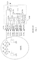
- Figure 1 schematically shows a pad 1000 of known type and comprising terminals or pins 16PA - 25PA and an input-output terminal 70PA adapted to be connected, by a bonding wire, to a pin (not shown) of the integrated circuit package associated with the pad 1000 itself.
- pad 1000 is provided with buffers 28PA and 30PA, an analog switch 29PA and gates 33PA and 34PA. Moreover, pad 1000 is provided with a pull-up resistor R1PA and pull-down resistor R2PA enabling to adapt electrical currents and voltages which involve the pad 1000 to values predicted for the integrated circuit to which is connected the pad 1000 or to the electronic circuit outside the pad 1000.
- Pins 16PA - 25PA are connected to an integrated analog, digital, logic circuit 400PA which controls or monitors pins 16PA - 25PA.
- the EWS test is performed on a semiconductor wafer before connecting the pads to the pins of the package and, moreover, it is possible to predict that all the pins of the pad have not been tested.
- the Final Test evaluates the pad after a package has been applied to the corresponding integrated circuit. The tests are performed by providing to the pins corresponding to the digital signals (16PA-19PA, 22PA, 24PA, 25PA) specific patterns of signals which should allow to detect the faults by a signal at the pin 22PA and input-output terminal 70PA.
- FIG. 1 it is shown an X-OR gate, LP1 of such tree having an input directly connected to the pin 16PA which is electrically connected to the logic circuit 400PA by interposing decoupling buffers B1-B4.
- decoupling buffers B1-B4 it is likely to detect also possible faults associated with the decoupling buffers B1-B4 by suitably monitoring the output of the tree of gates X-OR.
- the tree of X-OR gates can comprise a gate LP2 having an input connected to the pin 16PA by decoupling buffers B2-B4.
- the position of node N along the chain of buffers B1-B4 is not easily obtainable with precision during the layout step of the integrated circuit because, from a standpoint logic view, the operations of gates LP1 and LP2 are identical.
- a defect searched by the tests is of the kind of "stuck at" 0 or 1, due to this defect a given pin or point of the circuit of the pad is forcedly at a voltage value to which is associated the logic value 0 or 1, independently from its real operative condition.
- the term "detected for stuck at 0 or 1” means that always exists at least one pattern of input signals which enables to activate and propagate the fault so that the latter can be reliably detected at an exit pin.
- the term “Undetectable” means that the fault can not be determined because it is not possible to detect a pattern of input signals enabling to activate and propagate the fault so that the latter can be reliably located at an exit pin.
- Document US-A-2009-022479 describes an internal connection output pad connected to a CMOS output circuit on a first chip is electrically connected via a chip-to-chip bonding wire to an internal connection input pad connected to a CMOs input circuit on a second chip.
- a test circuit controls a high-impedance output stage, a high-level output state and a low-level output state of the internal connection output pad via the CMOS output circuit.
- the Applicant has observed that the known techniques of detecting faults can be improved because they do not guarantee a satisfying "coverage", that, is a detection of the faults.
- the object of the present invention consists of providing an interconnection device or pad which enables an improved coverage with respect to what it is possible to obtain with conventional techniques, without entailing an undue circuital complexity.
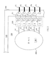
- FIG. 2 schematically illustrates an electronic apparatus 300, comprising an integrated circuit in a die of semiconductor material or chip 100, provided with a corresponding package 200.
- Chip 100 comprises a region in which it is made an integrated electronic circuit 400 such as, for example, a digital and analog logic D-A-L, and an electric interconnection region or pad region 500.
- the digital and analog logic 400 implements the functions associated with the electronic apparatus 300.
- the pad region 500 comprises a plurality of pad devices (or electrical interconnection devices) 1-5 similar to each other.
- Each pad device 1-5 is electrically connected to the digital and analog logic 400 by corresponding integrated conductive paths b1-b5 adapted to carry suitable signals. Moreover, each pad device 1-5 is provided with a corresponding bonding area 6-10 to which a corresponding conductive wire 11-15 is fixed which is connected, at the other end, to terminals or pins P1-P5 provided with corresponding bonding areas. Pins P1-P5 are adapted to receive signals outside the electronic apparatus 300 and transmit them to the outside and/or make available, outside the apparatus 300, the signals provided by the digital and analog logic 400.
- the pad devices 1-5 act as an interface between the electronic apparatus 300 and the outer apparatuses to which this apparatus is connected, enabling also to perform a suitable decoupling of the corresponding inner devices and a suitable adaptation of the involved electrical voltages.
- the pad 1 comprises, for example, a plurality of electrical terminals or pins 16-26 connected to the integrated electronic circuit 400 of Figure 2 , an adapting block 60 and an input-output terminal 70. Pins 16-26 are connected to the integrated electronic circuit 400, for example, by conductive paths b1 of Figure 2 , while the input-output terminal 70 is connected to the bonding area 6.
- the adapting block 60 moreover comprises, at least an inner electrical device and, particularly, can comprise a plurality of inner electrical devices.
- electrical devices inside the pad 1 are: an output buffer 28, a block 27 for controlling the transition rate, an analog transmission gate 29, an input buffer 30, a weak logic state driving device (for example comprising a pull-up resistor R1, a pull-down resistor R2 and a control device CR).
- the adapting block 60 is provided with at least a voltage shifter 41.
- there are other types of pads comprising further or different devices.
- the first electrical terminal 16 is adapted to receive, from the integrated electronic circuit 400, a transition rate control digital signal ipp_sre (slew rate controller) capable of taking the logic value 0 or the logic value 1.
- the first electrical terminal 16 is connected to the transition rate control block 27 for supplying to the latter the transition rate control signal ipp_sre which adjusts its operation.
- a second input terminal 17 is adapted to receive, from the integrated electronic circuit 400, an output buffer enable signal ipp_obe capable of taking the logic value 0 or 1.
- the second electrical terminal 17 is connected to the output buffer 28 (particularly, a tristate buffer) for supplying to the latter the buffer enable signal ipp_obe capable of enabling or disabling the operation of such buffer 28.
- a third input terminal 18 is adapted to receive, from the integrated electronic circuit 400, a pad input digital signal 1 (Data Output) ipp_do associated with a datum to be made available at the input-output terminal 70.
- the third input terminal 18 is connected to an input of the output buffer 28, having a corresponding output connected to an input of the rate transition control block 27.
- An output of the rate transition control block 27 is connected to the input-output terminal 70.
- the input signal ipp_do can be suitably amplified by the output buffer 28 when is active, then it can be supplied to the rate transition control block 27 which adjusts the rate of a ramp associated with the transitions from 0 to 1, and vice versa, of the input signal ipp_do.
- the fourth terminal 19 is configured for receiving, from the integrated electronic circuit 400, a digital signal analogswen for enabling or disabling the transmission gate 29 which is provided with a first input/output connected to the fifth terminal 20 and a second input/output connected, by a resistor R, to the input-output terminal 70.
- a digital signal analogswen for enabling or disabling the transmission gate 29 which is provided with a first input/output connected to the fifth terminal 20 and a second input/output connected, by a resistor R, to the input-output terminal 70.
- the fifth terminal 20 is configured to be put in connection, by the transmission gate 29 and the resistor R, with the input-output terminal 70 in order to take an electrical voltage dependent on the voltage taken at the input-output terminal 70 and therefore for transmitting or receiving an analog-type signal.
- the sixth terminal 21 is configured for receiving, from the integrated electronic circuit 400, an input buffer enabling digital signal ipp_ibe adapted to selectively take logic values 0 and 1 in order to enable (for example, for the logic value 1) and disable the input buffer 30 (for example, for the logic value 0).
- the seventh terminal 22 is connected to an exit of the input buffer 30 which is provided with an input connected to a node 31 in turn connected, by the resistor R, to the input-output terminal 70.
- the node 31 is also connected to the second input/output of the transmission gate 29.
- an output digital signal ipp_ind corresponding to the one present at the input-output terminal 70.
- the signal at the seventh terminal 22 takes a value independent of the input-output signal 70.
- the eighth terminal 23 is configured for receiving from the input-output terminal 70, to which it is connected by the node 31 and resistor R, an input analog signal ipp_ina to be used for directly transmitting or receiving the analog signal present at the input-output terminal 70.
- the pull-up resistor R1 is connected between a supplying terminal Vdd and a first node 32, interposed between the resistor R and node 31.
- the pull-down resistor R2 is connected between the ground terminal GND and the first node 32.
- Each pull-up R1 and pull-down R2 resistors is implemented, for example, by one or more MOSFET (Metal Oxide Semiconductor Field Effect Transistor) transistors which can be activated or deactivated by corresponding drive signals from the control device CR.
- MOSFET Metal Oxide Semiconductor Field Effect Transistor
- the pull-up resistor R1 can be a P-channel MOSFET while the pull-down R2 can be a N-channel MOSFET.
- the control device CR comprises a first NAND gate 33 and a second AND gate 34.
- the first NAND gate 33 is provided with a first input connected to a second node 35, in turn connected to a ninth terminal 24, and a second input connected to a third node 36.
- the ninth terminal 24 is configured for receiving a selection digital signal ipp_pus.
- An output of the first NAND gate 33 is connected to the pull-up resistor R1.
- the second AND gate 34 is provided with a corresponding first inverting input connected to the second node 35 and a second input connected to the third node 36.
- the third node 36 is connected to the tenth terminal 25 which is configured for receiving a further enabling digital signal ipp_pue.
- the enabling digital signal ipp_pue when the enabling digital signal ipp_pue takes the value 0, no pull-up R1 and pull-down resistors R2 is enabled.
- the first voltage translator 41 is connected between the first terminal 16 and the rate transition control block 27 and enables to suitably raise the electrical voltage associated with the rate transition control signal ipp_sre.
- the second 17, third 18, fourth 19, sixth 21, seventh 22, ninth 24, tenth 25 terminals are provided with a corresponding voltage translator 42-48 inside the adaptation block 60.
- symbol “ ⁇ ” means that the corresponding level translator performs an increase of the electrical voltage between its input and its output while the symbol “ ⁇ ” means that the corresponding level translator performs a decrease of the electrical voltage between its input and output.
- the pad 1 is also provided with a fault detecting logic module 50 ( Figure 4 ) which, according to the example shown also in Figure 3 , comprises at least one input connected to an output of one of the electrical devices inside the adapting block 60 and that is inside the pad 1 itself.
- the fault detecting logic module 50 ( Figure 4 ) is integrated inside the pad 1.
- the fault detecting logic module 50 can be a combinatorial network comprising a plurality of gates.
- the fault detecting logic module 50 which withdraws digital signals, comprises X-OR gates that is gates for which is provided an output of value 1 if the number of logic values 1 present at its inputs is odd.
- the fault detecting logic module 50 can comprise other types of gates such as, for example, AND, NAND, NOT, OR, NOR gates, etc., combined in a different way from what is shown in the figures.
- the fault detecting logic module 50 is provided with a first X-OR gate 51, second X-OR gate 52, third X-OR gate 53 and a fourth X-OR gate 54.
- the first gate 51 is provided with a first input 55 connected at the output of the first voltage translator 41 associated with the first terminal 16, a second input 56 connected at the output of a second voltage translator 42 associated with the second terminal 17, a third input 57 connected at the output of a third voltage translator 43 and associated with the third terminal 18.
- the output of the first gate 51 leads to an input of the fourth gate 54.
- the second gate 52 is provided with: a fourth input 58 connected to the output of a fourth level translator 44 associated with the fourth terminal 19, a fifth input 59 connected at the output of a sixth level translator 46 and associated with a seventh terminal 22, and a sixth input 61 connected at the output of a fifth level translator 45 associated with the sixth terminal 21.
- the output of the second gate 52 leads to a further input of the fourth gate 54.
- the third gate 53 is provided of: a seventh input 62 connected at the output of the first NAND gate 33, an eight input 63 connected at the output of the second AND gate 34.
- the output of the third gate 53 leads to a further input of the fourth gate 54.
- the fourth gate 54 combines the signals at its inputs and is provided with an output connected, by a ninth level translator 49, (only shown in Figure 3 and performing a downward translation) to the detecting terminal 26, adapted to supply a detecting signal ipp_xor indicative of the result of a test performed at the pad 1.
- the digital and analog logic 400 (D-A-L) is provided with a test managing block 80 addressing, among other things, the managing of the detecting signal ipp_xor for monitoring the logic state, for example, by an acquisition flip-flop.
- the fault detecting module 50 which is integrated inside the pad 1, can be used for detecting the presence of a fault in the pad 1 and also the presence of faults of a digital part of the digital and analog logic 400.
- the possibility of detecting both faults of a digital portion of the digital and analog logic 400 and faults inside the pad 1 is particularly advantageous with reference to the approach of the prior art shown in Figure 1 , according to it the X-OR tree can be used only for detecting the faults associated with the control logic 400PA.
- the detecting module 50 can be used also for diagnostic operations of the pad having the purpose of detecting specific terminals on which the faults are present.
- the pad of Figure 3 can be implemented by conventional techniques of integration of electronic circuits in chip of semiconductor material.
- the pad of Figure 3 in comparison with the digital and analog logic 400 (particularly its digital portion) is a so-called hard block, that is, it is designed one time and used as is without being modified.
- the so-called stuck-at faults causing the digital terminals of the plurality 16-25 or other points of pad 1 to behave as if they had a fixed voltage value independently of the forced value that it should be predicted for their correct operation.
- the faults can be found by different test steps to be performed by the pad 1.
- Some of such conventional test steps are: the EWS, Electrical Wafer Sort and Final Test.
- the EWS test operates on all or some of pads 1-5 without the bonding connection to the pins P1-P5 of the package 200.
- the Final Test operates on all or some of the pads provided of the relative bonding connection to the pins P1-P5.
- test machine (not shown and known per se) that is connected to the pins P1-P5 of the electronic apparatus 300 of Figure 2 and that suitably configures both the digital and analog logic 400 and the test managing block 80.
- the test machine is connected to the bonding areas 6-10.
- the tests are performed by applying to the terminals 16-25 and input-output terminal 70 a combination of signals and reading the corresponding result at the detecting terminal 26 by the test managing block 80.
- the managing block 80 signals the fault to the test machine directly by a pad dedicated to this operation or by a "scan structure".
- the scan structure is an architecture comprised in the digital and analog logic 400 which causes the logic 400 to be configured as a shift register and is used by the tool ATGP for generating test patterns.
- the test patterns can be obtained by using tools enabling the automatic generation of inspecting patterns commonly indicated by the acronym ATPG, Automatic Test Pattern Generation.
- a fault is classified as "detected" when it is possible to apply a pattern to which corresponds at least an exit signal examinable, without uncertainties, of the circuit undergoing the test which is different from the one obtainable by applying the same pattern to a circuit free of faults and used as a reference.
- a fault is classified as "Undetectable by ATPG" when the ATPG test is not capable of detecting the fault.
- a fault is classified as "Parametric detected” when can be detected only by a parametric measurement of the concerned electrical quantities, such as electrical voltages or currents different from the conventional logic states 0 and 1 at the input-output terminal 70.
- a fault is classified as "Possible detected" when it is possible to apply a pattern to which corresponds at least an observable output signal, but with uncertainties, of the circuit undergoing the test which is different from the one obtainable by applying the same pattern to a circuit free of faults and used as reference.
- the detection of this fault is possible but non-deterministic and can be detected with a probability of 50%.
- a fault is defined as "detected rely on pull drivers" when the certainty is less than the "detected” classification because there is a dependence on the voltage values due to the pull-up and pull-down resistors, R1 and R2, which make less certain the distinction between the detected values.
- the fault classification With reference to the stuck-at 0/1 faults, the fault classification with reference to each terminal of the group 16-19, 21-22 and 24-25 affected by digital signals, depends on both the circuitry connected to the terminal itself and the type of connection of the fault detecting module 50 integrated in the pad 1.
- Table 1 it is shown the classification of faults of the pad 1 for the digital terminals 16-19 and 21, 22, 24, 25 and of the input-output terminal 70 of Figure 1 .
- Table 1 ( Figures 3 and 4 ) Terminal Bounded stuck at 0/1 No. Unbounded stuck at 0/1 16 Detected 17 Detected 18 Detected 19 Detected 21 Detected 22 Detected 24 Detected 25 Detected 70 Bounded stuck at 0/1: detected Unbounded stuck at 0/1: undetectable by ATPG
- Table 2 In the following it is reported Table 2 in which the faults classifications are indicated for a pad circuit 1000 according to the prior art, shown in Figure 1 , and evaluated according to the methodology ATPG.
- Table 2 (prior art, Figure 1 ) Terminal Bounded stuck at 0/1 Unbounded stuck at 0/1 16PA Undetectable by ATPG detected rely on pull drivers or possible detected 17PA 18PA detected 19PA undetectable by APTG 21PA detected 22PA detected 24PA Detected rely on pull drivers or possible detected 25PA Bounded stuck at 0/1: parametric detected Unbounded stuck at 0/1: possible detected 70PA Bounded stuck at 0/1: detected Unbounded stuck at 0/1: undetectable by ATPG
- enabling digital signal ipp_pue When such enabling signal ipp_pue is at value 1, it enables the pull-up resistor R1PA or pull-down resistor R2PA as a function of the value of the selection digital signal ipp_pue (1 ⁇ pull-up and 0 ⁇ pull-down).
- the terminal 25PA (terminal corresponding to the enabling signal ipp_pue) is forced to value 1, that is the value opposed to that of the stuck-at fault, suitably configuring the digital and analog logic 400, for example, by the above described scan structure.
- the pull-up resistor R1PA is activated.
- the buffer enabling signal ipp_obe is forced to 0.
- the output buffer 28PA is turned off, the outer driver applied to the input-output terminal 70PA has a high impedance so the output-input terminal 70PA takes a voltage value Vdd (equivalent to a logic state 1) due to the turning on of the pull-up resistor R1PA.
- the fault can be considered Possible Detected because in case wherein X (which is not a physical value, but a logic state used during the modelling) equals 0, the fault is detected (it was expected 1 from a circuit free of fault) while in case wherein equals 1, the fault is considered undetected. It should be mentioned that, as a convention, a fault is defined as Possible Detected if it has a probability to be detected of 50%.
- the fault is classified as detected thanks to the presence of the fault detecting module 50 which is used for detecting the faults of the pad 1 itself. Particularly, at the third gate 53 which is connected to the output of gates 33 and 34. A fault of the tenth terminal 25 or one of these gates 33 and 34, is highlighted by the value taken by the detecting signal ipp_xor present at the detecting terminal 26 and is observed by the test block 80.
- the fault detecting module 50 due to the fact its inputs are directly connected to the output of specific devices inside the pad 1, will take to a detecting signal ipp_xor present at the detecting terminal 26 which will be also influenced by the behaviour of the inner devices, providing therefore a more complete coverage of the faults.
- the fault detecting module 50 enables to detect, not only the stuck-at faults but also the transient faults, bound to the presence of delays introduced, for example, by some level translators 41-49.
- the present of inputs of the gates of the fault detecting module 50 downstream a level translator enables to evaluate the presence of an undesired delay caused by it.
- FIG 5 it is shown a further embodiment of the pad 1, used in the electronic apparatus 300 of Figure 2 , similar to that of the pad 1 shown in Figure 3 .
- a multiplexer 37 having a corresponding first input 38 connected to the output of the output buffer 30 and a corresponding second input 39 for receiving the output of the fourth gate 54 of the fault detecting module 50 is used.
- An output of the multiplexer 37 is connected to the seventh terminal 22 and the multiplexer 37 is provided with an input for a selection digital signal ipp_tst to be supplied by the integrated electronic circuit 400 to a selection terminal ADD-PAD.
- the multiplexer 37 will supply to the seventh terminal 22 the input digital signal ipp_ind from the output buffer 30 or the detecting signal ipp_xor from the fourth gate 54.
- the same Table 1 corresponding to the classification of faults referring to the pad itself is also valid.
- the value of the test selection digital signal ipp_ tst is forced so that it assumes a logic value which enables the propagation of the signal present at the first input 38, while during the test pattern generation by, for example, ATPG and the following activation of the scan structure, such signal ipp_tst can take selectively both the logic values.
- the embodiment shown in Figure 5 is advantageous because its design is not complex and moreover it does not need a test managing block 80 requiring a complex design because it is not necessary to monitor the signal exiting the fault detecting module 50, but it is just necessary that it is capable of controlling the multiplexer 37, for example, by generating suitable values of the selection digital signal test ipp_tst.
Landscapes
- Engineering & Computer Science (AREA)
- General Engineering & Computer Science (AREA)
- Physics & Mathematics (AREA)
- General Physics & Mathematics (AREA)
- Semiconductor Integrated Circuits (AREA)
- Tests Of Electronic Circuits (AREA)
Claims (16)
- Dispositif de plot intégré d'interconnexion électrique (1) comprenant :une pluralité de bornes électriques (16-26) intégrées sur une région de plot (500) d'une puce (100) et pouvant être connectées à un circuit électronique intégré (400) intégré sur ladite puce (100) partagée avec ledit dispositif de plot intégré d'interconnexion électrique (1), le circuit électronique intégré (400) étant externe au dispositif de plot intégré d'interconnexion électrique (1) ;un bloc d'adaptation (60) intégré dans ladite région de plot (500) et comprenant au moins un dispositif électrique interne (43 ; 33 ; 34) comportant une entrée correspondante connectée à une première borne (18 ; 24 ; 25) de ladite pluralité de bornes électriques et une sortie correspondante (57 ; 62 ; 63) ;un module de logique de détection de défaut (50) ayant une première entrée (57 ; 62 ; 63) connectée à ladite sortie (57 ; 62 ; 63) de l'au moins un dispositif électrique interne (43 ; 33 ; 34) pour recevoir un signal numérique et comportant une borne de détection (26 ; 22) pour fournir un signal de détection de défaut (ipp_xor) représentant un défaut détecté dans le dispositif de plot intégré d'interconnexion électrique (1) ; etau moins une borne d'entrée/sortie (70) pouvant être connectée électriquement à ladite pluralité de bornes électriques (16-26) par l'intermédiaire dudit bloc d'adaptation (60) et à connecter à un dispositif électrique externe.
- Dispositif de plot d'interconnexion selon la revendication 1, dans lequel le module de logique de détection de défaut (50) comprend un réseau combinatoire.
- Dispositif de plot d'interconnexion (1) selon la revendication 2, dans lequel le module de logique de détection de défaut (50) comprend une pluralité de portes comprenant une porte de sortie configurée pour délivrer le signal de détection de défaut (ipp_xor).
- Dispositif de plot d'interconnexion (1) selon la revendication 3, dans lequel ladite pluralité de portes comprend une pluralité de portes OU exclusif.
- Dispositif de plot d' interconnexion selon au moins l'une des revendications précédentes, dans lequel ledit module de logique de détection de défaut (50) est configuré pour détecter des défauts bloqué du dispositif de plot (1).
- Dispositif de plot d'interconnexion (1) selon au moins la revendication 5, dans lequel ledit au moins un dispositif électrique interne comprend :un dispositif de pilotage d'état logique (R1 ;
R2) associé à ladite borne d'entrée/sortie (70) ;un module de commande (CR, 33, 34) dudit dispositif de pilotage comportant une première borne d'entrée (25) connectée à une borne de ladite pluralité de bornes pour recevoir un signal d'activation (ipp_pue) du dispositif de pilotage (R1, R2) et un signal de sortie (62, 63) connecté audit dispositif de pilotage et audit module de détection de défaut (50). - Dispositif de plot d'interconnexion (1) selon au moins l'une des revendications précédentes, dans lequel le module de détection de défaut est agencé pour être utilisé dans une étape de test du dispositif d'interconnexion.
- Dispositif de plot d'interconnexion (1) selon au moins la revendication 5, comprenant en outre :un tampon de sortie (28) ayant une entrée respective connectée à une seconde borne (18) de ladite pluralité et à une seconde entrée (57) du module de détection de défaut (50) ;un dispositif de commande de vitesse de transition (27) d'un signal de sortie dudit tampon de sortie ayant une entrée de pilotage connectée à une troisième entrée (55) du module de détection de défaut (50) et une première sortie connectée à ladite borne d'entrée/sortie (70).
- Dispositif de plot d'interconnexion (1) selon au moins la revendication 5, comprenant en outre :un tampon d'entrée (30) ayant une entrée de données (31) connectée à ladite au moins une borne d'entrée/sortie (70) par une résistance (R) et une sortie de données connectée à une troisième borne (22) de ladite pluralité ; le module de détection de défaut comportant une quatrième entrée (59) connectée à la troisième borne (22) de ladite pluralité.
- Dispositif de plot d'interconnexion (1) selon la revendication 1, dans lequel ledit au moins un dispositif électrique interne comprend au moins un traducteur de tension (41-48).
- Dispositif de plot d'interconnexion (1) selon au moins la revendication 1, dans lequel le module de détection de défaut (50) est configuré pour détecter des défauts dans des configurations de valeur numérique fournies à ladite pluralité de bornes.
- Dispositif de plot d'interconnexion (1) selon au moins la revendication 9, comprenant en outre un multiplicateur (37) ayant :un premier port d'entrée connecté à la sortie de données dudit tampon d'entrée (30) ;un second port d'entrée connecté à la borne de détection pour recevoir le signal de détection de défaut (ipp_xor) ;un port de sortie connecté à la troisième borne (22) de ladite pluralité ;une entrée de sélection (ADD-PAD) pour un signal de sélection de test (ipp_tst) agencé pour connecter sélectivement le port de sortie au premier ou second port d'entrée.
- Appareil électronique (300), comprenant :un circuit intégré sur une puce de matériau semiconducteur (100) comprenant :une zone comprenant un circuit électronique intégré (400),une région de plot comprenant au moins un dispositif de plot d'interconnexion électrique (1-5) ;
un boîtier (200) dudit circuit intégré (100) ;dans lequel ledit dispositif de plot d'interconnexion électrique (1-5) est mis en oeuvre selon au moins l'une des revendications précédentes. - Appareil électronique (300) selon la revendication 13, dans lequel un bloc de circuit de test (80) configuré pour gérer ledit signal de détection de défaut est mis en oeuvre dans ledit circuit électronique intégré (400).
- Appareil électronique (300) selon les revendications 12 et 13, dans lequel ledit circuit électronique intégré (400) comprend un bloc de circuit de test (80) configuré pour commander ledit multiplicateur (37).
- Appareil électronique (300) selon la revendication 14 ou la revendication 15, dans lequel ledit module de détection de défaut est configuré et connecté électriquement audit dispositif de plot d'interconnexion également pour détecter des défauts du circuit électronique intégré (400).
Applications Claiming Priority (1)
| Application Number | Priority Date | Filing Date | Title |
|---|---|---|---|
| ITMI20100151 | 2010-02-02 |
Publications (2)
| Publication Number | Publication Date |
|---|---|
| EP2362233A1 EP2362233A1 (fr) | 2011-08-31 |
| EP2362233B1 true EP2362233B1 (fr) | 2014-05-14 |
Family
ID=42671905
Family Applications (1)
| Application Number | Title | Priority Date | Filing Date |
|---|---|---|---|
| EP11152184.5A Active EP2362233B1 (fr) | 2010-02-02 | 2011-01-26 | Dispositif intégré d'interconnexion électrique doté d'un module de détection des fautes et appareil électronique comprenant le dispositif |
Country Status (2)
| Country | Link |
|---|---|
| US (1) | US8618812B2 (fr) |
| EP (1) | EP2362233B1 (fr) |
Families Citing this family (4)
| Publication number | Priority date | Publication date | Assignee | Title |
|---|---|---|---|---|
| WO2017207352A1 (fr) * | 2016-06-01 | 2017-12-07 | Philips Lighting Holding B.V. | Détection d'erreur sur des broches d'entrée/sortie de circuit intégré |
| EP3465239B1 (fr) | 2016-06-01 | 2020-05-20 | Signify Holding B.V. | Circuit intégré de détection d'erreur sur des broches d'entrée/sortie |
| CN111398794B (zh) * | 2020-03-31 | 2022-07-15 | 苏州汇川技术有限公司 | 数字量输入信号检测电路及电梯控制器 |
| CN114895614B (zh) * | 2022-07-14 | 2022-10-11 | 天津飞旋科技股份有限公司 | 一种可编程控制器 |
Family Cites Families (11)
| Publication number | Priority date | Publication date | Assignee | Title |
|---|---|---|---|---|
| GB2204693B (en) * | 1987-05-14 | 1991-02-13 | Rolls Royce Plc | Turbomachine tip clearance sensor |
| GB2229004B (en) * | 1989-03-07 | 1993-09-29 | Rolls Royce Plc | Improvements in or relating to gas turbine engine tip clearance sensors |
| US5552711A (en) * | 1994-11-10 | 1996-09-03 | Deegan; Thierry | Turbine engine imminent failure monitor |
| US5818242A (en) * | 1996-05-08 | 1998-10-06 | United Technologies Corporation | Microwave recess distance and air-path clearance sensor |
| US6889368B1 (en) * | 2002-10-25 | 2005-05-03 | Xilinx, Inc. | Method and apparatus for localizing faults within a programmable logic device |
| US7516237B2 (en) * | 2003-08-20 | 2009-04-07 | Intel Corporation | Scalable device-to-device interconnection |
| US7095221B2 (en) * | 2004-05-27 | 2006-08-22 | Siemens Aktiengesellschaft | Doppler radar sensing system for monitoring turbine generator components |
| FR2897439A1 (fr) * | 2006-02-15 | 2007-08-17 | St Microelectronics Sa | Circuit elelctronique comprenant un mode de test securise par l'utilisation d'un identifiant, et procede associe |
| JPWO2007097053A1 (ja) * | 2006-02-23 | 2009-07-09 | パナソニック株式会社 | 半導体集積回路とその検査方法 |
| US7814386B2 (en) * | 2007-10-31 | 2010-10-12 | Texas Instruments Incorporated | Built in self test for input/output characterization |
| US8449255B2 (en) * | 2010-03-21 | 2013-05-28 | Btpatent Llc | Wind turbine blade system with air passageway |
-
2011
- 2011-01-26 EP EP11152184.5A patent/EP2362233B1/fr active Active
- 2011-02-02 US US13/019,790 patent/US8618812B2/en active Active
Also Published As
| Publication number | Publication date |
|---|---|
| US20110187384A1 (en) | 2011-08-04 |
| EP2362233A1 (fr) | 2011-08-31 |
| US8618812B2 (en) | 2013-12-31 |
Similar Documents
| Publication | Publication Date | Title |
|---|---|---|
| US8225156B1 (en) | Methods and apparatuses for external voltage test methodology of input-output circuits | |
| US5115191A (en) | Testing integrated circuit capable of easily performing parametric test on high pin count semiconductor device | |
| US6397361B1 (en) | Reduced-pin integrated circuit I/O test | |
| US7301836B1 (en) | Feature control circuitry for testing integrated circuits | |
| US6762614B2 (en) | Systems and methods for facilitating driver strength testing of integrated circuits | |
| US20060248419A1 (en) | Methods and apparatus for extending semiconductor chip testing with boundary scan registers | |
| US8779790B2 (en) | Probing structure for evaluation of slow slew-rate square wave signals in low power circuits | |
| US11454669B2 (en) | Circuit for detecting damage to a peripheral edge on an integrated circuit die | |
| US6844624B1 (en) | Multichip module | |
| US20130141124A1 (en) | Test method of driving apparatus and circuit testing interface thereof | |
| WO2007097053A1 (fr) | Circuit integre a semi-conducteurs et son procede d'inspection | |
| EP2362233B1 (fr) | Dispositif intégré d'interconnexion électrique doté d'un module de détection des fautes et appareil électronique comprenant le dispositif | |
| CN103383416B (zh) | 测试片外驱动器的阻抗的电路与方法 | |
| US5936423A (en) | Semiconductor IC with an output circuit power supply used as a signal input/output terminal | |
| US8169230B2 (en) | Semiconductor device and method of testing the same | |
| US6260163B1 (en) | Testing high I/O integrated circuits on a low I/O tester | |
| US6876218B1 (en) | Method for accurate output voltage testing | |
| US5796260A (en) | Parametric test circuit | |
| US6275055B1 (en) | Semiconductor integrated circuit | |
| US11313904B2 (en) | Testing device and testing method | |
| US7230446B2 (en) | Semiconductor logic circuit device having pull-up/pull-down circuit for input buffer pad and wafer-probing testing method therefor | |
| JP2005072375A (ja) | 半導体集積回路 | |
| EP1224481B1 (fr) | Dispositif et technique de commutation parametrique programmable pour plages numeriques a technologie cmos | |
| KR0157900B1 (ko) | 집적 회로내의 입출력 장치 | |
| US7552372B2 (en) | Semiconductor device and test method thereof |
Legal Events
| Date | Code | Title | Description |
|---|---|---|---|
| PUAI | Public reference made under article 153(3) epc to a published international application that has entered the european phase |
Free format text: ORIGINAL CODE: 0009012 |
|
| AK | Designated contracting states |
Kind code of ref document: A1 Designated state(s): AL AT BE BG CH CY CZ DE DK EE ES FI FR GB GR HR HU IE IS IT LI LT LU LV MC MK MT NL NO PL PT RO RS SE SI SK SM TR |
|
| AX | Request for extension of the european patent |
Extension state: BA ME |
|
| 17P | Request for examination filed |
Effective date: 20120223 |
|
| RAP1 | Party data changed (applicant data changed or rights of an application transferred) |
Owner name: STMICROELECTRONICS SRL |
|
| 17Q | First examination report despatched |
Effective date: 20120831 |
|
| GRAP | Despatch of communication of intention to grant a patent |
Free format text: ORIGINAL CODE: EPIDOSNIGR1 |
|
| INTG | Intention to grant announced |
Effective date: 20140108 |
|
| GRAS | Grant fee paid |
Free format text: ORIGINAL CODE: EPIDOSNIGR3 |
|
| GRAA | (expected) grant |
Free format text: ORIGINAL CODE: 0009210 |
|
| AK | Designated contracting states |
Kind code of ref document: B1 Designated state(s): AL AT BE BG CH CY CZ DE DK EE ES FI FR GB GR HR HU IE IS IT LI LT LU LV MC MK MT NL NO PL PT RO RS SE SI SK SM TR |
|
| REG | Reference to a national code |
Ref country code: GB Ref legal event code: FG4D |
|
| REG | Reference to a national code |
Ref country code: AT Ref legal event code: REF Ref document number: 668677 Country of ref document: AT Kind code of ref document: T Effective date: 20140615 |
|
| REG | Reference to a national code |
Ref country code: DE Ref legal event code: R096 Ref document number: 602011006840 Country of ref document: DE Effective date: 20140618 Ref country code: IE Ref legal event code: FG4D |
|
| REG | Reference to a national code |
Ref country code: AT Ref legal event code: MK05 Ref document number: 668677 Country of ref document: AT Kind code of ref document: T Effective date: 20140514 Ref country code: NL Ref legal event code: VDEP Effective date: 20140514 |
|
| REG | Reference to a national code |
Ref country code: LT Ref legal event code: MG4D |
|
| PG25 | Lapsed in a contracting state [announced via postgrant information from national office to epo] |
Ref country code: IS Free format text: LAPSE BECAUSE OF FAILURE TO SUBMIT A TRANSLATION OF THE DESCRIPTION OR TO PAY THE FEE WITHIN THE PRESCRIBED TIME-LIMIT Effective date: 20140914 Ref country code: GR Free format text: LAPSE BECAUSE OF FAILURE TO SUBMIT A TRANSLATION OF THE DESCRIPTION OR TO PAY THE FEE WITHIN THE PRESCRIBED TIME-LIMIT Effective date: 20140815 Ref country code: LT Free format text: LAPSE BECAUSE OF FAILURE TO SUBMIT A TRANSLATION OF THE DESCRIPTION OR TO PAY THE FEE WITHIN THE PRESCRIBED TIME-LIMIT Effective date: 20140514 Ref country code: NO Free format text: LAPSE BECAUSE OF FAILURE TO SUBMIT A TRANSLATION OF THE DESCRIPTION OR TO PAY THE FEE WITHIN THE PRESCRIBED TIME-LIMIT Effective date: 20140814 Ref country code: CY Free format text: LAPSE BECAUSE OF FAILURE TO SUBMIT A TRANSLATION OF THE DESCRIPTION OR TO PAY THE FEE WITHIN THE PRESCRIBED TIME-LIMIT Effective date: 20140514 Ref country code: FI Free format text: LAPSE BECAUSE OF FAILURE TO SUBMIT A TRANSLATION OF THE DESCRIPTION OR TO PAY THE FEE WITHIN THE PRESCRIBED TIME-LIMIT Effective date: 20140514 |
|
| PG25 | Lapsed in a contracting state [announced via postgrant information from national office to epo] |
Ref country code: HR Free format text: LAPSE BECAUSE OF FAILURE TO SUBMIT A TRANSLATION OF THE DESCRIPTION OR TO PAY THE FEE WITHIN THE PRESCRIBED TIME-LIMIT Effective date: 20140514 Ref country code: PL Free format text: LAPSE BECAUSE OF FAILURE TO SUBMIT A TRANSLATION OF THE DESCRIPTION OR TO PAY THE FEE WITHIN THE PRESCRIBED TIME-LIMIT Effective date: 20140514 Ref country code: AT Free format text: LAPSE BECAUSE OF FAILURE TO SUBMIT A TRANSLATION OF THE DESCRIPTION OR TO PAY THE FEE WITHIN THE PRESCRIBED TIME-LIMIT Effective date: 20140514 Ref country code: ES Free format text: LAPSE BECAUSE OF FAILURE TO SUBMIT A TRANSLATION OF THE DESCRIPTION OR TO PAY THE FEE WITHIN THE PRESCRIBED TIME-LIMIT Effective date: 20140514 Ref country code: SE Free format text: LAPSE BECAUSE OF FAILURE TO SUBMIT A TRANSLATION OF THE DESCRIPTION OR TO PAY THE FEE WITHIN THE PRESCRIBED TIME-LIMIT Effective date: 20140514 Ref country code: LV Free format text: LAPSE BECAUSE OF FAILURE TO SUBMIT A TRANSLATION OF THE DESCRIPTION OR TO PAY THE FEE WITHIN THE PRESCRIBED TIME-LIMIT Effective date: 20140514 Ref country code: RS Free format text: LAPSE BECAUSE OF FAILURE TO SUBMIT A TRANSLATION OF THE DESCRIPTION OR TO PAY THE FEE WITHIN THE PRESCRIBED TIME-LIMIT Effective date: 20140514 |
|
| PG25 | Lapsed in a contracting state [announced via postgrant information from national office to epo] |
Ref country code: PT Free format text: LAPSE BECAUSE OF FAILURE TO SUBMIT A TRANSLATION OF THE DESCRIPTION OR TO PAY THE FEE WITHIN THE PRESCRIBED TIME-LIMIT Effective date: 20140915 |
|
| PG25 | Lapsed in a contracting state [announced via postgrant information from national office to epo] |
Ref country code: CZ Free format text: LAPSE BECAUSE OF FAILURE TO SUBMIT A TRANSLATION OF THE DESCRIPTION OR TO PAY THE FEE WITHIN THE PRESCRIBED TIME-LIMIT Effective date: 20140514 Ref country code: SK Free format text: LAPSE BECAUSE OF FAILURE TO SUBMIT A TRANSLATION OF THE DESCRIPTION OR TO PAY THE FEE WITHIN THE PRESCRIBED TIME-LIMIT Effective date: 20140514 Ref country code: BE Free format text: LAPSE BECAUSE OF FAILURE TO SUBMIT A TRANSLATION OF THE DESCRIPTION OR TO PAY THE FEE WITHIN THE PRESCRIBED TIME-LIMIT Effective date: 20140514 Ref country code: DK Free format text: LAPSE BECAUSE OF FAILURE TO SUBMIT A TRANSLATION OF THE DESCRIPTION OR TO PAY THE FEE WITHIN THE PRESCRIBED TIME-LIMIT Effective date: 20140514 Ref country code: EE Free format text: LAPSE BECAUSE OF FAILURE TO SUBMIT A TRANSLATION OF THE DESCRIPTION OR TO PAY THE FEE WITHIN THE PRESCRIBED TIME-LIMIT Effective date: 20140514 Ref country code: RO Free format text: LAPSE BECAUSE OF FAILURE TO SUBMIT A TRANSLATION OF THE DESCRIPTION OR TO PAY THE FEE WITHIN THE PRESCRIBED TIME-LIMIT Effective date: 20140514 |
|
| REG | Reference to a national code |
Ref country code: DE Ref legal event code: R097 Ref document number: 602011006840 Country of ref document: DE |
|
| PG25 | Lapsed in a contracting state [announced via postgrant information from national office to epo] |
Ref country code: NL Free format text: LAPSE BECAUSE OF FAILURE TO SUBMIT A TRANSLATION OF THE DESCRIPTION OR TO PAY THE FEE WITHIN THE PRESCRIBED TIME-LIMIT Effective date: 20140514 |
|
| PLBE | No opposition filed within time limit |
Free format text: ORIGINAL CODE: 0009261 |
|
| STAA | Information on the status of an ep patent application or granted ep patent |
Free format text: STATUS: NO OPPOSITION FILED WITHIN TIME LIMIT |
|
| 26N | No opposition filed |
Effective date: 20150217 |
|
| PG25 | Lapsed in a contracting state [announced via postgrant information from national office to epo] |
Ref country code: IT Free format text: LAPSE BECAUSE OF FAILURE TO SUBMIT A TRANSLATION OF THE DESCRIPTION OR TO PAY THE FEE WITHIN THE PRESCRIBED TIME-LIMIT Effective date: 20140514 |
|
| REG | Reference to a national code |
Ref country code: DE Ref legal event code: R097 Ref document number: 602011006840 Country of ref document: DE Effective date: 20150217 |
|
| PG25 | Lapsed in a contracting state [announced via postgrant information from national office to epo] |
Ref country code: SI Free format text: LAPSE BECAUSE OF FAILURE TO SUBMIT A TRANSLATION OF THE DESCRIPTION OR TO PAY THE FEE WITHIN THE PRESCRIBED TIME-LIMIT Effective date: 20140514 |
|
| REG | Reference to a national code |
Ref country code: CH Ref legal event code: PL |
|
| PG25 | Lapsed in a contracting state [announced via postgrant information from national office to epo] |
Ref country code: LU Free format text: LAPSE BECAUSE OF FAILURE TO SUBMIT A TRANSLATION OF THE DESCRIPTION OR TO PAY THE FEE WITHIN THE PRESCRIBED TIME-LIMIT Effective date: 20150126 |
|
| GBPC | Gb: european patent ceased through non-payment of renewal fee |
Effective date: 20150126 |
|
| PG25 | Lapsed in a contracting state [announced via postgrant information from national office to epo] |
Ref country code: MC Free format text: LAPSE BECAUSE OF FAILURE TO SUBMIT A TRANSLATION OF THE DESCRIPTION OR TO PAY THE FEE WITHIN THE PRESCRIBED TIME-LIMIT Effective date: 20140514 |
|
| PG25 | Lapsed in a contracting state [announced via postgrant information from national office to epo] |
Ref country code: LI Free format text: LAPSE BECAUSE OF NON-PAYMENT OF DUE FEES Effective date: 20150131 Ref country code: GB Free format text: LAPSE BECAUSE OF NON-PAYMENT OF DUE FEES Effective date: 20150126 Ref country code: CH Free format text: LAPSE BECAUSE OF NON-PAYMENT OF DUE FEES Effective date: 20150131 |
|
| REG | Reference to a national code |
Ref country code: FR Ref legal event code: ST Effective date: 20150930 |
|
| REG | Reference to a national code |
Ref country code: IE Ref legal event code: MM4A |
|
| PG25 | Lapsed in a contracting state [announced via postgrant information from national office to epo] |
Ref country code: FR Free format text: LAPSE BECAUSE OF NON-PAYMENT OF DUE FEES Effective date: 20150202 |
|
| PG25 | Lapsed in a contracting state [announced via postgrant information from national office to epo] |
Ref country code: IE Free format text: LAPSE BECAUSE OF NON-PAYMENT OF DUE FEES Effective date: 20150126 |
|
| PG25 | Lapsed in a contracting state [announced via postgrant information from national office to epo] |
Ref country code: MT Free format text: LAPSE BECAUSE OF FAILURE TO SUBMIT A TRANSLATION OF THE DESCRIPTION OR TO PAY THE FEE WITHIN THE PRESCRIBED TIME-LIMIT Effective date: 20140514 |
|
| PG25 | Lapsed in a contracting state [announced via postgrant information from national office to epo] |
Ref country code: BG Free format text: LAPSE BECAUSE OF FAILURE TO SUBMIT A TRANSLATION OF THE DESCRIPTION OR TO PAY THE FEE WITHIN THE PRESCRIBED TIME-LIMIT Effective date: 20140514 Ref country code: HU Free format text: LAPSE BECAUSE OF FAILURE TO SUBMIT A TRANSLATION OF THE DESCRIPTION OR TO PAY THE FEE WITHIN THE PRESCRIBED TIME-LIMIT; INVALID AB INITIO Effective date: 20110126 Ref country code: SM Free format text: LAPSE BECAUSE OF FAILURE TO SUBMIT A TRANSLATION OF THE DESCRIPTION OR TO PAY THE FEE WITHIN THE PRESCRIBED TIME-LIMIT Effective date: 20140514 |
|
| PG25 | Lapsed in a contracting state [announced via postgrant information from national office to epo] |
Ref country code: TR Free format text: LAPSE BECAUSE OF FAILURE TO SUBMIT A TRANSLATION OF THE DESCRIPTION OR TO PAY THE FEE WITHIN THE PRESCRIBED TIME-LIMIT Effective date: 20140514 |
|
| PG25 | Lapsed in a contracting state [announced via postgrant information from national office to epo] |
Ref country code: MK Free format text: LAPSE BECAUSE OF FAILURE TO SUBMIT A TRANSLATION OF THE DESCRIPTION OR TO PAY THE FEE WITHIN THE PRESCRIBED TIME-LIMIT Effective date: 20140514 |
|
| PG25 | Lapsed in a contracting state [announced via postgrant information from national office to epo] |
Ref country code: AL Free format text: LAPSE BECAUSE OF FAILURE TO SUBMIT A TRANSLATION OF THE DESCRIPTION OR TO PAY THE FEE WITHIN THE PRESCRIBED TIME-LIMIT Effective date: 20140514 |
|
| PGFP | Annual fee paid to national office [announced via postgrant information from national office to epo] |
Ref country code: DE Payment date: 20231219 Year of fee payment: 14 |