EP2356537B1 - Active power management - Google Patents
Active power management Download PDFInfo
- Publication number
- EP2356537B1 EP2356537B1 EP09779586.8A EP09779586A EP2356537B1 EP 2356537 B1 EP2356537 B1 EP 2356537B1 EP 09779586 A EP09779586 A EP 09779586A EP 2356537 B1 EP2356537 B1 EP 2356537B1
- Authority
- EP
- European Patent Office
- Prior art keywords
- processor
- power management
- clock
- management application
- period
- Prior art date
- Legal status (The legal status is an assumption and is not a legal conclusion. Google has not performed a legal analysis and makes no representation as to the accuracy of the status listed.)
- Active
Links
Images

Classifications
-
- G—PHYSICS
- G06—COMPUTING OR CALCULATING; COUNTING
- G06F—ELECTRIC DIGITAL DATA PROCESSING
- G06F1/00—Details not covered by groups G06F3/00 - G06F13/00 and G06F21/00
- G06F1/26—Power supply means, e.g. regulation thereof
- G06F1/32—Means for saving power
- G06F1/3203—Power management, i.e. event-based initiation of a power-saving mode
-
- G—PHYSICS
- G06—COMPUTING OR CALCULATING; COUNTING
- G06F—ELECTRIC DIGITAL DATA PROCESSING
- G06F1/00—Details not covered by groups G06F3/00 - G06F13/00 and G06F21/00
- G06F1/26—Power supply means, e.g. regulation thereof
- G06F1/32—Means for saving power
- G06F1/3203—Power management, i.e. event-based initiation of a power-saving mode
- G06F1/3234—Power saving characterised by the action undertaken
- G06F1/324—Power saving characterised by the action undertaken by lowering clock frequency
-
- G—PHYSICS
- G06—COMPUTING OR CALCULATING; COUNTING
- G06F—ELECTRIC DIGITAL DATA PROCESSING
- G06F1/00—Details not covered by groups G06F3/00 - G06F13/00 and G06F21/00
- G06F1/26—Power supply means, e.g. regulation thereof
- G06F1/32—Means for saving power
- G06F1/3203—Power management, i.e. event-based initiation of a power-saving mode
- G06F1/3234—Power saving characterised by the action undertaken
- G06F1/3296—Power saving characterised by the action undertaken by lowering the supply or operating voltage
-
- Y—GENERAL TAGGING OF NEW TECHNOLOGICAL DEVELOPMENTS; GENERAL TAGGING OF CROSS-SECTIONAL TECHNOLOGIES SPANNING OVER SEVERAL SECTIONS OF THE IPC; TECHNICAL SUBJECTS COVERED BY FORMER USPC CROSS-REFERENCE ART COLLECTIONS [XRACs] AND DIGESTS
- Y02—TECHNOLOGIES OR APPLICATIONS FOR MITIGATION OR ADAPTATION AGAINST CLIMATE CHANGE
- Y02D—CLIMATE CHANGE MITIGATION TECHNOLOGIES IN INFORMATION AND COMMUNICATION TECHNOLOGIES [ICT], I.E. INFORMATION AND COMMUNICATION TECHNOLOGIES AIMING AT THE REDUCTION OF THEIR OWN ENERGY USE
- Y02D10/00—Energy efficient computing, e.g. low power processors, power management or thermal management
Definitions
- the present invention relates to a method and system for controlling the clock frequency of a processor, in an active power management scheme.
- the present invention lies in the field of active power management (APM) which means the short term control of processor clock frequencies and core supply voltage (Vdd) to minimise power consumption in an active mode.
- Active power management is generally a fast power management component, where clock frequencies and voltages may need to be modified every few hundred microseconds. Decisions are based on short term application needs.
- EP 1462915 (Kato & Mizuyama ) is directed to an information processing apparatus, wherein a clock control judging device commands a clock controller to increase a clock frequency if a specific processing section detector has detected the start of an exclusive processing section, wherein the exclusive processing section is a section during which no other processing is received in order to execute its own processing with a higher priority.
- the clock controller is commanded by the clock control judging device to decrease the clock frequency if the specific processing section detector has detected the end of the exclusive processing section.
- Another aspect of the invention provides a power management system according to claim 10.
- Embodiments of the invention described herein are particularly suitable for an architecture where the clock frequency choice is limited by its granularity - in particular in an architecture where the clock is generated by a high frequency phase-locked- loop (PLL) output divided by a divisor.
- PLL phase-locked- loop
- the divisor is output from the power management application to the clock means.
- the power management application also determines a supply voltage for the high frequency and low frequency operating intervals. In a particularly preferred embodiment, a selection is made between first and second predetermined supply voltages for the high frequency and low frequency operating intervals respectively.
- Embodiments of the invention are particularly suitable for a processor which is running a wireless modem application to implement a soft modem.
- the MIPS (mega instructions per second) characteristic of a modem application is not flat (the average MIPS required is lower than the maximum MIPS required when some intensive activity must be completed quickly). If the clock frequency of the processor (and consequently the supply voltage), are not varied during application execution, there can be long periods of inactivity. As it is more power-efficient to do the same job at a lower clock frequency compared to doing it more quickly but at a higher clock frequency, and then going idle, the power management application described herein aims to minimise inactivity periods.
- Embodiments of the invention described herein encompass an architecture in which there are two processors, one which executes real time code with regular execution patterns such as wireless modem applications, and another which resembles a more general purpose processor.
- the invention is particularly suitable for the slot-based activity in a wireless modem when information is transmitted in a wireless communication system and needs to be processed on a slot basis.
- Such systems include GSM or UMTS systems. In such a case, a period can be aligned with a slot.
- Described embodiments of the invention provide the advantage that the speed of automatic power management (APM) switching can be very fast, less than milliseconds.
- APM automatic power management
- clock frequency is subject to two-level control inputs to vary the frequency.
- Each "mode” has an APM (execution) profile (as opposed to just a single frequency) which defines a nominal high/low speed split within the APM period: this provides initial MIPS tuning.
- the nominal high/low split is then varied on a slot-by-slot basis to provide very fine, dynamic MIPS control.
- APM voltage tracking software
- FIG. 1 a schematic block diagram of a processor architecture using active power management is shown. For clarity certain elements of Figure 1 are presented as separate blocks in the block diagram denoted by function. It will readily be appreciated that these elements may in fact be software applications run on one or more processors in the architecture.
- An active power management application (APM) 10 runs on a first processor DXPO 12.
- the APM 10 is configured to receive operating cycle information in the form of MIPS from processor DXPO 12.
- APM 10 is also configured to receive parameters defining an execution profile.
- the execution profile data is supplied to APM 10 by applications running on processor DXPO 12.
- a further processor DXP1 14 is also illustrated.
- the processor DXP1 14 has no execution profile - it is assumed to operate as a general purpose processor, and can request a required operating frequency (referred to herein a MHz) on demand.
- the processor DXPO 12 handles real-time applications of a "periodic" nature. Its clock demands are discussed in the following.
- a clock frequency control output 15 from APM 10 controls a processor clock (CLK) 16.
- CLK processor clock
- the clock 16 generates a clock signal for processor DXPO 12 and processor DXP1 14 at a frequency controlled by the APM 10.
- a voltage control output 17 from APM 10 controls a function 20 within an AVS (automatic voltage supply) function 18 which selects a supply voltage from first and second preset levels, Vdd1, Vdd2. The selected setting, Vdd1 or Vdd2 sets the supply voltage of processors DXPO 12 and DXP1 14.
- the AVS 18 has a function 22 (full path function) which sets the levels of Vdd1 and Vdd2, for example to track temperature, in addition to the select (fast path) function 20 for selecting between the individual settings.
- a function 22 full path function which sets the levels of Vdd1 and Vdd2, for example to track temperature, in addition to the select (fast path) function 20 for selecting between the individual settings.
- execution profile data is supplied to APM 10.
- the execution profile data may be supplied to APM 10 by processor DXPO 12.
- Execution profiles define how the need for clock frequency (MHz) of processor DXPO 12 changes over the entire profile timespan.
- the behaviour of processor DXPO 12 is assumed to be periodic. In this context a period is a time during which intense processing activity is required, followed by a lull.
- An example is a UMTS slot of data in a wireless communication system, a UMTS slot being 666 microseconds long. The period is assumed to be "short", which means it is not possible to change supply voltage Vdd 18 many times in a period because of the change latency and APM overhead.
- Execution profiles are mode-specific. Consequently there may be separate profiles for e.g. UMTS and GSM modes.
- the software of APM 10 allows the active profile to be changed when the wireless modem mode changes (e.g. UMTS/GSM, but also UMTS voice/UMTS high speed data.
- an execution profile is composed of two parts only: high speed (high frequency) and low speed (low frequency) intervals. It is recognized that the needs of APM 10 may not be easily expressed in terms of such a simple model, so additional flexibility is allowed: the application may ask to shorten the low frequency interval in each profile period as shown in Figure 3 and discussed below.
- An execution profile includes the following information, which may be provided to APM 10 in the form of parameters:
- the APM 10 is then able to derive further information for each execution profile based on the execution profile data supplied to it.
- the derived data may include:
- DXP1 14 In the process of selecting "granted” frequencies, required MIPS from the processor DXP1 14 can be requested (in addition to the parameters from the profile) is taken into account; in this way DXP1 can modulate a profile-based "granting procedure".
- the granted MHz for the high frequency interval will usually, i.e. under normal operating conditions, be higher than the requested MHz. This is due to the granularity of the clock 16.
- the clock signal is generated by a phase locked loop (PLL) with the frequency controlled by a divisor.
- PLL phase locked loop
- the granted MHz for the low frequency interval and the actual nominal high frequency interval length may be selected to satisfy an average MHz request. They may also take into account the granularity of the clock 16.
- the granted MHz for the high and low frequency intervals remain constant for a given mode.
- the AVS function 18 receives the granted MHz on line 15 and uses them as a reference MHz to adapt two Vdd settings, Vdd1 and Vdd2. This is explained further below.
- the granted MHz for the low frequency interval cannot be higher than the granted MHz for the high frequency interval. They are allowed to be the same. This is guaranteed by the clock frequency granting procedure.
- the length of the low frequency interval can be modified in dependence on the application (modem software) executing on the processor DXPO 12.
- the modem software is configured to allow the passing of this information to APM 10 at the commencement of each period (actually on every high frequency to low frequency transition).
- the APM 10 may then decide, if necessary, to bring forward the subsequent low frequency to high frequency transition, or to suppress the low interval completely for the current period, to give the modem software more MIPS.
- PWM Pulse Width Modulation
- Profile interval switches i.e. switches from high frequency interval to low frequency interval and vice-versa, involve modifying the clock frequency and selecting the supply voltage between Vdd1/Vdd2.
- the clock frequency is modified by changing the clock divisors sent from APM 10 to CLK 16. This configuration requires no reprogramming of the phase lock loop used to generate CLK 16, and is therefore very fast.
- Voltage change is implemented herein by programming two Vdd settings for the core voltage (full path) and switching between them using a dedicated input signal 17 (fast path). Actual programming of two Vdd settings can be done by the AVS application running on processor DXP1 14, while APM 10 just selects one of two settings using fast toggling of a dedicated hardware signal.
- Vdd 18 Because of the Vdd latency, change events of Vdd 18 are scheduled before a frequency change when changing to higher frequency and voltage to ensure that the Vdd is suitable for a higher frequency.
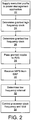
- FIG. 2 a schematic flow chart is shown outlining a sequence of steps for active power management of a processor.
- An execution profile is supplied to APM 10 at step 22.
- the execution profile comprises parameters as discussed above, and defines high frequency and low frequency operating intervals for an active period.
- APM 10 determines the granted high frequency clock (step 24) and the granted low frequency clock (step 26), taking into account MHz requirements of DXPO 12 and clock granularity. In step 28, APM passes granted clocks to AVS.
- an operating cycle requirement for the period determined by the modem software.
- the operating cycle requirement may be provided by processor DXPO 12.
- Exemplary operating cycle requirements may be in the form of required MIPS.
- the length of the low frequency interval may be calculated based on the operating cycle requirement by APM 10 at step 32.
- APM 10 determines the length of the low interval every period based on the MIPS required in this period and the actual time of the "jittery" high to low transition.
- the granted high frequency and low frequency clocks are supplied to the AVS function 18.
- the AVS may use this clock information to adapt the settings of Vdd1 and Vdd2 as described above.
- APM 10 controls CLK 16 by providing divisors to divide the clock signal provided to the phase lock loop that generates the processor clock signal.
- Vdd is controlled as explained above. Steps 30, 32, 34 are performed repeatedly in a loop.
- the APM 10 user may request dynamically (on a period by period basis) that the low frequency interval length is extended or shortened (if possible) from its nominal value depending on the estimation of its momentary clock frequency needs.
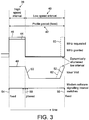
- FIG. 3 an exemplary schematic for an execution profile is shown. Time is shown on the horizontal axis. The high frequency interval 38 and the low frequency interval 40 are clearly shown as comprising the entire profile period 42.
- Figure 3 also shows the requested clock frequency 44 for the high and low frequency intervals, and the granted clock frequencies 46 for the high frequency and low frequency intervals.
- the Vdd trace 48 is also shown and demonstrates the Vdd latency 50 during transition from high frequency interval to low frequency interval, and the Vdd latency 52 during transmission from the low frequency interval to the high frequency interval.
- the start 54 of the profile period 42 and the end 56 of the profile period 42 are fixed, as already stated above. However, the transition from high frequency interval to low frequency interval may suffer from jitter 58. It can therefore be seen in Figure 3 that the length of the low frequency interval 40 may be altered 60, 62 to accommodate this and improve power efficiency by extending the low interval.
- the active power management described above is particularly suited to "periodic" software, that is for example processing slot-based data in a wireless communication system, or in other situations where the data processing is "bursty".
- the processor DXPO 12 should be allowed to request MHz in a normal manner, as the processor DXP1 14.
- the architecture can be setup so that if an execution profile is selected, any direct request from the processor DXPO 12 for MHz is ignored.
- the processor DXPO 12 could be told to "unselect" the execution profile, in which case the direct MHz request becomes valid. If no profile is selected, and neither of the processors request MHz, a minimum MHz will be selected.
- MHz requests by the processors DXP1 14 and DXPO 12 are combined in the APM 10 and passed to the AVS function 18, which tracks the supply voltage Vdd for the combined MHz request.
Landscapes
- Engineering & Computer Science (AREA)
- Theoretical Computer Science (AREA)
- Physics & Mathematics (AREA)
- General Engineering & Computer Science (AREA)
- General Physics & Mathematics (AREA)
- Power Sources (AREA)
- Mobile Radio Communication Systems (AREA)
Description
- The present invention relates to a method and system for controlling the clock frequency of a processor, in an active power management scheme.
- The present invention lies in the field of active power management (APM) which means the short term control of processor clock frequencies and core supply voltage (Vdd) to minimise power consumption in an active mode. Active power management is generally a fast power management component, where clock frequencies and voltages may need to be modified every few hundred microseconds. Decisions are based on short term application needs.
- A number of active power management schemes exist. Many such schemes which are used to find the optimum Vdd/clock frequency match assume that both parameters can be changed in a continuous manner. Such power models are not applicable in an architecture where supply voltage and/or clock frequency have a defined granularity.
-
EP 1462915 (Kato & Mizuyama ) is directed to an information processing apparatus, wherein a clock control judging device commands a clock controller to increase a clock frequency if a specific processing section detector has detected the start of an exclusive processing section, wherein the exclusive processing section is a section during which no other processing is received in order to execute its own processing with a higher priority. The clock controller is commanded by the clock control judging device to decrease the clock frequency if the specific processing section detector has detected the end of the exclusive processing section. - It is an aim of the present invention to provide a method and system for controlling the clock frequency of a processor which can alleviate the limitations which exist where a clock frequency can only be changed with granularity.
- According to one aspect of the present invention there is provided a method according to
claim 1. - Another aspect of the invention provides a power management system according to
claim 10. - Embodiments of the invention described herein are particularly suitable for an architecture where the clock frequency choice is limited by its granularity - in particular in an architecture where the clock is generated by a high frequency phase-locked- loop (PLL) output divided by a divisor. In that case, the divisor is output from the power management application to the clock means.
- In a preferred embodiment of the invention, the power management application also determines a supply voltage for the high frequency and low frequency operating intervals. In a particularly preferred embodiment, a selection is made between first and second predetermined supply voltages for the high frequency and low frequency operating intervals respectively.
- Embodiments of the invention are particularly suitable for a processor which is running a wireless modem application to implement a soft modem. The MIPS (mega instructions per second) characteristic of a modem application is not flat (the average MIPS required is lower than the maximum MIPS required when some intensive activity must be completed quickly). If the clock frequency of the processor (and consequently the supply voltage), are not varied during application execution, there can be long periods of inactivity. As it is more power-efficient to do the same job at a lower clock frequency compared to doing it more quickly but at a higher clock frequency, and then going idle, the power management application described herein aims to minimise inactivity periods.
- Embodiments of the invention described herein encompass an architecture in which there are two processors, one which executes real time code with regular execution patterns such as wireless modem applications, and another which resembles a more general purpose processor.
- The invention is particularly suitable for the slot-based activity in a wireless modem when information is transmitted in a wireless communication system and needs to be processed on a slot basis. Such systems include GSM or UMTS systems. In such a case, a period can be aligned with a slot.
- Described embodiments of the invention provide the advantage that the speed of automatic power management (APM) switching can be very fast, less than milliseconds.
- In the following embodiments, clock frequency is subject to two-level control inputs to vary the frequency.
- Each "mode" has an APM (execution) profile (as opposed to just a single frequency) which defines a nominal high/low speed split within the APM period: this provides initial MIPS tuning.
- The nominal high/low split is then varied on a slot-by-slot basis to provide very fine, dynamic MIPS control.
- A parallel, but connected voltage variation - i.e. in addition to, but partially in response to, frequency variation - gives tight interaction with voltage tracking software (AVS) to provide reliable voltage settings for both high and low portion of the APM period.
- For better understanding of the present invention and to show how the same may be carried into effect, reference will now be made by way of example to the accompanying drawings in which:
-
Figure 1 is a schematic block diagram of a processor architecture using active power management; -
Figure 2 is a schematic flow diagram of a sequence of steps for active power management in a processor; and -
Figure 3 is an exemplary schematic execution profile for a processor. - Referring to
Figure 1 a schematic block diagram of a processor architecture using active power management is shown. For clarity certain elements ofFigure 1 are presented as separate blocks in the block diagram denoted by function. It will readily be appreciated that these elements may in fact be software applications run on one or more processors in the architecture. - An active power management application (APM) 10 runs on a first processor DXPO 12. The APM 10 is configured to receive operating cycle information in the form of MIPS from processor DXPO 12. APM 10 is also configured to receive parameters defining an execution profile. In particular embodiments of the invention the execution profile data is supplied to APM 10 by applications running on processor DXPO 12. A further processor DXP1 14 is also illustrated.
- The processor DXP1 14 has no execution profile - it is assumed to operate as a general purpose processor, and can request a required operating frequency (referred to herein a MHz) on demand. The processor DXPO 12, however, handles real-time applications of a "periodic" nature. Its clock demands are discussed in the following.
- A clock
frequency control output 15 fromAPM 10 controls a processor clock (CLK) 16. Theclock 16 generates a clock signal for processor DXPO 12 and processor DXP1 14 at a frequency controlled by the APM 10. Avoltage control output 17 fromAPM 10 controls afunction 20 within an AVS (automatic voltage supply)function 18 which selects a supply voltage from first and second preset levels, Vdd1, Vdd2. The selected setting, Vdd1 or Vdd2 sets the supply voltage of processors DXPO 12 andDXP1 14. - The
AVS 18 has a function 22 (full path function) which sets the levels of Vdd1 and Vdd2, for example to track temperature, in addition to the select (fast path)function 20 for selecting between the individual settings. - In operation execution profile data is supplied to APM 10. The execution profile data may be supplied to APM 10 by processor DXPO 12.
- Execution profiles define how the need for clock frequency (MHz) of processor DXPO 12 changes over the entire profile timespan. The behaviour of processor DXPO 12 is assumed to be periodic. In this context a period is a time during which intense processing activity is required, followed by a lull. An example is a UMTS slot of data in a wireless communication system, a UMTS slot being 666 microseconds long. The period is assumed to be "short", which means it is not possible to change
supply voltage Vdd 18 many times in a period because of the change latency and APM overhead. - Execution profiles are mode-specific. Consequently there may be separate profiles for e.g. UMTS and GSM modes. The software of APM 10 allows the active profile to be changed when the wireless modem mode changes (e.g. UMTS/GSM, but also UMTS voice/UMTS high speed data.
- According to the described embodiment, an execution profile is composed of two parts only: high speed (high frequency) and low speed (low frequency) intervals. It is recognized that the needs of
APM 10 may not be easily expressed in terms of such a simple model, so additional flexibility is allowed: the application may ask to shorten the low frequency interval in each profile period as shown inFigure 3 and discussed below. - An execution profile includes the following information, which may be provided to
APM 10 in the form of parameters: - The requested clock frequency for the high frequency interval;
- The minimum length of the high frequency interval in microseconds;
- The length of the entire execution profile period; and
- The average clock frequency the application needs.
- The
APM 10 is then able to derive further information for each execution profile based on the execution profile data supplied to it. The derived data may include: - The granted clock frequency for the high frequency interval;
- The granted clock frequency for the low frequency interval; and
- The nominal high frequency interval length.
- In the process of selecting "granted" frequencies, required MIPS from the
processor DXP1 14 can be requested (in addition to the parameters from the profile) is taken into account; in this way DXP1 can modulate a profile-based "granting procedure". - The granted MHz for the high frequency interval will usually, i.e. under normal operating conditions, be higher than the requested MHz. This is due to the granularity of the
clock 16. In the described embodiment, the clock signal is generated by a phase locked loop (PLL) with the frequency controlled by a divisor. - The granted MHz for the low frequency interval and the actual nominal high frequency interval length may be selected to satisfy an average MHz request. They may also take into account the granularity of the
clock 16. - The granted MHz for the high and low frequency intervals remain constant for a given mode. The
AVS function 18 receives the granted MHz online 15 and uses them as a reference MHz to adapt two Vdd settings, Vdd1 and Vdd2. This is explained further below. - The granted MHz for the low frequency interval cannot be higher than the granted MHz for the high frequency interval. They are allowed to be the same. This is guaranteed by the clock frequency granting procedure. The length of the low frequency interval can be modified in dependence on the application (modem software) executing on the
processor DXPO 12. - That is, because the MIPS required by
processor DXPO 12 for the low frequency interval may differ on period by period basis, the modem software is configured to allow the passing of this information toAPM 10 at the commencement of each period (actually on every high frequency to low frequency transition). TheAPM 10 may then decide, if necessary, to bring forward the subsequent low frequency to high frequency transition, or to suppress the low interval completely for the current period, to give the modem software more MIPS. This feature can be viewed as a type of PWM (Pulse Width Modulation), enhancing the basic two-interval periodicity. - Profile interval switches, i.e. switches from high frequency interval to low frequency interval and vice-versa, involve modifying the clock frequency and selecting the supply voltage between Vdd1/Vdd2.
- The clock frequency is modified by changing the clock divisors sent from
APM 10 toCLK 16. This configuration requires no reprogramming of the phase lock loop used to generateCLK 16, and is therefore very fast. - Voltage change is implemented herein by programming two Vdd settings for the core voltage (full path) and switching between them using a dedicated input signal 17 (fast path). Actual programming of two Vdd settings can be done by the AVS application running on
processor DXP1 14, whileAPM 10 just selects one of two settings using fast toggling of a dedicated hardware signal. - There is latency between when
select function 20 that controls the output ofAVS 18 is switched and when the selected Vdd reaches the desired voltage level. - Because of the Vdd latency, change events of
Vdd 18 are scheduled before a frequency change when changing to higher frequency and voltage to ensure that the Vdd is suitable for a higher frequency. - There are two cases to consider when transitioning between intervals during an execution period:
- Low frequency → high frequency interval switch.
First Vdd 18 must be increased and only aftersufficient delay CLK 16 may be increased. This may be performed as a two-step operation, unlike reducing Vdd/frequency. Voltage change will be scheduled to occur before switching to the high frequency interval. Clock frequency switch will be scheduled to occur exactly when required. - High frequency → low frequency interval switch.
First CLK 16 should be reduced and thenVdd 18 can be decreased. This may be done on demand, i.e. when the modem software signals that the high interval has been completed. - Referring to
Figure 2 , a schematic flow chart is shown outlining a sequence of steps for active power management of a processor. An execution profile is supplied toAPM 10 atstep 22. The execution profile comprises parameters as discussed above, and defines high frequency and low frequency operating intervals for an active period. - Based on the execution profile supplied,
APM 10 determines the granted high frequency clock (step 24) and the granted low frequency clock (step 26), taking into account MHz requirements ofDXPO 12 and clock granularity. Instep 28, APM passes granted clocks to AVS. - At
step 30 there is also supplied toAPM 10, at the commencement of a period, an operating cycle requirement for the period, determined by the modem software. The operating cycle requirement may be provided byprocessor DXPO 12. Exemplary operating cycle requirements may be in the form of required MIPS. The length of the low frequency interval may be calculated based on the operating cycle requirement byAPM 10 atstep 32. - Calculation of the length of the low frequency interval is undertaken following an assessment of whether the high frequency interval has undergone a "jittery" transition.
APM 10 determines the length of the low interval every period based on the MIPS required in this period and the actual time of the "jittery" high to low transition. - For effective, integrated power management, in the described embodiment of the invention the granted high frequency and low frequency clocks are supplied to the
AVS function 18. The AVS may use this clock information to adapt the settings of Vdd1 and Vdd2 as described above. - At
step 34APM 10 controls CLK 16 by providing divisors to divide the clock signal provided to the phase lock loop that generates the processor clock signal. Vdd is controlled as explained above.Steps - The following is a possible algorithm which may be used to implement the invention:
  Inputs:
    Requested high MHz (HighMhzReq)
    Requested average MHz (AvgMhzReq)
    Execution profile length (ProfileLen)
    Minimum high interval length (MinHighLen)
    Requested DXPO MHz (DxpODirectReq)
    Requested DXP1 MHz (DxplDirectReq)
    Minimum settable MHz (MinMHz)
    PLL out MHz (PllMhz)
  Outputs:
    Granted high MHz (GrantedHighMhz)
    Granted low MHz (GrantedLowMhz)
  Nominal high interval length (NominalHighLen)
  Nominal low interval length (NominalLowLen)
  Granted MHz when APM inactive (GrantedDirectMhz)
  Functions:
  FindLowerSettableMHz(mhz): PllMhz/CEILING(PllMhz/mhz)
  FindHigherSettableMHz(mhz): PllMhz/FLOOR(PllMhz/mhz)
  IsLowIntervalPwm(...) : selects flat/PWM low interval
  Algorithm:
  GrantedDirectMhz = MAX(Dxp0DirectReq, DxplDirectReq, MinMhz)
 ModulatedHighMhzReq = MAX(HighMhzReq, DxplDirectReq, MinMhz)
  GrantedHighMhz = FindHigherSettableMHz(ModulatedHighMhzReq)
 MaxLowLen = ProfileLen - MinHighLen
  DxplDirectReqRemaining = GrantedHighMhz -
    (GrantedHighMhz - DxplDirectReq) * ProfileLen / MaxLowLen
  LowMhzReq = HighMhzReq -
    (HighMhzReq - AvgMhzReq) * ProfileLen / MaxLowLen
 ModulatedLowMhzReq = MAX(LowMhzReq, DxplDirectReqRemaining)
  LowSettableMhzHigher =
     MAX(FindHigherSettableMHz(ModulatedLowMhzReq), MinMhz)
  LowSettableMhzLower =
     MAX(FindLowerSettableMHz(ModulatedLowMhzReq), MinMhz)
  LowIntervalPwm = IsLowIntervalPwm (...)
  GrantedLowMhz = LowIntervalPwm ?
                      LowSettableMhzLower : LowSettableMhzHigher
  LowLen = MaxLowLen * (GrantedHighMhz - ModulatedLowMhzReq) /
                         (GrantedHighMhz - GrantedLowMhz)
  NominalLowLen = LowLen < MaxLowLen ? LowLen : MaxLowLen
  NominalHighLen = ProfileLen - NominalLowLen
Claims (13)
- A method of controlling the clock frequency (34) of a processor (12) executing software in a plurality of periods of processor activity (42), the method comprising, for each period (42):
supplying (22) parameters to a power management application (10); the power management application (10) determining (24, 26) granted clock frequencies for high (38) and low frequency (40) operating intervals;
the power management application (10) determining (32), for each period (42), the length of the low frequency interval (40); and
controlling the clock frequency (15, 34) in each interval (38, 40) based on the granted clock frequencies determined by the power management application, the method characterised in that: the parameters define an execution profile for the period (42) having high frequency (38) and low frequency (40) operating intervals, wherein the parameters defining the execution profile comprise at least a requested high frequency clock rate (44) for the high frequency operating interval (38);
the granted clock frequencies are determined based on the execution profile and a granularity of a clock (16) supplying a clock signal to the processor (12), wherein the granted high frequency clock rate (46) may be higher than the requested high frequency clock rate (44);
the processor (12) supplies to the power management application (10) at the commencement of a period of processor activity (42) an operating cycle requirement for the period (42), and
the power management application determines the length of the low frequency interval (40) based on the operating cycle requirement. - A method according to claim 1, wherein the power management application (10) further controls a supply voltage (17, 34) for the processor (12).
- A method according to claim 2, wherein the power management application (10) is arranged to control the supply of one of first and second predetermined supply voltages (17, 34) to the processor in the high frequency (38) and low frequency (40) operating intervals respectively.
- A method according to any preceding claim, wherein a period (42) is a timeslot for information transmitted in a wireless communications system.
- A method according to any preceding claim, wherein the execution profile is specified for each mode of operation of the processor (12).
- A method according to claim 5, wherein the modes of operation of the processor are based on communication modes in a wireless communication system.
- A method according to any preceding claim, wherein parameters defining the execution profile comprise at least one of:a minimum length for the high frequency operating interval (38);a length of the period (42) for the execution profile; andthe average clock frequency for the period (42).
- A method according to any preceding claim, wherein the operating cycle requirement supplied (30) by the processor (12) at the commencement of a period (42) is determined in MIPS.
- A method according to any preceding claim, wherein a further processor (14) is arranged to supply (30) to the power management application (10) an operating cycle requirement, which is taken into account by the power management application (10) in determining (32, 24, 26) for each period (42) the length of the low frequency interval (40) and the granted clock frequency for each interval (38, 40).
- A power management system comprising:a processor (12) adapted to execute software in a plurality of periods of processor activity (42); a power management application (10) operative to receive parameters to determine granted clock frequencies for high (24) and low frequency (26) operating intervals; andmeans for supplying a clock signal to the processor (12) at a frequency determined by the power management application (10);wherein the power management application (10) is operable to determine (32) for each period based on said parameters, the length of the low frequency interval (40), the system characterised in that: the parameters define an execution profile for each period (42) having high frequency (38) and low frequency (40) operating intervals, wherein the parameters defining the execution profile comprise at least a requested high frequency clock rate (44) for the high frequency operating interval (38), and the granted high frequency clock rate (46) may be higher than the requested high frequency clock rate (44);the power management application (10) is operable to determine the granted clock frequencies based on the granularity of a clock (16) supplying a clock signal to the processor (12) in addition to said parameters;the processor (12) is operable to supply (30) to the power management application (10) at the commencement of a period (42) an operating cycle requirement for the period (42); andthe power management application is operable to determine the length of the low frequency interval (40) based on the operating cycle requirements in addition to said parameters.
- A system according to claim 10, comprising means for supplying a voltage to the processor (12), said voltage being controlled by the power management application (10).
- A system according to claim 11, wherein said voltage supplying means is operable (20) to apply one of first and second predetermined voltages for the high frequency (38) and low frequency (40) operating intervals respectively.
- A system according to any of claim 10 to 12, comprising a further processor (14) arranged to receive a clock signal from said clock means (16) and further operable to supply (30) to the power management application (10) an operating cycle requirement which is taken into account when determining the granted clock frequencies (24, 26).
Applications Claiming Priority (2)
| Application Number | Priority Date | Filing Date | Title |
|---|---|---|---|
| GBGB0821459.5A GB0821459D0 (en) | 2008-11-24 | 2008-11-24 | Active power management |
| PCT/EP2009/056634 WO2010057686A1 (en) | 2008-11-24 | 2009-05-29 | Active power management |
Publications (2)
| Publication Number | Publication Date |
|---|---|
| EP2356537A1 EP2356537A1 (en) | 2011-08-17 |
| EP2356537B1 true EP2356537B1 (en) | 2019-08-28 |
Family
ID=40230742
Family Applications (1)
| Application Number | Title | Priority Date | Filing Date |
|---|---|---|---|
| EP09779586.8A Active EP2356537B1 (en) | 2008-11-24 | 2009-05-29 | Active power management |
Country Status (7)
| Country | Link |
|---|---|
| US (1) | US9141165B2 (en) |
| EP (1) | EP2356537B1 (en) |
| JP (1) | JP5340402B2 (en) |
| CN (1) | CN102257454B (en) |
| GB (1) | GB0821459D0 (en) |
| TW (1) | TWI492041B (en) |
| WO (1) | WO2010057686A1 (en) |
Families Citing this family (9)
| Publication number | Priority date | Publication date | Assignee | Title |
|---|---|---|---|---|
| GB0821459D0 (en) | 2008-11-24 | 2008-12-31 | Icera Inc | Active power management |
| US9485299B2 (en) * | 2009-03-09 | 2016-11-01 | Arris Canada, Inc. | Progressive download gateway |
| CA2711311C (en) | 2009-08-10 | 2016-08-23 | Seawell Networks Inc. | Methods and systems for scalable video chunking |
| US9134777B2 (en) * | 2012-06-06 | 2015-09-15 | Qualcomm Incorporated | Bi-modal power delivery scheme for an integrated circuit comprising multiple functional blocks on a single die to achieve desired average throughput for the integrated circuit |
| CN105207686B (en) * | 2014-06-24 | 2017-12-29 | 联想(北京)有限公司 | A kind of information processing method and electronic equipment |
| JP6377560B2 (en) * | 2015-03-24 | 2018-08-22 | シャープ株式会社 | Information processing apparatus, CPU applied voltage control apparatus, and information processing apparatus control method |
| WO2017014786A1 (en) * | 2015-07-23 | 2017-01-26 | Hewlett-Packard Development Company, L.P. | Power management for electronic devices |
| GB2597275B (en) | 2020-07-17 | 2022-09-07 | Graphcore Ltd | Multi-clock control |
| GB2597276B (en) | 2020-07-17 | 2022-08-31 | Graphcore Ltd | Power management by clock dithering |
Family Cites Families (19)
| Publication number | Priority date | Publication date | Assignee | Title |
|---|---|---|---|---|
| FR2696760B1 (en) | 1992-10-09 | 1994-11-04 | Alsthom Gec | Coating for rubbing parts by rotation of a piece of matensitic steel. |
| JPH0876874A (en) * | 1994-09-06 | 1996-03-22 | Hitachi Ltd | Clock control device and clock control method for central processing unit |
| US5561664A (en) * | 1995-05-11 | 1996-10-01 | Motorola, Inc. | Method of reducing audio delays associated with mobile-to-mobile communications |
| JP3349459B2 (en) | 1998-10-30 | 2002-11-25 | 三洋電機株式会社 | Clock timing switching device and portable terminal |
| US6418310B1 (en) * | 1999-08-05 | 2002-07-09 | Ericsson Inc. | Wireless subscriber terminal using java control code |
| JP4025501B2 (en) * | 2000-03-03 | 2007-12-19 | 株式会社ソニー・コンピュータエンタテインメント | Music generator |
| JP3877518B2 (en) | 2000-12-13 | 2007-02-07 | 松下電器産業株式会社 | Processor power control device |
| US7346791B2 (en) | 2003-03-26 | 2008-03-18 | Matsushita Electric Industrial Co., Ltd. | Method for controlling a clock frequency of an information processor in accordance with the detection of a start and a end of a specific processing section |
| JP4422523B2 (en) * | 2003-03-26 | 2010-02-24 | パナソニック株式会社 | Information processing apparatus, electric apparatus, clock control method for information processing apparatus, clock control program, and recording medium therefor |
| CN1300660C (en) | 2003-12-05 | 2007-02-14 | 宏碁股份有限公司 | System and method for dynamically managing device power |
| US7230387B2 (en) * | 2004-05-11 | 2007-06-12 | Live Wire Enterprises, Inc. | Electroluminescent device including a programmable pattern generator |
| US7498694B2 (en) | 2006-04-12 | 2009-03-03 | 02Micro International Ltd. | Power management system with multiple power sources |
| US20080056373A1 (en) | 2006-08-29 | 2008-03-06 | Newlin John B | Method and system for dynamic frequency adjustment during video decoding |
| JP2008097186A (en) | 2006-10-10 | 2008-04-24 | Matsushita Electric Ind Co Ltd | Clock supply device, clock supply method, and stream processing device |
| WO2008056293A2 (en) | 2006-11-08 | 2008-05-15 | Nxp B.V. | Fast adaptive voltage scaling |
| US8107880B2 (en) * | 2007-03-27 | 2012-01-31 | Nokia Corporation | Multiradio management through shared time allocation |
| US7944904B2 (en) * | 2007-04-25 | 2011-05-17 | Texas Instruments Incorporated | Systems and methods for managing timing functions in multiple timing protocols |
| US8271568B2 (en) * | 2008-08-29 | 2012-09-18 | Infineon Technologies Ag | Digital filter |
| GB0821459D0 (en) | 2008-11-24 | 2008-12-31 | Icera Inc | Active power management |
-
2008
- 2008-11-24 GB GBGB0821459.5A patent/GB0821459D0/en not_active Ceased
-
2009
- 2009-05-29 JP JP2011536796A patent/JP5340402B2/en active Active
- 2009-05-29 CN CN200980147119.9A patent/CN102257454B/en active Active
- 2009-05-29 US US13/130,825 patent/US9141165B2/en active Active
- 2009-05-29 EP EP09779586.8A patent/EP2356537B1/en active Active
- 2009-05-29 WO PCT/EP2009/056634 patent/WO2010057686A1/en not_active Ceased
- 2009-06-06 TW TW098118916A patent/TWI492041B/en active
Non-Patent Citations (1)
| Title |
|---|
| None * |
Also Published As
| Publication number | Publication date |
|---|---|
| JP2012510100A (en) | 2012-04-26 |
| TWI492041B (en) | 2015-07-11 |
| CN102257454B (en) | 2014-09-17 |
| WO2010057686A1 (en) | 2010-05-27 |
| CN102257454A (en) | 2011-11-23 |
| EP2356537A1 (en) | 2011-08-17 |
| US9141165B2 (en) | 2015-09-22 |
| GB0821459D0 (en) | 2008-12-31 |
| JP5340402B2 (en) | 2013-11-13 |
| TW201020755A (en) | 2010-06-01 |
| US20120023352A1 (en) | 2012-01-26 |
Similar Documents
| Publication | Publication Date | Title |
|---|---|---|
| US9141165B2 (en) | Method and system for controlling clock frequency for active power management | |
| US8224497B2 (en) | Energy limit in a sliding window in power and heat management | |
| US8589718B2 (en) | Performance scaling device, processor having the same, and performance scaling method thereof | |
| US20120137157A1 (en) | Data interface power consumption control | |
| US11588475B2 (en) | Control method and semiconductor integrated circuit | |
| JP2008165798A (en) | Performance management of processor in data processor | |
| KR101701004B1 (en) | Method and apparatus for managing global chip power on a multicore system on chip | |
| US20140281608A1 (en) | Battery Usage Throttling for Mobile Devices | |
| EP1557743A2 (en) | Dynamic voltage controller | |
| JP2006185407A (en) | Peak power control method and apparatus | |
| US7587622B2 (en) | Power management of components having clock processing circuits | |
| US20090177903A1 (en) | Method and device for power management | |
| US20090144572A1 (en) | Apparatus and method for controlling voltage and frequency | |
| JP4490298B2 (en) | Processor power control apparatus and processor power control method | |
| US20100295582A1 (en) | Clock circuit for digital circuit | |
| WO2008056293A2 (en) | Fast adaptive voltage scaling | |
| US20080141047A1 (en) | Apparatus and Method for Controlling Voltage and Frequency | |
| US8006113B2 (en) | System and method for controlling voltage level and clock frequency supplied to a system | |
| JP2007508734A (en) | Power saving of transmitter | |
| JP2008217628A (en) | Cpu power saving system and power saving method | |
| US5642388A (en) | Frequency adjustable PLL clock generation for a PLL based microprocessor based on temperature and/or operating voltage and method therefor | |
| CN119862006A (en) | Heterogeneous many-core chip task scheduling method for realizing core group prejudgement frequency modulation | |
| KR20090022662A (en) | Apparatus and method for reducing power in a computing device | |
| WO2004006089A1 (en) | A processor system and method for controlling signal timing therein | |
| GB2381609A (en) | Controlling signal timing in processor systems to reduce power consumption |
Legal Events
| Date | Code | Title | Description |
|---|---|---|---|
| PUAI | Public reference made under article 153(3) epc to a published international application that has entered the european phase |
Free format text: ORIGINAL CODE: 0009012 |
|
| 17P | Request for examination filed |
Effective date: 20110513 |
|
| AK | Designated contracting states |
Kind code of ref document: A1 Designated state(s): AT BE BG CH CY CZ DE DK EE ES FI FR GB GR HR HU IE IS IT LI LT LU LV MC MK MT NL NO PL PT RO SE SI SK TR |
|
| DAX | Request for extension of the european patent (deleted) | ||
| RAP1 | Party data changed (applicant data changed or rights of an application transferred) |
Owner name: NVIDIA TECHNOLOGY UK LIMITED |
|
| 17Q | First examination report despatched |
Effective date: 20140806 |
|
| STAA | Information on the status of an ep patent application or granted ep patent |
Free format text: STATUS: EXAMINATION IS IN PROGRESS |
|
| GRAP | Despatch of communication of intention to grant a patent |
Free format text: ORIGINAL CODE: EPIDOSNIGR1 |
|
| STAA | Information on the status of an ep patent application or granted ep patent |
Free format text: STATUS: GRANT OF PATENT IS INTENDED |
|
| INTG | Intention to grant announced |
Effective date: 20190319 |
|
| GRAS | Grant fee paid |
Free format text: ORIGINAL CODE: EPIDOSNIGR3 |
|
| GRAA | (expected) grant |
Free format text: ORIGINAL CODE: 0009210 |
|
| STAA | Information on the status of an ep patent application or granted ep patent |
Free format text: STATUS: THE PATENT HAS BEEN GRANTED |
|
| AK | Designated contracting states |
Kind code of ref document: B1 Designated state(s): AT BE BG CH CY CZ DE DK EE ES FI FR GB GR HR HU IE IS IT LI LT LU LV MC MK MT NL NO PL PT RO SE SI SK TR |
|
| REG | Reference to a national code |
Ref country code: GB Ref legal event code: FG4D |
|
| REG | Reference to a national code |
Ref country code: CH Ref legal event code: EP |
|
| REG | Reference to a national code |
Ref country code: AT Ref legal event code: REF Ref document number: 1173199 Country of ref document: AT Kind code of ref document: T Effective date: 20190915 |
|
| REG | Reference to a national code |
Ref country code: IE Ref legal event code: FG4D |
|
| REG | Reference to a national code |
Ref country code: DE Ref legal event code: R096 Ref document number: 602009059634 Country of ref document: DE |
|
| REG | Reference to a national code |
Ref country code: NL Ref legal event code: MP Effective date: 20190828 |
|
| REG | Reference to a national code |
Ref country code: LT Ref legal event code: MG4D |
|
| PG25 | Lapsed in a contracting state [announced via postgrant information from national office to epo] |
Ref country code: NL Free format text: LAPSE BECAUSE OF FAILURE TO SUBMIT A TRANSLATION OF THE DESCRIPTION OR TO PAY THE FEE WITHIN THE PRESCRIBED TIME-LIMIT Effective date: 20190828 Ref country code: SE Free format text: LAPSE BECAUSE OF FAILURE TO SUBMIT A TRANSLATION OF THE DESCRIPTION OR TO PAY THE FEE WITHIN THE PRESCRIBED TIME-LIMIT Effective date: 20190828 Ref country code: BG Free format text: LAPSE BECAUSE OF FAILURE TO SUBMIT A TRANSLATION OF THE DESCRIPTION OR TO PAY THE FEE WITHIN THE PRESCRIBED TIME-LIMIT Effective date: 20191128 Ref country code: PT Free format text: LAPSE BECAUSE OF FAILURE TO SUBMIT A TRANSLATION OF THE DESCRIPTION OR TO PAY THE FEE WITHIN THE PRESCRIBED TIME-LIMIT Effective date: 20191230 Ref country code: NO Free format text: LAPSE BECAUSE OF FAILURE TO SUBMIT A TRANSLATION OF THE DESCRIPTION OR TO PAY THE FEE WITHIN THE PRESCRIBED TIME-LIMIT Effective date: 20191128 Ref country code: FI Free format text: LAPSE BECAUSE OF FAILURE TO SUBMIT A TRANSLATION OF THE DESCRIPTION OR TO PAY THE FEE WITHIN THE PRESCRIBED TIME-LIMIT Effective date: 20190828 Ref country code: HR Free format text: LAPSE BECAUSE OF FAILURE TO SUBMIT A TRANSLATION OF THE DESCRIPTION OR TO PAY THE FEE WITHIN THE PRESCRIBED TIME-LIMIT Effective date: 20190828 Ref country code: LT Free format text: LAPSE BECAUSE OF FAILURE TO SUBMIT A TRANSLATION OF THE DESCRIPTION OR TO PAY THE FEE WITHIN THE PRESCRIBED TIME-LIMIT Effective date: 20190828 |
|
| PG25 | Lapsed in a contracting state [announced via postgrant information from national office to epo] |
Ref country code: ES Free format text: LAPSE BECAUSE OF FAILURE TO SUBMIT A TRANSLATION OF THE DESCRIPTION OR TO PAY THE FEE WITHIN THE PRESCRIBED TIME-LIMIT Effective date: 20190828 Ref country code: LV Free format text: LAPSE BECAUSE OF FAILURE TO SUBMIT A TRANSLATION OF THE DESCRIPTION OR TO PAY THE FEE WITHIN THE PRESCRIBED TIME-LIMIT Effective date: 20190828 Ref country code: GR Free format text: LAPSE BECAUSE OF FAILURE TO SUBMIT A TRANSLATION OF THE DESCRIPTION OR TO PAY THE FEE WITHIN THE PRESCRIBED TIME-LIMIT Effective date: 20191129 Ref country code: IS Free format text: LAPSE BECAUSE OF FAILURE TO SUBMIT A TRANSLATION OF THE DESCRIPTION OR TO PAY THE FEE WITHIN THE PRESCRIBED TIME-LIMIT Effective date: 20191228 |
|
| REG | Reference to a national code |
Ref country code: AT Ref legal event code: MK05 Ref document number: 1173199 Country of ref document: AT Kind code of ref document: T Effective date: 20190828 |
|
| PG25 | Lapsed in a contracting state [announced via postgrant information from national office to epo] |
Ref country code: TR Free format text: LAPSE BECAUSE OF FAILURE TO SUBMIT A TRANSLATION OF THE DESCRIPTION OR TO PAY THE FEE WITHIN THE PRESCRIBED TIME-LIMIT Effective date: 20190828 |
|
| PG25 | Lapsed in a contracting state [announced via postgrant information from national office to epo] |
Ref country code: EE Free format text: LAPSE BECAUSE OF FAILURE TO SUBMIT A TRANSLATION OF THE DESCRIPTION OR TO PAY THE FEE WITHIN THE PRESCRIBED TIME-LIMIT Effective date: 20190828 Ref country code: PL Free format text: LAPSE BECAUSE OF FAILURE TO SUBMIT A TRANSLATION OF THE DESCRIPTION OR TO PAY THE FEE WITHIN THE PRESCRIBED TIME-LIMIT Effective date: 20190828 Ref country code: DK Free format text: LAPSE BECAUSE OF FAILURE TO SUBMIT A TRANSLATION OF THE DESCRIPTION OR TO PAY THE FEE WITHIN THE PRESCRIBED TIME-LIMIT Effective date: 20190828 Ref country code: AT Free format text: LAPSE BECAUSE OF FAILURE TO SUBMIT A TRANSLATION OF THE DESCRIPTION OR TO PAY THE FEE WITHIN THE PRESCRIBED TIME-LIMIT Effective date: 20190828 Ref country code: RO Free format text: LAPSE BECAUSE OF FAILURE TO SUBMIT A TRANSLATION OF THE DESCRIPTION OR TO PAY THE FEE WITHIN THE PRESCRIBED TIME-LIMIT Effective date: 20190828 Ref country code: IT Free format text: LAPSE BECAUSE OF FAILURE TO SUBMIT A TRANSLATION OF THE DESCRIPTION OR TO PAY THE FEE WITHIN THE PRESCRIBED TIME-LIMIT Effective date: 20190828 |
|
| PG25 | Lapsed in a contracting state [announced via postgrant information from national office to epo] |
Ref country code: CZ Free format text: LAPSE BECAUSE OF FAILURE TO SUBMIT A TRANSLATION OF THE DESCRIPTION OR TO PAY THE FEE WITHIN THE PRESCRIBED TIME-LIMIT Effective date: 20190828 Ref country code: SK Free format text: LAPSE BECAUSE OF FAILURE TO SUBMIT A TRANSLATION OF THE DESCRIPTION OR TO PAY THE FEE WITHIN THE PRESCRIBED TIME-LIMIT Effective date: 20190828 Ref country code: IS Free format text: LAPSE BECAUSE OF FAILURE TO SUBMIT A TRANSLATION OF THE DESCRIPTION OR TO PAY THE FEE WITHIN THE PRESCRIBED TIME-LIMIT Effective date: 20200224 |
|
| REG | Reference to a national code |
Ref country code: DE Ref legal event code: R097 Ref document number: 602009059634 Country of ref document: DE |
|
| PLBE | No opposition filed within time limit |
Free format text: ORIGINAL CODE: 0009261 |
|
| STAA | Information on the status of an ep patent application or granted ep patent |
Free format text: STATUS: NO OPPOSITION FILED WITHIN TIME LIMIT |
|
| PG2D | Information on lapse in contracting state deleted |
Ref country code: IS |
|
| 26N | No opposition filed |
Effective date: 20200603 |
|
| PG25 | Lapsed in a contracting state [announced via postgrant information from national office to epo] |
Ref country code: SI Free format text: LAPSE BECAUSE OF FAILURE TO SUBMIT A TRANSLATION OF THE DESCRIPTION OR TO PAY THE FEE WITHIN THE PRESCRIBED TIME-LIMIT Effective date: 20190828 |
|
| PG25 | Lapsed in a contracting state [announced via postgrant information from national office to epo] |
Ref country code: CH Free format text: LAPSE BECAUSE OF NON-PAYMENT OF DUE FEES Effective date: 20200531 Ref country code: MC Free format text: LAPSE BECAUSE OF FAILURE TO SUBMIT A TRANSLATION OF THE DESCRIPTION OR TO PAY THE FEE WITHIN THE PRESCRIBED TIME-LIMIT Effective date: 20190828 Ref country code: LI Free format text: LAPSE BECAUSE OF NON-PAYMENT OF DUE FEES Effective date: 20200531 |
|
| REG | Reference to a national code |
Ref country code: BE Ref legal event code: MM Effective date: 20200531 |
|
| GBPC | Gb: european patent ceased through non-payment of renewal fee |
Effective date: 20200529 |
|
| PG25 | Lapsed in a contracting state [announced via postgrant information from national office to epo] |
Ref country code: LU Free format text: LAPSE BECAUSE OF NON-PAYMENT OF DUE FEES Effective date: 20200529 |
|
| PG25 | Lapsed in a contracting state [announced via postgrant information from national office to epo] |
Ref country code: IE Free format text: LAPSE BECAUSE OF NON-PAYMENT OF DUE FEES Effective date: 20200529 Ref country code: GB Free format text: LAPSE BECAUSE OF NON-PAYMENT OF DUE FEES Effective date: 20200529 Ref country code: FR Free format text: LAPSE BECAUSE OF NON-PAYMENT OF DUE FEES Effective date: 20200531 |
|
| PG25 | Lapsed in a contracting state [announced via postgrant information from national office to epo] |
Ref country code: BE Free format text: LAPSE BECAUSE OF NON-PAYMENT OF DUE FEES Effective date: 20200531 |
|
| PG25 | Lapsed in a contracting state [announced via postgrant information from national office to epo] |
Ref country code: MT Free format text: LAPSE BECAUSE OF FAILURE TO SUBMIT A TRANSLATION OF THE DESCRIPTION OR TO PAY THE FEE WITHIN THE PRESCRIBED TIME-LIMIT Effective date: 20190828 Ref country code: CY Free format text: LAPSE BECAUSE OF FAILURE TO SUBMIT A TRANSLATION OF THE DESCRIPTION OR TO PAY THE FEE WITHIN THE PRESCRIBED TIME-LIMIT Effective date: 20190828 |
|
| PG25 | Lapsed in a contracting state [announced via postgrant information from national office to epo] |
Ref country code: MK Free format text: LAPSE BECAUSE OF FAILURE TO SUBMIT A TRANSLATION OF THE DESCRIPTION OR TO PAY THE FEE WITHIN THE PRESCRIBED TIME-LIMIT Effective date: 20190828 |
|
| P01 | Opt-out of the competence of the unified patent court (upc) registered |
Effective date: 20230521 |
|
| REG | Reference to a national code |
Ref country code: DE Ref legal event code: R082 Ref document number: 602009059634 Country of ref document: DE Representative=s name: WESTPHAL, MUSSGNUG & PARTNER PATENTANWAELTE MI, DE |
|
| PGFP | Annual fee paid to national office [announced via postgrant information from national office to epo] |
Ref country code: DE Payment date: 20260421 Year of fee payment: 18 |