EP2355644A2 - Shield structure for an electronic element and electronic device - Google Patents
Shield structure for an electronic element and electronic device Download PDFInfo
- Publication number
- EP2355644A2 EP2355644A2 EP11152031A EP11152031A EP2355644A2 EP 2355644 A2 EP2355644 A2 EP 2355644A2 EP 11152031 A EP11152031 A EP 11152031A EP 11152031 A EP11152031 A EP 11152031A EP 2355644 A2 EP2355644 A2 EP 2355644A2
- Authority
- EP
- European Patent Office
- Prior art keywords
- hardware
- view
- electronic element
- shield structure
- electronic device
- Prior art date
- Legal status (The legal status is an assumption and is not a legal conclusion. Google has not performed a legal analysis and makes no representation as to the accuracy of the status listed.)
- Withdrawn
Links
Images











Classifications
-
- H—ELECTRICITY
- H05—ELECTRIC TECHNIQUES NOT OTHERWISE PROVIDED FOR
- H05K—PRINTED CIRCUITS; CASINGS OR CONSTRUCTIONAL DETAILS OF ELECTRIC APPARATUS; MANUFACTURE OF ASSEMBLAGES OF ELECTRICAL COMPONENTS
- H05K9/00—Screening of apparatus or components against electric or magnetic fields
-
- H—ELECTRICITY
- H05—ELECTRIC TECHNIQUES NOT OTHERWISE PROVIDED FOR
- H05K—PRINTED CIRCUITS; CASINGS OR CONSTRUCTIONAL DETAILS OF ELECTRIC APPARATUS; MANUFACTURE OF ASSEMBLAGES OF ELECTRICAL COMPONENTS
- H05K9/00—Screening of apparatus or components against electric or magnetic fields
- H05K9/0067—Devices for protecting against damage from electrostatic discharge
-
- G—PHYSICS
- G06—COMPUTING OR CALCULATING; COUNTING
- G06F—ELECTRIC DIGITAL DATA PROCESSING
- G06F1/00—Details not covered by groups G06F3/00 - G06F13/00 and G06F21/00
- G06F1/16—Constructional details or arrangements
- G06F1/18—Packaging or power distribution
- G06F1/181—Enclosures
-
- G—PHYSICS
- G06—COMPUTING OR CALCULATING; COUNTING
- G06F—ELECTRIC DIGITAL DATA PROCESSING
- G06F1/00—Details not covered by groups G06F3/00 - G06F13/00 and G06F21/00
- G06F1/16—Constructional details or arrangements
- G06F1/18—Packaging or power distribution
- G06F1/183—Internal mounting support structures, e.g. for supporting printed circuit boards
- G06F1/185—Mounting of expansion boards
- G06F1/186—Securing of expansion boards in correspondence to slots provided at the computer enclosure
-
- H—ELECTRICITY
- H05—ELECTRIC TECHNIQUES NOT OTHERWISE PROVIDED FOR
- H05K—PRINTED CIRCUITS; CASINGS OR CONSTRUCTIONAL DETAILS OF ELECTRIC APPARATUS; MANUFACTURE OF ASSEMBLAGES OF ELECTRICAL COMPONENTS
- H05K7/00—Constructional details common to different types of electric apparatus
- H05K7/02—Arrangements of circuit components or wiring on supporting structure
- H05K7/10—Plug-in assemblages of components, e.g. IC sockets
-
- H—ELECTRICITY
- H05—ELECTRIC TECHNIQUES NOT OTHERWISE PROVIDED FOR
- H05K—PRINTED CIRCUITS; CASINGS OR CONSTRUCTIONAL DETAILS OF ELECTRIC APPARATUS; MANUFACTURE OF ASSEMBLAGES OF ELECTRICAL COMPONENTS
- H05K9/00—Screening of apparatus or components against electric or magnetic fields
- H05K9/0007—Casings
- H05K9/0058—Casings specially adapted for optoelectronic applications
Definitions
- the present invention relates to a shield structure and an electronic device.
- an electronic device employs an electronic element, particularly, one having sensitivity to noise
- static electricity generated outside the electronic device might cause a malfunction an electronic circuit or an electronic element in the electronic device.
- the photoelectric conversion element is affected by noise and has low electrostatic discharge (ESD) resistance.
- a shield structure for an electronic element includes: a ground pattern provided in a board; and a first member having electrical conductivity, covering the electronic element, and connected with the ground pattern.
- FIG. 1 is a perspective view of an electronic device 100 with a shield structure 110 according to a first embodiment.
- FIG. 2 is a back view of the electronic device 100 with the shield structure 110 according to the first embodiment.
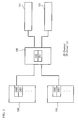
- FIG. 3 is an explanatory view of an example of use of the electronic device 100.
- the electronic device 100 is arranged between servers 150 and electronic interfaces 151 of devices such as printers or display control devices.
- the electronic device 100 converts optical signals to electrical signals and vice versa.
- an intermediate device corresponds to the electronic device 100.
- CH00 (CHANNEL 00) of the server 150 is connected to the CV0 (CONVERTER 0) of the electronic device 100 through an optical fibre, so the optical signals are transmitted and received therebetween.
- each of CV0 and CV1 is connected to the interface 151 through a cable which transmits and receives electrical signals.
- the electronic device 100 is provided with a board unit 1 within a chassis 101.
- the board unit 1 includes a printed board 2 which is an example of a board.
- the board unit 1 is provided with a back plate 3.
- the board unit 1 is inserted into the chassis 101 from the back side thereof.
- the back plate 3 is secured on the chassis 101 with screws. Also, the back plate 3 has an effect of suppressing electro magnetic interference (EMI).
- EMI electro magnetic interference
- the printed board 2 is provided with an electronic circuit.
- the electronic elements 4 are arranged at a rear end portion of the printed board 2.
- the electronic element 4 is a photoelectric conversion element which is connectable with the optical fibre cable.
- the electronic element 4 includes a connecting portion which is connectable with the optical fibre cable and which is exposed through an opening 3a.
- a printed board is provided within the electronic element 4 and is provided with a photoelectric conversion circuit which converts optical signals into electrical signals.
- a signal ground SG of the printed board is connected to an outer cover of the electronic element 4. In this way, the electronic element 4 includes the photoelectric conversion portion.
- the shield structure 110 is provided for improving the ESD resistance of the electronic element 4.
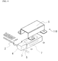
- FIG. 4 is a perspective view of the periphery of the electronic element 4.
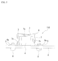
- FIG. 5 is a back view of the periphery of the electronic element 4 mounted on the printed board 2.
- the shield structure 110 includes a ground pattern 5 formed on the printed board 2, as illustrated in FIG. 4 .
- the electronic element 4 is mounted on the ground pattern 5.
- the shield structure 110 includes first hardware 6 (a first hardware component) corresponding to a first member with electrical conductivity. As illustrated in FIGs. 4 and 5 , the first hardware 6 covers the electronic element 4 and is connected with the ground pattern 5. Additionally, the first hardware 6 is detached in FIG. 4 .
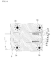
- FIG. 6 is an explanatory view of a mounting surface, on which the electronic element 4 is mounted, of the printed board 2.
- the ground pattern 5 is provided on the printed board 2 so as to cover the entire area of the mounting surface on which the electronic element 4 is mounted. However, in order to insert ground pins 4a and signal pins 4b of the electronic element 4 into via holes provided in the printed board 2, no pattern is provided at the positions corresponding to these pins.
- the ground pattern 5 acts as a signal ground.
- FIGs. 7A to 7C are third views of the first hardware 6.
- FIG. 7A is a plan view
- FIG. 7B is a front view
- FIG. 7C is a back view.
- the first hardware 6 includes: a top plate 6a; a front plate 6b; and two side plates 6c. That is, in the first hardware 6, four plates are arranged in four directions, respectively.
- the side plate 6c is provided with flange portions 6c1 extending outwardly.
- the flange portion 6c1 is provided with a screw hole 6c2.
- the first hardware 6 covers the electronic element 4 such that the flange portions 6c1 come into contact with the ground pattern 5.
- a conductive sheet 7 corresponding to a third member is arranged at the inner side of the first hardware 6.
- the conductive sheets 7 are attached on the top plate 6a and the side plates 6c so as to come into contact with the electronic element 4 when the first hardware 6 covers the electronic element 4.
- the conductive sheet 7 is applied by use of an adhesive tape having acrylic-based adhesive with electrical conductivity.
- Shield Form (product name) of ZIPPERTUBING(Japan), Ltd. is used as the conductive sheet 7.
- the conductive sheet 7 has a polyester cloth as a base with copper and nickel layers, both having conductive properties, formed thereon.
- the conductive sheet 7 is provided with a projection portion 7a.
- the projection portion 7a is formed by arranging polyurethane form within the sheet. In a case where the electronic element 4 and the first hardware 6 come into close contact with each other, the conductive sheet 7 can be eliminated. However, the provision of the conductive sheet 7 ensures a close connection between the electronic element 4 and the first hardware 6.
- the first hardware 6 covers the electronic element 4, and causes the flange portions 6c1 to come into contact with the ground pattern 5.
- screws 8 are respectively fitted into the screws holes 6c2, so that the first hardware 6 is secured.
- the first hardware 6 and the ground pattern 5 are electrically connected with each other.
- the electronic element 4 is entirely surrounded with the conductive members.
- the signal ground of the printed board arranged within the electronic element 4 is connected with the ground pattern 5 through the outer surface of the electronic element 4, the conductive sheet 7, and the first hardware 6. Consequently, the ESD resistance is improved. Therefore, the stable photoelectric conversion and signal transmission are ensured in the electronic element 4.
- the first hardware 6 and the ground pattern 5 may be connected with each other by solder instead of the screws 8.
- a connecting portion having a clip shape may be provided for connection with the ground pattern 5, and the first hardware 6 may be inserted into the connecting portion.
- the flange portion 6c1 can be eliminated. In this way, it is only necessary for the first hardware 6 to be electrically connected to the ground pattern 5.
- a shield structure 210 will be described as according to a second embodiment with reference to FIGs. 8 to 14 .
- the shield structure 110 according to the first embodiment is augmented by second hardware 20 (a second hardware component) corresponding to a second member.
- second hardware 20 a second hardware component
- the same components and configurations as those employed in the first exemplary embodiment have the same reference numerals and a detailed explanation will be omitted, if not otherwise specified.
- FIG. 8 is a perspective view of an electronic device 200 provided with the shield structure 210 according to the second embodiment.
- FIG. 9 is a back view of the electronic device 200.
- FIG. 10 is a perspective view of a board unit 2 partially cut off above the electronic element 4 in the second embodiment.
- FIG. 11 is a cross sectional view of the board unit 2 partially cut off above the electronic element 4 in the second embodiment.
- FIG. 11 is a view when viewed in the direction A illustrated in FIG. 10 .
- FIG. 12 is an exploded perspective view of the second hardware 20 included in the shield structure 210.
- FIGs. 13A to 13C are three views of parts included in the second hardware 20.
- FIG. 13A is a back view.
- FIG. 13B is a side view.
- FIG. 13C is a bottom view.
- FIGs. 14A to 14C are three views of pressing hardware 24 included in the second hardware 20.
- FIG. 14A is a plan view
- FIG. 14B is a back view
- the second hardware 20 includes: a back plate 21; a ground portion 22; a connecting portion 23; and pressing hardware 24 (pressing components), as illustrated in FIG. 12 .
- the back plate 21 corresponds to the back plate 3 in the first embodiment, as illustrated in FIG. 13 .
- the back plate 21 is provided with openings 21 a.
- the connecting portion of the electronic element 4 and the outer device (for example, the server 150 illustrated in FIG. 3 ) is exposed from the opening 21 a.
- the ground portion 22 and the connecting portion 23 are formed by bending a metallic plate.
- the metallic plate is attached to the back plate 21.
- the ground portion 22 is a portion coming into contact with the ground pattern 5 provided in the board 2.
- the connecting portion 23 is provided with a concave portion 23a having a shape corresponding to the outer shape of the first hardware 6, as illustrated in FIG. 12 .
- the connecting portion 23 is a portion which comes into contact with the first hardware 6.
- the pressing hardware 24 includes: a pressing portion 24a parallel with the top plate 6a of the first hardware 6; and two guide portions 24b parallel with the side plate 6c, as illustrated in FIGs. 14A to 14C .
- the pressing hardware 24 is attached to the connecting portion 23 with the guide portion 24b inserted into the concave portion 23a provided in the connecting portion 23, as illustrated in FIG. 12 .
- the second hardware 20 is secured on the board 2 with screws such that the ground portion 22 comes into contact with the ground pattern 5 provided on the board 2.
- a conductive sheet 25 similar to the conductive sheet 7, is arranged between the pressing portion 24a of the pressing hardware 24 and the first hardware 6, between the guide portion 24b and the first hardware 6. Accordingly, the contact property between the second hardware 20 and the first hardware 6 is improved, and the electrical connection therebetween is improved. Further, the method of securing the second hardware 20 is not limited to screws.
- the back plate 21 comes into contact with the chassis 101 as illustrated in FIG. 9 . Accordingly, the first hardware 6 corresponding to signal ground has an electric potential identical to that of frame ground through the second hardware 20. In the result, the influence of noise is reduced, and the ESD tolerance is further improved. Therefore, stable photoelectric conversion and signal transmission are ensured in the electronic element 4. Additionally, the back plate 21 has an effect of suppressing SEMI (Electro Magnetic Interference).
- SEMI Electro Magnetic Interference
- a shield structure 310 will be described as according to a third embodiment with reference to FIGs. 15 to 22 .
- the shield structure 310 according to the third embodiment in the shield structure 210 according to the second embodiment, third hardware 30 corresponding to a fourth member is added.
- the same components and configurations as those employed in the first exemplary embodiment have the same reference numerals and a detailed explanation will be omitted, if not otherwise specified.
- FIG. 15 is a perspective view of an electronic device 300 with the shield structure 310 according to the third embodiment.
- FIG. 16A is a plan view of a rear end of the electronic device 300 with the shield structure 310 according to the third embodiment.
- FIG. 16B is a back view of the electronic device 300.
- FIG. 17 is a perspective view of the board unit 2 partially cut off above the electronic element 4 according to the third embodiment.
- FIG. 18 is a cross sectional view of the board unit 2 partially cut off above the electronic element 4 according to the third embodiment.
- FIG. 18 is a view when viewed in the direction A illustrated in FIG. 17 .
- FIG. 19 is an exploded perspective view of the second hardware 20 and the third hardware 30.
- FIGs. 20A to 20C are three views of a covering hardware 31 included in the third hardware 30.
- FIG. 20A is a back view.
- FIG. 20B is a side view.
- FIG. 20C is a bottom view.
- FIGs. 21A to 21C are three views of a receiving hardware 32 included in the third hardware 30.
- FIG. 21A is a back view.
- FIG. 21B is a side view.
- FIG. 21C is a bottom view.
- FIG. 22 is an explanatory view of a distance between the back plate 21 and a distal portion of the covering hardware 31.
- the third hardware 30 includes the covering hardware 31 and the receiving hardware 32, as illustrated in FIGs. 17 to 19 .
- the receiving hardware 32 is attached to the back plate 21.
- the covering hardware 31 is attached to the receiving hardware 32.
- the covering hardware 31 includes a distal portion 31 a which is arranged apart from the openings 21 a provided in the back plate 21 included in the second hardware 20.
- the reason why the distal portion 31a is provided in this way is to deal with the low ESD tolerance occurring at a case where the covering hardware 31 comes into contact with the periphery of the opening 21 a of the back plate 21.
- the electronic element 4 is connected with an optical fibre, if a charged operator touches the periphery of the opening 21 a of the back plate 21, the electricity might be discharged. Therefore, noise caused by the electrical discharge might enter the electronic device 100, and might cause a malfunction in the electronic device 100. As illustrated in FIG.
- L is 20 mm.
- the provision of the distal portion 31 a permits the noise generated outside of the electronic device 300 to be spaced from the electronic element 4. This can improve the ESD tolerance.
- L may be set to more than or equal to 20 mm.
- the distal portion 31a is provided with openings 31a1.
- the optical fibre cable is connected to the electronic element 4 through the opening 31a1.
- the distance between the opening 31a1 and the electronic element 4 is long as illustrated in FIG. 18 .
- the electronic element 4 is arranged in the back of the covering hardware 31.
- the covering hardware 31 is attachable to and detachable from the receiving hardware 32.
- the receiving hardware 32 is provided with an attachment portion 32a attachable with the back plate 21.
- the attachment portion 32a is secured in the receiving hardware 32.
- the receiving hardware 32 is provided with a slot 32a1 at its upper portion.
- a lug portion 31b of the covering hardware 31 is inserted into the slot 32al.
- the lug portion 31b is inserted into the slot 32al, and the covering hardware 31 is secured in the receiving hardware 32 with the screws 33.
- Such a shield structure 310 according to the third embodiment is arranged within the electronic device 200 as illustrated in FIG. 15 , so the back plate 21 comes into contact with the chassis 101 as illustrated in FIG. 16B . Therefore, the first hardware 6 corresponding to the signal ground has an identical potential to that of the frame ground through the second hardware 20. This reduces the influence of the noise and improves the ESD tolerance. Also, the provision of the distal portion 31 a further improves the ESD tolerance, to be specific, in the periphery of the opening 31a1. Therefore, stable photoelectric conversion and signal transmission are ensured in the electronic element 4.
- the shield structure 410 includes fourth hardware 40 instead of the third hardware 30 of the shield structure 310 according to the third embodiment.
- the fourth hardware 40 corresponds to the fourth member.
- the same components and configurations as those employed in the first exemplary embodiment have the same reference numerals and a detailed explanation will be omitted, if not otherwise specified.
- FIG. 23 is a perspective view of an electronic device 400 with the shield structure 410 according to the third embodiment.
- FIG. 24A is a plan view of a rear end of the electronic device 400 with the shield structure 410 according to the fourth embodiment.
- FIG. 24B is a back view of the electronic device 400.
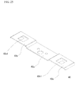
- FIG. 25 is a perspective view of the fourth hardware 40.
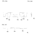
- FIGs. 26A to 26C are three views of the fourth hardware 40.
- FIG. 26A is a back view.
- FIG. 26B is a side view.
- FIG. 26C is a bottom view.
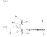
- FIG. 27 is a schematic view of a part of the shield structure 410 according to the fourth embodiment when viewed from the side thereof.
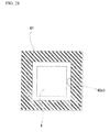
- FIG. 28 is a schematic view of the arrangement of a conductive sheet 41 in the shield structure 410 according to the fourth embodiment.
- the fourth hardware 40 includes: a contact portion 40a provided at the center; and distal portions 40b provided to extend from the contact portion 40a.
- the distal portion 40b is provided with an opening 40b1.
- the fourth hardware 40 is attached to the conductive sheet 41 such that the contact portion 40a comes into contact with the back plate 21.
- a conductive sheet 41 similar to the conductive sheet 7 is arranged between the distal portion 40b and the back plate 21 as illustrated in FIGs. 27 and 28 .
- the conductive sheet 41 is arranged, so the distance between the distal portion 40b and the back plate 21 is set to 2 mm and is smaller than the distance L between the distal portion 31 a and the back plate 21 according to the second embodiment.
- the conductive sheet 41 is arranged around the opening 40b1 as illustrated in FIG. 28 .
- the provision of the conductive sheet 41 prevents the noise from entering the device and improves the ESD tolerance. That is, the conductive sheet 41 is arranged around the opening 40b1, thereby lowering the impedance between the back plate 21 and the distal portion 40b. Accordingly, the voltage of the generated noise is lowered, thereby reducing the influence on the electronic element 4 within the electronic device 400, other electric circuits, and other electronic elements.
- the conductive sheet 41 ensures a broad contact area, thereby making the resistance low.
- the shield structure 410 including the distal portion 31a and the conductive sheet 41 can improve the ESD tolerance, in specifically, at the periphery of the opening 40b1. Consequently, stable photoelectric conversion and signal transmission are ensured in the electronic element 4.
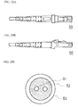
- FIGs. 29A to 29C are explanatory views of the optical fibre cable 50 attached to the electronic device.
- FIG. 29A is a plan view of a connector poriton.
- FIG. 29B is a side view of the connector portion.
- FIG. 29C is a cross sectional view of a cable.
- the optical fibre cable 50 includes: optical fibres 51 made of silicon resin and polyamide resin; a buffer layer 52 arranged around the optical fibres 51 and made of aramid fibers; and a covering 53 as the outermost layer, made of a polyvinyl chloride.
- FIG. 30 is an explanatory view of an ESD test machine 55.
- the ESD test machine 55 was provided with a discharge electrode 55a.
- the verification test was a direct discharge test in which the electricity was discharged by bringing the discharge electrode 55a into contact with a measured portion.
- the number of applications was 25 times in one second.
- a shield structure such as the first hardware 6 or the second hardware 20 was not provided and no measures for improving the ESD tolerance were taken.
- the measured ESD tolerance was about plus or minus 2 kV at each position of the chassis of the electronic device.
- the shield structure 210 of the first hardware 6 and the second hardware 20 is provided.
- the measured ESD tolerance was about plus or minus 10 kV at the positions other than the periphery of the opening 21a of the back plate 21. The improvement of the ESD tolerance was verified.
- the measured ESD tolerance was about plus or minus 2 kV in the periphery of the opening 21 a of the back plate 21.
- the shield structure 310 where the third hardware 30 is provided in addition to the second embodiment, is provided.
- the measured ESD tolerance was about plus or minus 10 kV in the periphery of the opening 31a1 of the distal portion 31 a.
- the improvement of the ESD tolerance was verified in the pheriphery of the opening.
- the shield structure 410 where the fourth hardware 40 and the conductive sheet 41 is provided in addition to the second embodient, is provided.
- the measured ESD tolerance was about plus or minus 8 kV in the periphery of the opening 40b1 of the distal portion 40b.
- the improvement of the ESD tolerance was verified in the pheriphery of the opening.
- the measured ESD tolerance was about plus or minus 6 kV in the periphery of the opening 40b1. It is considered that the conductive sheet 41 also contributes to the improvement of the ESD tolerance. Further, it is considered that the ESD tolerance is higher, as the distance between the back plate 21 and the distal portion is longer in light of the comparison with the third embodiment.
- the shield structures described herein improve the ESD tolerance by providing the signal ground and the frame ground for the interface of the electronic device.
Landscapes
- Engineering & Computer Science (AREA)
- Theoretical Computer Science (AREA)
- Computer Hardware Design (AREA)
- General Engineering & Computer Science (AREA)
- Microelectronics & Electronic Packaging (AREA)
- Power Engineering (AREA)
- Human Computer Interaction (AREA)
- Physics & Mathematics (AREA)
- General Physics & Mathematics (AREA)
- Shielding Devices Or Components To Electric Or Magnetic Fields (AREA)
Abstract
Description
- The present invention relates to a shield structure and an electronic device.
- It is important to suppress noise in an electronic device. Various noise suppression techniques of an electronic device have been proposed. For example, there is proposed a shield member separately shielding a subject circuit portion and a signal input and output portion in Japanese Examined Patent Application Publication No.
7-96009 3516407 - In a case where an electronic device employs an electronic element, particularly, one having sensitivity to noise, static electricity generated outside the electronic device might cause a malfunction an electronic circuit or an electronic element in the electronic device. For example, in a photoelectric conversion element that includes a photoelectric conversion portion converting optical signals into electrical signals, the photoelectric conversion element is affected by noise and has low electrostatic discharge (ESD) resistance.
- In light of these problems, the proposals of the above mentioned patent documents shield the entire board or a special area. The improvement in the ESD resistance of the electronic element is insufficient.
- Accordingly, it is desirable to provide a shield structure and an electronic device for improving the ESD resistance of an electronic element.
- According to an aspect of the embodiments, a shield structure for an electronic element includes: a ground pattern provided in a board; and a first member having electrical conductivity, covering the electronic element, and connected with the ground pattern.
- The advantages of the invention will be realized and attained by means of the elements and combinations particularly pointed out in the claims.
- It is to be understood that both the foregoing general description and the following detailed description are exemplary and explanatory and are not restrictive of the invention, as claimed.
- Reference is made, by way of example only, to the accompanying drawings in which:
-
FIG. 1 is a perspective view of an electronic device with a shield structure according to a first embodiment; -
FIG. 2 is a back view of the electronic device with the shield structure according to the first embodiment; -
FIG. 3 is an explanatory view of an example of use of the electronic device according to the first embodiment; -
FIG. 4 is a perspective view of the periphery of an electronic element with a first hardware being removed according to the first embodiment; -
FIG. 5 is a back view of the periphery of the electronic element according to the first embodiment; -
FIG. 6 is an explanatory view of a surface, on which the electronic element is mounted, of a board according to the first embodiment; -
FIGs. 7A to 7C are three views of a first hardware,FIG. 7A is a plan view,FIG. 7B is a side view, andFIG. 7C is a back view; -
FIG. 8 is a perspective view of an electronic element with a shield structure according to a second embodiment; -
FIG. 9 is a back view of the electronic device with the shield structure according to the second embodiment; -
FIG. 10 is a perspective view of a board unit partially cut off above the electronic element according to the second embodiment; -
FIG. 11 is a cross sectional view of a board unit partially cut off above the electronic element according to the second embodiment; -
FIG. 12 is an exploded perspective view of a second hardware; -
FIGs. 13A to 13C are three views of hardware included in the second hardware,FIG. 13A is a back view,FIG. 13B is a side view, andFIG. 13C is a bottom view; -
FIGs. 14A to 14C are three views of pressing hardware included in the second hardware,FIG. 14A is a plan view,FIG. 14B is a back view, andFIG. 14C is a side view; -
FIG. 15 is a perspective view of an electronic device with a shield structure according to the third embodiment; -
FIG. 16A is a plan view of a rear end of the electronic device with the shield structure according to the third embodiment, andFIG. 16B is a back view of the electronic device; -
FIG. 17 is a perspective view of the board unit partially cut off above the electronic element according to the third embodiment; -
FIG. 18 is a cross sectional view of the board unit partially cut off above the electronic element according to the third embodiment; -
FIG. 19 is an exploded perspective view of the second hardware and a third hardware; -
FIGs. 20A to 20C are three views of a covering hardware included in the third hardware,FIG. 20A is a back view,FIG. 20B is a side view, andFIG. 20C is a bottom view; -
FIGs. 21A to 21C are three views of a receiving hardware included in the third hardware,FIG. 21A is a back view,FIG. 21B is a side view, andFIG. 21C is a bottom view; -
FIG. 22 is an explanatory view of a distance between a back plate and a distal portion of the covering hardware; -
FIG. 23 is a perspective view of an electronic device with a shield structure according to the third embodiment; -
FIG. 24A is a plan view of a rear end of the electronic device with the shield structure according to the fourth embodiment, andFIG. 24B is a back view of the electronic device; -
FIG. 25 is a perspective view of the fourth hardware; -
FIGs. 26A to 26C are three views of the fourth hardware,FIG. 26A is a back view,FIG. 26B is a side view, andFIG. 26C is a bottom view; -
FIG. 27 is a schematic view of a part of the shield structure according to the fourth embodiment when viewed from the side thereof; -
FIG. 28 is a schematic view of the arrangement of a conductive sheet in the shield structure according to the fourth embodiment; -
FIGs. 29A to 29C are explanatory views of an optical fibre cable attached to the electronic device; and -
FIG. 30 is an explanatory view of an ESD test machine. - In the following, embodiments will be described with reference to the accompanying drawings. However, dimensions and ratios of components may be identified to those of real components (shown not to scale). Further, details may be omitted in drawings.
-
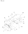
FIG. 1 is a perspective view of anelectronic device 100 with ashield structure 110 according to a first embodiment.FIG. 2 is a back view of theelectronic device 100 with theshield structure 110 according to the first embodiment.FIG. 3 is an explanatory view of an example of use of theelectronic device 100. Theelectronic device 100 is arranged betweenservers 150 andelectronic interfaces 151 of devices such as printers or display control devices. Theelectronic device 100 converts optical signals to electrical signals and vice versa. InFIG. 3 , an intermediate device corresponds to theelectronic device 100. In the example as illustrated inFIG. 3 , CH00 (CHANNEL 00) of theserver 150 is connected to the CV0 (CONVERTER 0) of theelectronic device 100 through an optical fibre, so the optical signals are transmitted and received therebetween. Further, each of CV0 and CV1 is connected to theinterface 151 through a cable which transmits and receives electrical signals. - The
electronic device 100 is provided with aboard unit 1 within achassis 101. Theboard unit 1 includes a printedboard 2 which is an example of a board. Theboard unit 1 is provided with aback plate 3. Theboard unit 1 is inserted into thechassis 101 from the back side thereof. Theback plate 3 is secured on thechassis 101 with screws. Also, theback plate 3 has an effect of suppressing electro magnetic interference (EMI). - The printed
board 2 is provided with an electronic circuit. Theelectronic elements 4 are arranged at a rear end portion of the printedboard 2. Theelectronic element 4 is a photoelectric conversion element which is connectable with the optical fibre cable. Theelectronic element 4 includes a connecting portion which is connectable with the optical fibre cable and which is exposed through anopening 3a. A printed board is provided within theelectronic element 4 and is provided with a photoelectric conversion circuit which converts optical signals into electrical signals. A signal ground SG of the printed board is connected to an outer cover of theelectronic element 4. In this way, theelectronic element 4 includes the photoelectric conversion portion. Theshield structure 110 is provided for improving the ESD resistance of theelectronic element 4. -
FIG. 4 is a perspective view of the periphery of theelectronic element 4.FIG. 5 is a back view of the periphery of theelectronic element 4 mounted on the printedboard 2. - The
shield structure 110 includes aground pattern 5 formed on the printedboard 2, as illustrated inFIG. 4 . Theelectronic element 4 is mounted on theground pattern 5. Theshield structure 110 includes first hardware 6 (a first hardware component) corresponding to a first member with electrical conductivity. As illustrated inFIGs. 4 and5 , thefirst hardware 6 covers theelectronic element 4 and is connected with theground pattern 5. Additionally, thefirst hardware 6 is detached inFIG. 4 . -
FIG. 6 is an explanatory view of a mounting surface, on which theelectronic element 4 is mounted, of the printedboard 2. Theground pattern 5 is provided on the printedboard 2 so as to cover the entire area of the mounting surface on which theelectronic element 4 is mounted. However, in order to insert ground pins 4a andsignal pins 4b of theelectronic element 4 into via holes provided in the printedboard 2, no pattern is provided at the positions corresponding to these pins. Theground pattern 5 acts as a signal ground. -
FIGs. 7A to 7C are third views of thefirst hardware 6.FIG. 7A is a plan view,FIG. 7B is a front view, andFIG. 7C is a back view. Thefirst hardware 6 includes: atop plate 6a; afront plate 6b; and twoside plates 6c. That is, in thefirst hardware 6, four plates are arranged in four directions, respectively. Theside plate 6c is provided with flange portions 6c1 extending outwardly. The flange portion 6c1 is provided with a screw hole 6c2. - The
first hardware 6 covers theelectronic element 4 such that the flange portions 6c1 come into contact with theground pattern 5. In this case, aconductive sheet 7 corresponding to a third member is arranged at the inner side of thefirst hardware 6. Theconductive sheets 7 are attached on thetop plate 6a and theside plates 6c so as to come into contact with theelectronic element 4 when thefirst hardware 6 covers theelectronic element 4. Theconductive sheet 7 is applied by use of an adhesive tape having acrylic-based adhesive with electrical conductivity. In the present embodiment, Shield Form (product name) of ZIPPERTUBING(Japan), Ltd., is used as theconductive sheet 7. - The
conductive sheet 7 has a polyester cloth as a base with copper and nickel layers, both having conductive properties, formed thereon. Theconductive sheet 7 is provided with aprojection portion 7a. Theprojection portion 7a is formed by arranging polyurethane form within the sheet. In a case where theelectronic element 4 and thefirst hardware 6 come into close contact with each other, theconductive sheet 7 can be eliminated. However, the provision of theconductive sheet 7 ensures a close connection between theelectronic element 4 and thefirst hardware 6. - The
first hardware 6 covers theelectronic element 4, and causes the flange portions 6c1 to come into contact with theground pattern 5. Next, screws 8 are respectively fitted into the screws holes 6c2, so that thefirst hardware 6 is secured. Accordingly, thefirst hardware 6 and theground pattern 5 are electrically connected with each other. In the result, theelectronic element 4 is entirely surrounded with the conductive members. Further, the signal ground of the printed board arranged within theelectronic element 4 is connected with theground pattern 5 through the outer surface of theelectronic element 4, theconductive sheet 7, and thefirst hardware 6. Consequently, the ESD resistance is improved. Therefore, the stable photoelectric conversion and signal transmission are ensured in theelectronic element 4. Additionally, thefirst hardware 6 and theground pattern 5 may be connected with each other by solder instead of thescrews 8. Further, a connecting portion having a clip shape may be provided for connection with theground pattern 5, and thefirst hardware 6 may be inserted into the connecting portion. In this case, the flange portion 6c1 can be eliminated. In this way, it is only necessary for thefirst hardware 6 to be electrically connected to theground pattern 5. - Next, a
shield structure 210 will be described as according to a second embodiment with reference toFIGs. 8 to 14 . In theshield structure 210 according to the second embodiment, theshield structure 110 according to the first embodiment is augmented by second hardware 20 (a second hardware component) corresponding to a second member. Hereinafter, in the second exemplary embodiment, the same components and configurations as those employed in the first exemplary embodiment have the same reference numerals and a detailed explanation will be omitted, if not otherwise specified. -
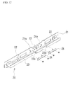
FIG. 8 is a perspective view of anelectronic device 200 provided with theshield structure 210 according to the second embodiment.FIG. 9 is a back view of theelectronic device 200.FIG. 10 is a perspective view of aboard unit 2 partially cut off above theelectronic element 4 in the second embodiment.FIG. 11 is a cross sectional view of theboard unit 2 partially cut off above theelectronic element 4 in the second embodiment.FIG. 11 is a view when viewed in the direction A illustrated inFIG. 10 .FIG. 12 is an exploded perspective view of thesecond hardware 20 included in theshield structure 210.FIGs. 13A to 13C are three views of parts included in thesecond hardware 20.FIG. 13A is a back view.FIG. 13B is a side view.FIG. 13C is a bottom view.FIGs. 14A to 14C are three views of pressinghardware 24 included in thesecond hardware 20.FIG. 14A is a plan view,FIG. 14B is a back view, andFIG. 14C is a side view. - The
second hardware 20 includes: aback plate 21; aground portion 22; a connectingportion 23; and pressing hardware 24 (pressing components), as illustrated inFIG. 12 . Theback plate 21 corresponds to theback plate 3 in the first embodiment, as illustrated inFIG. 13 . Theback plate 21 is provided withopenings 21 a. The connecting portion of theelectronic element 4 and the outer device (for example, theserver 150 illustrated inFIG. 3 ) is exposed from the opening 21 a. Theground portion 22 and the connectingportion 23 are formed by bending a metallic plate. The metallic plate is attached to theback plate 21. Theground portion 22 is a portion coming into contact with theground pattern 5 provided in theboard 2. Further, the connectingportion 23 is provided with aconcave portion 23a having a shape corresponding to the outer shape of thefirst hardware 6, as illustrated inFIG. 12 . The connectingportion 23 is a portion which comes into contact with thefirst hardware 6. Thepressing hardware 24 includes: apressing portion 24a parallel with thetop plate 6a of thefirst hardware 6; and twoguide portions 24b parallel with theside plate 6c, as illustrated inFIGs. 14A to 14C . Thepressing hardware 24 is attached to the connectingportion 23 with theguide portion 24b inserted into theconcave portion 23a provided in the connectingportion 23, as illustrated inFIG. 12 . - As illustrated in
FIGs. 10 and11 , thesecond hardware 20 is secured on theboard 2 with screws such that theground portion 22 comes into contact with theground pattern 5 provided on theboard 2. In this case, aconductive sheet 25, similar to theconductive sheet 7, is arranged between thepressing portion 24a of thepressing hardware 24 and thefirst hardware 6, between theguide portion 24b and thefirst hardware 6. Accordingly, the contact property between thesecond hardware 20 and thefirst hardware 6 is improved, and the electrical connection therebetween is improved. Further, the method of securing thesecond hardware 20 is not limited to screws. - In the
shield structure 210 according to the second embodiment, when theboard unit 1 is arranged within theelectronic device 200 as illustrated inFIG. 8 , theback plate 21 comes into contact with thechassis 101 as illustrated inFIG. 9 . Accordingly, thefirst hardware 6 corresponding to signal ground has an electric potential identical to that of frame ground through thesecond hardware 20. In the result, the influence of noise is reduced, and the ESD tolerance is further improved. Therefore, stable photoelectric conversion and signal transmission are ensured in theelectronic element 4. Additionally, theback plate 21 has an effect of suppressing SEMI (Electro Magnetic Interference). - Next, a
shield structure 310 will be described as according to a third embodiment with reference toFIGs. 15 to 22 . In theshield structure 310 according to the third embodiment, in theshield structure 210 according to the second embodiment,third hardware 30 corresponding to a fourth member is added. Hereinafter, in the second exemplary embodiment, the same components and configurations as those employed in the first exemplary embodiment have the same reference numerals and a detailed explanation will be omitted, if not otherwise specified. -
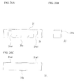
FIG. 15 is a perspective view of anelectronic device 300 with theshield structure 310 according to the third embodiment.FIG. 16A is a plan view of a rear end of theelectronic device 300 with theshield structure 310 according to the third embodiment.FIG. 16B is a back view of theelectronic device 300.FIG. 17 is a perspective view of theboard unit 2 partially cut off above theelectronic element 4 according to the third embodiment.FIG. 18 is a cross sectional view of theboard unit 2 partially cut off above theelectronic element 4 according to the third embodiment.FIG. 18 is a view when viewed in the direction A illustrated inFIG. 17 .FIG. 19 is an exploded perspective view of thesecond hardware 20 and thethird hardware 30.FIGs. 20A to 20C are three views of a coveringhardware 31 included in thethird hardware 30.FIG. 20A is a back view.FIG. 20B is a side view.FIG. 20C is a bottom view.FIGs. 21A to 21C are three views of a receivinghardware 32 included in thethird hardware 30.FIG. 21A is a back view.FIG. 21B is a side view.FIG. 21C is a bottom view.FIG. 22 is an explanatory view of a distance between theback plate 21 and a distal portion of the coveringhardware 31. - The
third hardware 30 includes the coveringhardware 31 and the receivinghardware 32, as illustrated inFIGs. 17 to 19 . The receivinghardware 32 is attached to theback plate 21. The coveringhardware 31 is attached to the receivinghardware 32. - The covering
hardware 31 includes adistal portion 31 a which is arranged apart from theopenings 21 a provided in theback plate 21 included in thesecond hardware 20. The reason why thedistal portion 31a is provided in this way is to deal with the low ESD tolerance occurring at a case where the coveringhardware 31 comes into contact with the periphery of the opening 21 a of theback plate 21. Specifically, after theelectronic element 4 is connected with an optical fibre, if a charged operator touches the periphery of the opening 21 a of theback plate 21, the electricity might be discharged. Therefore, noise caused by the electrical discharge might enter theelectronic device 100, and might cause a malfunction in theelectronic device 100. As illustrated inFIG. 22 , thedistal portion 31 a and theback plate 21 included in thesecond hardware 20 are spaced by the distance L. In the illustrated coveringhardware 31, L is 20 mm. The provision of thedistal portion 31 a permits the noise generated outside of theelectronic device 300 to be spaced from theelectronic element 4. This can improve the ESD tolerance. L may be set to more than or equal to 20 mm. - The
distal portion 31a is provided with openings 31a1. The optical fibre cable is connected to theelectronic element 4 through the opening 31a1. However, the distance between the opening 31a1 and theelectronic element 4 is long as illustrated inFIG. 18 . In other words, theelectronic element 4 is arranged in the back of the coveringhardware 31. For this reason, it is difficult for the optical fibre cable to be connected to and disconnected from theelectronic element 4. Accordingly, the coveringhardware 31 is attachable to and detachable from the receivinghardware 32. The receivinghardware 32 is provided with anattachment portion 32a attachable with theback plate 21. Theattachment portion 32a is secured in the receivinghardware 32. The receivinghardware 32 is provided with a slot 32a1 at its upper portion. Alug portion 31b of the coveringhardware 31 is inserted into the slot 32al. Thelug portion 31b is inserted into the slot 32al, and the coveringhardware 31 is secured in the receivinghardware 32 with thescrews 33. - Such a
shield structure 310 according to the third embodiment is arranged within theelectronic device 200 as illustrated inFIG. 15 , so theback plate 21 comes into contact with thechassis 101 as illustrated inFIG. 16B . Therefore, thefirst hardware 6 corresponding to the signal ground has an identical potential to that of the frame ground through thesecond hardware 20. This reduces the influence of the noise and improves the ESD tolerance. Also, the provision of thedistal portion 31 a further improves the ESD tolerance, to be specific, in the periphery of the opening 31a1. Therefore, stable photoelectric conversion and signal transmission are ensured in theelectronic element 4. - Next, a
shield structure 410 will be described as according to a fourth embodiment with reference toFIGs. 23 to 28 . Theshield structure 410 according to the fourth embodiment includesfourth hardware 40 instead of thethird hardware 30 of theshield structure 310 according to the third embodiment. Thefourth hardware 40 corresponds to the fourth member. Hereinafter, in the second exemplary embodiment, the same components and configurations as those employed in the first exemplary embodiment have the same reference numerals and a detailed explanation will be omitted, if not otherwise specified. -
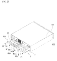
FIG. 23 is a perspective view of anelectronic device 400 with theshield structure 410 according to the third embodiment.FIG. 24A is a plan view of a rear end of theelectronic device 400 with theshield structure 410 according to the fourth embodiment.FIG. 24B is a back view of theelectronic device 400.FIG. 25 is a perspective view of thefourth hardware 40.FIGs. 26A to 26C are three views of thefourth hardware 40.FIG. 26A is a back view.FIG. 26B is a side view.FIG. 26C is a bottom view.FIG. 27 is a schematic view of a part of theshield structure 410 according to the fourth embodiment when viewed from the side thereof.FIG. 28 is a schematic view of the arrangement of aconductive sheet 41 in theshield structure 410 according to the fourth embodiment. - As illustrated in
FIGs. 25 to 26C , thefourth hardware 40 includes: acontact portion 40a provided at the center; anddistal portions 40b provided to extend from thecontact portion 40a. Thedistal portion 40b is provided with an opening 40b1. - The
fourth hardware 40 is attached to theconductive sheet 41 such that thecontact portion 40a comes into contact with theback plate 21. Aconductive sheet 41 similar to theconductive sheet 7 is arranged between thedistal portion 40b and theback plate 21 as illustrated inFIGs. 27 and28 . Theconductive sheet 41 is arranged, so the distance between thedistal portion 40b and theback plate 21 is set to 2 mm and is smaller than the distance L between thedistal portion 31 a and theback plate 21 according to the second embodiment. Theconductive sheet 41 is arranged around the opening 40b1 as illustrated inFIG. 28 . - In this way, the provision of the
conductive sheet 41 prevents the noise from entering the device and improves the ESD tolerance. That is, theconductive sheet 41 is arranged around the opening 40b1, thereby lowering the impedance between theback plate 21 and thedistal portion 40b. Accordingly, the voltage of the generated noise is lowered, thereby reducing the influence on theelectronic element 4 within theelectronic device 400, other electric circuits, and other electronic elements. Theconductive sheet 41 ensures a broad contact area, thereby making the resistance low. - The
shield structure 410, according to the fourth embodiment, including thedistal portion 31a and theconductive sheet 41 can improve the ESD tolerance, in specifically, at the periphery of the opening 40b1. Consequently, stable photoelectric conversion and signal transmission are ensured in theelectronic element 4. - Next, a description will be given of a verification test of the shield structure mentioned above. Here, the description will be given of the shield structures according to the second, third, and fourth embodiments in which the frame ground connection is ensured. When the verification test was performed, an
optical fibre cable 50 was attached to theelectronic element 4 in order to realize its actual use state. In the test, theoptical fibre cable 50 made by Furukawa Electric Co., Ltd. was used.FIGs. 29A to 29C are explanatory views of theoptical fibre cable 50 attached to the electronic device.FIG. 29A is a plan view of a connector poriton.FIG. 29B is a side view of the connector portion.FIG. 29C is a cross sectional view of a cable. Theoptical fibre cable 50 includes:optical fibres 51 made of silicon resin and polyamide resin; abuffer layer 52 arranged around theoptical fibres 51 and made of aramid fibers; and a covering 53 as the outermost layer, made of a polyvinyl chloride. -
FIG. 30 is an explanatory view of anESD test machine 55. TheESD test machine 55 was provided with adischarge electrode 55a. The verification test was a direct discharge test in which the electricity was discharged by bringing thedischarge electrode 55a into contact with a measured portion. The number of applications was 25 times in one second. - In this case, a shield structure such as the
first hardware 6 or thesecond hardware 20 was not provided and no measures for improving the ESD tolerance were taken. - The measured ESD tolerance was about plus or minus 2 kV at each position of the chassis of the electronic device.
- In this case, the
shield structure 210 of thefirst hardware 6 and thesecond hardware 20 is provided. In this case, the measured ESD tolerance was about plus or minus 10 kV at the positions other than the periphery of theopening 21a of theback plate 21. The improvement of the ESD tolerance was verified. - However, the measured ESD tolerance was about plus or minus 2 kV in the periphery of the opening 21 a of the
back plate 21. - In this case, the
shield structure 310, where thethird hardware 30 is provided in addition to the second embodiment, is provided. In this case, the measured ESD tolerance was about plus or minus 10 kV in the periphery of the opening 31a1 of thedistal portion 31 a. The improvement of the ESD tolerance was verified in the pheriphery of the opening. - In this case, the
shield structure 410, where thefourth hardware 40 and theconductive sheet 41 is provided in addition to the second embodient, is provided. In this case, the measured ESD tolerance was about plus or minus 8 kV in the periphery of the opening 40b1 of thedistal portion 40b. The improvement of the ESD tolerance was verified in the pheriphery of the opening. Additionally, when theconductive sheet 41 is removed, the measured ESD tolerance was about plus or minus 6 kV in the periphery of the opening 40b1. It is considered that theconductive sheet 41 also contributes to the improvement of the ESD tolerance. Further, it is considered that the ESD tolerance is higher, as the distance between theback plate 21 and the distal portion is longer in light of the comparison with the third embodiment. - The shield structures described herein improve the ESD tolerance by providing the signal ground and the frame ground for the interface of the electronic device.
- All examples and conditional language recited herein are intended for pedagogical purposes to aid the reader in understanding the invention and the concepts contributed by the inventor to furthering the art, and are to be constructed as being without limitation to such specifically recited examples and conditions, nor does the organization of such examples in the specification relate to a showing of the superiority and inferiority of the invention. Although the embodiment of the present inventions has been described in detail, it should be understood that the various changes, substitutions, and alterations could be made hereto without departing from the scope of the claims.
Claims (7)
- A shield structure for an electronic element, comprising:a ground pattern provided in a board; anda first member having electrical conductivity, arranged to cover the electronic element, and connected with the ground pattern.
- The shield structure for an electronic element of claim 1, further comprising a second member having electrical conductivity, arranged to come into contact with a chassis of an electronic device including the electronic element, and to come into contact with the ground pattern and the first member.
- The shield structure for an electronic element of claim 2, further comprising a third member having electrical conductivity, arranged at an inside of the first member, and arranged to come into contact with the electronic element.
- The shield structure for an electronic element of claim 2, further comprising a fourth member including a distal portion spaced apart from an opening, of the second member, for connecting the electronic element with an external device.
- The shield structure for an electronic element of claim 4, further comprising a fifth member having electrical conductivity, and arranged between the second and fourth members.
- An electronic device comprising the shield structure for an electronic element of any one of claims 1 to 5.
- The electronic device of claim 6, wherein the electronic element is a photoelectric conversion element.
Applications Claiming Priority (1)
| Application Number | Priority Date | Filing Date | Title |
|---|---|---|---|
| JP2010019361A JP5593714B2 (en) | 2010-01-29 | 2010-01-29 | Electronic element shield structure and electronic device equipped with the same |
Publications (2)
| Publication Number | Publication Date |
|---|---|
| EP2355644A2 true EP2355644A2 (en) | 2011-08-10 |
| EP2355644A3 EP2355644A3 (en) | 2011-10-05 |
Family
ID=44041562
Family Applications (1)
| Application Number | Title | Priority Date | Filing Date |
|---|---|---|---|
| EP11152031A Withdrawn EP2355644A3 (en) | 2010-01-29 | 2011-01-25 | Shield structure for an electronic element and electronic device |
Country Status (4)
| Country | Link |
|---|---|
| US (1) | US8797763B2 (en) |
| EP (1) | EP2355644A3 (en) |
| JP (1) | JP5593714B2 (en) |
| KR (1) | KR101191468B1 (en) |
Cited By (1)
| Publication number | Priority date | Publication date | Assignee | Title |
|---|---|---|---|---|
| CN106664815A (en) * | 2014-08-01 | 2017-05-10 | 华为技术有限公司 | Electromagnetic shielding material and method for packaging optical module |
Families Citing this family (5)
| Publication number | Priority date | Publication date | Assignee | Title |
|---|---|---|---|---|
| US8724343B2 (en) * | 2011-06-27 | 2014-05-13 | Crestron Electronics Inc. | Hi-definition multimedia interface shield with fingers |
| US20140297000A1 (en) * | 2011-11-30 | 2014-10-02 | Mitsubishi Electric Corporation | Control system, control device, connecting line, and drive device |
| US11457524B2 (en) * | 2019-04-29 | 2022-09-27 | Nxp B.V. | Integrated filter for de-sense reduction |
| US11102894B2 (en) * | 2020-01-10 | 2021-08-24 | The Boeing Company | Saddle type electrical enclosure |
| JP2026028671A (en) * | 2024-08-07 | 2026-02-20 | Astemo株式会社 | Electronic control unit |
Citations (2)
| Publication number | Priority date | Publication date | Assignee | Title |
|---|---|---|---|---|
| JPH0796009B2 (en) | 1989-01-23 | 1995-10-18 | オリンパス光学工業株式会社 | Shield device for endoscopic imaging device |
| JP3516407B2 (en) | 1994-04-08 | 2004-04-05 | 株式会社東芝 | Data transmission apparatus and X-ray CT apparatus using the same |
Family Cites Families (29)
| Publication number | Priority date | Publication date | Assignee | Title |
|---|---|---|---|---|
| JPH0397997A (en) | 1989-09-08 | 1991-04-23 | Oji Paper Co Ltd | Manufacturing method of coated paper for gravure printing |
| JPH0397997U (en) * | 1990-01-25 | 1991-10-09 | ||
| JPH052482A (en) | 1991-06-24 | 1993-01-08 | Fujitsu Ltd | Data processing device |
| JPH06283234A (en) * | 1993-03-29 | 1994-10-07 | Nec Eng Ltd | Internally storing method of external interface connector and cover structure |
| JPH0796009A (en) | 1993-09-30 | 1995-04-11 | Suzuki Motor Corp | Electric tricycle |
| KR0169840B1 (en) * | 1995-11-14 | 1999-04-15 | 양승택 | Printed Circuit Board Guide Rail System with Anti-Static Function |
| US5696669A (en) | 1996-01-11 | 1997-12-09 | Molex Incorporated | Shielding system for PC cards |
| US5717577A (en) * | 1996-10-30 | 1998-02-10 | Ericsson, Inc. | Gasketed shield can for shielding emissions of electromagnetic energy |
| US5763900A (en) * | 1996-12-05 | 1998-06-09 | Taiwan Liton Electronic Co. Ltd. | Infrared transceiver package |
| US6049469A (en) * | 1997-08-20 | 2000-04-11 | Dell Usa, L.P. | Combination electromagnetic shield and heat spreader |
| JP2000340305A (en) * | 1999-05-25 | 2000-12-08 | Seiko Epson Corp | External interface connector grounding structure |
| US6624432B1 (en) | 1999-10-12 | 2003-09-23 | Shielding For Electronics, Inc. | EMI containment apparatus |
| US6320122B1 (en) * | 1999-10-12 | 2001-11-20 | Hewlett Packard Company | Electromagnetic interference gasket |
| JP3315969B2 (en) * | 2000-05-09 | 2002-08-19 | 株式会社ソニー・コンピュータエンタテインメント | Electronics |
| NL1016549C2 (en) | 2000-10-06 | 2002-04-10 | Stork Screens Bv | Method for the production of a card protected against interference radiation with a printed circuit. |
| JP2003017193A (en) | 2001-07-04 | 2003-01-17 | Nec Tokin Iwate Ltd | Shield connector |
| US6443768B1 (en) * | 2001-09-14 | 2002-09-03 | Molex Incorporated | Small form factor connector cage |
| KR100896405B1 (en) * | 2001-12-14 | 2009-05-08 | 레어드 테크놀로지스 인코포레이티드 | EMI shielding with lossy media |
| JP4632289B2 (en) | 2002-03-06 | 2011-02-16 | タイコ・エレクトロニクス・コーポレイション | Pluggable electronic module and heat sink receptacle |
| US6744640B2 (en) * | 2002-04-10 | 2004-06-01 | Gore Enterprise Holdings, Inc. | Board-level EMI shield with enhanced thermal dissipation |
| WO2004077898A2 (en) * | 2003-02-26 | 2004-09-10 | Wavezero Inc. | Methods and devices for connecting and grounding an emi shield to a printed circuit board |
| CN1833341B (en) * | 2003-03-31 | 2010-06-16 | 莫莱克斯公司 | Shielded Cans with Improved EMI Shielding Gasket Construction |
| JP4299152B2 (en) * | 2004-01-08 | 2009-07-22 | 日本碍子株式会社 | Electromagnetic wave shielding case and manufacturing method thereof |
| JP2006090471A (en) | 2004-09-24 | 2006-04-06 | Fuji Heavy Ind Ltd | Orthogonal gear pair design device |
| WO2006090471A1 (en) | 2005-02-25 | 2006-08-31 | Fujitsu Limited | Plug-in unit and communication device |
| JP4703454B2 (en) * | 2006-03-27 | 2011-06-15 | 富士通株式会社 | Cage mounting structure for optical modules |
| CN101094584A (en) | 2006-06-21 | 2007-12-26 | 华硕电脑股份有限公司 | Shielding Modules for Electronic Components |
| CN101600331B (en) * | 2008-06-04 | 2012-10-03 | 富士康(昆山)电脑接插件有限公司 | Shield |
| JP2010192759A (en) * | 2009-02-19 | 2010-09-02 | Sanyo Electric Co Ltd | Electromagnetic shield structure of electronic apparatus housing |
-
2010
- 2010-01-29 JP JP2010019361A patent/JP5593714B2/en not_active Expired - Fee Related
-
2011
- 2011-01-13 US US13/005,718 patent/US8797763B2/en not_active Expired - Fee Related
- 2011-01-25 EP EP11152031A patent/EP2355644A3/en not_active Withdrawn
- 2011-01-27 KR KR1020110008347A patent/KR101191468B1/en not_active Expired - Fee Related
Patent Citations (2)
| Publication number | Priority date | Publication date | Assignee | Title |
|---|---|---|---|---|
| JPH0796009B2 (en) | 1989-01-23 | 1995-10-18 | オリンパス光学工業株式会社 | Shield device for endoscopic imaging device |
| JP3516407B2 (en) | 1994-04-08 | 2004-04-05 | 株式会社東芝 | Data transmission apparatus and X-ray CT apparatus using the same |
Cited By (3)
| Publication number | Priority date | Publication date | Assignee | Title |
|---|---|---|---|---|
| CN106664815A (en) * | 2014-08-01 | 2017-05-10 | 华为技术有限公司 | Electromagnetic shielding material and method for packaging optical module |
| EP3163995A4 (en) * | 2014-08-01 | 2017-11-08 | Huawei Technologies Co. Ltd. | Electromagnetic shielding material and method for packaging optical module |
| US10178817B2 (en) | 2014-08-01 | 2019-01-08 | Huawei Technologies Co., Ltd | Electromagnetic shielding material and method for packaging optical module |
Also Published As
| Publication number | Publication date |
|---|---|
| US20110188227A1 (en) | 2011-08-04 |
| JP2011159741A (en) | 2011-08-18 |
| US8797763B2 (en) | 2014-08-05 |
| JP5593714B2 (en) | 2014-09-24 |
| KR101191468B1 (en) | 2012-10-15 |
| KR20110089080A (en) | 2011-08-04 |
| EP2355644A3 (en) | 2011-10-05 |
Similar Documents
| Publication | Publication Date | Title |
|---|---|---|
| US11011874B2 (en) | Connector and connector assembly | |
| EP2355644A2 (en) | Shield structure for an electronic element and electronic device | |
| US7612299B2 (en) | Shield assembly with gaskets | |
| JP6434656B2 (en) | Electronic equipment | |
| EP3683650B1 (en) | Display screen assembly and mobile terminal | |
| JP2011114077A (en) | Electronic device | |
| CN113396511A (en) | Shell-less electric connector and its making method | |
| JP6453758B2 (en) | Electrical equipment | |
| KR102808943B1 (en) | Electronic device including interposer | |
| CN102687349B (en) | Sheet metal structures and electronic devices | |
| KR101993374B1 (en) | Connecting device for electronic components of portable terminal | |
| JPWO2004093036A1 (en) | Thin display device and plasma display | |
| JP2020031050A (en) | Cable device | |
| US8525046B2 (en) | Electronic apparatus | |
| CN104640389B (en) | Cable backplane system with stiffeners | |
| KR102651042B1 (en) | Cable device | |
| US8319879B2 (en) | Electronic apparatus | |
| CN115426769B (en) | Flexible circuit board, display module and display device | |
| EP2239779B1 (en) | Flexible image-sensing module with anti-EMI function | |
| JP4325177B2 (en) | Optical transmission module | |
| CN212084543U (en) | Display device of vehicle-mounted multimedia host | |
| KR20200043228A (en) | Cable device | |
| JP2011199023A (en) | Substrate assembly and electronic equipment including the same | |
| JP5257326B2 (en) | Portable terminal | |
| JP4141852B2 (en) | Electronic circuit unit |
Legal Events
| Date | Code | Title | Description |
|---|---|---|---|
| PUAI | Public reference made under article 153(3) epc to a published international application that has entered the european phase |
Free format text: ORIGINAL CODE: 0009012 |
|
| AK | Designated contracting states |
Kind code of ref document: A2 Designated state(s): AL AT BE BG CH CY CZ DE DK EE ES FI FR GB GR HR HU IE IS IT LI LT LU LV MC MK MT NL NO PL PT RO RS SE SI SK SM TR |
|
| AX | Request for extension of the european patent |
Extension state: BA ME |
|
| PUAL | Search report despatched |
Free format text: ORIGINAL CODE: 0009013 |
|
| AK | Designated contracting states |
Kind code of ref document: A3 Designated state(s): AL AT BE BG CH CY CZ DE DK EE ES FI FR GB GR HR HU IE IS IT LI LT LU LV MC MK MT NL NO PL PT RO RS SE SI SK SM TR |
|
| AX | Request for extension of the european patent |
Extension state: BA ME |
|
| RIC1 | Information provided on ipc code assigned before grant |
Ipc: G06F 1/18 20060101ALI20110829BHEP Ipc: H05K 9/00 20060101AFI20110829BHEP |
|
| 17P | Request for examination filed |
Effective date: 20120402 |
|
| 17Q | First examination report despatched |
Effective date: 20120920 |
|
| STAA | Information on the status of an ep patent application or granted ep patent |
Free format text: STATUS: THE APPLICATION HAS BEEN WITHDRAWN |
|
| 18W | Application withdrawn |
Effective date: 20141201 |