EP2346102A2 - Light emitting diode chip and package incorporating the same - Google Patents
Light emitting diode chip and package incorporating the same Download PDFInfo
- Publication number
- EP2346102A2 EP2346102A2 EP20110150401 EP11150401A EP2346102A2 EP 2346102 A2 EP2346102 A2 EP 2346102A2 EP 20110150401 EP20110150401 EP 20110150401 EP 11150401 A EP11150401 A EP 11150401A EP 2346102 A2 EP2346102 A2 EP 2346102A2
- Authority
- EP
- European Patent Office
- Prior art keywords
- light emitting
- layer
- emitting device
- device chip
- luminescence material
- Prior art date
- Legal status (The legal status is an assumption and is not a legal conclusion. Google has not performed a legal analysis and makes no representation as to the accuracy of the status listed.)
- Granted
Links
Images



Classifications
-
- H—ELECTRICITY
- H10—SEMICONDUCTOR DEVICES; ELECTRIC SOLID-STATE DEVICES NOT OTHERWISE PROVIDED FOR
- H10H—INORGANIC LIGHT-EMITTING SEMICONDUCTOR DEVICES HAVING POTENTIAL BARRIERS
- H10H20/00—Individual inorganic light-emitting semiconductor devices having potential barriers, e.g. light-emitting diodes [LED]
- H10H20/80—Constructional details
- H10H20/85—Packages
- H10H20/851—Wavelength conversion means
- H10H20/8516—Wavelength conversion means having a non-uniform spatial arrangement or non-uniform concentration, e.g. patterned wavelength conversion layer or wavelength conversion layer with a concentration gradient
-
- H—ELECTRICITY
- H10—SEMICONDUCTOR DEVICES; ELECTRIC SOLID-STATE DEVICES NOT OTHERWISE PROVIDED FOR
- H10H—INORGANIC LIGHT-EMITTING SEMICONDUCTOR DEVICES HAVING POTENTIAL BARRIERS
- H10H20/00—Individual inorganic light-emitting semiconductor devices having potential barriers, e.g. light-emitting diodes [LED]
- H10H20/80—Constructional details
- H10H20/85—Packages
- H10H20/851—Wavelength conversion means
- H10H20/8515—Wavelength conversion means not being in contact with the bodies
-
- H—ELECTRICITY
- H10—SEMICONDUCTOR DEVICES; ELECTRIC SOLID-STATE DEVICES NOT OTHERWISE PROVIDED FOR
- H10H—INORGANIC LIGHT-EMITTING SEMICONDUCTOR DEVICES HAVING POTENTIAL BARRIERS
- H10H20/00—Individual inorganic light-emitting semiconductor devices having potential barriers, e.g. light-emitting diodes [LED]
- H10H20/80—Constructional details
- H10H20/85—Packages
- H10H20/858—Means for heat extraction or cooling
-
- H—ELECTRICITY
- H10—SEMICONDUCTOR DEVICES; ELECTRIC SOLID-STATE DEVICES NOT OTHERWISE PROVIDED FOR
- H10W—GENERIC PACKAGES, INTERCONNECTIONS, CONNECTORS OR OTHER CONSTRUCTIONAL DETAILS OF DEVICES COVERED BY CLASS H10
- H10W90/00—Package configurations
- H10W90/701—Package configurations characterised by the relative positions of pads or connectors relative to package parts
- H10W90/751—Package configurations characterised by the relative positions of pads or connectors relative to package parts of bond wires
- H10W90/756—Package configurations characterised by the relative positions of pads or connectors relative to package parts of bond wires between a chip and a stacked lead frame, conducting package substrate or heat sink
Definitions
- the embodiment relates to a light emitting device chip, a light emitting device package, and a lighting system.
- a light emitting device includes a p-n junction diode having a characteristic of converting electric energy into light energy.
- the p-n junction diode can be formed by combining group III-V elements of the periodic table.
- the light emitting device can represent various colors by adjusting the compositional ratio of compound semiconductors.
- a white light emitting device package light emitting devices representing red, green and blue colors, which are three primary colors of light, are combined with each other, the yellow luminescence material (YAG or TAG) is added to the blue light emitting device, or red/green/blue luminescence materials are employed in the UV light emitting device.
- the yellow luminescence material YAG or TAG
- red/green/blue luminescence materials are employed in the UV light emitting device.
- a light emitting device chip is positioned on a bottom surface of a reflective cup, an encapsulating material mixed with the luminescence material is filled in the reflective cup, and the white light is formed by mixing the light having a first wavelength generated from the light emitting device chip with the light colliding with the luminescence material and having a wavelength longer than the first wavelength.
- the luminescence material mixed with the encapsulating material is filled in the reflective cup, so the reflective cup must be provided in the package.
- the light emitting device is adjacent to a luminescence material layer, so heat generated from the light emitting device is transferred to the luminescence material layer, thereby degrading the wavelength conversion efficiency of the luminescence material layer.
- particles of the luminescence material may sink during the process, so the concentration of the luminescence material may vary depending on the process time.
- the color temperature variation may occur depending on the viewing angles.
- the embodiment provides a light emitting device chip, which can spontaneously generate white light by providing a luminescence material layer on a light emitting surface, a light emitting device package, and a lighting system.
- a light emitting device chip may include a light emitting structure including a first conductive semiconductor layer, a second conductive semiconductor layer and an active layer interposed between the first and second conductive semiconductor layers; a transmittive layer on the light emitting structure; and a luminescence material layer on the transmittive layer, wherein the luminescence material layer includes a pattern, which does not expose the transmittive layer, partially exposes the transmittive layer or partially exposes the transmittive layer and the light emitting structure.
- a light emitting device chip may include a light emitting structure including a first conductive semiconductor layer, a second conductive semiconductor layer and an active layer interposed between the first and second conductive semiconductor layers; a transmittive layer on the light emitting structure; and a luminescence material layer on the transmittive layer, wherein the transmittive layer is formed on a top surface and lateral sides of the light emitting structure.
- a light emitting device package may include a package body; third and fourth electrode layers on the package body; and a light emitting device claimed in claim 1 or 8 and electrically connected to the third and fourth electrode layers.
- a lighting system may include a light emitting module including a substrate and a light emitting device package on the substrate, wherein the light emitting device package includes a package body, at least one electrode layer on the package body and the light emitting device package electrically connected to the electrode layer.
- a layer or film
- it can be directly on another layer or substrate, or intervening layers may also be present.
- intervening layers may also be present.
- a layer when a layer is referred to as being 'under' another layer, it can be directly under another layer, and one or more intervening layers may also be present.
- a layer when referred to as being 'between' two layers, it can be the only layer between the two layers, or one or more intervening layers may also be present.
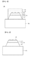
- FIG. 1 is a sectional view showing a light emitting device chip according to the first embodiment.
- the light emitting device 100 may include a light emitting structure 110, a transmittive layer 130 on the light emitting structure 110 and a luminescence material layer 140 on the transmittive layer 130.
- the luminescence material layer 140 may be provided in the light emitting device chip, so that the light emitting device chip can spontaneously generate white light.
- the transmittive layer 130 may have lower thermal conductivity and higher light transmittive property than the luminescence material layer 140.
- the transmittive layer 130 having low thermal conductivity and high light transmittive property may be interposed between a light emitting surface of the light emitting device chip and the luminescence material layer 140, so that heat generated from the light emitting surface of the light emitting structure 110 can be restricted from being transferred to the luminescence material layer 140, thereby improving the wavelength conversion efficiency of the luminescence material.
- the transmittive layer 130 may include silicon gel, but the embodiment is not limited thereto.
- the transmittive layer 130 may have a thickness of about 2 ⁇ m to 200 ⁇ m, but the embodiment is not limited thereto.
- the transmittive layer 130 may have a thickness of about 2 ⁇ m or above thicker than a first electrode 120 formed on the light emitting structure 110, but the embodiment is not limited thereto.
- the transmittive layer 130 may have a thickness of about 200 ⁇ m or below corresponding to the half of the total height of the light emitting device chip, but the embodiment is not limited thereto.
- the transmittive layer 130 may be formed on a top surface and a lateral side of the light emitting structure 110, but the embodiment is not limited thereto.
- the transmittive layer 130 may be exclusively formed on the top surface or the lateral side of the light emitting structure 110.
- the luminescence material layer 140 may have a thickness of about 5 ⁇ m to 500 ⁇ m, but the embodiment is not limited thereto.
- the luminescence material layer 140 may have a thickness of about 5 ⁇ m or above to convert blue light into yellow light or may have a thickness of about 500 ⁇ m or below by taking the size of the light emitting device chip into consideration, but the embodiment is not limited thereto.
- the first electrode 120 may include a line pattern having an electric connection and a part of the first electrode 120 may be electrically connected to an exposed pad electrode (not shown).
- the luminescence material layer 140 is provided in the light emitting device chip, so that the light emitting device chip can spontaneously generate white light.
- a lateral width of the light emitting structure 110 may be smaller than that of the second electrode 105, but the embodiment is not limited thereto.
- the heat generated from the light emitting device chip can be restricted from being transferred to the luminescence material layer 140, thereby improving the wavelength conversion efficiency of the luminescence material layer 140.
- the light emitting device chip may include the light emitting structure 110 formed on the second electrode 105.
- the second electrode 105 may include at least one of an ohmic layer, a reflective layer, a bonding layer and a conductive substrate.
- the light emitting structure 110 may include a second conductive semiconductor layer 116, an active layer 114 and a first conductive semiconductor layer 112.
- the first substrate may include a sapphire substrate or a SiC substrate, but the embodiment is not limited thereto.
- the light emitting structure 110 including the first conductive semiconductor layer 112, the active layer 114 and the second conductive semiconductor layer 116 is formed on the first substrate.
- the first conductive semiconductor layer 112 may include at least one selected from the group consisting of GaN, InN, AlN, InGaN, AlGaN, InAlGaN, AlInN, AlGaAs, InGaAs, AlInGaAs, GaP, AlGaP, InGaP, AlInGaP, InP.
- the first conductive semiconductor layer 112 may include an N type GaN layer, which is formed through the CVD, MBE, sputtering or HVPE.
- the first conductive semiconductor layer 112 can be formed by injecting trimethyl gallium (TMGa) gas, ammonia (NH 3 ) gas, nitrogen (N 2 ) gas and silane (SiH 4 ) gas including n type impurities, such as silicon, into the chamber.
- TMGa trimethyl gallium
- NH 3 ammonia
- N 2 nitrogen
- SiH 4 silane
- an undoped semiconductor layer (not shown) is formed on the first substrate (not shown) and the first conductive semiconductor layer 112 is formed on the undoped semiconductor layer in order to attenuate the lattice mismatch between the first substrate and the light emitting structure.
- the active layer 114 may include at least one of a single quantum well structure, a multiple quantum well (MQW) structure, a quantum wire structure or a quantum dot structure.
- MQW multiple quantum well
- the active layer 114 can be formed with the MQW structure by injecting TMGa gas, NH 3 gas, N 2 gas, and trimethyl indium (TMIn) gas, but the embodiment is not limited thereto.
- the active layer 114 may have a well/barrier layer including at least one of InGaN/GaN, InGaN/InGaN, AlGaN/GaN, InAlGaN/GaN, GaAs/AlGaAs (InGaAs) and GaP/AlGaP (InGaP), but the embodiment is not limited thereto.
- the well layer may include a material having the band gap energy lower than that of the barrier layer.
- the conductive clad layer can be formed on and/or under the active layer 114.
- the conductive clad layer may include an AlGaN-based semiconductor having the band gap energy higher than that of the active layer 114.
- the second conductive semiconductor layer 116 includes the group III-V compound semiconductor doped with the second conductive dopant.
- the second conductive semiconductor layer 116 may include the semiconductor material having the compositional formula of In x Al y Ga l - x-y N (0 ⁇ x ⁇ 1, 0 ⁇ y ⁇ 1, 0 ⁇ x+y ⁇ 1).
- the second conductive semiconductor layer 116 may include one selected from the group consisting of GaN, AlN, AlGaN, InGaN, InN, InAlGaN, AlInN, AlGaAs, GaP, GaAs, GaAsP, and AlGaInP.
- the second conductive dopant includes the P type dopant such as Mg, Zn, Ca, Sr, or Ba.
- the second conductive semiconductor layer 116 can be prepared as a single layer or a multiple layer, but the embodiment is not limited thereto.
- the second conductive semiconductor layer 116 may include a p type GaN layer, which can be formed by injecting TMGa gas, NH 3 gas, N 2 gas and (EtCp 2 Mg) ⁇ Mg(C 2 H 5 C 5 H 4 ) 2 ⁇ gas including p type impurities (for example, Mg) into the chamber, but the embodiment is not limited thereto.
- the first conductive semiconductor layer 112 may include an N type semiconductor layer and the second conductive semiconductor layer 116 may include a P type semiconductor layer, but the embodiment is not limited thereto.
- a semiconductor layer such as an N type semiconductor layer (not shown) having polarity opposite to that of the second conductive semiconductor layer 116, can be formed on the second conductive semiconductor layer 116.
- the light emitting structure 110 may include one of an N-P junction structure, a P-N junction structure, an N-P-N junction structure, and a P-N-P junction structure.
- the second electrode 105 is formed on the second conductive semiconductor layer 116.
- the second electrode 105 may include an ohmic layer (not shown), a reflective layer (not shown), a bonding layer (not shown) and a second substrate (not shown).
- the second electrode 105 may include at least one of Ti, Cr, Ni, Al, Pt, Au, W, Mo and a semiconductor substrate doped with impurities.
- the second electrode 105 may include the ohmic layer.
- the ohmic layer can be prepared as a multiple layer by stacking single metal, a metal alloy, and metal oxide in order to facilitate the hole injection.
- the ohmic layer may include at least one selected from the group consisting of ITO (indium tin oxide), IZO (indium zinc oxide), IZTO (indium zinc tin oxide), IAZO (indium aluminum zinc oxide), IGZO (indium gallium zinc oxide), IGTO (indium gallium tin oxide), AZO (aluminum zinc oxide), ATO (antimony tin oxide), GZO (gallium zinc oxide), IZON (IZO nitride), AGZO (Al-Ga ZnO), IGZO (In-Ga ZnO), ZnO, IrOx, RuOx, NiO, RuOx/ITO, Ni/IrOx/Au, Ni/IrOx/Au
- the reflective layer may include a metal or a metal alloy including at least one selected from the group consisting of Ag, Ni, Al, Rh, Pd, Ir, Ru, Mg, Zn, Pt, Au and Hf.
- the reflective layer can be prepared as a multiple layer by using the above metal or metal alloy and transmissive conductive material, such as IZO, IZTO, IAZO, IGZO, IGTO, AZO, or ATO.
- the reflective layer may have the stack structure including IZO/Ni, AZO/Ag, IZO/Ag/Ni, or AZO/Ag/Ni.
- the reflective layer may serve as the bonding layer or the bonding layer may include at least one selected from the group consisting of Ti, Au, Sn, Ni, Cr, Ga, In, Bi, Cu, Ag and Ta.
- the second electrode 105 may include the second substrate.
- the second substrate may include a metal having superior electric conductivity, a metal alloy or conductive semiconductor material in order to facilitate the hole injection.
- the second substrate may include at least one selected from the group consisting of Cu, a Cu alloy, Au, Ni, Mo, Cu-W, and a carrier wafer, such as Si, Ge, GaAs, GaN, ZnO, SiGe, and SiC wafers.
- the second substrate can be formed through the electrochemical metal deposition scheme or the bonding scheme using a eutectic metal.
- the first substrate is removed such that the first conductive semiconductor layer 112 can be exposed.
- the first substrate can be removed through the laser lift off scheme or the chemical lift off scheme.
- the first substrate can be removed by physically grinding the first substrate.
- the light emitting structure 110 can be formed on the second electrode 105 shown in FIG.1 .
- the etching process can be performed with respect to the light emitting structure 110 such that the light emitting structure 110 may have an inclined inner sidewall, but the embodiment is not limited thereto.
- the first electrode 120 is formed on the light emitting structure 110.
- the first electrode 120 may include the line pattern having the electric connection.
- the first electrode 120 can be electrically connected to the pad electrode (not shown).
- the transmittive layer 130 is formed on the light emitting structure 110.
- a first pattern 310 is formed at a lateral side of the light emitting structure 110 and the transmittive layer 130 is formed by using the first pattern 310 as a barrier.
- the transmittive layer 130 may have a thickness of about 2 ⁇ m to 200 ⁇ m, but the embodiment is not limited thereto.
- the transmittive layer 130 may have a thickness of about 2 ⁇ m or above thicker than THE first electrode 120 formed on the light emitting structure 110, but the embodiment is not limited thereto.
- the transmittive layer 130 may have a thickness of about 200 ⁇ m or below corresponding to the half of the total height of the light emitting device chip, but the embodiment is not limited thereto.
- the transmittive layer 130 may include silicon gel, but the embodiment is not limited thereto.
- the transmittive layer 130 having low thermal conductivity and high light transmittive property is interposed between the light emitting surface of the light emitting device chip and the luminescence material layer 140, so that the heat generated from the light emitting surface of the light emitting structure 110 can be restricted from being transferred to the luminescence material layer 140, thereby improving the wavelength conversion efficiency of the luminescence material.
- the first pattern 310 may be removed and a second pattern 320 may be formed.
- the luminescence material layer 140 may be formed on the transmittive layer 130 by using the second pattern 320 as a barrier.
- the luminescence material layer 140 may have a thickness of about 5 ⁇ m to 500 ⁇ m, but the embodiment is not limited thereto.
- the luminescence material layer 140 may have a thickness of about 5 ⁇ m or above to convert blue light into yellow light or may have a thickness of about 500 ⁇ m or below by taking the size of the light emitting device chip into consideration, but the embodiment is not limited thereto.
- the luminescence material layer 140 may include an encapsulating material including the luminescence material to protect the chip and to improve the light extraction efficiency.
- the encapsulating material may include an epoxy encapsulating material or a silicon encapsulating material, but the embodiment is not limited thereto.
- the luminescence material may include a host material and an active material.
- the luminescence material may include the host material of yttrium aluminum garnet (YAG) or a silicate-based material and the active material of cesium (Ce) or europium (Eu), but the embodiment is not limited thereto.
- dispensing In order to encapsulate the encapsulating material, dispensing, casting molding, transfer molding, vacuum printing or screen printing can be performed.
- the second pattern 320 is removed, thereby providing the light emitting device chip 100 according to the first embodiment.
- the luminescence material layer 140 is provided in the light emitting device chip, so that the light emitting device chip can spontaneously generate white light.
- the heat generated from the light emitting device chip can be restricted from being transferred to the luminescence material layer, thereby improving the wavelength conversion efficiency of the luminescence material layer.
- FIG. 6 is a sectional view showing a light emitting device chip 102 according to the second embodiment.
- the second embodiment may adopt the technical features of the first embodiment.
- the luminescence material layer includes a first luminescence material layer 141 formed on the transmittive layer 130 and a second luminescence material layer 142 formed on a part or a whole area of lateral sides of the light emitting structure 110.
- the second luminescence material layer 142 formed on the whole area of lateral sides of the light emitting structure 110 is shown for illustrative purpose, the embodiment is not limited thereto.
- a third pattern (not shown) spaced part from the transmittive layer 130 is formed as a barrier to form the luminescence material layer 140, but the embodiment is not limited thereto.
- the proportion of light such as blue light emitted from the light emitting surface of the light emitting device chip and extracted through the lateral side of the transmittive layer, can be adjusted, so that the optical characteristics, such as the color temperature variation depending on the viewing angles, can be controlled.
- the first luminescence material layer 141 may have a first thickness T1 and the second luminescence material layer 142 may have a second thickness T2.
- the second thickness T2 is thicker than the first thickness T1 by two times or less.
- FIG. 6 shows the second thickness T2 thinner than the first thickness T1, this is illustrative purpose only. Actually, the second thickness T2 is defined as 0 ⁇ T2 ⁇ 2T1.
- the proportion of light extracted through the lateral side of the transmittive layer can be adjusted by adjusting the second thickness T2 of the second luminescence material layer 142, so that the optical characteristics, such as the color temperature variation depending on the viewing angles, can be controlled.
- the proportion of light extracted through the lateral side of the transmittive layer can be adjusted according to the proportion of the second luminescence material layer 142 formed on the part or the whole area of the lateral sides of the light emitting structure 110, so that the optical characteristics, such as the color temperature variation depending on the viewing angles, can be controlled.
- FIG. 7a is a sectional view showing a light emitting device chip 103 according to the third embodiment.
- the third embodiment may adopt the technical features of the first and second embodiments.
- a luminescence material layer 143 may include a patterned luminescence material layer.
- a predetermined patterning process is performed after the luminescence material layer has been formed, or the luminescence material layer is formed after a fourth pattern (not shown) has been formed and the fourth pattern is removed through the lift off scheme, but the embodiment is not limited thereto.
- the patterned luminescence material layer 143 is formed on the light emitting device chip, so that the light extraction area may be enlarged due to the patterned luminescence material layer 143, thereby improving the light extraction efficiency.
- the transmittive layer 130 may be partially exposed through the patterned luminescence material layer 143, but the embodiment is not limited thereto.
- the transmittive layer 130 and the light emitting structure 110 may be partially exposed through the patterned luminescence material layer 143.
- the patterned luminescence material layer 143 can also be formed on the lateral sides of the light emitting structure 110.
- the light emitted through the lateral sides of the light emitting structure 110 may be converted into the white light.
- the patterned luminescence material layer 143 may be formed on the part of the lateral sides of the light emitting structure 110, other that the whole area of the lateral sides of the light emitting structure 110, so that the color temperature of the light emitted from the light emitting device chip can be controlled by adjusting the thickness of the patterned luminescence material layer 143 formed on the lateral sides of the light emitting structure 110.
- the area of the patterned luminescence material layer 143 is adjusted within 30% to 90% based on the light emitting area of the light emitting device chip, so that the color temperature of the light emitted from the light emitting device can be controlled.
- FIG. 7b is a sectional view showing a light emitting device chip 104 according to the fourth embodiment.
- the fourth embodiment may adopt the technical features of the first to third embodiments.
- a patterned luminescence material layer 143b may not expose the transmittive layer 130.
- the patterned luminescence material layer 143b is formed on the light emitting device chip, so that the light extraction area may be enlarged due to the patterned luminescence material layer 143b, thereby improving the light extraction efficiency.
- FIG. 8a is a sectional view showing a light emitting device chip 200 according to the second embodiment.
- the fifth embodiment is an example of a lateral type light emitting device chip and may adopt the technical features of the first to fourth embodiments.
- the light emitting device chip 200 includes a light emitting structure 210 formed on a non-conductive substrate 205 and provided with a first conductive semiconductor layer 212, an active layer 214 and a second conductive semiconductor layer 216, a transmittive layer 230 on the light emitting structure 210, and a luminescence material layer 240 on the transmittive layer 230.
- a third electrode 222 is formed on the first conductive semiconductor layer 212 and a fourth electrode 226 is formed on the second conductive semiconductor layer 216.
- FIG. 8b is a sectional view showing a light emitting device chip 202 according to the sixth embodiment.
- the sixth embodiment may adopt the technical features of the first to fifth embodiments.
- the transmittive layer 230 may be partially exposed through a patterned luminescence material layer 240b, but the embodiment is not limited thereto.
- the transmittive layer 230 and the light emitting structure 210 may be partially exposed through the patterned luminescence material layer 240b.
- a PSS (patterned sapphire substrate) 207 is formed on the non-conductive substrate 205 to improve the light extraction efficiency.
- the luminescence material layer is formed in the light emitting device chip, so that the light emitting device chip can spontaneously generate the white light.
- the heat generated from the light emitting device chip can be restricted from being transferred to the luminescence material layer, thereby improving the wavelength conversion efficiency of the luminescence material layer.
- the luminescence material layer having various shapes can be formed, so that the optical characteristics, such as the color temperature variation depending on the viewing angles, can be controlled.
- the luminescence material layer is patterned on the light emitting device chip, so that the light extraction efficiency can be improved.
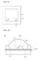
- FIG. 9 is a plan view showing the light emitting device chip according to the embodiment.
- the light emitting device chip further includes a pad electrode 125 electrically connected to the first electrode 120 and exposed upward of the transmittive layer 130.
- a pad electrode 125 electrically connected to the first electrode 120 and exposed upward of the transmittive layer 130.
- at least two pad electrodes 125 may be provided when the light emitting device has the mass storage, but the embodiment is not limited thereto.
- FIG. 10 is a view showing a light emitting device package 500 including the light emitting device chip according to the embodiments.
- the light emitting device package 500 includes a package body 505, fifth and sixth electrode layers 510 and 520 formed on the package body 505, the light emitting device chip 100 provided on the package body 505 and electrically connected to the fifth and sixth electrode layers 510 and 520 and a molding member 540 that surrounds the light emitting device chip 100.
- the package body 505 may include silicon, synthetic resin or a metallic material.
- An inclined surface may be formed around the light emitting device chip 100.
- the fifth and sixth electrode layers 510 and 520 are electrically isolated from each other to supply power to the light emitting device chip 100.
- the fifth and sixth electrode layers 510 and 520 reflect the light emitted from the light emitting device chip 100 to improve the light efficiency and dissipate heat generated from the light emitting device chip 100 to the outside.
- the light emitting device chips 100, 102, 103 and 200 according to first to fourth embodiments can be applied to the light emitting device package 500 and the light emitting device chip 100 can be installed on the package body 505 or the fifth or sixth electrode layer 510 or 520.
- the light emitting device chip 100 can be electrically connected to the fifth electrode layer 510 and/or the sixth electrode layer 520 through a wire 530. Although only one wire 530 is shown in FIG. 10 , the embodiment is not limited thereto. If the light emitting device chip according to the fourth embodiment is employed, a plurality of wires can be used.
- the molding member 540 surrounds the light emitting device chip 100 to protect the light emitting device chip 100.
- the luminescence material layer is provided in the light emitting device chip, so that the light emitting device chip can spontaneously generate white light.
- the heat generated from the light emitting device chip can be restricted from being transferred to the luminescence material layer, thereby improving the wavelength conversion efficiency of the luminescence material layer.
- the luminescence material layer having various shapes can be formed, so that the optical characteristics, such as the color temperature variation depending on the viewing angles, can be controlled.
- the luminescence material layer is patterned on the light emitting device chip, so that the light extraction efficiency can be improved.
- a plurality of light emitting device packages according to the embodiment may be arrayed on a substrate, and an optical member including a light guide plate, a prism sheet, a diffusion sheet or a fluorescent sheet may be provided on the optical path of the light emitted from the light emitting device package.
- the light emitting device package, the substrate, and the optical member may serve as a backlight unit or a lighting unit.
- the lighting system may include a backlight unit, a lighting unit, an indicator, a lamp or a streetlamp.
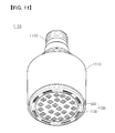
- FIG. 11 is a perspective view showing a lighting unit 1100 according to the embodiment.
- the lighting unit 1100 shown in FIG. 11 is an example of a lighting system and the embodiment is not limited thereto.
- the lighting unit 1100 includes a case body 1110, a light emitting module 1130 installed in the case body 1110, and a connection terminal 1120 installed in the case body 1110 to receive power from an external power source.
- the case body 1110 includes a material having superior heat dissipation property.
- the case body 1110 includes a metallic material or a resin material.
- the light emitting module 1130 may include a substrate 1132 and at least one light emitting device package 500 installed on the substrate 1132.
- the substrate 1132 includes an insulating member printed with a circuit pattern.
- the substrate 1132 includes a PCB (printed circuit board), an MC (metal core) PCB, an F (flexible) PCB, or a ceramic PCB.
- the substrate 1132 may include material that effectively reflects the light.
- the surface of the substrate 1132 can be coated with a color, such as a white color or a silver color, to effectively reflect the light.
- At least one light emitting device package 500 can be installed on the substrate 1132.
- Each light emitting device package 500 may include at least one LED (light emitting diode).
- the LED may include a colored LED that emits the light having the color of red, green, blue or white and a UV (ultraviolet) LED that emits UV light.
- the light emitting device packages 500 of the light emitting module 1130 can be variously combined to provide various colors and brightness.
- the white LED, the red LED and the green LED can be combined to achieve the high color rendering index (CRI).
- connection terminal 1120 is electrically connected to the light emitting module 1130 to supply power to the light emitting module 1130.
- the connection terminal 1120 has a shape of a socket screw-coupled with the external power source, but the embodiment is not limited thereto.
- the connection terminal 1120 can be prepared in the form of a pin inserted into the external power source or connected to the external power source through a wire.
- FIG. 12 is an exploded perspective view showing a backlight unit 1200 according to the embodiment.
- the backlight unit 1200 shown in FIG. 12 is an example of a lighting system and the embodiment is not limited thereto.
- the backlight unit 1200 includes a light guide plate 1210, a light emitting module 1240 for providing the light to the light guide plate 1210, a reflective member 1220 positioned below the light guide plate, and a bottom cover 1230 for receiving the light guide plate 1210, light emitting module 1240, and the reflective member 1220 therein, but the embodiment is not limited thereto.
- the light guide plate 1210 diffuses the light to provide surface light.
- the light guide 1210 includes transparent material.
- the light guide plate 1210 can be manufactured by using acryl-based resin, such as PMMA (polymethyl methacrylate), PET (polyethylene terephthalate), PC (polycarbonate), COC or PEN (polyethylene naphthalate) resin.
- PMMA polymethyl methacrylate
- PET polyethylene terephthalate
- PC polycarbonate
- COC polycarbonate
- PEN polyethylene naphthalate
- the light emitting module 1240 supplies the light to the lateral side of the light guide plate 1210 and serves as the light source of the display device including the backlight unit.
- the light emitting module 1240 can be positioned adjacent to the light guide plate 1210, but the embodiment is not limited thereto.
- the light emitting module 1240 includes a substrate 1242 and a plurality of light emitting device packages 500 installed on the substrate 1242 and the substrate 1242 can be adjacent to the light guide plate 1210, but the embodiment is not limited thereto.
- the substrate 1242 may include a printed circuit board (PCB) having a circuit pattern (not shown).
- the substrate 1242 may also include a metal core PCB (MCPCB) or a flexible PCB (FPCB), but the embodiment is not limited thereto.
- PCB printed circuit board
- MCPCB metal core PCB
- FPCB flexible PCB
- the light emitting device packages 500 are arranged such that light exit surfaces of the light emitting device packages 500 are spaced apart from the light guide plate 1210 by a predetermined distance.
- the reflective member 1220 is disposed below the light guide plate 1210.
- the reflective member 1220 reflects the light, which is travelled downward through the bottom surface of the light guide plate 1210, toward the light guide plate 1210, thereby improving the brightness of the backlight unit.
- the reflective member 1220 may include PET, PC or PVC resin, but the embodiment is not limited thereto.
- the bottom cover 1230 may receive the light guide plate 1210, the light emitting module 1240, and the reflective member 1220 therein. To this end, the bottom cover 1230 has a box shape with an open top surface, but the embodiment is not limited thereto.
- the bottom cover 1230 can be manufactured through a press process or an extrusion process by using metallic material or resin material.
- the luminescence material layer is provided in the light emitting device chip, so that the light emitting device chip can spontaneously generate white light.
- the heat generated from the light emitting device chip can be restricted from being transferred to the luminescence material layer, thereby improving the wavelength conversion efficiency of the luminescence material layer.
- the luminescence material layer having various shapes can be formed, so that the optical characteristics, such as the color temperature variation depending on the viewing angles, can be controlled.
- the luminescence material layer is patterned on the light emitting device chip, so that the light extraction efficiency can be improved.
- any reference in this specification to "one embodiment,” “an embodiment,” “example embodiment,” etc. means that a particular feature, structure, or characteristic described in connection with the embodiment is included in at least one embodiment of the invention.
- the appearances of such phrases in various places in the specification are not necessarily all referring to the same embodiment.
Landscapes
- Led Device Packages (AREA)
- Led Devices (AREA)
Abstract
Description
- The embodiment relates to a light emitting device chip, a light emitting device package, and a lighting system.
- A light emitting device includes a p-n junction diode having a characteristic of converting electric energy into light energy. The p-n junction diode can be formed by combining group III-V elements of the periodic table. The light emitting device can represent various colors by adjusting the compositional ratio of compound semiconductors.
- Meanwhile, in order to realize a white light emitting device package, light emitting devices representing red, green and blue colors, which are three primary colors of light, are combined with each other, the yellow luminescence material (YAG or TAG) is added to the blue light emitting device, or red/green/blue luminescence materials are employed in the UV light emitting device.
- Meanwhile, according to the white light emitting device package using the luminescence materials of the related art, a light emitting device chip is positioned on a bottom surface of a reflective cup, an encapsulating material mixed with the luminescence material is filled in the reflective cup, and the white light is formed by mixing the light having a first wavelength generated from the light emitting device chip with the light colliding with the luminescence material and having a wavelength longer than the first wavelength.
- However, according to the related art, the luminescence material mixed with the encapsulating material is filled in the reflective cup, so the reflective cup must be provided in the package.
- In addition, according to the related art, the light emitting device is adjacent to a luminescence material layer, so heat generated from the light emitting device is transferred to the luminescence material layer, thereby degrading the wavelength conversion efficiency of the luminescence material layer.
- Further, according to the related art, particles of the luminescence material may sink during the process, so the concentration of the luminescence material may vary depending on the process time.
- In addition, according to the related art, the color temperature variation may occur depending on the viewing angles.
- The embodiment provides a light emitting device chip, which can spontaneously generate white light by providing a luminescence material layer on a light emitting surface, a light emitting device package, and a lighting system.
- A light emitting device chip according to the embodiment may include a light emitting structure including a first conductive semiconductor layer, a second conductive semiconductor layer and an active layer interposed between the first and second conductive semiconductor layers; a transmittive layer on the light emitting structure; and a luminescence material layer on the transmittive layer, wherein the luminescence material layer includes a pattern, which does not expose the transmittive layer, partially exposes the transmittive layer or partially exposes the transmittive layer and the light emitting structure.
- A light emitting device chip according to the embodiment may include a light emitting structure including a first conductive semiconductor layer, a second conductive semiconductor layer and an active layer interposed between the first and second conductive semiconductor layers; a transmittive layer on the light emitting structure; and a luminescence material layer on the transmittive layer, wherein the transmittive layer is formed on a top surface and lateral sides of the light emitting structure.
- In addition, a light emitting device package according to the embodiment may include a package body; third and fourth electrode layers on the package body; and a light emitting device claimed in claim 1 or 8 and electrically connected to the third and fourth electrode layers.
- In addition, a lighting system according to the embodiment may include a light emitting module including a substrate and a light emitting device package on the substrate, wherein the light emitting device package includes a package body, at least one electrode layer on the package body and the light emitting device package electrically connected to the electrode layer.
-
-
FIG. 1 is a sectional view showing a light emitting device chip according to the first embodiment; -
FIGS. 2 to 5 are sectional views showing a method for manufacturing a light emitting device chip according to the first embodiment; -
FIG. 6 is a sectional view showing a light emitting device chip according to the second embodiment; -
FIG. 7a is a sectional view showing a light emitting device chip according to the third embodiment; -
FIG. 7b is a sectional view showing a light emitting device chip according to the fourth embodiment; -
FIG. 8a is a sectional view showing a light emitting device chip according to the fifth embodiment; -
FIG. 8b is a sectional view showing a light emitting device chip according to the sixth embodiment; -
FIG. 9 is a plan view showing a light emitting device chip according to the embodiment; -
FIG. 10 is a sectional view showing a light emitting device package according to the embodiment; -
FIG. 11 is a perspective view showing a lighting unit according to the embodiment; and -
FIG. 12 is an exploded perspective view showing a backlight unit according to the embodiment. - Hereinafter, a light emitting device chip, a light emitting device package, and a lighting system according to the embodiments will be described in detail with reference to accompanying drawings.
- In the description of embodiments, it will be understood that when a layer (or film) is referred to as being 'on' another layer or substrate, it can be directly on another layer or substrate, or intervening layers may also be present. Further, it will be understood that when a layer is referred to as being 'under' another layer, it can be directly under another layer, and one or more intervening layers may also be present. In addition, it will also be understood that when a layer is referred to as being 'between' two layers, it can be the only layer between the two layers, or one or more intervening layers may also be present.
-
FIG. 1 is a sectional view showing a light emitting device chip according to the first embodiment. - The
light emitting device 100 according to the embodiment may include alight emitting structure 110, atransmittive layer 130 on thelight emitting structure 110 and aluminescence material layer 140 on thetransmittive layer 130. - According to the light emitting device chip of the embodiment, the
luminescence material layer 140 may be provided in the light emitting device chip, so that the light emitting device chip can spontaneously generate white light. - According to the embodiment, the
transmittive layer 130 may have lower thermal conductivity and higher light transmittive property than theluminescence material layer 140. - In addition, according to the embodiment, the
transmittive layer 130 having low thermal conductivity and high light transmittive property may be interposed between a light emitting surface of the light emitting device chip and theluminescence material layer 140, so that heat generated from the light emitting surface of thelight emitting structure 110 can be restricted from being transferred to theluminescence material layer 140, thereby improving the wavelength conversion efficiency of the luminescence material. - The
transmittive layer 130 may include silicon gel, but the embodiment is not limited thereto. - The
transmittive layer 130 may have a thickness of about 2 µm to 200 µm, but the embodiment is not limited thereto. For instance, thetransmittive layer 130 may have a thickness of about 2 µm or above thicker than afirst electrode 120 formed on thelight emitting structure 110, but the embodiment is not limited thereto. In addition, thetransmittive layer 130 may have a thickness of about 200 µm or below corresponding to the half of the total height of the light emitting device chip, but the embodiment is not limited thereto. - The
transmittive layer 130 may be formed on a top surface and a lateral side of thelight emitting structure 110, but the embodiment is not limited thereto. For instance, thetransmittive layer 130 may be exclusively formed on the top surface or the lateral side of thelight emitting structure 110. - The
luminescence material layer 140 may have a thickness of about 5 µm to 500 µm, but the embodiment is not limited thereto. For instance, theluminescence material layer 140 may have a thickness of about 5 µm or above to convert blue light into yellow light or may have a thickness of about 500 µm or below by taking the size of the light emitting device chip into consideration, but the embodiment is not limited thereto. - According to the embodiment, the
first electrode 120 may include a line pattern having an electric connection and a part of thefirst electrode 120 may be electrically connected to an exposed pad electrode (not shown). - According to the embodiment, the
luminescence material layer 140 is provided in the light emitting device chip, so that the light emitting device chip can spontaneously generate white light. - According to the embodiment, a lateral width of the
light emitting structure 110 may be smaller than that of thesecond electrode 105, but the embodiment is not limited thereto. - In addition, according to the embodiment, the heat generated from the light emitting device chip can be restricted from being transferred to the
luminescence material layer 140, thereby improving the wavelength conversion efficiency of theluminescence material layer 140. - Hereinafter, the method for manufacturing the light emitting device chip according to the first embodiment will be described with reference to
FIGS. 2 to 5 . - As shown in
FIG. 2 , the light emitting device chip according to the first embodiment may include thelight emitting structure 110 formed on thesecond electrode 105. Thesecond electrode 105 may include at least one of an ohmic layer, a reflective layer, a bonding layer and a conductive substrate. - The
light emitting structure 110 may include a secondconductive semiconductor layer 116, anactive layer 114 and a firstconductive semiconductor layer 112. - Hereinafter, the method of forming the
light emitting structure 110 on thesecond electrode 105 will be described. - First, a first substrate (not shown) is prepared. The first substrate may include a sapphire substrate or a SiC substrate, but the embodiment is not limited thereto.
- Then, the
light emitting structure 110 including the firstconductive semiconductor layer 112, theactive layer 114 and the secondconductive semiconductor layer 116 is formed on the first substrate. - The first
conductive semiconductor layer 112 may include at least one selected from the group consisting of GaN, InN, AlN, InGaN, AlGaN, InAlGaN, AlInN, AlGaAs, InGaAs, AlInGaAs, GaP, AlGaP, InGaP, AlInGaP, InP. - The first
conductive semiconductor layer 112 may include an N type GaN layer, which is formed through the CVD, MBE, sputtering or HVPE. In addition, the firstconductive semiconductor layer 112 can be formed by injecting trimethyl gallium (TMGa) gas, ammonia (NH3) gas, nitrogen (N2) gas and silane (SiH4) gas including n type impurities, such as silicon, into the chamber. - According to the embodiment, an undoped semiconductor layer (not shown) is formed on the first substrate (not shown) and the first
conductive semiconductor layer 112 is formed on the undoped semiconductor layer in order to attenuate the lattice mismatch between the first substrate and the light emitting structure. - The
active layer 114 may include at least one of a single quantum well structure, a multiple quantum well (MQW) structure, a quantum wire structure or a quantum dot structure. For instance, theactive layer 114 can be formed with the MQW structure by injecting TMGa gas, NH3 gas, N2 gas, and trimethyl indium (TMIn) gas, but the embodiment is not limited thereto. - The
active layer 114 may have a well/barrier layer including at least one of InGaN/GaN, InGaN/InGaN, AlGaN/GaN, InAlGaN/GaN, GaAs/AlGaAs (InGaAs) and GaP/AlGaP (InGaP), but the embodiment is not limited thereto. The well layer may include a material having the band gap energy lower than that of the barrier layer. - The conductive clad layer can be formed on and/or under the
active layer 114. The conductive clad layer may include an AlGaN-based semiconductor having the band gap energy higher than that of theactive layer 114. - The second
conductive semiconductor layer 116 includes the group III-V compound semiconductor doped with the second conductive dopant. For instance, the secondconductive semiconductor layer 116 may include the semiconductor material having the compositional formula of InxAlyGal-x-yN (0≤x≤1, 0≤y≤1, 0≤x+y≤1). In detail, the secondconductive semiconductor layer 116 may include one selected from the group consisting of GaN, AlN, AlGaN, InGaN, InN, InAlGaN, AlInN, AlGaAs, GaP, GaAs, GaAsP, and AlGaInP. If the secondconductive semiconductor layer 116 is a P type semiconductor layer, the second conductive dopant includes the P type dopant such as Mg, Zn, Ca, Sr, or Ba. The secondconductive semiconductor layer 116 can be prepared as a single layer or a multiple layer, but the embodiment is not limited thereto. - The second
conductive semiconductor layer 116 may include a p type GaN layer, which can be formed by injecting TMGa gas, NH3 gas, N2 gas and (EtCp2Mg){Mg(C2H5C5H4)2} gas including p type impurities (for example, Mg) into the chamber, but the embodiment is not limited thereto. - According to the embodiment, the first
conductive semiconductor layer 112 may include an N type semiconductor layer and the secondconductive semiconductor layer 116 may include a P type semiconductor layer, but the embodiment is not limited thereto. In addition, a semiconductor layer, such as an N type semiconductor layer (not shown) having polarity opposite to that of the secondconductive semiconductor layer 116, can be formed on the secondconductive semiconductor layer 116. Thus, thelight emitting structure 110 may include one of an N-P junction structure, a P-N junction structure, an N-P-N junction structure, and a P-N-P junction structure. - After that, the
second electrode 105 is formed on the secondconductive semiconductor layer 116. - The
second electrode 105 may include an ohmic layer (not shown), a reflective layer (not shown), a bonding layer (not shown) and a second substrate (not shown). Thesecond electrode 105 may include at least one of Ti, Cr, Ni, Al, Pt, Au, W, Mo and a semiconductor substrate doped with impurities. - For instance, the
second electrode 105 may include the ohmic layer. In this case, the ohmic layer can be prepared as a multiple layer by stacking single metal, a metal alloy, and metal oxide in order to facilitate the hole injection. For instance, the ohmic layer may include at least one selected from the group consisting of ITO (indium tin oxide), IZO (indium zinc oxide), IZTO (indium zinc tin oxide), IAZO (indium aluminum zinc oxide), IGZO (indium gallium zinc oxide), IGTO (indium gallium tin oxide), AZO (aluminum zinc oxide), ATO (antimony tin oxide), GZO (gallium zinc oxide), IZON (IZO nitride), AGZO (Al-Ga ZnO), IGZO (In-Ga ZnO), ZnO, IrOx, RuOx, NiO, RuOx/ITO, Ni/IrOx/Au, Ni/IrOx/Au/ITO, Ag, Ni, Cr, Ti, Al, Rh, Pd, Ir, Ru, Mg, Zn, Pt, Au, and Hf, but the embodiment is not limited thereto. - When the
second electrode 105 includes the reflective layer, the reflective layer may include a metal or a metal alloy including at least one selected from the group consisting of Ag, Ni, Al, Rh, Pd, Ir, Ru, Mg, Zn, Pt, Au and Hf. In addition, the reflective layer can be prepared as a multiple layer by using the above metal or metal alloy and transmissive conductive material, such as IZO, IZTO, IAZO, IGZO, IGTO, AZO, or ATO. For instance, the reflective layer may have the stack structure including IZO/Ni, AZO/Ag, IZO/Ag/Ni, or AZO/Ag/Ni. - In addition, if the
second electrode layer 120 includes the bonding layer, the reflective layer may serve as the bonding layer or the bonding layer may include at least one selected from the group consisting of Ti, Au, Sn, Ni, Cr, Ga, In, Bi, Cu, Ag and Ta. - In addition, the
second electrode 105 may include the second substrate. The second substrate may include a metal having superior electric conductivity, a metal alloy or conductive semiconductor material in order to facilitate the hole injection. For instance, the second substrate may include at least one selected from the group consisting of Cu, a Cu alloy, Au, Ni, Mo, Cu-W, and a carrier wafer, such as Si, Ge, GaAs, GaN, ZnO, SiGe, and SiC wafers. - The second substrate can be formed through the electrochemical metal deposition scheme or the bonding scheme using a eutectic metal.
- Then, the first substrate is removed such that the first
conductive semiconductor layer 112 can be exposed. The first substrate can be removed through the laser lift off scheme or the chemical lift off scheme. In addition, the first substrate can be removed by physically grinding the first substrate. - Thus, the
light emitting structure 110 can be formed on thesecond electrode 105 shown inFIG.1 . - After the first substrate has been removed, the etching process can be performed with respect to the
light emitting structure 110 such that thelight emitting structure 110 may have an inclined inner sidewall, but the embodiment is not limited thereto. - Then, the
first electrode 120 is formed on thelight emitting structure 110. Thefirst electrode 120 may include the line pattern having the electric connection. Thefirst electrode 120 can be electrically connected to the pad electrode (not shown). - After that, as shown in
FIG. 3 , thetransmittive layer 130 is formed on thelight emitting structure 110. - For instance, a
first pattern 310 is formed at a lateral side of thelight emitting structure 110 and thetransmittive layer 130 is formed by using thefirst pattern 310 as a barrier. - The
transmittive layer 130 may have a thickness of about 2 µm to 200 µm, but the embodiment is not limited thereto. For instance, thetransmittive layer 130 may have a thickness of about 2 µm or above thicker than THEfirst electrode 120 formed on thelight emitting structure 110, but the embodiment is not limited thereto. In addition, thetransmittive layer 130 may have a thickness of about 200 µm or below corresponding to the half of the total height of the light emitting device chip, but the embodiment is not limited thereto. - The
transmittive layer 130 may include silicon gel, but the embodiment is not limited thereto. - According to the embodiment, the
transmittive layer 130 having low thermal conductivity and high light transmittive property is interposed between the light emitting surface of the light emitting device chip and theluminescence material layer 140, so that the heat generated from the light emitting surface of thelight emitting structure 110 can be restricted from being transferred to theluminescence material layer 140, thereby improving the wavelength conversion efficiency of the luminescence material. - Then, as shown in
FIG. 4 , thefirst pattern 310 may be removed and asecond pattern 320 may be formed. After that, theluminescence material layer 140 may be formed on thetransmittive layer 130 by using thesecond pattern 320 as a barrier. - The
luminescence material layer 140 may have a thickness of about 5 µm to 500 µm, but the embodiment is not limited thereto. For instance, theluminescence material layer 140 may have a thickness of about 5 µm or above to convert blue light into yellow light or may have a thickness of about 500 µm or below by taking the size of the light emitting device chip into consideration, but the embodiment is not limited thereto. - The
luminescence material layer 140 may include an encapsulating material including the luminescence material to protect the chip and to improve the light extraction efficiency. - The encapsulating material may include an epoxy encapsulating material or a silicon encapsulating material, but the embodiment is not limited thereto.
- The luminescence material may include a host material and an active material. For instance, the luminescence material may include the host material of yttrium aluminum garnet (YAG) or a silicate-based material and the active material of cesium (Ce) or europium (Eu), but the embodiment is not limited thereto.
- In order to encapsulate the encapsulating material, dispensing, casting molding, transfer molding, vacuum printing or screen printing can be performed.
- After that, as shown in
FIG. 5 , thesecond pattern 320 is removed, thereby providing the light emittingdevice chip 100 according to the first embodiment. - According to the light emitting device chip of the embodiment, the
luminescence material layer 140 is provided in the light emitting device chip, so that the light emitting device chip can spontaneously generate white light. - In addition, according to the embodiment, the heat generated from the light emitting device chip can be restricted from being transferred to the luminescence material layer, thereby improving the wavelength conversion efficiency of the luminescence material layer.
-
FIG. 6 is a sectional view showing a light emittingdevice chip 102 according to the second embodiment. - The second embodiment may adopt the technical features of the first embodiment.
- According to the second embodiment, the luminescence material layer includes a first
luminescence material layer 141 formed on thetransmittive layer 130 and a secondluminescence material layer 142 formed on a part or a whole area of lateral sides of thelight emitting structure 110. Although the secondluminescence material layer 142 formed on the whole area of lateral sides of thelight emitting structure 110 is shown for illustrative purpose, the embodiment is not limited thereto. - According to the second embodiment, after the
transmittive layer 130 is formed, a third pattern (not shown) spaced part from thetransmittive layer 130 is formed as a barrier to form theluminescence material layer 140, but the embodiment is not limited thereto. - According to the second embodiment, the proportion of light, such as blue light emitted from the light emitting surface of the light emitting device chip and extracted through the lateral side of the transmittive layer, can be adjusted, so that the optical characteristics, such as the color temperature variation depending on the viewing angles, can be controlled.
- For instance, the first
luminescence material layer 141 may have a first thickness T1 and the secondluminescence material layer 142 may have a second thickness T2. - According to the second embodiment, the second thickness T2 is thicker than the first thickness T1 by two times or less. Although
FIG. 6 shows the second thickness T2 thinner than the first thickness T1, this is illustrative purpose only. Actually, the second thickness T2 is defined as 0 < T2≤2T1. - According to the second embodiment, the proportion of light extracted through the lateral side of the transmittive layer can be adjusted by adjusting the second thickness T2 of the second
luminescence material layer 142, so that the optical characteristics, such as the color temperature variation depending on the viewing angles, can be controlled. - In addition, according to the second embodiment, the proportion of light extracted through the lateral side of the transmittive layer can be adjusted according to the proportion of the second
luminescence material layer 142 formed on the part or the whole area of the lateral sides of thelight emitting structure 110, so that the optical characteristics, such as the color temperature variation depending on the viewing angles, can be controlled. -
FIG. 7a is a sectional view showing a light emittingdevice chip 103 according to the third embodiment. - The third embodiment may adopt the technical features of the first and second embodiments.
- According to the third embodiment, a
luminescence material layer 143 may include a patterned luminescence material layer. - According to the third embodiment, similar to the first embodiment, a predetermined patterning process is performed after the luminescence material layer has been formed, or the luminescence material layer is formed after a fourth pattern (not shown) has been formed and the fourth pattern is removed through the lift off scheme, but the embodiment is not limited thereto.
- According to the third embodiment, the patterned
luminescence material layer 143 is formed on the light emitting device chip, so that the light extraction area may be enlarged due to the patternedluminescence material layer 143, thereby improving the light extraction efficiency. - According to the third embodiment, as shown in
FIG. 7a , thetransmittive layer 130 may be partially exposed through the patternedluminescence material layer 143, but the embodiment is not limited thereto. In addition, thetransmittive layer 130 and thelight emitting structure 110 may be partially exposed through the patternedluminescence material layer 143. - In addition, according to the third embodiment, the patterned
luminescence material layer 143 can also be formed on the lateral sides of thelight emitting structure 110. Thus, the light emitted through the lateral sides of thelight emitting structure 110 may be converted into the white light. In addition, the patternedluminescence material layer 143 may be formed on the part of the lateral sides of thelight emitting structure 110, other that the whole area of the lateral sides of thelight emitting structure 110, so that the color temperature of the light emitted from the light emitting device chip can be controlled by adjusting the thickness of the patternedluminescence material layer 143 formed on the lateral sides of thelight emitting structure 110. - According to the third embodiment, the area of the patterned
luminescence material layer 143 is adjusted within 30% to 90% based on the light emitting area of the light emitting device chip, so that the color temperature of the light emitted from the light emitting device can be controlled. -
FIG. 7b is a sectional view showing a light emittingdevice chip 104 according to the fourth embodiment. - The fourth embodiment may adopt the technical features of the first to third embodiments.
- In the light emitting
device chip 104 according to the fourth embodiment, a patternedluminescence material layer 143b may not expose thetransmittive layer 130. - According to the fourth embodiment, the patterned
luminescence material layer 143b is formed on the light emitting device chip, so that the light extraction area may be enlarged due to the patternedluminescence material layer 143b, thereby improving the light extraction efficiency. -
FIG. 8a is a sectional view showing a light emittingdevice chip 200 according to the second embodiment. - The fifth embodiment is an example of a lateral type light emitting device chip and may adopt the technical features of the first to fourth embodiments.
- The light emitting
device chip 200 according to the fifth embodiment includes alight emitting structure 210 formed on anon-conductive substrate 205 and provided with a firstconductive semiconductor layer 212, anactive layer 214 and a secondconductive semiconductor layer 216, atransmittive layer 230 on thelight emitting structure 210, and aluminescence material layer 240 on thetransmittive layer 230. Athird electrode 222 is formed on the firstconductive semiconductor layer 212 and afourth electrode 226 is formed on the secondconductive semiconductor layer 216. -
FIG. 8b is a sectional view showing a light emittingdevice chip 202 according to the sixth embodiment. - The sixth embodiment may adopt the technical features of the first to fifth embodiments.
- According to the sixth embodiment, the
transmittive layer 230 may be partially exposed through a patternedluminescence material layer 240b, but the embodiment is not limited thereto. In addition, thetransmittive layer 230 and thelight emitting structure 210 may be partially exposed through the patternedluminescence material layer 240b. - In addition, according to the sixth embodiment, a PSS (patterned sapphire substrate) 207 is formed on the
non-conductive substrate 205 to improve the light extraction efficiency. - According to the light emitting device chip, the light emitting device package and the method of manufacturing the light emitting device chip of the embodiments, the luminescence material layer is formed in the light emitting device chip, so that the light emitting device chip can spontaneously generate the white light.
- In addition, according to the embodiment, the heat generated from the light emitting device chip can be restricted from being transferred to the luminescence material layer, thereby improving the wavelength conversion efficiency of the luminescence material layer.
- Further, according to the embodiment, the luminescence material layer having various shapes can be formed, so that the optical characteristics, such as the color temperature variation depending on the viewing angles, can be controlled.
- In addition, according to the embodiment, the luminescence material layer is patterned on the light emitting device chip, so that the light extraction efficiency can be improved.
-
FIG. 9 is a plan view showing the light emitting device chip according to the embodiment. - According to the present embodiment, the light emitting device chip further includes a
pad electrode 125 electrically connected to thefirst electrode 120 and exposed upward of thetransmittive layer 130. For instance, in the case of the vertical type light emitting device, at least twopad electrodes 125 may be provided when the light emitting device has the mass storage, but the embodiment is not limited thereto. -
FIG. 10 is a view showing a light emittingdevice package 500 including the light emitting device chip according to the embodiments. - The light emitting
device package 500 according to the embodiment includes apackage body 505, fifth and sixth electrode layers 510 and 520 formed on thepackage body 505, the light emittingdevice chip 100 provided on thepackage body 505 and electrically connected to the fifth and sixth electrode layers 510 and 520 and amolding member 540 that surrounds the light emittingdevice chip 100. - The
package body 505 may include silicon, synthetic resin or a metallic material. An inclined surface may be formed around the light emittingdevice chip 100. - The fifth and sixth electrode layers 510 and 520 are electrically isolated from each other to supply power to the light emitting
device chip 100. In addition, the fifth and sixth electrode layers 510 and 520 reflect the light emitted from the light emittingdevice chip 100 to improve the light efficiency and dissipate heat generated from the light emittingdevice chip 100 to the outside. - The light emitting
device chips device package 500 and the light emittingdevice chip 100 can be installed on thepackage body 505 or the fifth orsixth electrode layer - The light emitting
device chip 100 can be electrically connected to thefifth electrode layer 510 and/or thesixth electrode layer 520 through awire 530. Although only onewire 530 is shown inFIG. 10 , the embodiment is not limited thereto. If the light emitting device chip according to the fourth embodiment is employed, a plurality of wires can be used. - The
molding member 540 surrounds the light emittingdevice chip 100 to protect the light emittingdevice chip 100. - According to the light emitting device chip and the light emitting device package of the embodiment, the luminescence material layer is provided in the light emitting device chip, so that the light emitting device chip can spontaneously generate white light.
- In addition, according to the embodiment, the heat generated from the light emitting device chip can be restricted from being transferred to the luminescence material layer, thereby improving the wavelength conversion efficiency of the luminescence material layer.
- Further, according to the embodiment, the luminescence material layer having various shapes can be formed, so that the optical characteristics, such as the color temperature variation depending on the viewing angles, can be controlled.
- In addition, according to the embodiment, the luminescence material layer is patterned on the light emitting device chip, so that the light extraction efficiency can be improved.
- A plurality of light emitting device packages according to the embodiment may be arrayed on a substrate, and an optical member including a light guide plate, a prism sheet, a diffusion sheet or a fluorescent sheet may be provided on the optical path of the light emitted from the light emitting device package. The light emitting device package, the substrate, and the optical member may serve as a backlight unit or a lighting unit. For instance, the lighting system may include a backlight unit, a lighting unit, an indicator, a lamp or a streetlamp.
-
FIG. 11 is a perspective view showing alighting unit 1100 according to the embodiment. Thelighting unit 1100 shown inFIG. 11 is an example of a lighting system and the embodiment is not limited thereto. - Referring to
FIG. 11 , thelighting unit 1100 includes acase body 1110, alight emitting module 1130 installed in thecase body 1110, and aconnection terminal 1120 installed in thecase body 1110 to receive power from an external power source. - Preferably, the
case body 1110 includes a material having superior heat dissipation property. For instance, thecase body 1110 includes a metallic material or a resin material. - The
light emitting module 1130 may include asubstrate 1132 and at least one light emittingdevice package 500 installed on thesubstrate 1132. - The
substrate 1132 includes an insulating member printed with a circuit pattern. For instance, thesubstrate 1132 includes a PCB (printed circuit board), an MC (metal core) PCB, an F (flexible) PCB, or a ceramic PCB. - In addition, the
substrate 1132 may include material that effectively reflects the light. The surface of thesubstrate 1132 can be coated with a color, such as a white color or a silver color, to effectively reflect the light. - At least one light emitting
device package 500 can be installed on thesubstrate 1132. Each light emittingdevice package 500 may include at least one LED (light emitting diode). The LED may include a colored LED that emits the light having the color of red, green, blue or white and a UV (ultraviolet) LED that emits UV light. - The light emitting device packages 500 of the
light emitting module 1130 can be variously combined to provide various colors and brightness. For instance, the white LED, the red LED and the green LED can be combined to achieve the high color rendering index (CRI). - The
connection terminal 1120 is electrically connected to thelight emitting module 1130 to supply power to thelight emitting module 1130. Referring toFIG. 11 , theconnection terminal 1120 has a shape of a socket screw-coupled with the external power source, but the embodiment is not limited thereto. For instance, theconnection terminal 1120 can be prepared in the form of a pin inserted into the external power source or connected to the external power source through a wire. -
FIG. 12 is an exploded perspective view showing abacklight unit 1200 according to the embodiment. Thebacklight unit 1200 shown inFIG. 12 is an example of a lighting system and the embodiment is not limited thereto. - The
backlight unit 1200 according to the embodiment includes alight guide plate 1210, alight emitting module 1240 for providing the light to thelight guide plate 1210, areflective member 1220 positioned below the light guide plate, and abottom cover 1230 for receiving thelight guide plate 1210, light emittingmodule 1240, and thereflective member 1220 therein, but the embodiment is not limited thereto. - The
light guide plate 1210 diffuses the light to provide surface light. Thelight guide 1210 includes transparent material. For instance, thelight guide plate 1210 can be manufactured by using acryl-based resin, such as PMMA (polymethyl methacrylate), PET (polyethylene terephthalate), PC (polycarbonate), COC or PEN (polyethylene naphthalate) resin. - The
light emitting module 1240 supplies the light to the lateral side of thelight guide plate 1210 and serves as the light source of the display device including the backlight unit. - The
light emitting module 1240 can be positioned adjacent to thelight guide plate 1210, but the embodiment is not limited thereto. In detail, thelight emitting module 1240 includes asubstrate 1242 and a plurality of light emitting device packages 500 installed on thesubstrate 1242 and thesubstrate 1242 can be adjacent to thelight guide plate 1210, but the embodiment is not limited thereto. - The
substrate 1242 may include a printed circuit board (PCB) having a circuit pattern (not shown). In addition, thesubstrate 1242 may also include a metal core PCB (MCPCB) or a flexible PCB (FPCB), but the embodiment is not limited thereto. - In addition, the light emitting device packages 500 are arranged such that light exit surfaces of the light emitting device packages 500 are spaced apart from the
light guide plate 1210 by a predetermined distance. - The
reflective member 1220 is disposed below thelight guide plate 1210. Thereflective member 1220 reflects the light, which is travelled downward through the bottom surface of thelight guide plate 1210, toward thelight guide plate 1210, thereby improving the brightness of the backlight unit. For instance, thereflective member 1220 may include PET, PC or PVC resin, but the embodiment is not limited thereto. - The
bottom cover 1230 may receive thelight guide plate 1210, thelight emitting module 1240, and thereflective member 1220 therein. To this end, thebottom cover 1230 has a box shape with an open top surface, but the embodiment is not limited thereto. - The
bottom cover 1230 can be manufactured through a press process or an extrusion process by using metallic material or resin material. - According to the light emitting device chip, the light emitting device package and the lighting system of the embodiment, the luminescence material layer is provided in the light emitting device chip, so that the light emitting device chip can spontaneously generate white light.
- In addition, according to the embodiment, the heat generated from the light emitting device chip can be restricted from being transferred to the luminescence material layer, thereby improving the wavelength conversion efficiency of the luminescence material layer.
- Further, according to the embodiment, the luminescence material layer having various shapes can be formed, so that the optical characteristics, such as the color temperature variation depending on the viewing angles, can be controlled.
- In addition, according to the embodiment, the luminescence material layer is patterned on the light emitting device chip, so that the light extraction efficiency can be improved.
- Any reference in this specification to "one embodiment," "an embodiment," "example embodiment," etc., means that a particular feature, structure, or characteristic described in connection with the embodiment is included in at least one embodiment of the invention. The appearances of such phrases in various places in the specification are not necessarily all referring to the same embodiment. Further, when a particular feature, structure, or characteristic is described in connection with any embodiment, it is submitted that it is within the purview of one skilled in the art to effect such feature, structure, or characteristic in connection with other ones of the embodiments.
- Although embodiments have been described with reference to a number of illustrative embodiments thereof, it should be understood that numerous other modifications and embodiments can be devised by those skilled in the art that will fall within the spirit and scope of the principles of this disclosure. More particularly, various variations and modifications are possible in the component parts and/or arrangements of the subject combination arrangement within the scope of the disclosure, the drawings and the appended claims. In addition to variations and modifications in the component parts and/or arrangements, alternative uses will also be apparent to those skilled in the art.
Claims (15)
- A light emitting device chip comprising:a light emitting structure including a first conductive semiconductor layer, a second conductive semiconductor layer and an active layer interposed between the first and second conductive semiconductor layers;a transmittive layer on the light emitting structure; anda luminescence material layer on the transmittive layer,wherein the luminescence material layer comprises a pattern.
- The light emitting device chip of claim 1, wherein the luminescence material layer does not expose the transmittive layer.
- The light emitting device chip of claim 1, wherein the luminescence material layer partially exposes the transmittive layer.
- The light emitting device chip of claim 1, wherein the luminescence material layer partially exposes the transmittive layer and the light emitting structure
- The light emitting device chip of claim 1, wherein the luminescence material layer is formed on a part or a whole area of lateral sides of the light emitting structure.
- The light emitting device chip of claim 1, wherein the transmittive layer has a thickness of 2 µm to 200 µm.
- The light emitting device chip of claim 1, wherein the luminescence material layer has a thickness of 5 µm to 500 µm.
- The light emitting device chip of claim 1, wherein an area of the luminescence material layer remaining after a patterning process is in a range of 30% to 90% based on a light emitting area of the light emitting device chip.
- The light emitting device chip of claim 5, wherein the luminescence material layer at the lateral sides of the light emitting structure comprises the pattern.
- The light emitting device chip of claim 5, wherein a thickness of the luminescence material layer at the lateral sides of the light emitting structure is thicker than a thickness of the luminescence material layer formed on the transmittive layer by two times or less.
- The light emitting device chip of claim 1, wherein the transmittive layer is formed on a top surface and lateral sides of the light emitting structure.
- The light emitting device chip of claim 1, further comprising a sapphire substrate; and a patterned sapphire substrate on the sapphire substrate.
- The light emitting device chip of claim 1, wherein the transmittive layer comprises a silicon gel.
- The light emitting device chip of claim 1, the transmittive layer has a lower thermal conductivity and a higher light transmittive property than the luminescence material layer.
- A light emitting device package comprising:a package body;third and fourth electrode layers on the package body; anda light emitting device claimed in any one claim of claims 1 to 14 and electrically connected to the third and fourth electrode layers.
Applications Claiming Priority (1)
| Application Number | Priority Date | Filing Date | Title |
|---|---|---|---|
| KR20100003544A KR101007145B1 (en) | 2010-01-14 | 2010-01-14 | Method of manufacturing light emitting device chip, light emitting device package and light emitting device chip |
Publications (3)
| Publication Number | Publication Date |
|---|---|
| EP2346102A2 true EP2346102A2 (en) | 2011-07-20 |
| EP2346102A3 EP2346102A3 (en) | 2014-08-06 |
| EP2346102B1 EP2346102B1 (en) | 2020-03-04 |
Family
ID=43616046
Family Applications (1)
| Application Number | Title | Priority Date | Filing Date |
|---|---|---|---|
| EP11150401.5A Active EP2346102B1 (en) | 2010-01-14 | 2011-01-07 | Light emitting diode chip and package incorporating the same |
Country Status (5)
| Country | Link |
|---|---|
| US (1) | US9136445B2 (en) |
| EP (1) | EP2346102B1 (en) |
| JP (1) | JP2011146707A (en) |
| KR (1) | KR101007145B1 (en) |
| CN (1) | CN102130247B (en) |
Families Citing this family (3)
| Publication number | Priority date | Publication date | Assignee | Title |
|---|---|---|---|---|
| KR20160000513A (en) * | 2014-06-24 | 2016-01-05 | 삼성전자주식회사 | Semiconductor light emitting device package |
| TWI641285B (en) | 2014-07-14 | 2018-11-11 | 新世紀光電股份有限公司 | Light-emitting module and light-emitting unit manufacturing method |
| KR20210048975A (en) * | 2019-10-24 | 2021-05-04 | 현대모비스 주식회사 | Lamp for automobile and automobile including the same |
Family Cites Families (34)
| Publication number | Priority date | Publication date | Assignee | Title |
|---|---|---|---|---|
| JP2907286B1 (en) | 1998-06-26 | 1999-06-21 | サンケン電気株式会社 | Resin-sealed semiconductor light emitting device having fluorescent cover |
| US6570322B1 (en) * | 1999-11-09 | 2003-05-27 | Micron Technology, Inc. | Anode screen for a phosphor display with a plurality of pixel regions defining phosphor layer holes |
| US6522065B1 (en) * | 2000-03-27 | 2003-02-18 | General Electric Company | Single phosphor for creating white light with high luminosity and high CRI in a UV led device |
| US6255129B1 (en) * | 2000-09-07 | 2001-07-03 | Highlink Technology Corporation | Light-emitting diode device and method of manufacturing the same |
| JP3725413B2 (en) * | 2000-10-06 | 2005-12-14 | 松下電器産業株式会社 | Semiconductor light emitting device |
| US6650044B1 (en) * | 2000-10-13 | 2003-11-18 | Lumileds Lighting U.S., Llc | Stenciling phosphor layers on light emitting diodes |
| US6987613B2 (en) | 2001-03-30 | 2006-01-17 | Lumileds Lighting U.S., Llc | Forming an optical element on the surface of a light emitting device for improved light extraction |
| JP2004152845A (en) * | 2002-10-29 | 2004-05-27 | Sharp Corp | Semiconductor laser device |
| JP3881653B2 (en) * | 2003-12-25 | 2007-02-14 | 京セラ株式会社 | Light emitting device |
| JP4360945B2 (en) * | 2004-03-10 | 2009-11-11 | シチズン電子株式会社 | Lighting device |
| US6956247B1 (en) * | 2004-05-26 | 2005-10-18 | Lumileds Lighting U.S., Llc | Semiconductor light emitting device including photonic band gap material and luminescent material |
| US7462502B2 (en) * | 2004-11-12 | 2008-12-09 | Philips Lumileds Lighting Company, Llc | Color control by alteration of wavelength converting element |
| TWI352437B (en) | 2007-08-27 | 2011-11-11 | Epistar Corp | Optoelectronic semiconductor device |
| CN101129095B (en) * | 2005-02-17 | 2014-07-09 | 皇家飞利浦电子股份有限公司 | Illumination system comprising a green-emitting ceramic luminescence converter |
| JP2006278567A (en) * | 2005-03-28 | 2006-10-12 | Matsushita Electric Works Ltd | LED unit |
| JP2007035802A (en) | 2005-07-25 | 2007-02-08 | Matsushita Electric Works Ltd | Light emitting device |
| TWI371871B (en) * | 2006-12-29 | 2012-09-01 | Ind Tech Res Inst | A led chip with micro lens |
| JP2007109948A (en) | 2005-10-14 | 2007-04-26 | Toyoda Gosei Co Ltd | Light emitting device and manufacturing method thereof |
| JP2009515344A (en) * | 2005-11-04 | 2009-04-09 | ザ リージェンツ オブ ザ ユニバーシティ オブ カリフォルニア | Light-emitting diode (LED) with high light extraction efficiency |
| US7551989B2 (en) | 2006-06-21 | 2009-06-23 | Calspan Corporation | Autonomous outer loop control of man-rated fly-by-wire aircraft |
| JP4753431B2 (en) | 2006-08-25 | 2011-08-24 | 日立アプライアンス株式会社 | Light emitting diode |
| KR101259122B1 (en) | 2007-01-26 | 2013-04-26 | 엘지전자 주식회사 | Light emitting device having vertical topology and method for manufacturing the same |
| KR20090002835A (en) * | 2007-07-04 | 2009-01-09 | 엘지전자 주식회사 | Nitride-based light emitting device and its manufacturing method |
| US20090032827A1 (en) * | 2007-07-30 | 2009-02-05 | Philips Lumileds Lighting Company, Llc | Concave Wide Emitting Lens for LED Useful for Backlighting |
| JP5151301B2 (en) | 2007-08-06 | 2013-02-27 | 日亜化学工業株式会社 | Semiconductor light emitting device and manufacturing method thereof |
| US7915627B2 (en) | 2007-10-17 | 2011-03-29 | Intematix Corporation | Light emitting device with phosphor wavelength conversion |
| US7846751B2 (en) * | 2007-11-19 | 2010-12-07 | Wang Nang Wang | LED chip thermal management and fabrication methods |
| KR101420214B1 (en) * | 2008-01-21 | 2014-07-17 | 엘지이노텍 주식회사 | The nitride-based light- |
| CN101532636A (en) | 2008-03-14 | 2009-09-16 | 智仁科技开发股份有限公司 | LED chip module and light source module |
| CN101546795B (en) | 2008-03-25 | 2011-02-16 | 旭丽电子(广州)有限公司 | Semiconductor light emitting element |
| KR100933529B1 (en) * | 2008-05-28 | 2009-12-23 | 재단법인서울대학교산학협력재단 | Light-Emitting Device with Photonic Crystal Structure |
| US20110062469A1 (en) * | 2009-09-17 | 2011-03-17 | Koninklijke Philips Electronics N.V. | Molded lens incorporating a window element |
| US20110198619A1 (en) * | 2010-02-18 | 2011-08-18 | Walsin Lihwa Corporation | Light emitting diode assembly having improved lighting efficiency |
| TWI561770B (en) * | 2010-04-30 | 2016-12-11 | Samsung Electronics Co Ltd | Light emitting device package, light source module, backlight unit, display apparatus, television set, and illumination apparatus |
-
2010
- 2010-01-14 KR KR20100003544A patent/KR101007145B1/en not_active Expired - Fee Related
-
2011
- 2011-01-07 EP EP11150401.5A patent/EP2346102B1/en active Active
- 2011-01-12 JP JP2011004095A patent/JP2011146707A/en active Pending
- 2011-01-13 US US13/006,097 patent/US9136445B2/en active Active
- 2011-01-14 CN CN201110021805.0A patent/CN102130247B/en active Active
Non-Patent Citations (1)
| Title |
|---|
| None |
Also Published As
| Publication number | Publication date |
|---|---|
| KR101007145B1 (en) | 2011-01-10 |
| US20110169028A1 (en) | 2011-07-14 |
| US9136445B2 (en) | 2015-09-15 |
| EP2346102A3 (en) | 2014-08-06 |
| CN102130247B (en) | 2014-09-24 |
| CN102130247A (en) | 2011-07-20 |
| JP2011146707A (en) | 2011-07-28 |
| EP2346102B1 (en) | 2020-03-04 |
Similar Documents
| Publication | Publication Date | Title |
|---|---|---|
| US8421110B2 (en) | Light emitting device and light emitting device package | |
| CN102214648B (en) | Light emitting device package and lighting system | |
| US8519418B2 (en) | Light emitting device package having dielectric pattern on reflective layer | |
| EP2355190B1 (en) | Passivated light emitting device | |
| CN102104093B (en) | Light emitting device, light emitting device package and lighting system | |
| US9190577B2 (en) | Light emitting device with encapsulant formed with barriers and light emitting device package having the same | |
| CN102044623B (en) | Luminescent device, light emitting device package and illuminator | |
| EP2333850B1 (en) | Light emitting device | |
| EP2315272B1 (en) | Light emitting diode, light emitting diode package, and lighting system | |
| EP2346102B1 (en) | Light emitting diode chip and package incorporating the same | |
| EP2333853B1 (en) | Light emitting device, light emitting device package and lighting system | |
| TWI497768B (en) | Light-emitting device chip and light-emitting device chip package |
Legal Events
| Date | Code | Title | Description |
|---|---|---|---|
| PUAI | Public reference made under article 153(3) epc to a published international application that has entered the european phase |
Free format text: ORIGINAL CODE: 0009012 |
|
| 17P | Request for examination filed |
Effective date: 20110107 |
|
| AK | Designated contracting states |
Kind code of ref document: A2 Designated state(s): AL AT BE BG CH CY CZ DE DK EE ES FI FR GB GR HR HU IE IS IT LI LT LU LV MC MK MT NL NO PL PT RO RS SE SI SK SM TR |
|
| AX | Request for extension of the european patent |
Extension state: BA ME |
|
| RAP1 | Party data changed (applicant data changed or rights of an application transferred) |
Owner name: LG INNOTEK CO., LTD. |
|
| PUAL | Search report despatched |
Free format text: ORIGINAL CODE: 0009013 |
|
| AK | Designated contracting states |
Kind code of ref document: A3 Designated state(s): AL AT BE BG CH CY CZ DE DK EE ES FI FR GB GR HR HU IE IS IT LI LT LU LV MC MK MT NL NO PL PT RO RS SE SI SK SM TR |
|
| AX | Request for extension of the european patent |
Extension state: BA ME |
|
| RIC1 | Information provided on ipc code assigned before grant |
Ipc: H01L 33/50 20100101AFI20140701BHEP Ipc: H01L 33/64 20100101ALN20140701BHEP Ipc: H01L 33/56 20100101ALN20140701BHEP |
|
| RBV | Designated contracting states (corrected) |
Designated state(s): AL AT BE BG CH CY CZ DE DK EE ES FI FR GB GR HR HU IE IS IT LI LT LU LV MC MK MT NL NO PL PT RO RS SE SI SK SM TR |
|
| RAP1 | Party data changed (applicant data changed or rights of an application transferred) |
Owner name: LG INNOTEK CO., LTD. |
|
| STAA | Information on the status of an ep patent application or granted ep patent |
Free format text: STATUS: EXAMINATION IS IN PROGRESS |
|
| 17Q | First examination report despatched |
Effective date: 20170801 |
|
| GRAP | Despatch of communication of intention to grant a patent |
Free format text: ORIGINAL CODE: EPIDOSNIGR1 |
|
| STAA | Information on the status of an ep patent application or granted ep patent |
Free format text: STATUS: GRANT OF PATENT IS INTENDED |
|
| RIC1 | Information provided on ipc code assigned before grant |
Ipc: H01L 33/50 20100101AFI20190814BHEP Ipc: H01L 33/56 20100101ALN20190814BHEP Ipc: H01L 33/64 20100101ALN20190814BHEP |
|
| RIC1 | Information provided on ipc code assigned before grant |
Ipc: H01L 33/64 20100101ALN20190820BHEP Ipc: H01L 33/56 20100101ALN20190820BHEP Ipc: H01L 33/50 20100101AFI20190820BHEP |
|
| RIC1 | Information provided on ipc code assigned before grant |
Ipc: H01L 33/56 20100101ALN20190903BHEP Ipc: H01L 33/50 20100101AFI20190903BHEP Ipc: H01L 33/64 20100101ALN20190903BHEP |
|
| INTG | Intention to grant announced |
Effective date: 20190916 |
|
| GRAS | Grant fee paid |
Free format text: ORIGINAL CODE: EPIDOSNIGR3 |
|
| GRAA | (expected) grant |
Free format text: ORIGINAL CODE: 0009210 |
|
| STAA | Information on the status of an ep patent application or granted ep patent |
Free format text: STATUS: THE PATENT HAS BEEN GRANTED |
|
| AK | Designated contracting states |
Kind code of ref document: B1 Designated state(s): AL AT BE BG CH CY CZ DE DK EE ES FI FR GB GR HR HU IE IS IT LI LT LU LV MC MK MT NL NO PL PT RO RS SE SI SK SM TR |
|
| REG | Reference to a national code |
Ref country code: GB Ref legal event code: FG4D |
|
| REG | Reference to a national code |
Ref country code: CH Ref legal event code: EP |
|
| REG | Reference to a national code |
Ref country code: AT Ref legal event code: REF Ref document number: 1241373 Country of ref document: AT Kind code of ref document: T Effective date: 20200315 |
|
| REG | Reference to a national code |
Ref country code: DE Ref legal event code: R096 Ref document number: 602011065326 Country of ref document: DE |
|
| REG | Reference to a national code |
Ref country code: IE Ref legal event code: FG4D |
|
| PG25 | Lapsed in a contracting state [announced via postgrant information from national office to epo] |
Ref country code: RS Free format text: LAPSE BECAUSE OF FAILURE TO SUBMIT A TRANSLATION OF THE DESCRIPTION OR TO PAY THE FEE WITHIN THE PRESCRIBED TIME-LIMIT Effective date: 20200304 Ref country code: FI Free format text: LAPSE BECAUSE OF FAILURE TO SUBMIT A TRANSLATION OF THE DESCRIPTION OR TO PAY THE FEE WITHIN THE PRESCRIBED TIME-LIMIT Effective date: 20200304 Ref country code: NO Free format text: LAPSE BECAUSE OF FAILURE TO SUBMIT A TRANSLATION OF THE DESCRIPTION OR TO PAY THE FEE WITHIN THE PRESCRIBED TIME-LIMIT Effective date: 20200604 |
|
| REG | Reference to a national code |
Ref country code: NL Ref legal event code: MP Effective date: 20200304 |
|
| PG25 | Lapsed in a contracting state [announced via postgrant information from national office to epo] |
Ref country code: BG Free format text: LAPSE BECAUSE OF FAILURE TO SUBMIT A TRANSLATION OF THE DESCRIPTION OR TO PAY THE FEE WITHIN THE PRESCRIBED TIME-LIMIT Effective date: 20200604 Ref country code: GR Free format text: LAPSE BECAUSE OF FAILURE TO SUBMIT A TRANSLATION OF THE DESCRIPTION OR TO PAY THE FEE WITHIN THE PRESCRIBED TIME-LIMIT Effective date: 20200605 Ref country code: LV Free format text: LAPSE BECAUSE OF FAILURE TO SUBMIT A TRANSLATION OF THE DESCRIPTION OR TO PAY THE FEE WITHIN THE PRESCRIBED TIME-LIMIT Effective date: 20200304 Ref country code: SE Free format text: LAPSE BECAUSE OF FAILURE TO SUBMIT A TRANSLATION OF THE DESCRIPTION OR TO PAY THE FEE WITHIN THE PRESCRIBED TIME-LIMIT Effective date: 20200304 Ref country code: HR Free format text: LAPSE BECAUSE OF FAILURE TO SUBMIT A TRANSLATION OF THE DESCRIPTION OR TO PAY THE FEE WITHIN THE PRESCRIBED TIME-LIMIT Effective date: 20200304 |
|
| REG | Reference to a national code |
Ref country code: LT Ref legal event code: MG4D |
|
| PG25 | Lapsed in a contracting state [announced via postgrant information from national office to epo] |
Ref country code: NL Free format text: LAPSE BECAUSE OF FAILURE TO SUBMIT A TRANSLATION OF THE DESCRIPTION OR TO PAY THE FEE WITHIN THE PRESCRIBED TIME-LIMIT Effective date: 20200304 |
|
| PG25 | Lapsed in a contracting state [announced via postgrant information from national office to epo] |
Ref country code: IS Free format text: LAPSE BECAUSE OF FAILURE TO SUBMIT A TRANSLATION OF THE DESCRIPTION OR TO PAY THE FEE WITHIN THE PRESCRIBED TIME-LIMIT Effective date: 20200704 Ref country code: SK Free format text: LAPSE BECAUSE OF FAILURE TO SUBMIT A TRANSLATION OF THE DESCRIPTION OR TO PAY THE FEE WITHIN THE PRESCRIBED TIME-LIMIT Effective date: 20200304 Ref country code: SM Free format text: LAPSE BECAUSE OF FAILURE TO SUBMIT A TRANSLATION OF THE DESCRIPTION OR TO PAY THE FEE WITHIN THE PRESCRIBED TIME-LIMIT Effective date: 20200304 Ref country code: EE Free format text: LAPSE BECAUSE OF FAILURE TO SUBMIT A TRANSLATION OF THE DESCRIPTION OR TO PAY THE FEE WITHIN THE PRESCRIBED TIME-LIMIT Effective date: 20200304 Ref country code: LT Free format text: LAPSE BECAUSE OF FAILURE TO SUBMIT A TRANSLATION OF THE DESCRIPTION OR TO PAY THE FEE WITHIN THE PRESCRIBED TIME-LIMIT Effective date: 20200304 Ref country code: RO Free format text: LAPSE BECAUSE OF FAILURE TO SUBMIT A TRANSLATION OF THE DESCRIPTION OR TO PAY THE FEE WITHIN THE PRESCRIBED TIME-LIMIT Effective date: 20200304 Ref country code: PT Free format text: LAPSE BECAUSE OF FAILURE TO SUBMIT A TRANSLATION OF THE DESCRIPTION OR TO PAY THE FEE WITHIN THE PRESCRIBED TIME-LIMIT Effective date: 20200729 Ref country code: ES Free format text: LAPSE BECAUSE OF FAILURE TO SUBMIT A TRANSLATION OF THE DESCRIPTION OR TO PAY THE FEE WITHIN THE PRESCRIBED TIME-LIMIT Effective date: 20200304 Ref country code: CZ Free format text: LAPSE BECAUSE OF FAILURE TO SUBMIT A TRANSLATION OF THE DESCRIPTION OR TO PAY THE FEE WITHIN THE PRESCRIBED TIME-LIMIT Effective date: 20200304 |
|
| REG | Reference to a national code |
Ref country code: AT Ref legal event code: MK05 Ref document number: 1241373 Country of ref document: AT Kind code of ref document: T Effective date: 20200304 |
|
| REG | Reference to a national code |
Ref country code: DE Ref legal event code: R097 Ref document number: 602011065326 Country of ref document: DE |
|
| PLBE | No opposition filed within time limit |
Free format text: ORIGINAL CODE: 0009261 |
|
| STAA | Information on the status of an ep patent application or granted ep patent |
Free format text: STATUS: NO OPPOSITION FILED WITHIN TIME LIMIT |
|
| PG25 | Lapsed in a contracting state [announced via postgrant information from national office to epo] |
Ref country code: IT Free format text: LAPSE BECAUSE OF FAILURE TO SUBMIT A TRANSLATION OF THE DESCRIPTION OR TO PAY THE FEE WITHIN THE PRESCRIBED TIME-LIMIT Effective date: 20200304 Ref country code: AT Free format text: LAPSE BECAUSE OF FAILURE TO SUBMIT A TRANSLATION OF THE DESCRIPTION OR TO PAY THE FEE WITHIN THE PRESCRIBED TIME-LIMIT Effective date: 20200304 Ref country code: DK Free format text: LAPSE BECAUSE OF FAILURE TO SUBMIT A TRANSLATION OF THE DESCRIPTION OR TO PAY THE FEE WITHIN THE PRESCRIBED TIME-LIMIT Effective date: 20200304 |
|
| 26N | No opposition filed |
Effective date: 20201207 |
|
| PG25 | Lapsed in a contracting state [announced via postgrant information from national office to epo] |
Ref country code: SI Free format text: LAPSE BECAUSE OF FAILURE TO SUBMIT A TRANSLATION OF THE DESCRIPTION OR TO PAY THE FEE WITHIN THE PRESCRIBED TIME-LIMIT Effective date: 20200304 Ref country code: PL Free format text: LAPSE BECAUSE OF FAILURE TO SUBMIT A TRANSLATION OF THE DESCRIPTION OR TO PAY THE FEE WITHIN THE PRESCRIBED TIME-LIMIT Effective date: 20200304 |
|
| PG25 | Lapsed in a contracting state [announced via postgrant information from national office to epo] |
Ref country code: MC Free format text: LAPSE BECAUSE OF FAILURE TO SUBMIT A TRANSLATION OF THE DESCRIPTION OR TO PAY THE FEE WITHIN THE PRESCRIBED TIME-LIMIT Effective date: 20200304 |
|
| REG | Reference to a national code |
Ref country code: CH Ref legal event code: PL |
|
| REG | Reference to a national code |
Ref country code: DE Ref legal event code: R081 Ref document number: 602011065326 Country of ref document: DE Owner name: SUZHOU LEKIN SEMICONDUCTOR CO. LTD., TAICANG, CN Free format text: FORMER OWNER: LG INNOTEK CO., LTD., SEOUL, KR |
|
| GBPC | Gb: european patent ceased through non-payment of renewal fee |
Effective date: 20210107 |
|
| PG25 | Lapsed in a contracting state [announced via postgrant information from national office to epo] |
Ref country code: LU Free format text: LAPSE BECAUSE OF NON-PAYMENT OF DUE FEES Effective date: 20210107 |
|
| REG | Reference to a national code |
Ref country code: BE Ref legal event code: MM Effective date: 20210131 |
|
| PG25 | Lapsed in a contracting state [announced via postgrant information from national office to epo] |
Ref country code: FR Free format text: LAPSE BECAUSE OF NON-PAYMENT OF DUE FEES Effective date: 20210131 |
|
| PG25 | Lapsed in a contracting state [announced via postgrant information from national office to epo] |
Ref country code: CH Free format text: LAPSE BECAUSE OF NON-PAYMENT OF DUE FEES Effective date: 20210131 Ref country code: GB Free format text: LAPSE BECAUSE OF NON-PAYMENT OF DUE FEES Effective date: 20210107 Ref country code: LI Free format text: LAPSE BECAUSE OF NON-PAYMENT OF DUE FEES Effective date: 20210131 |
|
| PG25 | Lapsed in a contracting state [announced via postgrant information from national office to epo] |
Ref country code: IE Free format text: LAPSE BECAUSE OF NON-PAYMENT OF DUE FEES Effective date: 20210107 |
|
| PG25 | Lapsed in a contracting state [announced via postgrant information from national office to epo] |
Ref country code: BE Free format text: LAPSE BECAUSE OF NON-PAYMENT OF DUE FEES Effective date: 20210131 |
|
| PG25 | Lapsed in a contracting state [announced via postgrant information from national office to epo] |
Ref country code: HU Free format text: LAPSE BECAUSE OF FAILURE TO SUBMIT A TRANSLATION OF THE DESCRIPTION OR TO PAY THE FEE WITHIN THE PRESCRIBED TIME-LIMIT; INVALID AB INITIO Effective date: 20110107 Ref country code: CY Free format text: LAPSE BECAUSE OF FAILURE TO SUBMIT A TRANSLATION OF THE DESCRIPTION OR TO PAY THE FEE WITHIN THE PRESCRIBED TIME-LIMIT Effective date: 20200304 |
|
| PG25 | Lapsed in a contracting state [announced via postgrant information from national office to epo] |
Ref country code: MK Free format text: LAPSE BECAUSE OF FAILURE TO SUBMIT A TRANSLATION OF THE DESCRIPTION OR TO PAY THE FEE WITHIN THE PRESCRIBED TIME-LIMIT Effective date: 20200304 |
|
| PG25 | Lapsed in a contracting state [announced via postgrant information from national office to epo] |
Ref country code: TR Free format text: LAPSE BECAUSE OF FAILURE TO SUBMIT A TRANSLATION OF THE DESCRIPTION OR TO PAY THE FEE WITHIN THE PRESCRIBED TIME-LIMIT Effective date: 20200304 |
|
| PG25 | Lapsed in a contracting state [announced via postgrant information from national office to epo] |
Ref country code: MT Free format text: LAPSE BECAUSE OF FAILURE TO SUBMIT A TRANSLATION OF THE DESCRIPTION OR TO PAY THE FEE WITHIN THE PRESCRIBED TIME-LIMIT Effective date: 20200304 |
|
| REG | Reference to a national code |
Ref country code: DE Ref legal event code: R079 Ref document number: 602011065326 Country of ref document: DE Free format text: PREVIOUS MAIN CLASS: H01L0033500000 Ipc: H10H0020851000 |
|
| PGFP | Annual fee paid to national office [announced via postgrant information from national office to epo] |
Ref country code: DE Payment date: 20251203 Year of fee payment: 16 |