EP2343565A2 - Circuits and methods for measuring cell voltages in battery packs - Google Patents
Circuits and methods for measuring cell voltages in battery packs Download PDFInfo
- Publication number
- EP2343565A2 EP2343565A2 EP10196825A EP10196825A EP2343565A2 EP 2343565 A2 EP2343565 A2 EP 2343565A2 EP 10196825 A EP10196825 A EP 10196825A EP 10196825 A EP10196825 A EP 10196825A EP 2343565 A2 EP2343565 A2 EP 2343565A2
- Authority
- EP
- European Patent Office
- Prior art keywords
- voltage
- current
- cell
- sense
- level shifter
- Prior art date
- Legal status (The legal status is an assumption and is not a legal conclusion. Google has not performed a legal analysis and makes no representation as to the accuracy of the status listed.)
- Withdrawn
Links
Images


Classifications
-
- G—PHYSICS
- G01—MEASURING; TESTING
- G01R—MEASURING ELECTRIC VARIABLES; MEASURING MAGNETIC VARIABLES
- G01R31/00—Arrangements for testing electric properties; Arrangements for locating electric faults; Arrangements for electrical testing characterised by what is being tested not provided for elsewhere
- G01R31/36—Arrangements for testing, measuring or monitoring the electrical condition of accumulators or electric batteries, e.g. capacity or state of charge [SoC]
- G01R31/396—Acquisition or processing of data for testing or for monitoring individual cells or groups of cells within a battery
-
- H—ELECTRICITY
- H01—ELECTRIC ELEMENTS
- H01M—PROCESSES OR MEANS, e.g. BATTERIES, FOR THE DIRECT CONVERSION OF CHEMICAL ENERGY INTO ELECTRICAL ENERGY
- H01M10/00—Secondary cells; Manufacture thereof
- H01M10/42—Methods or arrangements for servicing or maintenance of secondary cells or secondary half-cells
- H01M10/425—Structural combination with electronic components, e.g. electronic circuits integrated to the outside of the casing
- H01M2010/4271—Battery management systems including electronic circuits, e.g. control of current or voltage to keep battery in healthy state, cell balancing
-
- Y—GENERAL TAGGING OF NEW TECHNOLOGICAL DEVELOPMENTS; GENERAL TAGGING OF CROSS-SECTIONAL TECHNOLOGIES SPANNING OVER SEVERAL SECTIONS OF THE IPC; TECHNICAL SUBJECTS COVERED BY FORMER USPC CROSS-REFERENCE ART COLLECTIONS [XRACs] AND DIGESTS
- Y02—TECHNOLOGIES OR APPLICATIONS FOR MITIGATION OR ADAPTATION AGAINST CLIMATE CHANGE
- Y02E—REDUCTION OF GREENHOUSE GAS [GHG] EMISSIONS, RELATED TO ENERGY GENERATION, TRANSMISSION OR DISTRIBUTION
- Y02E60/00—Enabling technologies; Technologies with a potential or indirect contribution to GHG emissions mitigation
- Y02E60/10—Energy storage using batteries
Definitions
- Batteries can be used in various applications, such as electric vehicles and hybrid electric vehicles.
- the workable voltage of a single cell in a battery may be approximately 2 ⁇ 4 volts, but some systems such as the electric vehicles and the hybrid electric vehicles may require higher voltages, e.g., 40 volts.
- Multiple cells can be coupled to each other in series to drive the electric vehicles and the hybrid electric vehicles.
- the status of cells may be detected and measured by a measurement block, e.g., an analog-to-digital converter (ADC).
- ADC analog-to-digital converter
- the ADC can be implemented by devices having relatively low voltages.
- a voltage level shifter can be coupled between the cells and the ADC to shift the terminal voltages of each cell to lower voltages, e.g., from 40 volts to 2 volts, and the ADC detects and measures the cell voltages according to the shifted voltages.
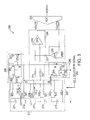
- FIG. 1 shows a conventional cell voltage detection circuit 100.
- the circuit 100 includes a battery pack 110, a cell voltage level shifter 120, and a detection and measurement block 140.
- the battery pack 110 includes battery cells 111-115 as shown in the example of FIG. 1 .
- the level shifter 120 selects a battery cell according to a cell selection signal 180, and shifts the terminal voltages of the selected cell to lower voltages. In such way, the detection and measurement block 140 can measure the cell voltages for the cells 111-115, and output the measured results accordingly.
- the level shifter 120 consumes current from the battery pack 110.
- a current I VH1 flows from the node H1 which is the positive terminal of the cell 112, through the level shifter 120, the cells 115-112, and back to the node H1.
- a current I VL1 flows from the node L1 which is the negative terminal of the cell 112, through the level shifter 120, the cells 115-113, and back to the node L1. Therefore, the capacities of the cells 113-115 are degraded by the currents I VH1 and I VL1 , while the capacity of the cell 112 is degraded by the current I VH1 .
- the level shifter 120 consumes current when measuring cell voltages for other cells, e.g., cells 111 and 113-115.
- the capacities of the cells 119-115 are unbalanced and the cell 115 located at the bottom of the battery 110 may have less capacity compared to other cells 111-114, thus affecting the available capacity of the battery pack 110.
- a circuit used to measure cell voltages in a voltage cell pack includes a cell voltage level shifter, a sense block, and a compensation current generator.
- the cell voltage level shifter selects a cell and shifts the terminal voltages of the selected cell from a first voltage level to a second voltage level.
- the sense block monitors the current consumed by the level shifter, and generates a signal indicative of the consumed current.
- the compensation current generator generates a compensation current to compensate the current consumed by the level shifter. Therefore, unbalance of the cell capacities caused by the current consumed by the level shifter can be reduced or eliminated, and thus the overall capacity of the voltage cell pack can be improved.
- FIG. 1 shows a conventional cell voltage detection circuit for a battery pack.
- FIG. 2 illustrates a block diagram of a circuit for measuring cell voltages of a battery pack, in accordance with one embodiment of the present invention.
- FIG. 3 shows a schematic diagram of a circuit for measuring cell voltages of a battery pack, in accordance with one embodiment of the present invention.
- FIG. 4 shows a schematic diagram of a circuit for measuring cell voltages of a battery pack, in accordance with another embodiment of the present invention.
- FIG. 5 shows a schematic diagram of a circuit for measuring cell voltages of a battery pack, in accordance with another embodiment of the present invention.
- FIG. 6 shows an operational amplifier, in accordance with one embodiment of the present invention.
- FIG. 7 shows an operational amplifier, in accordance with another embodiment of the present invention.
- FIG. 8 shows a flowchart of a method for measuring cell voltages of a battery pack, in accordance with one embodiment of the present invention.
- Embodiments in accordance with the present invention provide detection or measurement circuits for a battery pack.
- a detection circuit can include a level shifter.
- the detection circuit can monitor the current consumed by the level shifter and generate a corresponding compensation current to compensate the current consumed by the level shifter.
- the battery described in the present invention can be, but is not limited to, a Lithium Ion battery or a Lead Acid battery.
- the invention is described in relation to a battery, the invention is not so limited. For example, the invention may also be used in solar cell applications.
- FIG. 2 illustrates a block diagram of a circuit 200 for measuring cell voltages of a battery pack, in accordance with one embodiment of the present invention.
- the circuit 200 includes a battery pack 210, a cell voltage level shifter 220, a detection and measurement block 240, a sense block 250, and a compensation current generator 260.
- the battery pack 210 includes cells 211-215 for illustration purposes but not limitation. The battery pack 210 can include some other number of battery cells.
- the level shifter 220 is coupled to each cell in the battery pack 210 and can select a cell according to a cell selection signal 280 and shift the terminal voltages of the selected cell from a first voltage level to a second voltage level. In one embodiment, the first voltage level is higher than the second voltage level. In one embodiment, one cell is selected at each time.
- the detection and measurement block 240 receives the shifted voltages and measures the cell voltages of the cells 211-215.
- the sense block 250 can monitor a current flowing through a terminal of the selected cell and can generate a sense signal 251 indicative of the current flowing from the terminal of the selected cell to the level shifter 220.
- the sense block 250 can monitor a current IVH2 flowing from the terminal H2 of the cell 212 to the level shifter 220 and/or a current IVL2 flowing from the terminal L2 of the cell 212 to the level shifter 220.
- the sense signal 251 is a sense current.
- the compensation current generator 260 receives the sense signal 251 and generates a compensation current I COMP according to the sense signal 251.
- the compensation current generator 260 can generate the compensation current I COMP by mirroring and/or scaling the signal 251.
- the compensation current I COMP can flow through the battery pack 210 to compensate the current consumed by the level shifter 220. Therefore, the unbalance of the cell capacities caused by the level shifter 220 can be reduced or avoided, and thus the lifetime of the battery pack 210 can be improved.
- FIG. 3 shows a schematic diagram of a circuit 300 for measuring cell voltages of a battery pack, in accordance with one embodiment of the present invention.
- FIG. 3 is described in combination with FIG. 2 .
- the level shifter 220 can include switches 321-330.
- the switches 321-330 can be controlled by a cell selection signal 280.
- the level shifter 220 includes two proportional amplifiers.
- One proportional amplifier includes resistors 332 and 334 and operational amplifier 335, and the other proportional amplifier includes operational amplifier 336.
- the level shifter 220 further includes resistors 331 and 333.
- the switches 321, 322, 324, 326 and 328 are coupled to the positive terminal of the operational amplifier 335 via the resistor 331.
- the switches 323, 325, 327, 329 and 330 are coupled to the negative terminal of the operational amplifier 335 through the resistor 332.
- the resistors 331 and 332 are identical, and the resistors 333 and 334 are identical.
- the level shifter 220 can shift the terminal voltages of a selected cell to voltages V OUTP and V OUTN .
- the shifted voltages V OUTP and V OUTN are the outputs of the amplifier 335 and the amplifier 336, respectively.
- the battery cell 212 is selected and the terminal voltages V H2 and V L2 of the cell 212 are received or sensed by the level shifter 220.
- the level shifter 220 shifts the terminal voltages V H2 and V L2 to the voltages V OUTP and V OUTN respectively.
- the ADC 370 converts the voltage V OUT to a digital signal D OUT .
- the sense block 250 includes a resistor 351 and a current mirror including switches 352 and 353.
- the switches 352 and 353 can be N-channel metal-oxide-semiconductor field effect transistors (NMOSFETs) sinking/sourcing the sense current indicative of the current flowing from the terminal of the selected cell to the level shifter 220.
- NMOSFETs N-channel metal-oxide-semiconductor field effect transistors
- One terminal of the resistor 351 receives one terminal voltage of the selected battery cell, and the other terminal of the resistor 351 receives the gate-source voltage of the switch 352 in the current mirror.
- the width-to-length ratio of the NMOSFET 352 to the width-to-length ratio of the NMOSFET 353 can be 1:1.
- the invention is not so limited; the width-to-length ratio of the NMOSFET 352 to the width-to-length ratio of the NMOSFET 353 can be different from 1:1.
- the sense block 250 can monitor a current flowing through a terminal of the selected cell and can generate a sense signal 251 indicative of the current flowing from the terminal of the selected cell to the level shifter 220.
- the levels of the currents I VH2 and I VL2 consumed by the level shifter 220 are dependent on the reference voltage V REF .
- a current flowing through the sense block 250 e.g., a bias current I B
- I B bias current
- I B bias current flowing through the resistor 351 and the NMOSFET 352
- V GS the gate-source voltage of the NMOSFET 352
- R C the resistance of the resistor 351.
- the term "substantially equal” is used because some difference between the predetermined reference voltage V REF and the gate-source voltage V GS of the NMOSFET 352 is permitted; however, that difference is small enough to be ignored.
- the sense block 250 can sense the current I VH2 and can generate a sensing current I N indicative of the current I VH2 to the compensation current generator 260.
- the sensing current I N can be equal to the current I B .
- I N I VH ⁇ 2 / K .
- the compensation current generator 260 can be a current mirror including P-channel metal-oxide-semiconductor field effect transistors (PMOSFETs) 361, 362 and 363 sinking/sourcing the sense current and the compensation current.
- the width-to-length ratios of the PMOSFETs 361, 362 and 363 can have the proportion 1: (K + 1): K.
- the compensation current generator 260 receives the sensing current I N from the sense block 250, and generates compensation currents I CN3 and ICP3 flowing into the battery pack 210 to compensate the current consumed by the level shifter 220.
- the battery cell 212 is selected.
- the sensing current I N flows through the PMOSFET 361.
- the compensation current I CP3 which is substantially equal to I VH2 + I B , flows through the cells 212-215 in the opposite direction of the currents I VH2 and I B .
- the term "substantially equal” is used because some difference between the compensation current I CP3 and the current I VH2 + I B is permitted; however, that difference is small enough to be ignored.
- the currents I VH2 and I B can be compensated by the compensation current I CP3 . Therefore, the capacity degradation of the cells 212 -215 caused by the current I VH2 can be reduced or eliminated by the compensation current I CP3 .
- the compensation current I CN3 (given by equation (9)) flows through the cells 213-215 in the opposite direction of the current I VL2 .
- the sense block 250 can sense the current consumed by the level shifter 220 and the compensation current generator 260 can generate a compensation current to compensate the current consumed by the level shifter 220.
- the level shifter 220 does not consume current from the negative terminal of the cell 215 (ground), and thus no compensation current flows into the negative terminal of the cell 215 and the current flowing from the PMOSFET 363 can flow into ground. The current flowing from the PMOSFET 362 compensates the consumed current flowing from the positive terminal of the cell 215.
- the sense block 250 and the compensation current generator 260 can still maintain relatively high accuracy even if there are some slight differences between the current consumed by the level shifter 220 and the compensation current generated by the compensation current generator 260.
- FIG. 4 shows a schematic diagram of a circuit 400 for measuring cell voltages of a battery pack, in accordance with another embodiment of the present invention.
- FIG. 4 is described in combination with FIG. 3 .
- the compensation current generator 260 can further include a resistor 466 having the resistance R B and a voltage follower including an operational amplifier 464 and an NMOSFET 465.
- the current I CP3 compensates the current I VH2 + I B in a similar way as in the example in FIG. 3
- a current I CN4 flowing through the switch 325 and the cells 213-215 compensates the current I VL2 .
- I CELL can be a current flowing through the NMOSFET 465 and the resistor 466, in one embodiment.
- the current I VL2 can be compensated by the current I GN4 having the same level as the current I VL2 . Therefore, the capacity degradation of the cells 213-215 caused by the current I VL2 can be reduced or eliminated by the compensation current I CN4 .
- FIG. 5 shows a schematic diagram of a circuit 500 for measuring cell voltages of a battery pack, in accordance with another embodiment of the present invention.
- FIG. 5 is described in combination with FIG. 4 .
- the resistors 331 and 333 and an amplifier 536 included in the level shifter 220 can serve as the sense block 250 to generate a current I O indicative of the current consumed by the level shifter 220.
- the compensation current generator 260 can include PMOSFETs 561, 562 and 563.
- the width-to-length ratios of the PMOSFETs 551, 562 and 563 can meet the proportion 1: K: K. Therefore, both compensation currents I CP5 flowing through the PMOSFET 562 and I CN5 flowing through the PMOSFET 563 are equal to I VH2 .
- the current I CP5 compensates the current I VH2
- the current I CN5 - I CELL compensates the current I VL2
- the circuit in the example of FIG. 5 can compensate the consumed currents without dependence on the gate-source voltage of the NMOSFET 352 in the example of FIG. 4 .
- the circuit in the example of FIG. 5 removes the resistor 351 in the example of FIG. 4 , and thus further reduces the cost of the circuit.
- FIG. 6 shows an embodiment of an operational amplifier 600 which can be used as the operational amplifier 536 shown in FIG. 5 .
- FIG. 6 is described in combination with FIG. 5 .
- the width-to-length ratio of a PMOSFET 606 to the width-to-length ratio of a PMOSFET 609 can be 1: 1.
- the invention is not so limited; the width-to-length ratio of the PMOSFET 606 to the width-to-length ratio of the PMOSFET 609 can be different from 1: 1.
- the width-to-length ratio of a NMOSFET 607 to the width-to-length ratio of a NMOSFET 610 can be K: 1
- the width-to-length ratio of a NMOSFET 608 to the width-to-length ratio of a NMOSFET 611 can also be K: 1.
- the amplifier 600 can be used as the amplifier 536 in FIG. 5 and provide a current I O1 .
- the difference between the current flowing through the resistor 331 and the resistor 333 and the current flowing through the NMOSFETs 607 and 608 can be ignored.
- the current flowing through the NMOSFETs 607 and 608 is approximately equal to I VH2 .
- the current I O1 can be approximately equal to I VH2 /K.
- FIG. 7 shows another embodiment of an operational amplifier 700 which can be used as the operational amplifier 536 shown in FIG. 5 .
- FIG. 7 is described in combination with FIG. 5 and FIG. 6 .
- the PMOSFETs 606 and 609 in FIG. 6 are removed from the amplifier 700 in FIG. 7 . Therefore, the current flowing through the resistors 331 and 333 flows through the NMOSFETs 607 and 608.
- the current I O2 generated by the amplifier 700 can follow the current I VH2 with the proportion 1/K more accurately.
- FIG. 8 illustrates a flowchart of a method 800 for measuring cell voltages of a battery pack.
- FIG. 8 is described in combination with FIG. 2 . Although specific steps are disclosed in FIG. 8 , such steps are examples. That is, the present invention is well suited to performing various other steps or variations of the steps recited in FIG. 8 .
- a cell in a battery pack is selected to detect or measure the cell voltage of the selected cell.
- the level shifter 220 selects a cell in the battery pack 210 according to a cell selection signal.
- the terminal voltages of the selected cell are shifted from a first voltage level to a second voltage level.
- the second voltage level is detected and measured.
- the current consumed during the shifting is monitored, and a sense signal indicative of the consumed current is generated.
- the sense signal is proportional to the current consumed.
- the compensation current flowing through the battery pack 210 to compensate the current consumed is generated according to the sense signal.
- the compensation current is substantially equal to the current consumed.
- the term "substantially equal” is used because some difference between the compensation current and the current consumed is permitted; however, that difference is small enough to be ignored.
- any amount of compensation of the current consumed is beneficial; ideally, the compensation current matches the current consumed.
- the compensation current is generated further according to the second voltage level of the terminal voltage of the selected cell.
- the compensation current can have substantially the same level as the current consumed by the level shifter 220. Therefore, unbalance of the cell capacities caused by the current consumed by the level shifter can be reduced or eliminated, and thus the overall capacity of the battery pack can be improved.
Landscapes
- Physics & Mathematics (AREA)
- General Physics & Mathematics (AREA)
- Measurement Of Current Or Voltage (AREA)
- Secondary Cells (AREA)
- Charge And Discharge Circuits For Batteries Or The Like (AREA)
- Tests Of Electric Status Of Batteries (AREA)
Abstract
A circuit used to measure cell voltages in a battery pack can include a cell voltage level shifter, a sense block, and a compensation current generator. The cell voltage level shifter selects a cell and shifts the terminal voltages of the selected cell from a first voltage level to a second voltage level. The sense block monitors the current consumed by the level shifter, and generates a signal indicative of the consumed current. The compensation current generator generates compensation currents to compensate the current consumed by the level shifter. Therefore, unbalance of the cell capacities caused by the current consumed by the level shifter can be reduced or eliminated, and thus the overall capacity of the battery pack can be improved.
Description
- This application claims priority to
U.S. Provisional Application No. 61/290,563 - Batteries can be used in various applications, such as electric vehicles and hybrid electric vehicles. The workable voltage of a single cell in a battery may be approximately 2~4 volts, but some systems such as the electric vehicles and the hybrid electric vehicles may require higher voltages, e.g., 40 volts. Multiple cells can be coupled to each other in series to drive the electric vehicles and the hybrid electric vehicles.
- In battery management, the status of cells, such as cell voltages, may be detected and measured by a measurement block, e.g., an analog-to-digital converter (ADC). The ADC can be implemented by devices having relatively low voltages. A voltage level shifter can be coupled between the cells and the ADC to shift the terminal voltages of each cell to lower voltages, e.g., from 40 volts to 2 volts, and the ADC detects and measures the cell voltages according to the shifted voltages.
-
FIG. 1 shows a conventional cellvoltage detection circuit 100. Thecircuit 100 includes abattery pack 110, a cellvoltage level shifter 120, and a detection andmeasurement block 140. Thebattery pack 110 includes battery cells 111-115 as shown in the example ofFIG. 1 . Thelevel shifter 120 selects a battery cell according to acell selection signal 180, and shifts the terminal voltages of the selected cell to lower voltages. In such way, the detection andmeasurement block 140 can measure the cell voltages for the cells 111-115, and output the measured results accordingly. - The
level shifter 120 consumes current from thebattery pack 110. By way of example, when thecell 112 is selected, a current IVH1 flows from the node H1 which is the positive terminal of thecell 112, through thelevel shifter 120, the cells 115-112, and back to the node H1. Moreover, a current IVL1 flows from the node L1 which is the negative terminal of thecell 112, through thelevel shifter 120, the cells 115-113, and back to the node L1. Therefore, the capacities of the cells 113-115 are degraded by the currents IVH1 and IVL1, while the capacity of thecell 112 is degraded by the current IVH1. Similarly, thelevel shifter 120 consumes current when measuring cell voltages for other cells, e.g.,cells 111 and 113-115. As a result, the capacities of the cells 119-115 are unbalanced and thecell 115 located at the bottom of thebattery 110 may have less capacity compared to other cells 111-114, thus affecting the available capacity of thebattery pack 110. - In one embodiment, a circuit used to measure cell voltages in a voltage cell pack includes a cell voltage level shifter, a sense block, and a compensation current generator. The cell voltage level shifter selects a cell and shifts the terminal voltages of the selected cell from a first voltage level to a second voltage level. The sense block monitors the current consumed by the level shifter, and generates a signal indicative of the consumed current. The compensation current generator generates a compensation current to compensate the current consumed by the level shifter. Therefore, unbalance of the cell capacities caused by the current consumed by the level shifter can be reduced or eliminated, and thus the overall capacity of the voltage cell pack can be improved.
- The accompanying drawings, which are incorporated in and form a part of this specification and in which like numerals depict like elements, illustrate embodiments of the present invention and, together with the description, serve to explain the principles of the invention:
-
FIG. 1 shows a conventional cell voltage detection circuit for a battery pack. -
FIG. 2 illustrates a block diagram of a circuit for measuring cell voltages of a battery pack, in accordance with one embodiment of the present invention. -
FIG. 3 shows a schematic diagram of a circuit for measuring cell voltages of a battery pack, in accordance with one embodiment of the present invention. -
FIG. 4 shows a schematic diagram of a circuit for measuring cell voltages of a battery pack, in accordance with another embodiment of the present invention. -
FIG. 5 shows a schematic diagram of a circuit for measuring cell voltages of a battery pack, in accordance with another embodiment of the present invention. -
FIG. 6 shows an operational amplifier, in accordance with one embodiment of the present invention. -
FIG. 7 shows an operational amplifier, in accordance with another embodiment of the present invention. -
FIG. 8 shows a flowchart of a method for measuring cell voltages of a battery pack, in accordance with one embodiment of the present invention. - Reference will now be made in detail to the embodiments of the present invention, examples of which are illustrated in the accompanying drawings. While the invention will be described in conjunction with the embodiments, it will be understood that they are not intended to limit the invention to these embodiments. On the contrary, the invention is intended to cover alternatives, modifications and equivalents, which may be included within the spirit and scope of the invention as defined by the appended claims.
- Furthermore, in the following detailed description of embodiments of the present invention, numerous specific details are set forth in order to provide a thorough understanding of the present invention. However, it will be recognized by one of ordinary skill in the art that the present invention may be practiced without these specific details. In other instances, well-known methods, procedures, components, and circuits have not been described in detail as not to unnecessarily obscure aspects of the embodiments of the present invention.
- Embodiments in accordance with the present invention provide detection or measurement circuits for a battery pack. A detection circuit can include a level shifter. Advantageously, the detection circuit can monitor the current consumed by the level shifter and generate a corresponding compensation current to compensate the current consumed by the level shifter. As a result, unbalance of the cell capacities caused by the current consumed by the level shifter can be reduced or eliminated, and thus the overall capacity of the battery pack can be improved. The battery described in the present invention can be, but is not limited to, a Lithium Ion battery or a Lead Acid battery. Although the invention is described in relation to a battery, the invention is not so limited. For example, the invention may also be used in solar cell applications.
-
FIG. 2 illustrates a block diagram of acircuit 200 for measuring cell voltages of a battery pack, in accordance with one embodiment of the present invention. In the example ofFIG. 2 , thecircuit 200 includes abattery pack 210, a cellvoltage level shifter 220, a detection andmeasurement block 240, asense block 250, and a compensationcurrent generator 260. In the example ofFIG. 2 , thebattery pack 210 includes cells 211-215 for illustration purposes but not limitation. Thebattery pack 210 can include some other number of battery cells. - The
level shifter 220 is coupled to each cell in thebattery pack 210 and can select a cell according to acell selection signal 280 and shift the terminal voltages of the selected cell from a first voltage level to a second voltage level. In one embodiment, the first voltage level is higher than the second voltage level. In one embodiment, one cell is selected at each time. The detection andmeasurement block 240 receives the shifted voltages and measures the cell voltages of the cells 211-215. - When the
level shifter 220 selects a cell to shift the terminal voltages of the selected cell, thelevel shifter 220 may consume currents from the terminals of the selected cell. Thesense block 250 can monitor a current flowing through a terminal of the selected cell and can generate asense signal 251 indicative of the current flowing from the terminal of the selected cell to thelevel shifter 220. For example, thesense block 250 can monitor a current IVH2 flowing from the terminal H2 of thecell 212 to thelevel shifter 220 and/or a current IVL2 flowing from the terminal L2 of thecell 212 to thelevel shifter 220. In one embodiment, thesense signal 251 is a sense current. The compensationcurrent generator 260 receives thesense signal 251 and generates a compensation current ICOMP according to thesense signal 251. For example, the compensationcurrent generator 260 can generate the compensation current ICOMP by mirroring and/or scaling thesignal 251. - Advantageously, the compensation current ICOMP can flow through the
battery pack 210 to compensate the current consumed by thelevel shifter 220. Therefore, the unbalance of the cell capacities caused by thelevel shifter 220 can be reduced or avoided, and thus the lifetime of thebattery pack 210 can be improved. -
FIG. 3 shows a schematic diagram of acircuit 300 for measuring cell voltages of a battery pack, in accordance with one embodiment of the present invention.FIG. 3 is described in combination withFIG. 2 . - In the example of
FIG. 3 , thelevel shifter 220 can include switches 321-330. The switches 321-330 can be controlled by acell selection signal 280. In addition, thelevel shifter 220 includes two proportional amplifiers. One proportional amplifier includesresistors operational amplifier 335, and the other proportional amplifier includesoperational amplifier 336. Moreover, thelevel shifter 220 further includesresistors switches operational amplifier 335 via theresistor 331. Theswitches operational amplifier 335 through theresistor 332. In one embodiment, theresistors resistors level shifter 220 can shift the terminal voltages of a selected cell to voltages VOUTP and VOUTN. The shifted voltages VOUTP and VOUTN are the outputs of theamplifier 335 and theamplifier 336, respectively. - By way of example, when the
switches switches 321, 323-324 and 326-330 are off, thebattery cell 212 is selected and the terminal voltages VH2 and VL2 of thecell 212 are received or sensed by thelevel shifter 220. Thelevel shifter 220 shifts the terminal voltages VH2 and VL2 to the voltages VOUTP and VOUTN respectively. The difference VOUT between VOUTP and VOUTN can be given by:
battery cell 212, RB is the resistance of theresistor 333 and the resistance of theresistor 334, RA is the resistance of theresistor 331 and the resistance of theresistor 332, VH2 is the voltage at the node H2 which is the positive terminal of thecell 212, and VL2 is the voltage at the node L2 which is the negative terminal of thecell 212. TheADC 370 converts the voltage VOUT to a digital signal DOUT. - In the example of
FIG. 3 , thesense block 250 includes aresistor 351 and a currentmirror including switches switches level shifter 220. One terminal of theresistor 351 receives one terminal voltage of the selected battery cell, and the other terminal of theresistor 351 receives the gate-source voltage of theswitch 352 in the current mirror. For example, the width-to-length ratio of theNMOSFET 352 to the width-to-length ratio of theNMOSFET 353 can be 1:1. However, the invention is not so limited; the width-to-length ratio of theNMOSFET 352 to the width-to-length ratio of theNMOSFET 353 can be different from 1:1. Thesense block 250 can monitor a current flowing through a terminal of the selected cell and can generate asense signal 251 indicative of the current flowing from the terminal of the selected cell to thelevel shifter 220. - By way of example, when the
switches switches 321, 323-324 and 326-330 are off, thebattery cell 212 is selected. A current IVH2 flowing from the node H2 (positive terminal of the cell 212) through theswitch 322, theresistor 331 andresistor 333 can be given by:
switch 325 and theresistors 
In other words, the levels of the currents IVH2 and IVL2 consumed by thelevel shifter 220 are dependent on the reference voltage VREF. A current flowing through thesense block 250, e.g., a bias current IB, flowing through theresistor 351 and theNMOSFET 352 can be given by:
NMOSFET 352 and RC is the resistance of theresistor 351. RA, RB and RC meet the following equation:

Here the term "substantially equal" is used because some difference between the predetermined reference voltage VREF and the gate-source voltage VGS of theNMOSFET 352 is permitted; however, that difference is small enough to be ignored. Advantageously, thesense block 250 can sense the current IVH2 and can generate a sensing current IN indicative of the current IVH2 to the compensationcurrent generator 260. In one embodiment, the sensing current IN can be equal to the current IB. Thus, the following equation can be obtained:
- In the example of
FIG. 3 , the compensationcurrent generator 260 can be a current mirror including P-channel metal-oxide-semiconductor field effect transistors (PMOSFETs) 361, 362 and 363 sinking/sourcing the sense current and the compensation current. The width-to-length ratios of thePMOSFETs current generator 260 receives the sensing current IN from thesense block 250, and generates compensation currents ICN3 and ICP3 flowing into thebattery pack 210 to compensate the current consumed by thelevel shifter 220. - By way of example, when the
switches switches 321, 323-324 and 326-330 are off, thebattery cell 212 is selected. The sensing current IN flows through thePMOSFET 361. Thus, a current ICP3 flowing through thePMOSFET 362, theswitch 322 and the cells 212-215 can be given by:
PMOSFET 363, theswitch 325 and the cells 213-215 can be given by:
Advantageously, the compensation current ICP3, which is substantially equal to IVH2 + IB, flows through the cells 212-215 in the opposite direction of the currents IVH2 and IB. Here the term "substantially equal" is used because some difference between the compensation current ICP3 and the current IVH2 + IB is permitted; however, that difference is small enough to be ignored. In other words, the currents IVH2 and IB can be compensated by the compensation current ICP3. Therefore, the capacity degradation of the cells 212 -215 caused by the current IVH2 can be reduced or eliminated by the compensation current ICP3. Moreover, the compensation current ICN3 (given by equation (9)) flows through the cells 213-215 in the opposite direction of the current IVL2. In one embodiment, the difference between the compensation current ICN3 and the current IVL2 is small enough to be ignored and can be given by:
Therefore, the capacity degradation of the cells 213-215 caused by the current IVL2 can be reduced by the compensation current ICN3. - Similarly, when the
cell sense block 250 can sense the current consumed by thelevel shifter 220 and the compensationcurrent generator 260 can generate a compensation current to compensate the current consumed by thelevel shifter 220. In one embodiment, when thecell 215 is selected, thelevel shifter 220 does not consume current from the negative terminal of the cell 215 (ground), and thus no compensation current flows into the negative terminal of thecell 215 and the current flowing from thePMOSFET 363 can flow into ground. The current flowing from thePMOSFET 362 compensates the consumed current flowing from the positive terminal of thecell 215. - Furthermore, since the impedance at each cell terminal is relatively low, and the impedances at the outputs of the current mirrors (e.g., nodes A, B, C and D) and the inputs of the level shifter (e.g., nodes C and D) are relatively high, the
sense block 250 and the compensationcurrent generator 260 can still maintain relatively high accuracy even if there are some slight differences between the current consumed by thelevel shifter 220 and the compensation current generated by the compensationcurrent generator 260. -
FIG. 4 shows a schematic diagram of acircuit 400 for measuring cell voltages of a battery pack, in accordance with another embodiment of the present invention.FIG. 4 is described in combination withFIG. 3 . - In the example of
FIG. 4 , besides the current mirror including thePMOSFETs current generator 260 can further include aresistor 466 having the resistance RB and a voltage follower including anoperational amplifier 464 and anNMOSFET 465. In one embodiment, when theswitches switches 321, 323-324 and 326-330 are off, the current ICP3 compensates the current IVH2 + IB in a similar way as in the example inFIG. 3 , while a current ICN4 flowing through theswitch 325 and the cells 213-215 compensates the current IVL2. The current ICN4 can be given by:
NMOSFET 465 and theresistor 466, in one embodiment. By combining the equation (1), the current ICELL can be given by:
Thus, by combining the equations (3), (9), (11) and (12), the following equation can be obtained:
Advantageously, the current IVL2 can be compensated by the current IGN4 having the same level as the current IVL2. Therefore, the capacity degradation of the cells 213-215 caused by the current IVL2 can be reduced or eliminated by the compensation current ICN4. -
FIG. 5 shows a schematic diagram of acircuit 500 for measuring cell voltages of a battery pack, in accordance with another embodiment of the present invention.FIG. 5 is described in combination withFIG. 4 . - In the example of
FIG. 5 , theresistors amplifier 536 included in thelevel shifter 220 can serve as thesense block 250 to generate a current IO indicative of the current consumed by thelevel shifter 220. In one embodiment, the current IO can meet the following equation:
The compensationcurrent generator 260 can includePMOSFETs PMOSFETs PMOSFET 562 and ICN5 flowing through thePMOSFET 563 are equal to IVH2. In such way, the current ICP5 compensates the current IVH2, and the current ICN5 - ICELL compensates the current IVL2. Advantageously, the circuit in the example ofFIG. 5 can compensate the consumed currents without dependence on the gate-source voltage of theNMOSFET 352 in the example ofFIG. 4 . Moreover, the circuit in the example ofFIG. 5 removes theresistor 351 in the example ofFIG. 4 , and thus further reduces the cost of the circuit. -
FIG. 6 shows an embodiment of anoperational amplifier 600 which can be used as theoperational amplifier 536 shown inFIG. 5 .FIG. 6 is described in combination withFIG. 5 . In the example ofFIG. 6 , the width-to-length ratio of aPMOSFET 606 to the width-to-length ratio of a PMOSFET 609 can be 1: 1. However, the invention is not so limited; the width-to-length ratio of thePMOSFET 606 to the width-to-length ratio of thePMOSFET 609 can be different from 1: 1. The width-to-length ratio of aNMOSFET 607 to the width-to-length ratio of a NMOSFET 610 can be K: 1, and the width-to-length ratio of aNMOSFET 608 to the width-to-length ratio of a NMOSFET 611 can also be K: 1. - The
amplifier 600 can be used as theamplifier 536 inFIG. 5 and provide a current IO1. In one embodiment, since the total resistance of theresistor 331 and theresistor 333 in the example ofFIG. 5 is relatively low compared to the on resistance of thePMOSFETs resistor 331 and theresistor 333 and the current flowing through theNMOSFETs NMOSFETs -
FIG. 7 shows another embodiment of anoperational amplifier 700 which can be used as theoperational amplifier 536 shown inFIG. 5 .FIG. 7 is described in combination withFIG. 5 andFIG. 6 . - Compared to the
amplifier 600 inFIG. 6 , thePMOSFETs FIG. 6 are removed from theamplifier 700 inFIG. 7 . Therefore, the current flowing through theresistors NMOSFETs amplifier 700 can follow the current IVH2 with theproportion 1/K more accurately. -
FIG. 8 illustrates a flowchart of amethod 800 for measuring cell voltages of a battery pack.FIG. 8 is described in combination withFIG. 2 . Although specific steps are disclosed inFIG. 8 , such steps are examples. That is, the present invention is well suited to performing various other steps or variations of the steps recited inFIG. 8 . - At
step 812, a cell in a battery pack is selected to detect or measure the cell voltage of the selected cell. For example, thelevel shifter 220 selects a cell in thebattery pack 210 according to a cell selection signal. Atstep 814, the terminal voltages of the selected cell are shifted from a first voltage level to a second voltage level. Atstep 816, the second voltage level is detected and measured. - At
step 818, the current consumed during the shifting is monitored, and a sense signal indicative of the consumed current is generated. In one embodiment, the sense signal is proportional to the current consumed. Atstep 820, the compensation current flowing through thebattery pack 210 to compensate the current consumed is generated according to the sense signal.
In one embodiment, the compensation current is substantially equal to the current consumed. Here the term "substantially equal" is used because some difference between the compensation current and the current consumed is permitted; however, that difference is small enough to be ignored. Generally speaking, any amount of compensation of the current consumed is beneficial; ideally, the compensation current matches the current consumed. In one embodiment, the compensation current is generated further according to the second voltage level of the terminal voltage of the selected cell. Advantageously, the compensation current can have substantially the same level as the current consumed by thelevel shifter 220. Therefore, unbalance of the cell capacities caused by the current consumed by the level shifter can be reduced or eliminated, and thus the overall capacity of the battery pack can be improved. - While the foregoing description and drawings represent embodiments of the present invention, it will be understood that various additions, modifications and substitutions may be made therein without departing from the spirit and scope of the principles of the present invention as defined in the accompanying claims. One skilled in the art will appreciate that the invention may be used with many modifications of form, structure, arrangement, proportions, materials, elements, and components and otherwise, used in the practice of the invention, which are particularly adapted to specific environments and operative requirements without departing from the principles of the present invention. The presently disclosed embodiments are therefore to be considered in all respects as illustrative and not restrictive, the scope of the invention being indicated by the appended claims and their legal equivalents, and not limited to the foregoing description.
Claims (17)
- A circuit, comprising:a level shifter operable for shifting a terminal voltage of a voltage cell, in particular a battery cell or a solar cell, from a first voltage level to a second voltage level;a sense block coupled to said level shifter operable for monitoring the current consumed by said level shifter from said voltage cell and for generating a sense signal indicative of said current;a compensation current generator coupled to said sense block and said level shifter and operable for receiving said sense signal and generating a compensation current flowing into said voltage cell according to said sense signal.
- The circuit of claim 1, wherein said compensation current generator comprises current mirrors operable for sinking/sourcing said compensation current.
- The circuit of claim 1, wherein said compensation current generator further generates said compensation current according to the cell voltage of said voltage cell.
- The circuit of claim 3, wherein said compensation current generator comprises:a voltage follower operable for receiving a voltage signal indicative of one terminal voltage of said voltage cell; anda resistor with one terminal coupled to said voltage follower and the other terminal operable for receiving a voltage indicative of the other terminal voltage of said voltage cell.
- The circuit of claim 1, wherein said level shifter comprises a proportional amplifier.
- The circuit of claim 1, wherein said sense signal is proportional to said current consumed by said level shifter.
- The circuit of claim 1, wherein said sense signal is a sense current, and wherein said sense block comprises an amplifier operable for sinking/sourcing said current consumed by said level shifter and for providing said sense current.
- The circuit of claim 1, wherein said sense signal is a sense current, and wherein said sense block comprises a current mirror operable for sinking/sourcing said current consumed by said level shifter and said sense current.
- The circuit of claim 8, wherein said sense block further comprises a resistor with one terminal receiving said terminal voltage of said voltage cell and the other terminal receiving the gate-source voltage of a switch in said current mirror; wherein said current consumed by said level shifter is dependent on a reference voltage; and wherein said gate-source voltage is substantially equal to said reference voltage.
- The circuit of claim 1, wherein said first voltage level is higher than said second voltage level.
- The circuit of claim 1, wherein said voltage cell is selected according to a cell selection signal.
- The circuit of claim 1, further comprising a detection and measurement block coupled to said level shifter and operable for detecting and measuring said second voltage level.
- Arrangement comprising a plurality of voltage cells, in particular a plurality of battery cells or solar cells, coupled in series, further comprising a circuit according to one of claims 1 - 12, wherein a voltage cell is selected according to a cell selection signal.
- A method for compensating currents within a voltage cell pack, in particular a battery pack or a solar cell pack, said method comprising:selecting a voltage cell in said voltage cell pack to shift;shifting the terminal voltage of said voltage cell from a first voltage level to a second voltage level;monitoring current consumed from said voltage pack as a result of shifting said terminal voltage from said first voltage level to said second voltage level;generating a sense signal indicative of said current consumed because of said shifting; andgenerating a compensation current according to said sense signal, said compensation current flowing into said voltage cell pack.
- The method of claim 14, wherein said method further comprises:detecting said second voltage level.
- The method of claim 14, wherein said sense signal is a sense current, and wherein said generating said compensation current comprises mirroring said sense current .
- The method of claim 14, further comprising:generating said compensation current according to the cell voltage of said voltage cell.
Applications Claiming Priority (2)
| Application Number | Priority Date | Filing Date | Title |
|---|---|---|---|
| US29056309P | 2009-12-29 | 2009-12-29 | |
| US12/955,604 US8629679B2 (en) | 2009-12-29 | 2010-11-29 | Circuits and methods for measuring cell voltages in battery packs |
Publications (1)
| Publication Number | Publication Date |
|---|---|
| EP2343565A2 true EP2343565A2 (en) | 2011-07-13 |
Family
ID=43779599
Family Applications (1)
| Application Number | Title | Priority Date | Filing Date |
|---|---|---|---|
| EP10196825A Withdrawn EP2343565A2 (en) | 2009-12-29 | 2010-12-23 | Circuits and methods for measuring cell voltages in battery packs |
Country Status (5)
| Country | Link |
|---|---|
| US (1) | US8629679B2 (en) |
| EP (1) | EP2343565A2 (en) |
| JP (1) | JP2011137813A (en) |
| CN (1) | CN102121972B (en) |
| TW (1) | TWI418114B (en) |
Families Citing this family (25)
| Publication number | Priority date | Publication date | Assignee | Title |
|---|---|---|---|---|
| US20130041606A1 (en) * | 2011-08-10 | 2013-02-14 | XiaoHu Tang | Detecting an open wire between a battery cell and an external circuit |
| US9190859B1 (en) * | 2010-06-04 | 2015-11-17 | Marvell International Ltd. | Voltage reference buffer using voltage battery level shifter |
| DE102010034510A1 (en) * | 2010-08-16 | 2012-02-16 | Atmel Automotive Gmbh | Circuit for monitoring accumulator cells connected in series |
| US9098309B2 (en) | 2011-09-23 | 2015-08-04 | Qualcomm Incorporated | Power consumption optimized translation of object code partitioned for hardware component based on identified operations |
| US20130162214A1 (en) * | 2011-12-21 | 2013-06-27 | Metal Industries Research & Development Centre | Capacitor active balancing device with high-voltage differential and method thereof |
| US8922218B2 (en) * | 2011-12-28 | 2014-12-30 | O2Micro Inc | Detection circuits for batteries |
| US20130185581A1 (en) * | 2012-01-18 | 2013-07-18 | Qualcomm Incorporated | Efficient Code Dispatch Based on Performance and Energy Consumption |
| CN102590592A (en) * | 2012-03-05 | 2012-07-18 | 绍兴光大芯业微电子有限公司 | Device for precisely detecting voltage of lithium battery pack |
| TWI451112B (en) * | 2012-06-21 | 2014-09-01 | Via Tech Inc | Battery management system |
| CN102759652A (en) * | 2012-06-28 | 2012-10-31 | 河南省电力公司信阳供电公司 | Solar high-voltage presence indicating device |
| TWI533007B (en) * | 2012-08-15 | 2016-05-11 | 凹凸科技國際股份有限公司 | Circuits and methods for measuring a cell voltage in a battery |
| JP6741945B2 (en) * | 2016-09-13 | 2020-08-19 | ミツミ電機株式会社 | Battery control circuit |
| CN106771493A (en) * | 2016-12-27 | 2017-05-31 | 安徽力高新能源技术有限公司 | A kind of multi-series lithium battery voltage detecting circuit based on mirror current source |
| CN106645915A (en) * | 2016-12-27 | 2017-05-10 | 安徽力高新能源技术有限公司 | Image current source multiple series battery voltage detection circuit-based temperature drift compensation circuit |
| US11223074B2 (en) | 2017-10-16 | 2022-01-11 | Neapco Intellectual Property Holdings, Llc | Battery cell monitoring system |
| US11264653B2 (en) | 2017-10-16 | 2022-03-01 | Neapco Intellectual Property Holdings, Llc | Battery cell monitoring system |
| US10412805B1 (en) * | 2018-05-16 | 2019-09-10 | Black & Decker Inc. | Control method and apparatus for extending runtime on a portable lighting device |
| CN110611295B (en) * | 2019-09-04 | 2022-03-25 | 成都芯港微电子有限公司 | Current compensation circuit of lithium battery protection chip |
| CN111769616B (en) * | 2020-07-09 | 2021-06-25 | 珠海迈巨微电子有限责任公司 | Battery voltage monitoring device and battery management system |
| CN114384437B (en) * | 2020-10-16 | 2025-07-18 | 凹凸电子(武汉)有限公司 | Controller and battery voltage detection method |
| KR20220118138A (en) * | 2021-02-18 | 2022-08-25 | 주식회사 엘지에너지솔루션 | Battery protection circuit implementing secondary protection IC function, voltage measurement method and battery protection method of series-connected cells using the same |
| CN113224819B (en) * | 2021-05-25 | 2022-06-21 | 中国人民解放军国防科技大学 | Voltage conversion circuit and battery protection chip |
| CN114336853B (en) * | 2021-12-29 | 2023-11-28 | 西安华泰半导体科技有限公司 | Equalization circuit structure for multiplexing sampling circuit during multi-lithium battery component |
| US20240175924A1 (en) * | 2022-11-30 | 2024-05-30 | O2Micro Inc. | Battery monitoring circuits |
| EP4645635A1 (en) * | 2024-04-29 | 2025-11-05 | NXP USA, Inc. | A driver circuit and method for a battery management system |
Family Cites Families (12)
| Publication number | Priority date | Publication date | Assignee | Title |
|---|---|---|---|---|
| US7058525B2 (en) * | 1999-04-08 | 2006-06-06 | Midtronics, Inc. | Battery test module |
| JP3620517B2 (en) * | 2002-06-12 | 2005-02-16 | 日産自動車株式会社 | Voltage control device for battery pack |
| US7081737B2 (en) * | 2003-06-19 | 2006-07-25 | O2Micro International Limited | Battery cell monitoring and balancing circuit |
| JP4340514B2 (en) | 2003-10-28 | 2009-10-07 | パナソニック株式会社 | Battery voltage measuring device and battery pack |
| US7417405B2 (en) | 2004-10-04 | 2008-08-26 | Black & Decker Inc. | Battery monitoring arrangement having an integrated circuit with logic controller in a battery pack |
| CN100463435C (en) | 2005-02-04 | 2009-02-18 | 美国凹凸微系有限公司 | Uncommon serial bus physical layer implementation |
| US8278876B2 (en) | 2005-03-07 | 2012-10-02 | O2Micro, Inc. | Battery pack current monitoring |
| US7352155B2 (en) * | 2006-06-12 | 2008-04-01 | O2Micro International Ltd. | Apparatus and method for detecting battery pack voltage |
| CN100589305C (en) | 2006-09-29 | 2010-02-10 | 美国凹凸微系有限公司 | Trickle discharge method for battery pack protection |
| US7466104B2 (en) * | 2006-10-13 | 2008-12-16 | O2 Micro International Limited | System and method for balancing cells in a battery pack with selective bypass paths |
| US7965061B2 (en) | 2008-02-01 | 2011-06-21 | O2Micro, Inc. | Conversion systems with balanced cell currents |
| US8502503B2 (en) * | 2008-12-18 | 2013-08-06 | O2Micro Inc. | Circuits and methods for protection of battery modules |
-
2010
- 2010-11-29 US US12/955,604 patent/US8629679B2/en active Active
- 2010-12-17 JP JP2010281924A patent/JP2011137813A/en active Pending
- 2010-12-20 CN CN201010610043.3A patent/CN102121972B/en active Active
- 2010-12-23 EP EP10196825A patent/EP2343565A2/en not_active Withdrawn
- 2010-12-28 TW TW099146269A patent/TWI418114B/en active
Non-Patent Citations (1)
| Title |
|---|
| None |
Also Published As
| Publication number | Publication date |
|---|---|
| US20110074431A1 (en) | 2011-03-31 |
| US8629679B2 (en) | 2014-01-14 |
| TWI418114B (en) | 2013-12-01 |
| CN102121972A (en) | 2011-07-13 |
| TW201131936A (en) | 2011-09-16 |
| CN102121972B (en) | 2014-03-12 |
| JP2011137813A (en) | 2011-07-14 |
Similar Documents
| Publication | Publication Date | Title |
|---|---|---|
| EP2343565A2 (en) | Circuits and methods for measuring cell voltages in battery packs | |
| US8305035B2 (en) | Energy storage device | |
| CN101093245B (en) | Device and method for detecting voltage of battery pack | |
| CA2069858C (en) | Circuit for measuring battery current | |
| EP1391962A1 (en) | Voltage measuring circuit of battery pack | |
| JP4858378B2 (en) | Cell voltage monitoring device for multi-cell series batteries | |
| US7567116B2 (en) | Voltage converting circuit and battery device | |
| US8416012B2 (en) | Reference voltage generating circuit and analog circuit using the same | |
| US20080079434A1 (en) | Car power source apparatus | |
| US8120209B2 (en) | Voltage sensing device for an individual cell of a group of battery cells | |
| US20130002261A1 (en) | Battery pack | |
| JP6767769B2 (en) | Semiconductor devices, battery monitoring systems, and detection methods | |
| KR20080022486A (en) | Battery total voltage detection and leak detection device | |
| KR20080001637A (en) | Current detection circuit | |
| US20130162052A1 (en) | Protective circuit for a rechargeable battery pack | |
| US8922218B2 (en) | Detection circuits for batteries | |
| CN103901260A (en) | Voltage detecting device for assembled battery | |
| JP4719972B2 (en) | Charge / discharge current measuring device | |
| EP3336565B1 (en) | Secondary battery monitoring device and method for diagnosing failure | |
| JP2018013414A (en) | Battery monitoring system | |
| US20140111215A1 (en) | Analogue measurement data detection system and battery voltage detection system | |
| JP2010122162A (en) | Power supply device | |
| JP2007149561A (en) | Circuit and method for detecting electric leakage in battery pack | |
| US6646442B2 (en) | Voltage detection device for a battery package | |
| JP5561049B2 (en) | Battery voltage measuring device |
Legal Events
| Date | Code | Title | Description |
|---|---|---|---|
| PUAI | Public reference made under article 153(3) epc to a published international application that has entered the european phase |
Free format text: ORIGINAL CODE: 0009012 |
|
| AK | Designated contracting states |
Kind code of ref document: A2 Designated state(s): AL AT BE BG CH CY CZ DE DK EE ES FI FR GB GR HR HU IE IS IT LI LT LU LV MC MK MT NL NO PL PT RO RS SE SI SK SM TR |
|
| AX | Request for extension of the european patent |
Extension state: BA ME |
|
| STAA | Information on the status of an ep patent application or granted ep patent |
Free format text: STATUS: THE APPLICATION IS DEEMED TO BE WITHDRAWN |
|
| 18D | Application deemed to be withdrawn |
Effective date: 20160701 |